 Open Access Article
Creative Commons Attribution 3.0 Unported Licence
Controlling the charge state of supported nanoparticles in catalysis: lessons from model systems
Gianfranco
Pacchioni
 a and
Hans-Joachim
Freund
*b
aDipartimento di Scienza dei Materiali, Università di Milano-Bicocca, Via R. Cozzi, 55, 20125, Milano, Italy
bFritz-Haber-Institut der Max-Planck-Gesellschaft, Department of Chemical Physics, Faradayweg 4-6, 14195 Berlin, Germany. E-mail: freund@fhi-berlin.mpg.de
First published on 26th April 2018
Abstract
Model systems are very important to identify the working principles of real catalysts, and to develop concepts that can be used in the design of new catalytic materials. In this review we report examples of the use of model systems to better understand and control the occurrence of charge transfer at the interface between supported metal nanoparticles and oxide surfaces. In the first part of this article we concentrate on the nature of the support, and on the basic difference in metal/oxide bonding going from a wide-gap non-reducible oxide material to reducible oxide semiconductors. The roles of oxide nanostructuring, bulk and surface defectiveness, and doping with hetero-atoms are also addressed, as they are all aspects that severely affect the metal/oxide interaction. Particular attention is given to the experimental measures of the occurrence of charge transfer at the metal/oxide interface. In this respect, systems based on oxide ultrathin films are particularly important as they allow the use of scanning probe spectroscopies which, often in combination with other measurements and with first principles theoretical simulations, allow full characterization of small supported nanoparticles and their charge state. In a few selected cases, a precise count of the electrons transferred between the oxide and the supported nanoparticle has been possible. Charge transfer can occur through thin, two-dimensional oxide layers also thanks to their structural flexibility. The flow of charge through the oxide film and the formation of charged adsorbates are accompanied in fact by a substantial polaronic relaxation of the film surface which can be rationalized based on electrostatic arguments. In the final part of this review the relationships between model systems and real catalysts are addressed by discussing some examples of how lessons learned from model systems have helped in rationalizing the behavior of real catalysts under working conditions.
1 Introduction
Heterogeneous catalysts, used in industrial as well as in environmental catalysis, often consist of metal nanoparticles 2–10 nm in size, stabilized on an inorganic support.1–5 The use of metal nanoparticles is thus intrinsic to catalysis, and for this reason, has been classified as one of the first examples of nanotechnology.6 Metal catalysts are usually prepared by wet impregnation on an oxide support, either a porous material, or a polycrystalline oxide. For a long time, it has been assumed that the oxide acts mainly as an “inert” support to disperse and stabilize the metal nanoparticles; according to this view, the metal is the only active species in the catalytic process. The conceptual approach has changed over the years, in particular in connection with catalysts based on very tiny metal nanoparticles, small clusters containing up to 10 atoms, and even single metal atoms.7 New sophisticated techniques have been developed to grow metal particles of dimensions of the order of 1 nm and below, a regime where quantum size effects8 become dominant. Some of these materials, such as clusters of Ag and Pt, containing 3 to 10 atoms, stabilized on porous alumina have shown surprising results in terms of activity and selectivity.9,10 More accurate characterization methods also became available, and they allowed better identification of the nature, structure and composition of a nano-catalyst, in particular under operating conditions. Transmission electron microscopy (TEM) with aberration correction11 and in operando or in situ spectroscopy are prominent examples of those novel techniques.12 High-resolution TEM made it possible to identify the presence of very small metal aggregates, sometimes containing just a few metal atoms on the surfaces of powder catalysts,13 and operando spectroscopy allows for spectroscopic characterization of the catalyst during the measurement of the catalytic activity and selectivity, thus providing a closer look at structure/reactivity relationships.14Many studies have progressively shown that an oxide support cannot always be considered as a simple “spectator”. In fact, its intimate interaction with the supported particles may result in considerable changes in the physical properties and chemical activity of the catalyst. This is particularly relevant when the particle size decreases below 1 nm. Here, the strength and nature of the interaction between the metal aggregate and the oxide support become crucial.
In some cases the chemical bonds at the metal/oxide interface are weak, and dominated by dispersion forces and polarization effects. In the majority of cases, though, new chemical bonds form due to the mixing of metal and oxide orbitals.15 This may be accompanied by net electron transfer, with oxidation or reduction of the metal unit depending on a number of external conditions, primarily the nature of the oxide support.16,17 The complexity of the interaction of the metal catalyst with the support reflects the complexity of an oxide surface: for instance, the same metal can behave very differently, depending on whether the interaction involves mainly the surface anions, the cations, or both.
The extreme case is that of an isolated metal atom. Take a common oxide such as TiO2 and a gold atom (gold on titania has attracted enormous interest because of the Haruta and Hutchings discovery of the catalytic properties of nanostructured gold).18,19 A Au atom binds weakly to the Ti4+ ions of the TiO2(110) rutile surface via polarization forces,20 binds with a moderate Au–O chemical bond with the surface oxide anions, and gives rise to net charge transfer from the surface towards Au, which becomes negatively charged, if the interaction involves a defect center such as an oxygen vacancy.20 Thus, a completely different behavior arises from the interaction of a metal atom (or a small cluster as well) and the various sites available on a support surface.
Of course, also the nature of the metal plays an important role. For the same stoichiometric TiO2(110) surface, while Au remains neutral and forms a covalent bond with the O anions of the surface, adsorbed Cu and Ag atoms reduce the oxide by direct electron transfer and form supported Cu+ and Ag+ cations,21 thus binding to the surface via a completely different mechanism from that of gold.
These simple examples may illustrate the complexity of the interaction of small metal clusters with oxide surfaces. However, additional factors contributing to the overall scenario need to be considered. For instance, reducing the dimensions of the oxide support, i.e. generating oxide nanostructures as nanoparticles, nanowires, or thin films, may result in completely different properties of the oxide, and, hence, modify the interaction with a metal. The catalytic properties of the oxide support can also be modified via selective doping:22 the presence of extrinsic defects may completely change the nature of the support, from electron-rich to electron-deficient, and can also be used to tune the properties of the supported particle. Specific examples in this direction will be illustrated in this review.
Thus, the perturbation in the electronic structure of a metal nanoparticle due to the interaction and, in particular, electron exchange with the oxide support plays a crucial role in the chemistry of the system and in the catalytic activity. To describe this kind of interaction, the term electronic metal support interaction (EMSI) was coined by Campbell.23 This should not be confused with the classical notion of strong metal support interaction (SMSI),24,25 an effect observed under operating conditions and consisting of the formation of an oxide layer covering the surface of the supported metal particles. SMSI and related phenomena of encapsulation often lead to a reduction, if not to the complete suppression, of the catalytic activity typically observed for the pure metal. EMSI, on the other hand, refers to the interaction of the supported metal particle with the oxide support, an effect that may lead to a change in catalytic activity, and sometimes to an enhanced catalytic activity,26 as the charge transfer at the interface can be used in principle to tune the electronic and chemical properties of the metal particle.
Various authors, Schwab, Solymosy, Vol’kenstein,27–29 and others, have addressed the problem of the influence of the support on the catalyst's properties. The “Electronic Theory of Catalysis” is the conceptual framework that tries to rationalize and classify these effects.
The study of the interactions between a metal nanoparticle and an oxide support, and the control of the occurrence and direction of charge transfer have thus become central in the elucidation and rationalization of the catalytic properties of metal/oxide catalysts. Due to the efforts in the development of new preparation and characterization techniques,30–32 often combined with accurate theoretical methods,33 it became possible to create the premise for a deeper understanding of the problem.
The identification of charge transfer at a metal/oxide interface is not always straightforward, and may require a detailed theoretical analysis. Experimentally, a standard method applied to quantify charge transfer at metal nano-particle/oxide interfaces is X-ray photoemission spectroscopy (XPS). The proper interpretation of the spectra in terms of charge transfer is rather complex and requires distinguishing between the initial and final state effects, which depend on the particle size.34 In particular, shifts towards high binding energies are often observed for small supported nano-particles as compared to the bulk, but are not necessarily connected to the existence of a positive charge.35,36 Another method is electron paramagnetic resonance (EPR), which changes as the spin state of a system varies and may be used when applied to model systems or powder samples. In certain cases, where the structure of a nanoparticle is known from scanning tunneling microscopy (STM) and the various states and symmetries of the system, if present, have been determined by scanning tunneling spectroscopy (STS) (i.e. conductance imaging), it may become possible to count the number of electrons that have been transferred. There are a few case studies reported in the literature,37–39 some of which have already been reviewed.40 Nevertheless, some examples are included in Section 3.2 in order to illustrate the method.
As an alternative, the nature of a metal–oxide system may be studied by investigating the support instead of the metal particle. Let's take for instance the case of Ag and Pt metal particles deposited on cerium oxide, CeO2.41 Indirect proof that the Ag and Pt clusters are oxidized when deposited on CeO2(111) surfaces comes from the fact that the typical Ce 4f-XPS signal contains components characteristic of Ce3+, indicating that some Ce ions are reduced from Ce4+ to Ce3+. This approach has recently been used to quantify the charge transfer.42
Another route contributing to the reduction of an oxide surface is the so-called oxygen spillover, i.e. the diffusion of O atoms from the oxide surface to the metal nanoparticle. In the case of ceria the reaction reads as:43
| Mn (M = Ag or Pt) + CeO2(111) → MnOx + CeO2−x(111) | (1) |
Having underlined the complexity inherent to the measurement of charge transfer at metal/oxide interfaces, we move now to analyze more in detail these phenomena. We start by describing the nature of the oxide support.
2 Nature of the support: oxide surfaces, nanostructuring and doping
2.1 Defect-free oxide surfaces
Inorganic oxides exhibit a wide range of properties and behaviors.45,46 Some oxides, such as SiO2, Al2O3, and ZrO2, are wide gap insulators; others such as WO3 and TiO2 exhibit semiconducting behavior; some oxides belong to the special class of magnetic insulators, such as NiO and CuO, and are described by the Hubbard model and characterized by conductivity via hopping. There are also oxides with classical metallic behavior, and ReO3 and tungsten bronzes (NaxWO3) are classical examples. Depending on the level of defectiveness, and on external parameters such as temperature and pressure, some oxides can undergo a non-metal to metal transition, and convert from one class to the other. Finally, there are oxides that, below a critical temperature, become superconducting.From a chemical perspective, oxides and their surfaces47 can be roughly classified into non-reducible oxides, where the metal cation does not easily change the oxidation state, and reducible oxides, where the metal cation can assume different oxidation states and exhibit rich redox chemistry. We will see that this distinction is quite relevant to understand the bonding mechanism with supported metals. To the first category belong simple binary oxides such as Al2O3, SiO2, ZrO2, MgO and many others; the second group is that of transition metal and rare-earth oxides (from TiO2 to CeO2, NiO, WO3, etc.). The binding properties of these two groups of materials are completely different, in particular when one considers charge transfer phenomena at the metal/oxide interface. In this section we will discuss mainly SiO2, MgO, and ZrO2 as typical examples of non-reducible oxides, and TiO2 and CeO2 as representative examples of reducible oxides. The general concepts illustrated can be easily transferred to any kind of oxide.
These oxides are also defined as non-reducible. A quantitative measure of this property is provided by the energy cost to chemically reduce the oxide, for instance by removing oxygen from the structure. However, as we will show below, these concepts are generally valid only if one is considering a bulk oxide. Things can change radically when the oxide is nanostructured. Nanostructuring consists of producing an oxide in the form of nano-particles, nano-rods, or nano-films. The number of low-coordinated oxygen anions and metal cations changes, and increases with respect to the total of fully coordinated bulk ions. Ions at exposed sites like steps, edges, and corners48,49 have the corresponding energies of their O 2p levels destabilized, because of a local reduction of the Madelung potential. The O 2p levels thus move up in energy, and may give rise to new states in the electronic gap of the material. The same occurs, but in the opposite direction, with the empty cation ns and np states that move down in energy with respect to the bottom of the conduction band when the coordination is decreased.50 This has the effect to reduce the band gap of the oxide nanostructure, and to increase the tendency to donate (O sites) or accept (cation sites) electrons from the metal deposits. We will show in the following the consequences of nanostructuring by discussing the properties of the ZrO2 bulk and nanoparticles in H2 adsorption.
To illustrate not only some of these concepts but also the subtle problems connected with a direct measurement of charge transfer between a metal and the oxide support, we use the example of a single K atom adsorbed on alkaline-earth oxides. K is a highly reducing species, and is an ideal candidate to check (a) if electrons can be transferred to the oxide from the adsorbate and (b) the measurable consequences of this electron transfer.51 The nature of the bonding of K with the surface of polycrystalline MgO has been studied in detail by combining EPR (Fig. 1a) with first principles DFT calculations. The experiments have shown that (a) K atoms are bound to at least three surface oxygen anions of the MgO surface (by analyzing the hyperfine coupling constants), (b) the K atoms are thermally stable up to ≈400 K (corresponding to a surface binding energy of ≈1 eV), and (c) the spin distribution of the K atom is strongly perturbed by the interaction with the substrate.51 What the experiments cannot directly indicate is the preferred adsorption site, the reason for the high thermal stability, and, most important, the occurrence of charge transfer to or from the surface. These questions can be addressed using DFT calculations51 which show that K atoms bind very weakly to the regular five-coordinated oxide anions (O5c) of MgO terrace sites (about 0.2 eV, an energy incompatible with the observed high thermal stability). In fact, once deposited on the MgO surface, the K atoms diffuse rapidly until they become stabilized at particular sites called reverse corners, formed by the intersection of two monoatomic steps, Fig. 1b. Here the K atom is strongly bound (by about 1 eV) and interacts with two O4c ions and an O5c ion of the surface. The interaction with three oxygen atoms of the surface is what has been deduced from experiments.
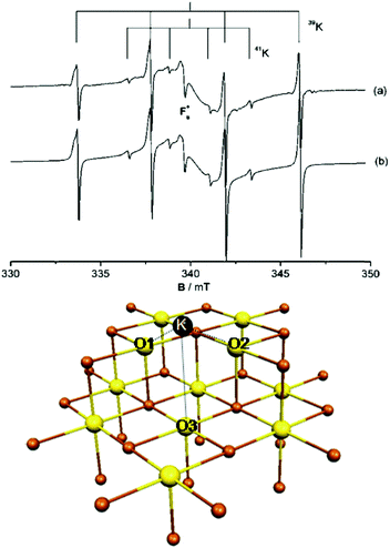 | ||
| Fig. 1 Top: Experimental (a) and simulated (b) EPR spectra of K atoms deposited on MgO (spectra recorded at 77 K). Bottom: K atom adsorbed on the anionic reverse corner of the MgO surface. O atoms yellow, Mg atoms brown; O1 and O2 are O4c ions, and O3 is an O5c ion.51 Reproduced with permission from ref. 51. Copyright American Chemical Society, 2005. | ||
The stabilization of K atoms in the reverse corner sites of MgO leads to a strong polarization of the K 4s orbital. In fact, the interaction with the surface destabilizes the K 4s level. This deformation of the spin distribution results also in isotropic hyperfine coupling constants (aiso) much smaller than on the free atom. Since aiso directly measures the spin density at the nucleus, a simple interpretation could be that the reduction of aiso reflects a partial depopulation of the K 4s orbital due to charge transfer to the oxide support. This view is incorrect. DFT calculations reproduce quantitatively the observed hyperfine interaction, but show unambiguously that a full electron resides in the valence band of the K atom. The interaction with the surface leads to a strong mixing of the spherical 4s orbital and the directional 4p orbitals, resulting in a strong reduction of the isotropic component. Thus, no charge transfer occurs, and the strong change in aiso(K) has a different origin. This is an example of the added value of combining EPR measurements with DFT calculations.
The situation is similar for Li atoms adsorbed on MgO.52 Here, due to different experimental conditions, the Li atoms are adsorbed at low temperature and bind directly to the O5c ions of the surface. The isotropic hyperfine coupling constant of a Li atom adsorbed on top of O5c on the (100) terrace of MgO is aiso = 74 G. This value is about 50% smaller than the aiso value for a free Li atom (143 G in the experiment, 155 G in the calculations). Also in this case it is tempting to conclude that half an electron has been removed from the Li 2s orbital and “donated” to the surface. However, the spin density on the adsorbed Li atom is close to 1 and the large reduction in aiso is due to the polarization of the Li valence electron, as for the K case described above.51–53
The calculations show that if a Li atom is adsorbed on reverse corner sites, where the interaction is stronger, then the aiso value is further reduced to 16 G, about 1/10 of the free atom value (calculated values).53 Once more, this could be misinterpreted, and attributed to a full ionization of the Li atom. Spin density maps obtained from DFT calculations clearly show that the electron is almost entirely localized on Li, but strongly polarized, with consequent reduction of the isotropic constant. The Li atom is virtually neutral, and no charge transfer occurs.53
The general message is that there is little electron transfer at the boundary between alkali metal atoms and the surface of a simple non-reducible oxide like MgO, as expected, but that a direct measurement of this from EPR is not trivial.
Of course, the picture can change dramatically in the presence of defects. If defects or dopants introduce acceptor levels in the band gap, these may lead to a spontaneous ionization of the adsorbed atoms or metal clusters, with the formation of positively charged species. Control over the concentration and nature of defects at the surface of an oxide is thus very important to determine the characteristics of the metal/oxide interface bonding and will be discussed in Section 2.2.
On the regular (101) ZrO2 surface, the H2 molecule dissociates through a classical heterolytic mechanism, in which Zr–H− and O–H+ bonds are formed. This process is slightly exothermic (−0.06 eV, Fig. 2a). The splitting through a homolytic mechanism (formation of two O–H+ bonds and reduction of two Zr4+ centers to Zr3+) is highly endothermic (1.69 eV, Fig. 2d). So, in the absence of defects, heterolytic splitting of H2 is the only viable mechanism on the extended (101) surface, consistent with the non-reducible nature of the oxide.
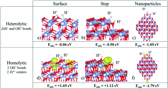 | ||
| Fig. 2 Structures of hydrogen adsorbed on (a and d) the ZrO2(101) surface, (b and e) the ZrO2(156) stepped surface, and (c and f) a Zr80O160 nanoparticle. Top: Heterolytic dissociation; bottom: homolytic dissociation. Zr atoms are represented by big blue spheres, O atoms by small red spheres and H atoms by small grey spheres. In the homolytic mechanism, the spin density localized in reduced Zr3+ centers is represented in yellow (ρiso = 0.01 e− Å−3). Reproduced with permission from ref. 54. Copyright American Chemical Society, 2016. | ||
Of course, a real surface can also contain morphological defects, and in particular linear steps. Ions at steps behave differently from ions at terraces, and the ZrO2(156) stepped surface has been considered. Also in this case the splitting results in H− and H+ ions (heterolytic splitting). Not surprisingly, the reaction is more favorable than on the regular surface, and is exothermic by −0.50 eV, Fig. 2b (the reaction energy was −0.06 eV on the regular terrace). The homolytic splitting (two H+ ions and two Zr3+ centers) remains endothermic, by 1.12 eV, Fig. 2e, but the energy cost is considerably smaller than on the regular surface (1.69 eV). The heterolytic mechanism remains preferred also on step sites of zirconia. Stated differently, zirconia is not reduced upon simple exposure to hydrogen, as this process results in the formation of hydride ions and not in the reduction of Zr4+ to Zr3+.
Now let us consider nanostructured zirconia, in particular in the form of stoichiometric zirconia nanoparticles of size up to 2 nm and zirconia ultrathin films deposited on Pt and Pt3Zr alloys.
When H2 is adsorbed on zirconia nanoparticles, a different picture is observed with respect to the regular surface. On a Zr80O160 nanoparticle, both H2 dissociative mechanisms, heterolytic and homolytic, become exothermic, indicating a much higher reactivity of the nanoparticle compared to that of the bulk material, Fig. 2c and f. More surprising is the fact that the homolytic (reductive) dissociation process becomes the preferred mechanism (the H2 dissociative adsorption energy is −1.79 eV for homolytic vs. −1.05 eV for heterolytic dissociation, Fig. 2c and f). This is opposite to that found for the regular terrace or the stepped surfaces. A similar behavior has been found also for smaller ZrO2 nanoparticles.54
The opposite behavior in H2 dissociation in ZrO2 nanoparticles and extended surfaces is a consequence of nanostructuring, and in particular of the special electronic structure displayed by the nanoparticles.55 This is clearly shown by a comparison of the density of states (DOS) curves for bulk, surface, stepped and nanostructured zirconia, Fig. 3. The presence of under-coordinated sites in the nanoparticles introduces low-lying acceptor states in the band gap that promote the formation of reduced Zr3+ centers through net charge transfer from H2. Nanostructuring makes zirconia a reducible oxide, at variance with the bulk solid.
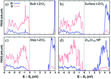 | ||
| Fig. 3 Projected densities of states of (a) bulk tetragonal zirconia, t-ZrO2, (b) a regular (101) t-ZrO2 surface, (c) a stepped (156) t-ZrO2 surface, and (d) a Zr80O160 nanoparticle. The zero energy corresponds to the Fermi level. Red dotted line: O contributions; blue solid line: Zr contributions. Reproduced with permission from ref. 55. Copyright American Chemical Society, 2016. | ||
The other example of oxide nanostructures considered consists of ZrO2 ultra-thin films. A two-dimensional (2D) phase of zirconia does not exist in nature. However, ZrO2/Pt3Zr and ZrO2/Pt 2D films have been prepared and characterized experimentally.56–62 According to DFT calculations, a free-standing, fully relaxed ZrO2 2D film is even less reactive towards hydrogen than the (101) surface.63 In fact, H2 adsorption on the relaxed 2D film is a highly endothermic process: H2 dissociates heterolytically with an energy cost of +1.55 eV, and homolytically with an energy cost of +3.40 eV. This is the consequence of the lattice contraction. In fact, if H2 is adsorbed on a 8.2% strained ZrO2 thin film (the film is computed at the bulk lattice parameter, and subjected to considerable tensile strain), exothermic adsorption energies of −1.38 and −0.11 eV, respectively, are found for the heterolytic and homolytic dissociation mechanisms. Thus, strain in nanostructured oxide films can play a very important role in their reactivity. On unsupported ZrO2 mono-layer films, the heterolytic dissociation remains preferred, as for the regular surface. Thus, zirconia becomes a reducible oxide when produced in a 1D form (nanoparticles), see above, while free-standing 2D nanostructures maintain the low reducible character typical of the bulk.63 The reason is that the coordination of the Zr ions in the 2D film remains the same as that on the (101) surface, while a high-number of low-coordinated Zr ions are present on the nanoparticles.
A completely different picture emerges when a ZrO2 2D film is supported on Pt3Zr or on Pt metals.63 Here the films are moderately strained with respect to the bulk lattice parameter (1 to 4%). In all cases the homolytic dissociation becomes preferred. On ZrO2/Pt3Zr(0001), H2 dissociates homolytically with an energy gain of −1.80 eV, and heterolytically with an energy cost of +0.88 eV. Similar results are obtained on ZrO2/Pt(111).63 With respect to the unsupported films, one notices a more exothermic H2 dissociation and a preference for the homolytic mechanism. The order of stability is reversed compared to the free-standing zirconia film and the bare (101) surface.
The enhanced reactivity of the supported ZrO2 thin film has two origins: (a) the lattice is slightly strained, and we have seen that strain makes the film more reactive, and (b) there is the possibility of transfer of electronic charge to the metal support. In the homolytic dissociation the charge transferred from hydrogen is delocalized partly on the metal support and partly on the oxide film, which becomes reduced. Thus, ZrO2 mono-layer films supported on Pt3Zr and Pt become reducible upon simple exposure to hydrogen.63 This is due to the presence of a metal–oxide interface, more than to nanostructuring. The interface enhances the reactivity of the thin film thanks to the presence of metal acceptor states.
These results show that the concept of bulk oxide reducibility cannot be easily transferred to materials prepared in the form of very small nanoparticles or thin films, and that even oxides that are hardly reducible, and as such show a very small tendency to induce charge transfer from/to supported metals, can behave very differently under the effect of nanostructuring. In the following section we briefly discuss the general properties of classical reducible oxides.
![[thin space (1/6-em)]](https://www.rsc.org/images/entities/char_2009.gif) :
:![[thin space (1/6-em)]](https://www.rsc.org/images/entities/char_2009.gif) Ti ratio, the situation changes. In Ti2O3 Ti is in the 3+ formal oxidation state and each Ti 3d level is occupied by one electron. The very same arguments apply to CeO2, with the only difference that the Ce 4f instead of the Ti 3d orbitals are involved.
Ti ratio, the situation changes. In Ti2O3 Ti is in the 3+ formal oxidation state and each Ti 3d level is occupied by one electron. The very same arguments apply to CeO2, with the only difference that the Ce 4f instead of the Ti 3d orbitals are involved.
Not surprisingly, the bonding of metal atoms and clusters with the surfaces of reducible oxides follows different rules than those for wide-gap, non-reducible oxides. First of all, the position of the top of the O 2p valence band is higher, and that of the bottom of the conduction band is lower in energy, thus leading to a higher reactivity of the material.
Of course, there are cases where metal aggregates interact with the oxide anions of reducible oxides mainly through polarization and dispersion forces, or via the formation of covalent chemical bonds. In this case, the bonding has similar characteristics to those found for non-reducible oxides and involves moderate electron exchange at the metal/oxide interface, due to the formation of covalent polar bonds. The metal remains essentially in a zero oxidation state, and the TM atoms do not change their oxidation state. This is the case, for instance, of Pd64 or Pt65 atoms and clusters adsorbed to the stoichiometric TiO2 rutile surface: the metal atoms bind to the bridging oxygens of the surface and form strong bonds via hybridization of the metal d and O 2p states. However, no net charge transfer occurs.
Very different is the case of electropositive metals such as Na or K,66–68 where the low ionization potential (IP) favors electron transfer to the supporting oxide. Taking once more TiO2 as an example, the adsorption of Na or K on the non-defective surface results in the formation of Na+ or K+ ions bound to the surface oxygens; the valence electron of the alkali atom is transferred to the localized 3d states of Ti, which changes the oxidation state from 4+ to 3+.66–68 The presence of an excess electron on the valence shell of Ti has a number of spectroscopic signatures.
Thus, while on non-reducible oxides the adsorption of potentially reducing species (alkali metals, hydrogen, etc.) does not lead to charge transfer, on reducible oxides there is the formation of new ionic bonds between the adsorbate and the surface, and an excess of charge accumulates on the oxide support.
Sometimes the nature of the bonding of metal nanoparticles on reducible oxides is difficult to identify and can even become a matter of controversy. Take the case of a Au atom deposited on a common oxide such as TiO2. A classical tool to unravel the nature of the supported species is to use a probe molecule such as carbon monoxide, CO, and to measure the CO stretching frequency. If the metal atom or nanoparticle is negatively charged, the CO frequency is red-shifted due to an increased back-donation from the metal into the antibonding CO 2π* MO; if the metal is positively charged, a blue-shift is expected. When CO is adsorbed on a Au atom deposited on TiO2, the observed features are typical of the formation of a Au+CO complex and a Ti3+ ion.20 One could conclude that the Au atom deposited on TiO2 is positively charged. However, DFT calculations clearly show that on stoichiometric TiO2 a Au atom binds to the bridging oxygens with relatively weak binding, about 0.5 eV, and without charge transfer (Au remains Au0, as shown by spin density maps that indicate the presence of an unpaired electron in the Au valence shell). The adsorption of a CO molecule, however, gives rise to a repulsion with the Au 6s orbital, and results in induced electron transfer to the oxide.20 It is the CO probe molecule that induces the charge transfer, which is absent on the pristine material. A conceptually similar effect, but opposite in direction, has been found for CO adsorbed on a Au atom deposited on MgO.69 Here, since the MgO support is non-reducible, there is no way to promote the Au 6s electron into accepting levels of the oxide (the MgO conduction band is too high in energy). As a result, the Au 6s electron is transferred to the CO 2π* MO with the formation of a Au+–CO− complex. The presence of an excess electron on the CO 2π* MO results in a very large red-shift of the CO stretching frequency.69 Also in this case, however, the effect is induced by the CO molecule and is not representative of the presence of a negatively charged metal adsorbate. It should be mentioned that these effects have been observed mostly with Au atoms, and CO can be generally used as a probe molecule to check the charge nature of a metal nanoparticle supported on an oxide. However, these examples show that this technique is also not free from limitations.
Another example of controversial interpretation of data concerning the charge transfer interaction is that, already mentioned, of Ag nanoparticles deposited on CeO2.43,44 The analysis of the XPS spectra provides clear evidence for the reduction of the oxide by Ag deposition; in particular, the lineshape of the Ce 3d states shows the characteristic change associated with the formation of Ce3+ ions accompanied by a positive shift of the Ag 3d core level binding energy with respect to metallic silver. While there is no doubt about the fact that the ceria support is reduced upon silver deposition, the origin of the phenomenon is less obvious. In fact, the core level binding energies of supported metal particles are affected by final state effects arising from final state screening, which strongly depend on the size of the nanoparticles. In this respect, the simple analysis of the core level shifts of the metal nanoparticles can be misleading.34 An attempt to disentangle the initial and final state contributions to the Ag 3d core level shifts has been done43 based on a procedure originally suggested by Wagner.70,71 Based on this decomposition, it was concluded that the initial state contribution to the Ag 3d core level shifts is negligible (i.e. the observed positive shift is entirely due to final state screening), and that the Ag nanoparticles on CeO2(111) are metallic (zero oxidation state).43
This conclusion contrasts with the results obtained from DFT calculations which show a tendency of the Ag nanoparticles to become oxidized by simple contact with the ceria surface (formation of Ce3+).44 In order to rationalize the apparent reduction of ceria, it has been suggested that the spillover of lattice oxygen occurs at the Ag/CeO2 boundary, and that oxygen diffuses on the surfaces of the Ag nanoparticles, thus leading to a CeO2−x/AgnOm system, see eqn (1). However, thermodynamic data suggest that the transfer of oxygen from the ceria support to Ag particles is thermodynamically unfavorable. Further evidence in favor of direct charge transfer comes from STM measurements since a direct increase of the concentration of Ce3+ ions with the amount of Ag deposited has been observed.44
This brief discussion well illustrates the complexity of the interaction of metal nanoparticles with the surfaces of reducible oxides. In particular, the reduction of the oxide can originate from direct electron transfer or from the oxygen reverse spillover mechanisms. Clearly, the experimental conditions are very important to define which mechanism is dominating.
There are cases where not only the occurrence of charge transfer can be unambiguously proven, but also the amount of charge transferred can be quantified. We shall briefly review examples, where this has been pioneered for thin films in the next section.37,39 In the present example Pt72 atoms and clusters deposited on the regular CeO2(111) surface may become substantially oxidized with the formation of positive charges on the metal side and reduced Ce3+ ions on the support. In a combined DFT and photoelectron spectroscopy study, the origin and nature of metal–oxide interactions on well-defined Pt–ceria catalysts have been elucidated.42 The method used is resonant photoemission spectroscopy at photon energies that lead to resonant enhancement of features associated with either Ce3+ or Ce4+. From these resonant enhancements it has been possible to derive the surface concentration of Ce3+ ions by calibration with conventional XPS and, therefore, count the number of electrons that are transferred between the Pt particles and the ceria support.
Three important quantities have been monitored as a function of particle size, Fig. 4:42 the number of electrons transferred per Pt particle, the number of electrons transferred per Pt atom and the number of electrons transferred per surface area. The number of electrons transferred per particle increases linearly with size for particles with up to 70 Pt atoms. For larger particles further charge transfer is suppressed. Interestingly, the charge per Pt atom shows a maximum at particle sizes between 30 and 70 Pt atoms (1–1.5 nm). Here, it reaches a peak value of about 0.11 electron per Pt atom. This means that the Pt nanoparticles become partially oxidized, forming Ptδ+ with an average charge of δ ∼ 0.11. The maximum charge transfer per surface area amounts to 1.2 × 10¹⁸ electrons m−2, which corresponds to about 17% of the surface cerium ions being reduced to Ce3+ (on average one out of six Ce4+ surface ions is reduced to Ce3+).
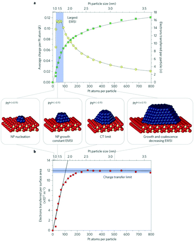 | ||
| Fig. 4 (a) Number of electrons transferred per Pt particle to the ceria support as a function of particle size (green squares). The partial charge per Pt atom reaches a maximum for particles with 30 to 70 atoms (yellow circles). (b) At higher Pt coverage the total amount of transferred charge approaches a limit (charge transfer limit, red squares). The atomic models show schematically the average particle sizes in the different regions. Reproduced with permission from ref. 42. Copyright Springer Nature, 2016. | ||
Interesting, for smaller Pt particles, nucleation occurs at defects and hinders the charge transfer from Pt to ceria. This opens the topic of defective oxide surfaces that will be addressed in the next section. In general, the results reported in ref. 42 show that the charge transfer can be tuned by adjusting the particle size, the particle structure and the chemical properties of the support.
2.2 Defective oxide surfaces
From a general point of view, a defect is an irregularity in the crystal lattice. Due to its structural characteristics, it is associated with new electronic states; often these states appear in the gap of the insulating or semiconducting oxide. One can distinguish two general cases. (1) Defects that introduce new acceptor levels below the conduction band of the material; these levels can act as good electron acceptors, and can contribute to the ionization (or partial oxidation) of deposited metal atoms and clusters. On non-reducible oxides these defect centers can play the same role of the d and f orbitals of TM atoms in reducible oxides: they can trap excess electrons, and favor the charge transfer from a metal nanoparticle to the oxide. Of course, the number of defect centers is orders of magnitude smaller than the number of cations in reducible oxides. (2) In the second scenario, defects introduce new occupied donor levels, sufficiently high in the band gap to lie above the empty (accepting) levels of the adsorbed metal species; when this occurs, electrons can be transferred from the defect to the metal particle. This is often the case when neutral oxygen vacancies are present. Notice that, in order for this charge transfer to occur, it is not necessary that the defect lies on the surface of the material. Sub-surface and even bulk defects may generate donor states in the gap, and the corresponding electrons can be donated to a deposited metal nanoparticle, provided that there is sufficiently high electron mobility.
We illustrate these cases by considering two specific examples. The first one is again the deposition of Na or K atoms or clusters on the surface of a non-reducible oxide, but now in the presence of specific defects able to trap electrons. We have seen above that on the non-defective surface of a simple oxide (e.g. MgO), a K atom (or cluster) is bound by polarization effects with virtually no charge transfer.51,87 In contrast, on-defect rich MgO surfaces a spontaneous ionization of the alkali metal may occur, with a behavior that is reminiscent of that of reducible oxides. This is the case, for instance, of the hydroxyl group (OH).88 Hydroxyls are always present on the surface of an oxide, as they result from the dissociative adsorption of water.89 For reactions occurring at room temperature or slightly above, the oxide surface is partly hydroxylated, and the surface reactivity can be significantly modified compared to a fully dehydroxylated case. Here we discuss cases where OH groups are present in low amounts, and as such can be classified as defects.
The electron trapping ability of OH groups has been demonstrated using EPR by adsorbing Na atoms on fully dehydroxylated and on partly hydroxylated MgO surfaces.88 A MgO polycrystalline sample has been exposed to low doses of Na vapor; Na atoms adsorb on the surface and give rise to an EPR signal, which indicates the presence of an unpaired electron in the Na 3s orbital (Na remains neutral and no CT occurs), Fig. 5. The experiment has been repeated on a partly hydroxylated MgO sample. Surprisingly, the EPR spectrum assumes a completely different shape, and exhibits a line shape that has been unambiguously assigned to electrons trapped near OH groups. What occurs is that Na adsorption is followed by the ionization of the Na atoms (formation of Na+ bound to oxide anions), with the valence electron of Na stabilized at a trapping site formed by a low-coordinated Mg2+ ion and an OH group. In a similar way, also H atoms interacting with the MgO surface can split to form a proton, H+, bound to an O2− ion (formation of an OH− group), and an electron stabilized by the local electrostatic potential near the OH group;90,91 these centers have been named (H+)(e−) centers.92 These experiments show that by simple hydroxylation the chemistry of the MgO surface changes drastically, leading to a spontaneous ionization of Na atoms and clusters, which is not observed on the hydroxyl-free surface.
 | ||
| Fig. 5 Left: Schematic representation of the interaction of a Na atom with an hydroxylated MgO surface. The Na atom dissociates into a Na+ ion stabilized at a reverse corner and an electron trapped near an OH group of the surface where it forms a (H+)(e−) center. Right: EPR spectra of Na atoms deposited on a fully dehydroxylated MgO surface (top) and on a partly hydroxylated MgO surface (bottom).93 Reproduced with permission from ref. 93. Copyright American Chemical Society, 2007. | ||
Other defects, which are able to ionize adsorbed metal species, are cation vacancies, low-coordinated cation sites, and grain boundaries. Electronic structure calculations have shown that grain boundaries at MgO nanocrystals can trap electrons and generate states just below the conduction band, Fig. 6a and b;94 experimental studies on the deposition of Au clusters on MgO/Mo(100) films have shown a tendency for the nanoparticles to nucleate along the dislocations and grain boundaries, Fig. 6c.95 Of course, if excess electrons accumulate at grain boundaries, they can also be transferred to deposited metal nanoparticles. STM experiments have shown the presence of an excess of charge on the supported Au clusters due to their interaction with extended defects.95
 | ||
| Fig. 6 (a) Electrons trapped inside a dislocation in MgO nanocrystals (blue points); and (b) DOS for bulk MgO and MgO grain boundaries with trapped electrons. The dashed lines indicate the positions of the bulk valance-band maximum and conduction-band minimum. I and II label the electronic states associated with the grain boundary. The inset shows electron density isosurfaces for an electron in state I.94 Reproduced with permission from ref. 94. Copyright Nature, 2008. (c) STM topographic image of Au clusters deposited on a 12 ML thick, electron-bombarded MgO/Mo(001) film (100 × 100 nm2). The aggregates preferentially nucleate at the dislocation lines in the film.95 Reproduced with permission from ref. 95. Copyright American Chemical Society, 2010. | ||
The most studied defect center with an ability to transfer electrons to supported metal atoms or nanoparticles is the oxygen vacancy.96 The nature of oxygen vacancies varies a lot from oxide to oxide, but it has in common that the removal of a neutral oxygen leaves behind an electron rich surface. The way these excess electrons are distributed in the solid varies substantially with the nature of the oxide. In ionic oxides such as MgO, CaO, ZrO2, etc., two electrons are trapped at the site created by the missing O atom and stabilized by the strong Madelung field.96,97 In SiO2, a solid characterized by covalent polar ![[triple bond, length as m-dash]](https://www.rsc.org/images/entities/char_e002.gif) Si–O–Si
Si–O–Si![[triple bond, length as m-dash]](https://www.rsc.org/images/entities/char_e002.gif) bonds, the removal of an O atom results in the formation of a direct
bonds, the removal of an O atom results in the formation of a direct ![[triple bond, length as m-dash]](https://www.rsc.org/images/entities/char_e002.gif) Si–Si
Si–Si![[triple bond, length as m-dash]](https://www.rsc.org/images/entities/char_e002.gif) two-center, two-electron, bond, with considerable relaxation of the lattice following oxygen removal.98 In reducible oxides, the electrons associated with the missing O atom are transferred to the empty d or f levels of the M cation (the 3d states of Ti in TiO299 or the 4f states of Ce in CeO2),100,101 with a consequent change in the oxidation state, from M4+ to M3+. This localization leads to a local distortion due to the formation of a small polaron.
two-center, two-electron, bond, with considerable relaxation of the lattice following oxygen removal.98 In reducible oxides, the electrons associated with the missing O atom are transferred to the empty d or f levels of the M cation (the 3d states of Ti in TiO299 or the 4f states of Ce in CeO2),100,101 with a consequent change in the oxidation state, from M4+ to M3+. This localization leads to a local distortion due to the formation of a small polaron.
The presence of O vacancies on the surface (or sub-surface) of the oxide may result in major modifications of the interaction with deposited metals.102,103 This effect has been not only predicted by several theoretical calculations, but also demonstrated experimentally by non-contact AFM, Fig. 7.104 In particular, the forces acting between the metal tip (a PtIr alloy) and the regular oxide anions or oxygen vacancies of a MgO(100) surface have been measured. The presence of vacancies on the surface has been proven by use of an STM tip, and the local forces between the tip and the defect have been measured and compared with the forces between the tip and the regular sites. The interaction energy of the tip is about three times larger with the defect center than with the regular sites. Furthermore, the tip–vacancy interaction acts at relatively long distance from the defect (>5 Å), suggesting that atoms or clusters diffusing on a surface may experience the attractive potential of the defect when they are on its proximity and can then be trapped at the defect center.104 Nucleation and growth start at these specific sites.
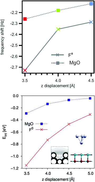 | ||
| Fig. 7 (Top) Resonance frequency shift of a Pt0.9/Ir0.1 STM tip on a regular MgO surface (rectangles) and above an oxygen vacancy (F0) defect site (crosses). The resonance frequency shift is a direct consequence resulting from potential gradients between the tip and the sample. (Bottom) Interaction energy of a Pt4 cluster above the O site of a MgO surface (rectangles) and above a F0 defect center (crosses) calculated by DFT.104 Reproduced with permission from ref. 104. Copyright American Chemical Society, 2010. | ||
Normally, when metal atoms or clusters interact with anion vacancies, charge transfer occurs from the support to the adsorbed metal. The occupied levels of the defect lie high in the gap, and they can be above the Fermi level of the deposited metal particle, inducing electron flow. There is a vast literature on the consequences of this interaction. One measurable effect of the charge transfer is the shift in the vibrational frequency of CO molecules adsorbed on the metal particle. Due to the excess charge accumulated on the metal unit, and the consequent reinforcement of the back-donation mechanism, the CO stretching frequency shifts to the red by about 50 cm−1 for a particle of 1–2 nm diameter,105 as shown for Au nanoparticles deposited on MgO thin films where oxygen vacancies have been created on purpose by electron bombardment.106
The same effect occurs for metal atoms or clusters deposited on reduced TiO2−x or CeO2−x surfaces. Also in this case the defect states (Ti 3d or Ce 4f) lie at relatively high energy in the gap (about 1 eV below the CB in TiO2−x99 and about 2 eV below the 5d band in CeO2−x).107,108 Metals with high work functions promote electron transfer from the defect centers. Since the mobility of trapped electrons in semiconducting oxides is relatively high (the computed barriers for diffusion for TiO2 are of the order of 0.2 eV),109 the nanoparticle does not need to be in direct contact with the vacancy in order to become charged. This effect has been used to design more efficient photo-catalysts where a semiconducting oxide such as TiO2 is interfaced with Au nanoparticles which can act as electron scavengers and reduce the electron–hole recombination, with direct improvement of the photocatalytic activity.110
Of course, the occurrence of charge transfer when a cluster or a nanoparticle is deposited on or near O vacancies depends on the nature of the metal. For instance, in a combined STM and DFT study of Pt and Au monomers, dimers, and trimers deposited on a regular and defective TiO2(101) surface,111 it has been shown that while the Au clusters become negatively charged when deposited on the O vacancies, Pt clusters do not show an appreciable change in their charge state.
An oxide can be doped with an element whose valence is lower than that of the replaced cation (e.g., trivalent La replacing tetravalent Ce to form LaxCe1−xO2);112 such materials are known as “low valence dopants”. These dopants create an “electron deficit”, and one consequence is that the oxygen atoms around the defect have their charge decreased, and therefore bind more weakly to the doped oxide than to the undoped one. The net effect of the low-valent dopants is to make the oxide more reactive in oxidation reactions than the undoped one. According to DFT calculations22 the effect takes place for all oxides and for all low-valent dopants. If doping results in less strongly bound O atoms on the surface, it also favors the formation of O vacancies.
The opposite case is that of a “high-valent dopant”, which replaces a metal cation in the oxide. A typical case is a trivalent Al that replaces a divalent Mg in MgO. Al enters as Al3+ in the crystal when it replaces a Mg2+ ion, and its extra valence electron is transferred to the rest of the lattice. In the absence of defects, the excess electron provided by the Al dopant can only occupy the conduction band of the material, and become delocalized over a large number of Mg ions of the surface.114 This is a rather unlikely process, because the conduction band of MgO is very high in energy and the oxide is non-reducible. However, morphological irregularities or point defects are always present, and have electronic states below the bottom of the conduction band where the excess electron coming from the dopant can be trapped and localized. The oxide becomes rich in excess electrons which can be transferred to an adsorbed metal catalyst if the proper level alignment is achieved.
Similar effects occur by doping simple oxides like MgO or CaO with TM atoms. An example is that of Mo dopants on the growth of gold on a CaO(001) surface (this will be further discussed below, see Section 4.1).115 Mo-doped CaO (CaOMo where about 2% of Mg ions are replaced by Mo) and undoped CaO films have been prepared and their adsorption properties have been studied. By growing a few layers of pure CaO on top of the doped sample, segregation of Mo dopants to the surface has been avoided. In this way, no direct interaction between the Au deposits and the Mo dopants is possible. Deposition of Au at 300 K on pure CaO films results in the formation of 3D gold particles, indicating that gold follows a Volmer–Weber growth, typical of weak adhesion and small or no charge transfer between the metal and the oxide support.116,117 In contrast, on the doped CaOMo films Au forms 2D islands of monolayer height, Fig. 8. This growth mode of Au clusters is typical of strong metal/oxide interactions dominated by charge transfer from the support to gold, and has been demonstrated for Au aggregates on MgO/Ag(100) ultrathin films (see below, Section 3.2).118,119 DFT calculations have shown that Mo2+ (4d4) is an intrinsically unstable species that tends to donate charge to accepting species forming more stable Mo3+ (4d3) or Mo4+ (4d2) cations. The presence of Mo dopants introduces high-lying donor states that efficiently transfer charge to a metal with high electron affinity, such as Au. Thus, doping CaO with Mo results in charge transfer from the doped oxide to the Au particle, at variance with the pure oxide.
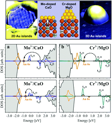 | ||
| Fig. 8 Top: STM topographic images of Mo-doped and Cr-doped MgO(001) films. Bottom: Projected densities of states (DOS) for (a) CaOMo and (b) MgOCr in the presence of a Au atom calculated for two different charge states of the transition metal ion. Charge-transfer processes from the HOMO of the dopant to the Au 6s affinity levels are indicated by arrows.120 Reproduced with permission from ref. 120. Copyright American Chemical Society, 2012. | ||
One should not conclude that every TM dopant behaves in the same way. The final effect depends on the chemical nature of the dopant. For instance, doping MgO with Cr does not lead to any appreciable difference in adsorption properties compared to the pure MgO surface, Fig. 8.120 In both cases, there is no effect of the Cr dopant on the donor properties of the oxide and charge transfer does not occur. The reason for the different behaviors of MgOCr and CaOMo is that while the Mo ion in CaOMo results in excess electrons on the oxide, in MgOCr, Cr3+ species replace Mg2+, leading to the formation of cation vacancies in order to maintain electroneutrality (see above). The occupied Cr3+ states are below or at a similar energy of the Fermi level of Au clusters, which renders electron transfer unfavorable, Fig. 8.120
3 Oxide ultrathin films as model systems
3.1 Preparation
Ultrathin films of insulating materials are attracting increasing interest thanks to their uncommon physico-chemical properties. The field has grown very rapidly after the discovery of materials in the form of single layers. Graphene is the prototype of two-dimensional materials, but several other examples are known.121 Two-dimensional materials have been studied intensively for a variety of potential applications.122,123 Thin layers of oxide materials, however, have been used in various technologies in the last few decades. For instance, ultrathin silicon dioxide films have been the basis of metal oxide field effect transistors;124 to a large extent the microelectronic revolution is based on the excellent properties of thin SiO2 films grown on silicon. Thin oxide layers form under reactive conditions when metals are exposed to oxidizing conditions; the formation of passive films guarantees corrosion protection of metals.125,126 Today two-dimensional oxides are studied as ultrathin capacitors,127 for solar energy materials,128 for magnetoresistance sensors,129etc.130In the last two decades, oxide ultrathin films have become interesting also in heterogeneous catalysis. They have been prepared as model systems to develop concepts of electronic/geometric structure–reactivity relations to be transferred to the properties of real catalysts. Those ultrathin films allow the application of electron spectroscopies and scanning probe microscopies (SPM) to aim at their characterization at the atomic level.131–135 Specific techniques have been developed to grow epitaxial oxide films, deposit metal nanoclusters, and study their chemistry under controlled conditions. In general, while ultrathin oxide films may closely resemble the corresponding bulk counterparts, other ultrathin film oxides exhibit completely different properties. Particularly interesting in this context is the possibility of selectively charging atomic or molecular species adsorbed on an oxide ultrathin film.136,137 Electrons may tunnel through the insulating thin layer, leading to charged surface species supported on oxide thin films. The charge transfer then results in completely different chemistry and catalytic activity.
A number of studies have indicated that non-reducible oxides may be especially suitable for thin film growth116,138–143 when a well-adapted metal support to allow for epitaxial growth was used. MgO, CaO, Al2O3 and SiO2 are examples. Typically, ultrahigh vacuum conditions and physical vapor deposition in an oxygen atmosphere are used so that the material is free of any contaminant,140 which for reliable experimental studies is a non-debatable prerequisite. Fig. 9 shows for MgO(100) grown on Ag(100) that those films exhibit the geometric characteristics of their bulk counterparts and even the physical and chemical properties are very similar if those films are grown to a certain thickness. Electron diffraction (low energy electron diffraction, LEED) and electron spectroscopies (electron energy loss spectroscopy, EELS, and ultraviolet photoelectron spectroscopy, UPS) for films of various thicknesses indicate that the properties, such as geometric structure, phononic properties and even the band gap of 6 eV (differential conductance measurements using STM), for films of a few monolayers correspond closely to those of a MgO(100) single crystal.141,142,144–148 Density functional calculations support the experimental results.149 The defect free MgO surface150,151 is quite inert, at variance with a defect rich surface (see Section 2.2), and the defect density may be controlled by the preparation conditions, induced by the STM tips by operation at high voltages and high currents, or by the choice of the metal substrate.152 Mo(100), for example, exhibits a larger misfit to MgO, which favors the formation of defects, in particular steps and kinks as well as point defects, such as color centers (oxygen vacancies). Those point defects are traps for electrons, which may be transferred to adsorbates (metal atoms or molecules, see Section 2.2.1).153–155 The point defects (color centers) come in different flavors, depending on how many electrons have been trapped. They are called F0, F+ or F2+ centers for two, one and no electrons trapped. A combination of scanning tunneling spectroscopy and high-resolution Kelvin probe force microscopy allows the identification of the various color centers.104,156 It is found that most of them but not all are localized at kinks and steps, since the energetic cost for its formation is considerably lower than that on terraces.
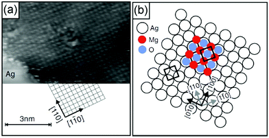 | ||
| Fig. 9 (a) Atomic resolution indicating the lattice orientation of the substrate (It = 2 pA, Vt = 30 mV). Subsequently, atomic resolution of an MgO film surface has been achieved by site specific dynamic force microscopy (AFM).157 (b) Growth model of MgO/Ag(001). Illustration of the most favorable configuration: Mg-atoms occupy hollow sites, i.e., they continue the Ag fcc lattice (lattice constant a = 0.409 nm), and O-atoms occupy on top sites. The Ag(001) surface unit cell is indicated. From ref. 149 and 158. | ||
As stated above, the films are prepared by physical vapor deposition onto a metal substrate, followed by an annealing step to order the surface structure. Depending on the annealing temperature, diffusion of metal atoms (dopants) from the substrate into the oxide film has been observed. This has been studied in detail for CaO(100) films grown on top of a Mo(100) surface. The state of the dopant may be probed using XPS, whereby the depth distribution of the dopants may be analyzed using angle dependent XPS or photon energy dependent spectra via synchrotron radiation studies via an effective variation of the electron escape depth.120,159–161 Another way to bring the dopant into the film is successive evaporation of a film of a given thickness, followed by the evaporation of the dopant material and a second controlled film deposition step to bury the dopant. This allows for a controlled deposition of the dopant at a given depth below the oxide surface.
Another example for an oxide film with great potential in model catalyst preparation is SiO2.162,163 Ultra-thin silica films have been grown using similar recipes to those for MgO on a number of metal single crystal surfaces. Depending on the oxygen affinity of the metal substrate, either single layers directly bound to the metal substrate or bi-layer films, only van der Waals bound to the substrate, or both on the same substrate, have been prepared.164,165 In particular, bilayer films were thoroughly studied with respect to their structure with a particular emphasis on the analysis of crystalline and amorphous structures. Ru(0001) is the metal substrate on which both monolayer and bilayer films have been prepared. They have been experimentally studied and characterized using STM, LEED, infrared reflection absorption spectroscopy (IRAS) and XPS. Fig. 10 shows electron diffraction patterns and scanning tunneling images of the films together with structural models, which have been established on the basis of the experimental data in combination with density functional calculations.
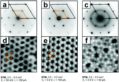 | ||
| Fig. 10 Low energy electron diffraction diagrams and STM topographic images of the respective systems, i.e. (a) and (d) a silica monolayer on Ru(0001), SiO2,5/Ru(0001), (b) and (e) a crystalline bilayer and (c) and (f) a vitreous (amorphous) bilayer, SiO2/Ru(0001).163,166 Adapted with permission from ref. 166. Copyright American Chemical Society, 2012. | ||
The structural principle is based on corner-connected SiO4-tetrahedra forming a two-dimensional structure of six-membered rings. In the mono-layer films one corner of the SiO4-tehedra is directly bound to the metal substrate, while in the bi-layer films a second, flipped layer of corner-connected SiO4-tetrahedra is bound from below directly to the top layer forming Si–O–Si bonds between the layers. In contrast to the monolayer, the bi-layer exhibits perfect SiO2 stoichiometry. Since all the constituting atoms are valence saturated, the bi-layer film is only bound to the metal by dispersion forces. This bi-layer film exists both in a crystalline and in an amorphous phase as is convincingly demonstrated using scanning tunneling images. It represents the first example of an amorphous oxide film, where the structure is identified down to the atomic level.167 It proves the model for amorphous silica proposed by Zachariasen in 1932.168 He proposed a model where the SiO4-tetrahedra are still corner connected but form rings of different sizes ranging from 4-membered to 9-membered rings. Detailed investigations prove that the bi-layer film corresponds perfectly to the Zachariasen model, and may also be used in comparison to 3-dimensional silica. With respect to the present review it is important to mention that the amorphous bi-layer represents a model for an amorphous silica support, a material often used to fabricate real catalytic materials. Examples are heterogenized homogeneous catalysts, where metal complexes are bound to an amorphous silica substrate. An industrially important example is the Phillips catalyst for ethylene polymerization.169–172 In this system, chromium atoms are bound to the silica, and the exact bonding situation is claimed to be relevant to understand the detailed mechanism of the polymerization reaction.173–181
This brings us to another aspect: in order to bind metal atoms, in particular to amorphous silica, the film has to be hydroxylated. This turns out to demand a special methodology due to the stability of the film. Only via electron bombardment in the presence of water does hydroxylation turn out to be possible.182,183 For details we refer to the original literature. However, oxide film hydroxylation, in general, is an important aspect also, and in particular with respect to MgO.184 In the latter case, hydroxylation is important depending on the chemical nature of the metal bound to the oxide surface. If one attempts to understand the basic mechanisms of wet impregnation techniques, it is obviously crucial to investigate the bonding not only to pure oxide surfaces, but also to those hydroxylated. In general, one needs to realize that understanding chemical modification of oxide surfaces is prerequisite to be able to mimic the complexity of real catalyst systems.185
Once the oxide films have been prepared, the final step in the preparation of a metal–oxide supported model catalyst system is the deposition of the metal particle.116 Basically two different approaches have been used. One, the simpler technique, is the diffusion-controlled growth of particles after physical vapor deposition of a given metal.116,139,140,186 The other, more technically demanding one, is deposition of size-selected clusters prepared by laser vaporization of the chosen metal in a He-atmosphere or by He-ion sputtering and subsequent mass-selection in a quadrupole mass filter.140,187,188 In the following sub-section we will discuss a number of examples of metal nano-particles on ultrathin oxide films, also with respect to charge control.
3.2 Nano-particles on ultrathin oxide films
Individual Pd atoms on an ultrathin alumina were imaged first by Nilius et al. in 2003,189 after theoretical predictions had been published for alumina and MgO. Those theory papers predicted a positive charge for the Pd on alumina and a neutral Pd atom for MgO.190,191 Experimentally, evidence for the charge state of the metal atom could not be provided. Clear experimental indications on the charge state of individual metal atoms on thin films were provided using STM studies on Au atoms deposited on a NaCl films grown on Cu single crystals by applying voltage pulses to the tip, and thus changing the charge state of the atom.192,193 On oxide films clear evidence was provided via STM and theory194,195 for negatively Au atoms and neutral Pd atoms on MgO(100) in comparison with density functional calculations. The Pd atoms reside on the O ions, while negatively charged Au atoms reside on Mg or on hollow sites.194,195Fig. 11 shows a comparison of the distribution of Au atoms in Fig. 11a and Pd atoms in Fig. 11b. Due to the negative charge the Au atoms carry, and the associated Coulomb repulsion to other negatively charged species, the Au atoms repel each other, which leads to the observed non-statistical spatial distribution, while the neutral Pd atoms clearly exhibit a statistical distribution.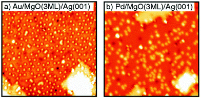 | ||
| Fig. 11 STM images (30 × 30 nm2) of (a) Au atoms (θ = 2.9% ML Au) adsorbed on 3 ML thin MgO films (Vs = 0.5 V, It = 11 pA); and (b) Pd atoms (θ = 2.3% ML Pd) adsorbed on 3 ML thin MgO films (Vs = 0.2 V, It = 13 pA). Reprinted with permission from ref. 195. Copyright 2007 by the American Physical Society. | ||
A series of studies on metal atom aggregates have been reported. The first study to experimentally determine charge transfer by STM conductance imaging of metal aggregates was reported in 2008 in combination with a computational effort by the Sauer group.37 As shown in Fig. 12 the conductance images of linear Au chains on alumina/NiAl(110) with varying lengths represent the quantum states of the systems created by the Au 6s electrons.
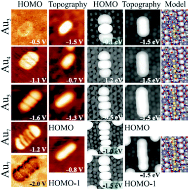 | ||
| Fig. 12 Experimental conductance images of the Au chain states representing the ground state and calculated HOMO (highest occupied molecular orbital) shapes, topographies, and model structures for Au3, Au4, Au5, and Au7 chains. Images are 5.0 × 5.0 nm2 in size. For the Au7 chain, a second state at higher imaging voltage in addition to the HOMO−1 are shown. Measured chain lengths are 0.9 nm, 1.2 nm, 1.5 nm, and 2.2 nm; calculated distances between the first and last chain atoms amount to 0.53, 0.78, 1.05, and 1.55 nm. To compare theoretical to experimental lengths, 0.2 to 0.3 nm should be added to both chain sides to account for the diffusivity of the 1D orbitals. Reprinted with permission from ref. 37. Copyright 2008 by the American Physical Society. | ||
Identifying the states below and above the Fermi energy and knowing the number of atoms involved in the Au chain allow counting the number of electrons in the chain. The idea is to use the concept of a particle-in-a-box and to count the nodes in the electron densities of states as a function of energy. This leads in the case of the Au7 chain to the result that three electrons must have been transferred in addition to the electrons provided by the Au atoms in the chain. An important prerequisite is, of course, that the number of atoms is known, which restricts a detailed analysis to relatively small aggregates. Another example for a somewhat larger two-dimensional aggregate is shown in Fig. 13.38
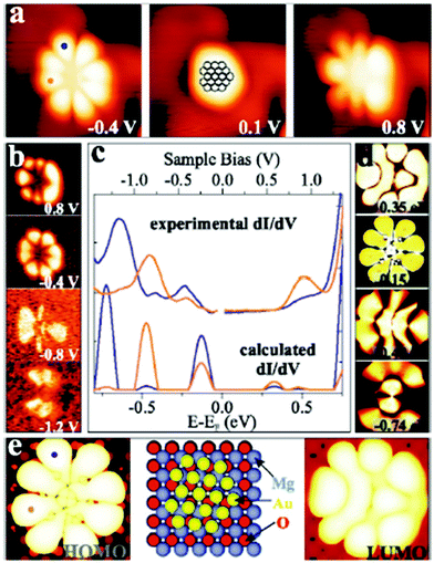 | ||
| Fig. 13 (a) STM topographic and (b) conductance images of a Au18 cluster on 2 ML MgO/Ag(001) (It = 5 pA, 3.9 × 3.9 nm2) in comparison with simulated (d) conductance and (e) topographic images (2.0 × 2.0 nm2) and a structure model. (c) Experimental and simulated dI/dV spectra recorded at the blue and orange dots marked on the cluster in (a) and (e). Reprinted with permission from ref. 38. Copyright 2009 by the American Physical Society. | ||
This figure is based on an experimental study by Lin et al.,38 in collaboration with the Häkkinen group, providing the theoretical input. A Au18 cluster has been identified, and by applying the same procedure as outlined above for the linear chain, but adapted here to the two-dimensionality of the object it is concluded that 4 extra electrons have been transferred to the flat Au particle. In an attempt to generalize this procedure to larger objects of 100 atoms or more and arbitrary shapes it is found, as alluded to above, that a strict purely experimentally based analysis is difficult. However, based on calculations in comparison to experiments on larger islands it was noticed that the extra charge tends to be localized at the rim of the object.39 This is documented in Fig. 14 where STM topographic images of two-dimensional larger Au islands are shown.
 | ||
| Fig. 14 (a) Conductance spectra recorded on a kink and a step position of the island shown in the inset. The bias set point was +0.5 V. The locally increased density of states at the cluster rim is clearly observed in (a) and (b), indicating the presence of a negatively charged 2D-Au cluster. Reprinted with permission from ref. 39. Copyright 2010 by the American Physical Society. | ||
Fig. 14b presents the filled and empty states of a Au island and illustrates the localization at the rim of the nano-particle. We note here that the electron localization at the rim occurs through electron transfer from the metal substrate, while the mixing of the electronic states of the metal underneath the film and the metal nano-particle on top of the film is negligible. Are there conventional ways by XPS to verify the negative charge on the particles? To answer this question, an Auger parameter study was carried out for flat Au particles.181 Wagner established the Auger parameter concept and showed that the changes in the difference between the binding energies (BEs) of XPS and kinetic energies (KEs) of Auger peaks from a given atom are related to changes in the final state, i.e. the ion state, of the atom exclusively via the following equation:196
| Δα = Δ(BEXPS + KEAuger) = 2ΔR, | (2) |
| Δβ = Δ[2EB(i) − EB(j) + EKin(jii)] = 2ΔRi. | (3) |
This definition does no longer require the assumption of equal relaxation for all levels. Details are described in the literature.181,199,200 Since the relaxation energy may be calculated from this relation in a straightforward manner and the difference in binding energy is the difference between the initial state shifts, i.e. the difference in the Koopmans energies of the involved level, the initial state shift may be extracted. This shift is directly correlated with the charge the core level experiences. Fig. 15 compiles the data for the Au nano-particles on MgO(100)/Ag(100) as a function temperature.
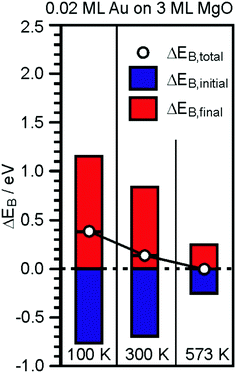 | ||
| Fig. 15 Graphical representation of the EB-shifts derived from XPS and Auger measurements for 0.2 ML Au on 30 ML MgO(001)/Ag(001) with reference to Au(111).181 | ||
The temperature has been varied because it has been learned that at a temperature higher than 550 K the particles start to lose their flat morphology. Clearly, the initial state shifts of the Au particles are strong and negative, consistent with the negative charge on the Au particles. However, the final state shifts are even bigger and overcompensate for the initial state shifts, thus leading to an observed chemical shift, which, would it be taken to represent the charge state, would have led to wrong conclusions. In comparison to the Au particles on the ultrathin MgO film, a similar study has been performed for a similar amount of Au deposited on a thick (60 layers) MgO film, representing bulk MgO.181,201 The particles exhibit a three-dimensional morphology, which was predicted by computations to not exhibit strong charge transfer to the Au particles,118 and thus no reactivity towards CO2 (see below). The negative initial state shifts are missing and the results are consistent, indicating that the presented approach to determine charge transfer is valid and corroborates theory.
Very recently, Calaza et al.202 were able to correlate the electron localization at the rim of Au nanoparticles with chemical reactivity. Carbon dioxide was used as a probe. A set of STM topographic images (a–c) of the reactive system together with differential conductance curves as a function of bias voltage (d) are shown in Fig. 16.
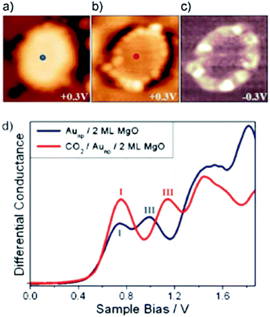 | ||
| Fig. 16 (a) STM topographic images of (a) a pristine planar Au cluster and (b) after exposure to CO2 (scan size 8.0 × 8.0 nm2, 50 pA). The Au clusters were prepared by evaporating Au on MgO mono- or bilayer films at 300 K. Subsequently, the sample was exposed to 10–15 L CO2 in a temperature range from 220 to 250 K. Molecules at the cluster perimeter in (b) become visible only when scanning at bias voltages between −0.5 and +0.5 V. (c) Corresponding dI/dV map, displaying the high localization of electron density at the negatively charged cluster rim. (d) dI/dV spectra recorded at the center of the clusters shown in (a) (blue) and (b) (red). The positions of the first (I) and third (III) quantum well states in both spectra are indicated. Note the energy shift towards higher energy of the internal energy scale of the cluster which is compatible with a CO2 induced decrease of the electron potential well formed by the Au island. Reprinted with permission from ref. 202. Copyright 2015 Wiley-VCH. | ||
The visible protrusions have been identified as oxalate anions (C2O42−) via infrared spectroscopy. This may sound surprising! However, while CO2 is a thermodynamically very stable molecule requiring 0.6 eV to transfer an electron to form a CO2-anion, a CO2-dimer, for example, forms an anion exothermically with a gain in energy of approximately 0.9 eV.202–204 The barrier for formation is, of course, the energy to bend the linear molecule. This observation is fully in line with the observed reactivity of CO2 on alkali (i.e. electron enriched) metal surfaces.205 Clearly, the reactivity is linked to the electron localization at the rim of the nano-particle. The fact that this may be directly observed using scanning probe techniques is a consequence of the flat morphology of the nano-particle. Had the particles been three-dimensional with a regular aspect ratio observed in real catalysts, this would not have possible, as attempts to directly image reactivity at the rim have failed so far.40 The present system allows for an even more in depth analysis of the electronic structure. As indicated in Fig. 16d, the quantum well states of the Au nano-particles shift as the molecules cover the nano-particle rim. A detailed analysis206,207 shows that the observed shifts are compatible with a situation where the electrons occupying Au quantum well states are energetically shifted to higher values because of the presence of the extra negative charge on the molecules at the rim. This observation reveals how molecular adsorption modifies the properties of metal nano-particles, a topic of importance in heterogeneous catalysis.
At this point, a word about inverse catalysts appears to be in order.208,209 When one deals with reactivity at oxide–metal interfaces, so far we have chosen the approach to place the metal nano-particle on top of an oxide film in order to mimic the situation encountered in real catalysts. Another option chosen by some researchers is to create an oxide film on top of a metal surface (representing the metal the nano-particle is made of) and not fully cover the metal surface, so as to leave the oxide–metal interface open and accessible.210–212 A schematic is shown in Fig. 17.
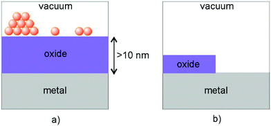 | ||
| Fig. 17 Schematic illustration of (a) a “regular” model system and (b) one representing an “inverse” catalyst. Adapted with permission from ref. 208. Copyright 2016 American Chemical Society. | ||
Some researchers call this an inverse catalyst (inverse with respect to metal-particles on oxides) and claim that this allows interrogation of the interface in the same way as for the metal particle on top of the oxide support. This nomenclature is somewhat misleading, as it implies that for the interface it does not matter whether one investigates metals on oxides or oxides on metals. Obviously, this is incorrect, because the details at the interface will be rather different. Still those investigations are useful in their own right, as they are encountered in specific situations in catalysis, in particular, in so-called SMSI situations described in the Introduction,26,213–220 as we will see in the final chapter.208
Having raised this issue of whether the support–metal interface is properly represented, some more considerations are appropriate. One specific comment concerns here the investigation of compound nano-particles on metal substrates, where the metal only represents a platform to investigate the compound particle per se. We discuss here an example put forward by the Besenbacher group investigating MoS2 nano-particles on Au substrates.221 As shown in Fig. 18 they were able to present beautiful atomically resolved STM images revealing the triangular morphology of the particle.
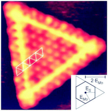 | ||
| Fig. 18 An atom-resolved STM image (scan size 4.1 × 4.1 nm2, It = 1.28 nA, Vt = 5.2 mV) of a triangularly shaped single-layer MoS2 nanocluster. The grid shows the registry of the edge atoms relative to those in the basal plane of the MoS2 triangle. The inset shows a Wulff construction of the MoS2 crystal. EMo and ES denote the free energies for the Mo and S edges, respectively (from ref. 221). The lines of highly increased contrast following the edges of the MoS2 triangles were shown to originate from one-dimensional metallic edge states in MoS2. Reprinted with permission from ref. 222. Copyright 2001 by the American Physical Society. | ||
The geometric parameters deduced from the STM images are fully consistent with the geometric parameters of the basal plane of bulk MoS2. However, the hexagonal basal plane would have suggested hexagonal nano-particles, while triangular particles are observed. This implies that the different edge terminations exhibit different stabilities. In comparison with calculations it was found that the observed edge structure is only obtained when the stoichiometry on the edges changes, in the sense that only one S atom is bound to the Mo edge atom. This is, of course, important to understand those MoS2 nano-particles. However, the influence of the Au template (substrate) needs to be considered as well. In the spirit of the inverse catalyst approach, we must ask the question whether the extended Au substrate does not influence the morphology of the sulfide-nano-particle via direct coupling of the electronic structure of the Au with the sulfur of the MoS2. Given the strong affinity of sulfur to Au, this is not unlikely.
3.3 Polaronic distortion: a response to the formation of charged adsorbates
The study of charge transfer phenomena occurring on oxide ultrathin films has shown that the effect is accompanied by non-negligible structural relaxation. The geometrical response to the charge transfer turns out to be essential for the stabilization of the charged species and, in general, for the properties of the films. Ultrathin films possess a structural flexibility, which has no correspondence on bulk surfaces. In this section we will provide some examples to discuss the effect and demonstrate its role in charge transfer properties and even catalytic reactions.As we mentioned above, gold atoms exhibit completely different adsorption properties when deposited on bulk MgO or on an ultrathin MgO film supported on a metal: while they remain neutral on MgO(100), they become negatively charged on MgO/Mo(100) or MgO/Ag(100) ultrathin films.194,195 The net charge transfer takes place via spontaneous electron tunneling, provided that the film thickness remains below the mean-free paths of electrons. This effect is always accompanied by a structural relaxation of the films.
As an example we consider a Ag atom adsorbed on MgO/Mo(100) films.223 Here Ag becomes a full anion according to DFT calculations, which also show a non-negligible local relaxation in the MgO top layer. This can be quantified by the change in vertical distance, Δz, of a given ion of the surface before and after adsorption of the Ag atom, Table 1. If the Ag atom is adsorbed on a bare MgO(100) surface (here represented by 3 ML MgO films), the displacements of the O or Mg ions to which Ag is bound, Δz, and of the first neighbors are very small (<0.02 Å in absolute values). If the Ag is now adsorbed on MgO(3 ML)/Ag(100) films the displacements become substantial, Δz = 0.1–0.2 Å, Table 1: in particular, when Ag is adsorbed on top of an O2− ion the downward displacement is 0.08 Å; the neighboring Mg cations move up by about the same amount. If, however, the negatively charged Ag atom is positioned on top of a Mg cation, the displacement of this ion from the MgO top layer is rather large, 0.23 Å, Table 1.
| On top of O | On top of Mg | ||||
|---|---|---|---|---|---|
| ΔzO (Å) | ΔzMg (Å) | ΔzO (Å) | ΔzMg (Å) | ||
| Ag1 on | MgO(100) | +0.01 | +0.02 | −0.02 | −0.01 |
| Ag1 on | MgO/Mo(100) | −0.08 | +0.09 | −0.03 | +0.23 |
| Au1 on | MgO(100) | −0.04 | +0.03 | −0.02 | +0.01 |
| Au1 on | MgO/Mo(100) | −0.20 | +0.15 | −0.03 | +0.36 |
The effect is even more pronounced for Au. This is shown by the Au–MgO distances: on MgO/Mo(100) films the Au–O2− distance (2.76 Å) is 0.52 Å longer than that on the bare MgO(100) surface, and the Au–Mg distance (2.57 Å) is 0.13 Å shorter. Thus, the formation of a Au anion is accompanied by a large surface relaxation, at variance with Au on MgO(100). On MgO/Mo(100) 3 ML films, Au atom adsorption on Mg is accompanied by an outward displacement of the cation by 0.36 Å; Au adsorption on O induces a downward displacement of −0.20 Å (and an outward movement of the neighboring Mg cations by 0.15 Å, Table 1).
These geometrical relaxations are typical of the formation of a small polaron in an insulating material and provide an important contribution to the stabilization of the adsorbed species. To prove this, a computational experiment has been designed where the MgO ultrathin film is not allowed to relax in response to the adsorption of a Au (or Ag) atom. Interestingly, if no relaxation is allowed, the charge transfer is suppressed and the formation of the Au− species is not observed. Hence, the charge transfer is a direct consequence of the structural deformation of the two-dimensional oxide in response to charge localization on the Au adsorbate.
The formation of negatively charged adsorbates is not restricted to Au. Molecular oxygen can induce an electron transfer and form superoxo species. The formation of O2− species on MgO/Mo(100) films exposed to oxygen has been predicted theoretically224 and confirmed by low temperature EPR spectra.225 The EPR study shows that for films containing 15 ML of MgO, the EPR signal disappears, indicating the suppression of the electron transfer if the oxide film becomes too thick and in full agreement with the model of charge transfer via electron tunneling. Particularly interesting for the present discussion is the analysis of the g-tensor of the O2− species formed on MgO/Mo(100) films, Table 2. This, in fact, provides experimental evidence that indeed the MgO film undergoes a polaronic distortion in response to the formation of the O2− species.
| Method | Site | g xx | g yy | g zz | Δgzz | |
|---|---|---|---|---|---|---|
| MgO powders | Exp. | Terrace | 2.002 | 2.008 | 2.091 | 0.000 |
| MgO powders | Exp. | Edge | 2.002 | 2.008 | 2.077 | −0.014 |
| MgO/Mo(100) | Exp. | Terrace | 2.002 | 2.012 | 2.072 | −0.019 |
| MgO(100) | Theory | Terrace | 2.0022 | 2.0092 | 2.0639 | 0.0000 |
| MgO(100) | Theory | Edge | 2.0021 | 2.0096 | 2.0527 | −0.0112 |
| MgO/Mo(100) | Theory | Terrace | 2.0025 | 2.0093 | 2.0560 | −0.0089 |
The EPR experiments, performed under ultrahigh vacuum conditions at 40 K on a 4 ML thick MgO/Mo(100) film, give the following components of the g-tensor: gxx = 2.002, gyy = 2.012, and gzz = 2.072. Similar measurements exist for O2− species formed on the surfaces of MgO polycrystalline materials,226–228 where the superoxo species forms by interaction of O2 with electron-rich, defective sites at the surface of the material. Thus, it is possible to compare the values of the g-tensor found on the thin MgO/Mo(100) films with those obtained on the surfaces of MgO powders. The x- and y-components of the tensor are not too different, while a significantly larger z-component is found on powders compared to thin films: gzz = 2.091 on the (100) terrace sites of MgO powders, and gzz = 2.072 on the terrace sites of MgO/Mo(100), Table 2.
These differences, small but significant, can be explained with the help of theory. The g-tensor has been computed for an O2− radical adsorbed on a MgO cluster modeling the MgO(100) surface, Table 2. With respect to the measurement on the MgO powder samples, the gxx and gyy components are well reproduced, while the gzz component is slightly underestimated in the calculation (the gzz component is systematically underestimated in calculations). However, what is relevant is the trend found comparing the computed g-tensors of O2− on terrace, Mg5c, and edge, Mg4c, sites. There is a reduction of the gzz component, Δgzz, by lowering the coordination number of the Mg ion, Table 2. Now we come to the implications of this result for the discussion of the polaronic distortion in thin films. The value of the gzz tensor measured for the MgO/Mo(100) thin films is closer to that measured on MgO powders and assigned to Mg ions at low-coordinated edge sites. But it can be demonstrated that on the thin MgO/Mo(100) films O2− forms on the flat terrace sites, not on the edges. So why are the gzz values similar in the two cases? The answer is the polaronic distortion. A calculation which includes the polaronic distortion of the MgO/Mo(100) thin film shows in fact a considerably reduced gzz component, as observed experimentally, Table 2.225
To better understand this effect, it should be reminded that the shift of the gzz component from the free electron value is given by gzz = ge + 2[λ2/(λ2 + Δ2)]1/2, where λ is the spin–orbit coupling constant and Δ = 2πyg − 2πxg is the strength of the local electric field. A more exposed cation, as on the edge sites of the MgO powders, or on the terrace sites of the MgO/Mo(100) thin films when the polaronic distortion is present, leads to a reduction of gzz. This is exactly what is found both in theory and in experiment. The smaller value of gzz for O2− on the MgO thin film is thus direct proof of the occurrence of a polaronic distortion.
Another confirmation of the structural flexibility of oxide ultrathin films comes from the study of XPS line broadening.229 XPS is usually based on the analysis of the areas and positions of photoemission peaks. Vibrational excitations lead to broadening in XPS, connected to the change in the nuclear geometry at equilibrium between the initial ground state and the final excited or ionized state. Since the flexibility of thin oxide layers is connected to the phonon structure of the material, one can look at the broadening in photoelectron spectra to investigate the vibrational properties. In particular, changes in the initial-state polaronic distortion can affect the final-state changes in bond length. Comparing the line widths of MgO ionizations in single crystals or thick MgO films and an ultrathin MgO/Ag(100) film (Fig. 19), it has been possible to obtain a direct indication of the changes in structural flexibility.
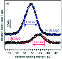 | ||
| Fig. 19 Experimental Mg 2p XPS spectra of 14 ML and 1 ML MgO/Ag(100). Adapted from ref. 229. Copyright 2011 Wiley-VCH. | ||
Fig. 19 shows the experimental Mg 2p XPS spectra of 1 and 14 ML MgO/Ag(100) films. For 1 ML MgO/Ag(100) the full width at half maximum (FWHM) of the Mg 2p peak is 1.45 eV; this becomes approximately 1.60 eV for 10 ML and thicker MgO films. The reduction in the broadening for the thin layer is predicted by theory based on pure Frank–Condon broadening. The Frank–Condon broadening for 1 ML MgO differs from those of thick MgO films (bulk-like) because the equilibrium Mg–O distance, re, is different for bulk and monolayer MgO; this is true for both the ground state and the 2p hole potential curves. Also the curvatures of these potential curves, as measured by ωe, are different between bulk and monolayer MgO, and provide a measure of the softness of the phonon modes of the 2D oxide.
The softness of the ultrathin films is not restricted to MgO. Going to SiO2, for instance, other pieces of evidence of the softness of the thin films come from the study of their adsorption properties. Crystalline SiO2/Mo(112) monolayer films have been investigated in detail by experiment and theory.230–232 The structure of these films has been described in Section 3.1. The film consists of hexagonal rings interrupted by eight-membered rings along line defects. Spontaneous charging of deposited gold does not occur on pristine SiO2/Mo(112) films: both experiments and calculations show that gold atoms interact very weakly with the surface, diffuse and aggregate to form Au nanoparticles in correspondence to the line defects.233,234 However, a possible way to modify the film reactivity is to dope the system with alkali metal atoms which form M+ ions stabilized above the silica film or at the SiO2–Mo(112) interface, depending on the size. For instance, Li atoms diffuse spontaneously through the six-member rings of the silica film to the interface where they form stable Li+ ions. The interface Li ions cannot interact directly with the deposited Au atoms which are adsorbed on the silica surface. The presence of Li+ ions lowers substantially the work function Φ (up to 1 eV for a full coverage θ = 1 corresponding to one interface Li atom per silica ring). Au atoms deposited on the Li-doped SiO2/Mo(112) film show properties that differ completely from those of the corresponding undoped system.235,236 On some surface sites the Au atom becomes strongly bound, by 1.33 eV, and negatively charged (−0.80 e). With the help of STM images it has been possible to verify that the Au atoms are effectively stabilized above these specific sites of the film. Notice that the charge transfer, and hence the stabilization of Au−, is possible only on these specific adsorption sites:237 this is connected to the strong polaronic distortion which stabilizes the charged state of the Au− anion. DFT calculations show that on these sites the O atom of the top layer relaxes towards the Mo surface by about 0.85 Å, while the two adjacent Si atoms move towards the Au anion by about 0.1 Å. This relaxation strongly stabilizes the 6s level of Au, which becomes doubly occupied with the formation of Au−. As for MgO/Ag(100), if the polaronic distortion is not allowed, then the charge transfer does not take place.
3.4 Electrostatic origin of rumpling in supported oxide thin films
Structural relaxation in supported oxide films can be substantial also without the presence of adsorbed species. In this case the relaxation is not local and it involves the entire film. It can be measured by the extent of rumpling, defined as the separation between the atomic planes of cations and anions of a monolayer. In general, the rumpling for unsupported monolayers is negligible;238 however, this can become substantial if the oxide film is deposited on a metal, and depends on the electronic properties of the metal substrate.239 The occurrence of charge transfer at the metal/oxide interface generates an electric field which, in turn, causes the rumpling of the oxide film. If the oxide film is deposited on a metal with high electronegativity (high work function), charge is transferred from the oxide to the support; in this case the anions in the oxide layer are pushed outwards, Fig. 20a, for electrostatic reasons.240 Of course, the opposite is also true. A substrate with low electronegativity (small work function) favors electron flow towards the oxide, and in this case it is the oxide cations that are displaced outwards, Fig. 20b. In this respect, the rumpling in the thin supported film is simply the structural response to the charge transfer occurring at the metal/oxide interface.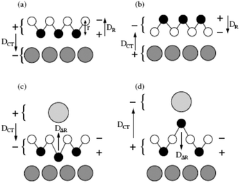 | ||
| Fig. 20 (a and b) Schematic representations of the coupling between dipole moments due to charge transfer at the interface (DCT) and due to rumpling (DR) in oxide monolayers (black circles = cations, white circles = anions) deposited on a metal substrate (large gray circles). (c and d) Schematic representations of “direct” (c) and “flipped” (d) adsorption modes of an adatom (large circle) on a supported oxide film. Direct adsorption mode: the polaronic-like distortion induced by the adatom increases the rumpling (distance between planes of anions and cations); flipped adsorption mode: the distortion reduces the rumpling. Dipole moments due to the charging of the adatom (DCT) and to the adsorption-induced structural distortion (DR) are plotted schematically with arrows. Adapted with permission from ref. 240. Copyright 2009 by the American Physical Society. | ||
The rumpling in the oxide layer generates a dipole (DR) with the opposite sign with respect to that due to charge transfer at the interface (DCT). The two effects go in opposite directions. This is well demonstrated by DFT calculations showing that MgO monolayers interfaced with electropositive metals (Al and Mg) induce electron transfer from the metal to the oxide and a negative rumpling (oxygen closer to the metal surface, Fig. 20b); MgO monolayers deposited on metals with large work functions (Ag, Mo and Pt) induce electron transfer from the oxide to the metal, and a positive rumpling (oxygen relaxes outwards), Fig. 20a.
In a similar way, the adsorption of an atom, a molecule or a small cluster, when accompanied by charge transfer, induces a polaronic distortion that can be rationalized in terms of compensation of surface dipoles. In fact, the local relaxation induced by the charge transfer generates a dipole moment which counteracts that due to the charge transfer, Fig. 20c and d. As a consequence, on structurally soft oxide monolayers the same adsorbed species can exist in two opposite charge states, stabilized by different displacements of the ions in the films, Fig. 20c and d.
This effect has been demonstrated for the case of Au atoms adsorbed on FeO(111)/Pt(111) ultrathin films.241 These films exhibit a periodic variation of the interface structure due to the lattice mismatch between FeO(111) and Pt(111), with the formation of a Moiré superlattice. DFT calculations show that a Au atom deposited on FeO(111)/Pt(111) becomes negatively charged if the rumpling is locally reversed with respect to the clean surface, with an outward displacement of a Fe atom, Fig. 21a.241 In contrast, the Au atom becomes positively charged if the oxygens relax outwards, and the Fe ions relax towards the Pt surface, Fig. 21b. Of the two configurations, charge 1− or charge 1+, only that corresponding the positively charged Au has been observed experimentally.241 The fact that the other configuration has never been observed could be due to the presence of a kinetic barrier to reverse the local rumpling.
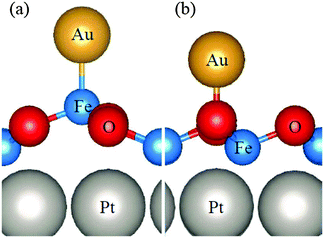 | ||
| Fig. 21 Side views of a Au atom adsorbed on the FeO(111)/Pt(111) substrate: (a) flipped top-Fe configuration (negatively charged Au) and (b) direct top-O configuration (positively charged Au). | ||
The same effect can be discussed with other oxides, such as MgO/Ag(100) 2 ML films, by adsorbing atoms that induce charge transfer in opposite directions, such as Au and K, Fig. 22.242 Au, negatively charged, induces an outward relaxation of the Mg ion to which it is bound, Fig. 22a. Potassium donates one electron to the support and becomes positively charged, K+, and the surface oxide anion where K is bound relaxes outwards by 0.4 Å, Fig. 22b, while the Mg ion below it moves by 0.3 Å towards the Ag metal. Thus, adsorption of Au or K atoms leads to opposite structural relaxation of the MgO ultrathin film in order to create a surface dipole that partially screens the dipole moment generated by the charged adsorbates.
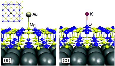 | ||
| Fig. 22 Optimal geometries of (a) a Au atom adsorbed on top of a Mg cation of a MgO/Ag(100) 2 ML film and (b) a K atom adsorbed on top of an O anion of a MgO/Ag(100) 2 ML film. In both cases notice the strong relaxation of the surface ion in direct contact with the adsorbate. The inset shows a top view of the 3 × 3 supercell used in the calculations. Reproduced with permission from ref. 242. Copyright 2006 by the Royal Chemical Society. | ||
4 From model systems to real catalysts
We have seen in the previous sections how thin oxide films may be used to model specific aspects of heterogeneous catalysts by catching some of the complexity of the real powder system. In many cases lessons may be learned by experimentally testing existing hypotheses that have been used to explain observed behavior using specifically designed model systems.4.1 Doping
One example was the specific electron induced reactivity of carbon-dioxide and the formation of oxalate species at the rim of a Au nanoparticle supported on a thin MgO film grown on Ag.40,202 The question is whether there is a way to transfer the knowledge gained to the design of systems closer to the reality of a powder system. In order to see the connection, let us remember that we considered the transfer of charge from the metal substrate, which led to the specific flat morphology of the Au particle and the localization of this charge at the nano-particle's rim. The energetics involve the energy necessary to release electrons from the electron source, i.e. the metal (Ag) support, and the electron affinity of the surface species, i.e. the Au particle. If we can place an electron source within the bulk of an oxide support to mimic the corresponding energetics, a similar situation should be encountered, as anticipated in Section 2.2.2.120,159,206,243–245Fig. 23 shows STM images of a 60 ML thick CaO film in a (100) geometry without a Mo dopant (Fig. 23a) and with a Mo dopant (Fig. 23b).244 Clearly, the doped material leads to an equivalent flat morphology of the Au nano-particle triggered by the electron transfer (see also Fig. 8). If a co-dopant with higher electron affinity is present, then the effect on the Au particle's morphology disappears. Fig. 23c shows the effect when Li is co-doped with Mo.245 This example indicates how a concept developed on model systems may be directly transferred to bulk materials, as they are used in real catalysts. Of course, there are still a number of open questions as to how the dopant interacts with the Au particle on top of the surface. We infer from investigations involving not adsorbed metal nano-particles but rather molecules, such as O2,243 which exhibit a considerable electron affinity, and which do form anionic species on doped CaO films, that electron phonon coupling is involved in the process,161 as discussed in Section 3.3. There is an experimental study on bulk powder material by the Schlögl group, published back to back with our conceptional work,243,246 that hints to the validity of this.
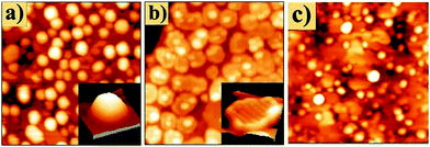 | ||
| Fig. 23 STM images of 0.5 ML Au deposited onto (a) pristine CaO; (b) doped with 4% Mo; (c) doped with 4% Mo + 8% Li (6.0 V, 50 × 50 nm2).244,245 Adapted with permission from ref. 244. Copyright 2012 by the American Physical Society. Adapted with permission from ref. 245. Copyright 2012 American Chemical Society. | ||
4.2 Strong metal support interaction (SMSI)
In the Introduction the so-called Strong Metal Support Interaction (SMSI)25,214,219,247 was mentioned. In a reactive atmosphere a metal particle may be fully or partially encapsulated by a thin oxide layer, which influences the observed chemistry as compared to the pure metal. This has been often observed in real catalysis for reducible oxide supports in particular. TiO2 is the prototypic substrate oxide for which this effect has been extensively observed and discussed.248–251 The structure of the TixOy oxide layer over growing the metal, however, is still under debate.213,220,252–256 Another system has therefore been chosen to attempt a deeper understanding of the way SMSI states of catalysts influence the chemistry. The particular system is Pt (and/or) Pd on magnetite. Fig. 24 shows STM images of Pt particles grown on Fe3O4(111) after treatment at higher temperatures, which led to the growth of an ultrathin FeO layer on top of the particles.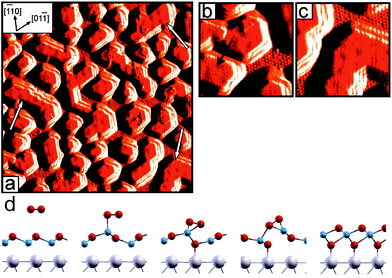 | ||
| Fig. 24 STM topographic images of 3D Pt clusters (covered with a thin FeO layer after thermal treatment), where some of the descending terraces at the cluster rim are resolved. (a) STM image (scan size 80 × 80 nm2, It = 0.6 nA, Vs = −0.5 V) of 1.8 monolayer (ML) Pt/Fe3O4(111) exposed to 540 Langmuir (L) at 500 K and flashed to 850 K in ultra-high vacuum (UHV). The arrows indicate some of the top facets where the Moiré superstructure is clearly observed, as enlarged in image (b). The Pt particle exhibiting a structure of about 0.6 nm periodicity is shown in image (c) (scan size 20 × 20 nm2). From ref. 214 and 257. Reprinted with permission from ref. 214. Copyright 2008 American Chemical Society. (d) Schematic representation of the transformation of an FeO bi-layer into an FeO2 tri-layer on Pt(111) (Fe: blue, O: red, Pt: grey). Adapted with permission from ref. 257. Copyright 2010 Wiley-VCH. | ||
The STM images clearly reveal the structure of the iron oxide layer and allow us to identify it as a double Fe–O-layer, which have been previously studied extensively as grown on Pt(111) metal single crystals.258–260 Another aspect becomes apparent, which is connected with considerations of general importance for the imaging of three-dimensional particles: imaging of the particle's perimeter is difficult, simply because the size of the tip and the geometry of the STM setup are incompatible with the task.40 However, the structure of the films may be clearly deduced from the atomic resolution at the top facet. Since the structure of the FeO layer on the Pt particles is fully compatible with the one observed on Pt(111) single crystals, model studies have been performed on the single crystal system predominantly (although checked with parallel experiments on particles).247 It was shown that the FeO double layer film, schematically shown in Fig. 24, transforms under oxygen rich conditions into a tri-layer film, also shown with a layer sequence of O–Fe–O/Pt as opposed to O–Fe/Pt.261 This tri-layer exhibits considerable activity in CO oxidation at low temperature. The transformations were supported by a series of density functional calculations.26 The structure of the tri-layer is actually not covering the entire surface, but is embedded in the bilayer FeO film.217,262 Originally, the observed reaction was rationalized by assuming that the top oxygen layer of the tri-layer film, which is more weakly bound than the oxygen layer in the double-layer film, leads to the formation of CO2 when exposed to CO, and the oxygen rich conditions are necessary to replenish the oxygen lost in the reaction. The situation becomes more complex, if the double-layer film does not cover the surface completely. Bao et al.263 presented evidence employing UHV studies that in this case the open FeO/Pt interface is the active site for the reaction. Using additional studies,264 including extensive STM investigations, those authors concluded that oxygen atoms, bound both to the FeO layer and to the Pt substrate, react with incoming CO to form CO2. One has to remember that those studies were performed under UHV conditions, while the abovementioned ones under ambient conditions force the formation of the tri-layer, alluded to above. In order to evaluate the influence of the open oxide–Pt interface, studies on partially covered Pt single crystals at near atmospheric pressure were performed.265 Indeed, the results indicated that the Pt–oxide interface is more reactive than the fully covered film.266–271 Therefore, until recently, there has been evidence that the open oxide–metal interface (in the spirit of an inverse catalyst: see Section 3.2) is the active site. Very recently, however, experimental evidence that the most active interface under ambient conditions is not the oxide–metal interface but rather the oxide–oxide interface between the FeO double-layer and the FeO2−x tri-layer has been provided.272Fig. 25 shows STM topographic images of iron oxide islands formed under ambient conditions. The light protrusions on the iron oxide islands represent those areas where the FeO2 tri-layer has been formed. Panel b in Fig. 25 shows the FeO2−x surface area, i.e. its reduction, normalized to the total island area, after exposure to CO for various times. The plot reveals first order kinetics typical for etching of two-dimensional islands from the edges.273
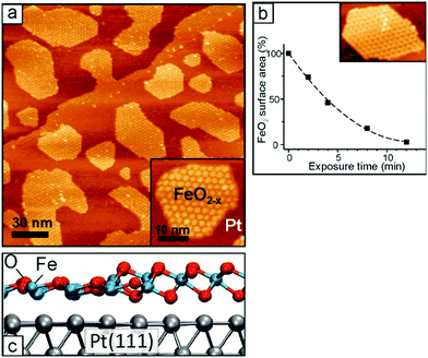 | ||
| Fig. 25 (a) Typical morphology of oxidized FeO2−x films on Pt(111) at sub-monolayer coverages. The cross-view of a FeO2−x/Pt(111) film is shown in the inset. (b) The FeO2−x surface area normalized to the area in the “as prepared” sample as a function of the accumulative exposure time.272 (c) Schematic based on calculations of the FeO/FeO2−x interface after ref. 265. Copyright 2015 Wiley-VCH. | ||
A closer look (Fig. 26) indicates that the FeO2−x protrusions disappear starting from the side that is close to the overall island's rim.
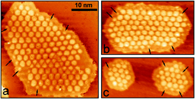 | ||
| Fig. 26 STM images of the FeO2−x islands after exposure to 10−6 mbar CO at 400 K for 4 min. Tunneling conditions: bias −3 V, current 0.05 nA. The arrows highlight non-uniform disappearance of the Moiré spots close to the island edge.272 Reproduced with permission from ref. 272. Copyright 2015 Wiley-VCH. | ||
The reduction thus takes place only at the interface between the “compact” FeO2 domain and the reduced FeO surface formed via reduction. This is a scenario compatible with DFT calculations265 for periodic structures, which revealed the lowest oxygen binding energy at the intrinsic FeO/FeO2−x interface. If the iron oxide islands are exposed to mixtures of CO and oxygen, STM images basically corroborate the previous observation that CO/O2 mixtures with excess CO reduce the islands and excess oxygen prevents excess reduction. However, even oxygen in large (9/1) excess does not prevent the edges (i.e. the metal–oxide interface) from being reduced. In order to link the structural observations to reactivity, a set of experiments using a mass spectrometer placed close to the film surface to measure the amount of CO2 produced were carried out.272 The results obtained for a CO/O2:1/5 mixture in the 10−6 mbar range are shown in Fig. 27.
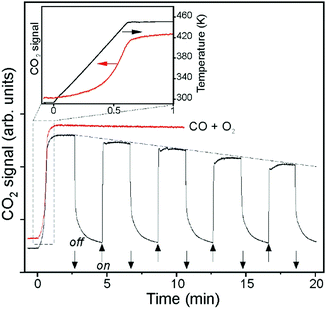 | ||
| Fig. 27 CO2 (44 amu) signal measured by QMS in front of the sub-monolayer FeO2−x film. The reaction (CO/O2 = 1/5) mixture consists of 10−6 mbar of CO and 5 × 10⁻⁶ mbar of O2. At time zero, the sample was heated up to the reaction temperature of 450 K with a rate of 2 K s−1. The red curve shows CO2 production under steady state conditions. The black curve shows CO2 kinetics upon switching O2 flow in the mixture off and on, as indicated by the arrows, while keeping the CO pressure constant.272 Reproduced with permission from ref. 272. Copyright 2015 Wiley-VCH. | ||
At 450 K the reaction ignites and sustained CO2 production (10 minutes) is observed. CO2 formation decreases when the oxygen flow is stopped and recovers when the oxygen is readmitted, but the CO2 production never fully recovers, in fact it decreases as the number of cycles increases. This is consistent with the idea alluded to above that even excess oxygen will not recover the metal/oxide interface but the perimeter length of the interface between the reduced FeO-like region and the FeO2−x region shrinks almost linearly. Therefore, the combination of structural and activity data provides compelling evidence that the FeO/FeO2−x-interface is the most active site. This result has been obtained for flat single crystals but not yet for particles. Nevertheless, given the structural similarities of the ultrathin oxide film on the single crystal and on the particles it is not unlikely that this scenario applies to the SMSI state of Pt/Fe3O4 under reaction conditions.
5 Epilogue
We have reviewed the state of the art in model catalysis both from a theoretical and from an experimental point of view, with particular emphasis on the exchange of charge between the oxide support and the supported metal particle. In many cases the relevant information is gained by combining theory and experiment. For this purpose it is important that both the experimentalist and the theorist try to use tools and develop model systems that can be treated with both approaches. This review covers the discussion of the concepts used, the way the systems may be prepared experimentally and controlled at the atomic level, which is a prerequisite to be able to compare directly to theory. For the latter, atomic control is part of the approach; experimentally it may be challenging sometimes. Still, the best results are obtained if efforts are made on both sides in this direction. In this review we present a number of examples where this goal has been achieved and our understanding of concepts useful for catalysis has been enriched. There are even case studies touched upon which bring model systems in direct contact with real powder catalysis. We believe that the future of more such investigations is bright.Conflicts of interest
There are no conflicts to declare.Acknowledgements
Prof. H. Häkkinen, Dr J. Goniakowski, Prof. C. Noguera, Prof. J. Sauer, and Prof. W.-D. Schneider are thanked for their discussion and collaboration. GF would like to thank his coworkers Dr L. Giordano and Dr S. Tosoni as well as students and post-docs involved in this research activity. His work is presently supported by the Italian MIUR through the PRIN Project 2015K7FZLH SMARTNESS. HJF would like to thank his long-term collaborators Dr M. Heyde, Prof. N. Nilius, Dr Th. Schmidt, Dr S. Shaikhutdinov, and Prof. M. Sterrer, as well as the postdoctoral associates and PhD students involved in the studies presented for their most important contributions. He would also like to thank the German Science Foundation (DFG) for support through the Cluster of Excellence UNICAT (administered by Technical University Berlin) and support through the Collaborative Research Center 1109 (Water/Oxide Interfaces) and for a grant from a DFG-NSFC (No. FR554718-1). Continuous support from the Fonds der Chemischen Industrie is gratefully acknowledged as well. Open Access funding provided by the Max Planck Society.References
- J. Libuda and H.-J. Freund, Surf. Sci. Rep., 2005, 57, 157–298 CrossRef CAS
.
- M. Salmeron and R. Schlögl, Surf. Sci. Rep., 2008, 63, 169–199 CrossRef CAS
.
- G. A. Somorjai and J. Y. Park, Chem. Soc. Rev., 2008, 37, 2155–2162 RSC
.
- A. T. Bell, Science, 2003, 299, 1688–1691 CrossRef CAS PubMed
.
- M. Besson, P. Gallezot and C. Pinel, Chem. Rev., 2014, 114, 1827–1870 CrossRef CAS PubMed
.
-
I. Chorkendorff and J. W. Niemantsverdriet, Concepts of Modern Catalysis and Kinetics, Wiley-VCH, 2017 Search PubMed
.
- B. Roldan Cuenya and F. Behafarid, Surf. Sci. Rep., 2015, 70, 135–187 CrossRef CAS
.
- W. P. Halperin, Rev. Mod. Phys., 1986, 58, 533–606 CrossRef CAS
.
- Y. Lei, F. Mehmood, S. Lee, J. Greeley, B. Lee, S. Seifert, R. E. Winans, J. W. Elam, R. J. Meyer, P. C. Redfern, D. Teschner, R. Schlögl, M. J. Pellin, L. A. Curtiss and S. Vajda, Science, 2010, 328, 224–228 CrossRef CAS PubMed
.
- E. C. Tyo and S. Vajda, Nat. Nanotechnol., 2015, 10, 577 CrossRef CAS PubMed
.
- R. Erni, M. D. Rossell, C. Kisielowski and U. Dahmen, Phys. Rev. Lett., 2009, 102, 096101 CrossRef PubMed
.
- M. A. Bañares, Catal. Today, 2005, 100, 71–77 CrossRef
.
- A. A. Herzing, C. J. Kiely, A. F. Carley, P. Landon and G. J. Hutchings, Science, 2008, 321, 1331–1335 CrossRef CAS PubMed
.
- A. Chakrabarti, M. E. Ford, D. Gregory, R. Hu, C. J. Keturakis, S. Lwin, Y. Tang, Z. Yang, M. Zhu, M. A. Bañares and I. E. Wachs, Catal. Today, 2017, 283, 27–53 CrossRef CAS
.
- S. Tosoni and G. Pacchioni, J. Phys. Chem. C, 2017, 121, 28328–28338 CAS
.
- Y. Romanyshyn, S. Guimond, H. Kuhlenbeck, S. Kaya, R. P. Blum, H. Niehus, S. Shaikhutdinov, M. Simic-Milosevic, N. Nilius, H. J. Freund, M. V. Ganduglia-Pirovano, R. Fortrie, J. Döbler and J. Sauer, Top. Catal., 2008, 50, 106–115 CrossRef CAS
.
- G. Pacchioni, Phys. Chem. Chem. Phys., 2013, 15, 1737–1757 RSC
.
- A. S. K. Hashmi and G. J. Hutchings, Angew. Chem., Int. Ed., 2006, 45, 7896–7936 CrossRef PubMed
.
- M. Haruta, Chem. Rec., 2003, 3, 75–87 CrossRef CAS PubMed
.
- A. S. Wörz, U. Heiz, F. Cinquini and G. Pacchioni, J. Phys. Chem. B, 2005, 109, 18418–18426 CrossRef PubMed
.
- A. M. Márquez, J. Graciani and J. F. Sanz, Theor. Chem. Acc., 2010, 126, 265–273 CrossRef
.
- E. W. McFarland and H. Metiu, Chem. Rev., 2013, 113, 4391–4427 CrossRef CAS PubMed
.
- C. T. Campbell, Nat. Chem., 2012, 4, 597 CrossRef CAS PubMed
.
- S. J. Tauster, S. C. Fung and R. L. Garten, J. Am. Chem. Soc., 1978, 100, 170–175 CrossRef CAS
.
- S. J. Tauster, Acc. Chem. Res., 1987, 20, 389–394 CrossRef CAS
.
- Y. N. Sun, L. Giordano, J. Goniakowski, M. Lewandowski, Z. H. Qin, C. Noguera, S. Shaikhutdinov, G. Pacchioni and H. J. Freund, Angew. Chem., Int. Ed., 2010, 49, 4418–4421 CrossRef CAS PubMed
.
- G. M. Schwab and K. Koller, J. Am. Chem. Soc., 1968, 90, 3078–3080 CrossRef CAS
.
- F. Solymosi, Catal. Rev.: Sci. Eng., 1968, 1, 233–255 Search PubMed
.
- F. F. Vol'kenshtein, Russ. Chem. Rev., 1966, 35, 537 CrossRef
.
- D. W. Goodman, Surf. Sci., 1994, 299–300, 837–848 CrossRef CAS
.
- H. J. Freund, Surf. Sci., 2002, 500, 271–299 CrossRef CAS
.
- C. R. Henry, Surf. Sci. Rep., 1998, 31, 231–326 CrossRef CAS
.
- C. Stampfl, M. Veronica Ganduglia-Pirovano, K. Reuter and M. Scheffler, Surf. Sci., 2002, 500, 368–394 CrossRef CAS
.
- P. S. Bagus, F. Illas, G. Pacchioni and F. Parmigiani, J. Electron Spectrosc. Relat. Phenom., 1999, 100, 215–236 CrossRef CAS
.
- Y. Zhou, J. M. Perket and J. Zhou, J. Phys. Chem. C, 2010, 114, 11853–11860 CAS
.
- P. Torelli, L. Giordano, S. Benedetti, P. Luches, E. Annese, S. Valeri and G. Pacchioni, J. Phys. Chem. C, 2009, 113, 19957–19965 CAS
.
- N. Nilius, M. V. Ganduglia-Pirovano, V. Brázdová, M. Kulawik, J. Sauer and H. J. Freund, Phys. Rev. Lett., 2008, 100, 096802 CrossRef CAS PubMed
.
- X. Lin, N. Nilius, H. J. Freund, M. Walter, P. Frondelius, K. Honkala and H. Häkkinen, Phys. Rev. Lett., 2009, 102, 206801 CrossRef CAS PubMed
.
- X. Lin, N. Nilius, M. Sterrer, P. Koskinen, H. Häkkinen and H.-J. Freund, Phys. Rev. B: Condens. Matter Mater. Phys., 2010, 81, 153406 CrossRef
.
- W.-D. Schneider, M. Heyde and H.-J. Freund, Chem. – Eur. J., 2018, 24, 2317–2327 CrossRef CAS PubMed
.
- G. N. Vayssilov, Y. Lykhach, A. Migani, T. Staudt, G. P. Petrova, N. Tsud, T. Skála, A. Bruix, F. Illas, K. C. Prince, V. r. Matolín, K. M. Neyman and J. Libuda, Nat. Mater., 2011, 10, 310–315 CrossRef CAS PubMed
.
- Y. Lykhach, S. M. Kozlov, T. Skala, A. Tovt, V. Stetsovych, N. Tsud, F. Dvorak, V. Johanek, A. Neitzel, J. Myslivecek, S. Fabris, V. Matolin, K. M. Neyman and J. Libuda, Nat. Mater., 2016, 15, 284–288 CrossRef CAS PubMed
.
- D. Kong, G. Wang, Y. Pan, S. Hu, J. Hou, H. Pan, C. T. Campbell and J. Zhu, J. Phys. Chem. C, 2011, 115, 6715–6725 CAS
.
- P. Luches, F. Pagliuca, S. Valeri, F. Illas, G. Preda and G. Pacchioni, J. Phys. Chem. C, 2012, 116, 1122–1132 CAS
.
-
V. E. Henrich and P. A. Cox, The Surface Science of Metal Oxides, Cambridge University Press, Cambridge, 1994 Search PubMed
.
-
P. A. Cox, Transition Metal Oxides. An Introduction to their Electronic Structure and Properties, Clarendon, Oxford, 1992 Search PubMed
.
- C. T. Campbell, Surf. Sci. Rep., 1997, 27, 1–111 CrossRef CAS
.
- J. Sauer, P. Ugliengo, E. Garrone and V. R. Saunders, Chem. Rev., 1994, 94, 2095–2160 CrossRef CAS
.
- G. Pacchioni, J. M. Ricart and F. Illas, J. Am. Chem. Soc., 1994, 116, 10152–10158 CrossRef CAS
.
- A. L. Shluger, P. V. Sushko and L. N. Kantorovich, Phys. Rev. B: Condens. Matter Mater. Phys., 1999, 59, 2417–2430 CrossRef CAS
.
- M. Chiesa, E. Giamello, C. Di Valentin, G. Pacchioni, Z. Sojka and S. Van Doorslaer, J. Am. Chem. Soc., 2005, 127, 16935–16944 CrossRef CAS PubMed
.
- J. C. Lian, E. Finazzi, C. Di Valentin, T. Risse, H. J. Gao, G. Pacchioni and H. J. Freund, Chem. Phys. Lett., 2008, 450, 308–311 CrossRef CAS
.
- E. Finazzi, C. Di Valentin, G. Pacchioni, M. Chiesa, E. Giamello, H. Gao, J. Lian, T. Risse and H.-J. Freund, Chem. – Eur. J., 2008, 14, 4404–4414 CrossRef CAS PubMed
.
- A. Ruiz Puigdollers, S. Tosoni and G. Pacchioni, J. Phys. Chem. C, 2016, 120, 15329–15337 CAS
.
- A. R. Puigdollers, F. Illas and G. Pacchioni, J. Phys. Chem. C, 2016, 120, 4392–4402 CAS
.
- M. Antlanger, W. Mayr-Schmölzer, J. Pavelec, F. Mittendorfer, J. Redinger, P. Varga, U. Diebold and M. Schmid, Phys. Rev. B: Condens. Matter Mater. Phys., 2012, 86, 035451 CrossRef
.
- H. Li, J.-I. J. Choi, W. Mayr-Schmölzer, C. Weilach, C. Rameshan, F. Mittendorfer, J. Redinger, M. Schmid and G. Rupprechter, J. Phys. Chem. C, 2015, 119, 2462–2470 CAS
.
- E. Napetschnig, M. Schmid and P. Varga, Surf. Sci., 2008, 602, 1750–1756 CrossRef CAS
.
- V. Maurice, M. Salmeron and G. A. Somorjai, Surf. Sci., 1990, 237, 116–126 CrossRef CAS
.
- K. Meinel, A. Eichler, S. Förster, K. M. Schindler, H. Neddermeyer and W. Widdra, Phys. Rev. B: Condens. Matter Mater. Phys., 2006, 74, 235444 CrossRef
.
- K. Meinel, A. Eichler, K. M. Schindler and H. Neddermeyer, Surf. Sci., 2004, 562, 204–218 CrossRef CAS
.
- K. Meinel, K.-M. Schindler and H. Neddermeyer, Surf. Sci., 2003, 532-535, 420–424 CrossRef CAS
.
- A. Ruiz Puigdollers and G. Pacchioni, Nanoscale, 2017, 9, 6866–6876 RSC
.
- J. F. Sanz and A. Márquez, J. Phys. Chem. C, 2007, 111, 3949–3955 CAS
.
- Y. Han, C.-j. Liu and Q. Ge, J. Phys. Chem. B, 2006, 110, 7463–7472 CrossRef CAS PubMed
.
- T. Bredow, E. Aprà, M. Catti and G. Pacchioni, Surf. Sci., 1998, 418, 150–165 CrossRef CAS
.
- M. A. San Miguel, C. J. Calzado and J. F. Sanz, J. Phys. Chem. B, 2001, 105, 1794–1798 CrossRef CAS
.
- T. Albaret, F. Finocchi, C. Noguera and A. De Vita, Phys. Rev. B: Condens. Matter Mater. Phys., 2001, 65, 035402 CrossRef
.
- M. Sterrer, M. Yulikov, T. Risse, H.-J. Freund, J. Carrasco, F. Illas, C. Di Valentin, L. Giordano and G. Pacchioni, Angew. Chem., Int. Ed., 2006, 45, 2633–2635 CrossRef CAS PubMed
.
- C. D. Wagner, Anal. Chem., 1972, 44, 967–973 CrossRef CAS
.
- C. D. Wagner, L. H. Gale and R. H. Raymond, Anal. Chem., 1979, 51, 466–482 CrossRef CAS
.
- A. Bruix, K. M. Neyman and F. Illas, J. Phys. Chem. C, 2010, 114, 14202–14207 CAS
.
- G. Vilé, B. Bridier, J. Wichert and J. Pérez-Ramírez, Angew. Chem., Int. Ed., 2012, 51, 8620–8623 CrossRef PubMed
.
- G. Vilé, S. Wrabetz, L. Floryan, M. E. Schuster, F. Girgsdies, D. Teschner and J. Pérez-Ramírez, ChemCatChem, 2014, 6, 1928–1934 CrossRef
.
- K. Werner, X. Weng, F. Calaza, M. Sterrer, T. Kropp, J. Paier, J. Sauer, M. Wilde, K. Fukutani, S. Shaikhutdinov and H.-J. Freund, J. Am. Chem. Soc., 2017, 139, 17608–17616 CrossRef CAS PubMed
.
- M. Wilde and K. Fukutani, Surf. Sci. Rep., 2014, 69, 196–295 CrossRef CAS
.
- H. L. Tuller and S. R. Bishop, Annu. Rev. Mater. Res., 2011, 41, 369–398 CrossRef CAS
.
- P. Baranek, G. Pinarello, C. Pisani and R. Dovesi, Phys. Chem. Chem. Phys., 2000, 2, 3893–3901 RSC
.
- A. M. Ferrari and G. Pacchioni, J. Phys. Chem., 1995, 99, 17010–17018 CrossRef CAS
.
- J. Kramer, W. Ernst, C. Tegenkamp and H. Pfnür, Surf. Sci., 2002, 517, 87–97 CrossRef CAS
.
- L. N. Kantorovich, J. M. Holender and M. J. Gillan, Surf. Sci., 1995, 343, 221–239 CrossRef CAS
.
- E. Scorza, U. Birkenheuer and C. Pisani, J. Chem. Phys., 1997, 107, 9645–9658 CrossRef CAS
.
- L. Ojamäe and C. Pisani, J. Chem. Phys., 1998, 109, 10984–10995 CrossRef
.
- O. Diwald, M. Sterrer and E. Knozinger, Phys. Chem. Chem. Phys., 2002, 4, 2811–2817 RSC
.
- M. Ulmann, N. R. De Tacconi and J. Augustynski, J. Phys. Chem., 1986, 90, 6523–6530 CrossRef CAS
.
- D. Chen, C. Chen, Z. M. Baiyee, Z. Shao and F. Ciucci, Chem. Rev., 2015, 115, 9869–9921 CrossRef CAS PubMed
.
- M. Chiesa, F. Napoli and E. Giamello, J. Phys. Chem. C, 2007, 111, 5481–5485 CAS
.
- F. Napoli, M. Chiesa, E. Giamello, E. Finazzi, C. Di Valentin and G. Pacchioni, J. Am. Chem. Soc., 2007, 129, 10575–10581 CrossRef CAS PubMed
.
- S. A. Chambers, T. Droubay, D. R. Jennison and T. R. Mattsson, Science, 2002, 297, 827–831 CrossRef CAS PubMed
.
- D. Ricci, C. Di Valentin, G. Pacchioni, P. V. Sushko, A. L. Shluger and E. Giamello, J. Am. Chem. Soc., 2003, 125, 738–747 CrossRef CAS PubMed
.
- M. Chiesa, M. C. Paganini, E. Giamello, C. Di Valentin and G. Pacchioni, Angew. Chem., Int. Ed., 2003, 42, 1759–1761 CrossRef CAS PubMed
.
- M. Chiesa, M. C. Paganini, E. Giamello, D. M. Murphy, C. Di Valentin and G. Pacchioni, Acc. Chem. Res., 2006, 39, 861–867 CrossRef CAS PubMed
.
- F. Napoli, M. Chiesa, E. Giamello, E. Finazzi, C. Di Valentin and G. Pacchioni, J. Am. Chem. Soc., 2007, 129, 10575–10581 CrossRef CAS PubMed
.
- K. P. McKenna and A. Shluger, Nat. Mater., 2008, 7, 859–862 CrossRef CAS PubMed
.
- X. Lin, B. Yang, H. M. Benia, P. Myrach, M. Yulikov, A. Aumer, M. Brown, M. Sterrer, O. Bondarchuk, E. Kieseritzky, J. Rocker, T. Risse, H. Gao, N. Nilius and H. J. Freund, J. Am. Chem. Soc., 2010, 132, 7745–7749 CrossRef CAS PubMed
.
- G. Pacchioni, ChemPhysChem, 2003, 4, 1041–1047 CrossRef CAS PubMed
.
- G. Stapper, M. Bernasconi, N. Nicoloso and M. Parrinello, Phys. Rev. B: Condens. Matter Mater. Phys., 1999, 59, 797–810 CrossRef CAS
.
- G. Pacchioni and G. Ieranò, Phys. Rev. Lett., 1997, 79, 753–756 CrossRef CAS
.
- C. Di Valentin, G. Pacchioni and A. Selloni, Phys. Rev. Lett., 2006, 97, 166803 CrossRef PubMed
.
- A. Migani, G. N. Vayssilov, S. T. Bromley, F. Illas and K. M. Neyman, J. Mater. Chem., 2010, 20, 10535–10546 RSC
.
- J.-F. Jerratsch, X. Shao, N. Nilius, H.-J. Freund, C. Popa, M. V. Ganduglia-Pirovano, A. M. Burow and J. Sauer, Phys. Rev. Lett., 2011, 106, 246801 CrossRef PubMed
.
- L. Giordano, C. Di Valentin, J. Goniakowski and G. Pacchioni, Phys. Rev. Lett., 2004, 92, 096105 CrossRef PubMed
.
- A. Bogicevic and D. R. Jennison, Surf. Sci., 2002, 515, L481–L486 CrossRef CAS
.
- T. König, G. H. Simon, U. Martinez, L. Giordano, G. Pacchioni, M. Heyde and H.-J. Freund, ACS Nano, 2010, 4, 2510–2514 CrossRef PubMed
.
- A. Del Vitto, L. Giordano, G. Pacchioni and N. Rösch, Surf. Sci., 2005, 575, 103–114 CrossRef CAS
.
- M. Sterrer, M. Yulikov, E. Fischbach, M. Heyde, H.-P. Rust, G. Pacchioni, T. Risse and H.-J. Freund, Angew. Chem., Int. Ed., 2006, 45, 2630–2632 CrossRef CAS PubMed
.
- S. Fabris, G. Vicario, G. Balducci, S. de Gironcoli and S. Baroni, J. Phys. Chem. B, 2005, 109, 22860–22867 CrossRef CAS PubMed
.
- E. Wuilloud, B. Delley, W. D. Schneider and Y. Baer, Phys. Rev. Lett., 1984, 53, 202–205 CrossRef CAS
.
- N. A. Deskins and M. Dupuis, Phys. Rev. B: Condens. Matter Mater. Phys., 2007, 75, 195212 CrossRef
.
- I. Bannat, K. Wessels, T. Oekermann, J. Rathousky, D. Bahnemann and M. Wark, Chem. Mater., 2009, 21, 1645–1653 CrossRef CAS
.
- X.-Q. Gong, A. Selloni, O. Dulub, P. Jacobson and U. Diebold, J. Am. Chem. Soc., 2008, 130, 370–381 CrossRef CAS PubMed
.
- Z. Hu, B. Li, X. Sun and H. Metiu, J. Phys. Chem. C, 2011, 115, 3065–3074 CAS
.
- V. Shapovalov and H. Metiu, J. Catal., 2007, 245, 205–214 CrossRef CAS
.
- N. Mammen, S. Narasimhan and S. d. Gironcoli, J. Am. Chem. Soc., 2011, 133, 2801–2803 CrossRef CAS PubMed
.
- X. Shao, S. Prada, L. Giordano, G. Pacchioni, N. Nilius and H.-J. Freund, Angew. Chem., Int. Ed., 2011, 50, 11525–11527 CrossRef CAS PubMed
.
- M. Bäumer and H.-J. Freund, Prog. Surf. Sci., 1999, 61, 127–198 CrossRef
.
- X. Lai, T. P. S. Clair, M. Valden and D. W. Goodman, Prog. Surf. Sci., 1998, 59, 25–52 CrossRef CAS
.
- D. Ricci, A. Bongiorno, G. Pacchioni and U. Landman, Phys. Rev. Lett., 2006, 97, 036106 CrossRef PubMed
.
- M. Sterrer, T. Risse, M. Heyde, H.-P. Rust and H.-J. Freund, Phys. Rev. Lett., 2007, 98, 206103 CrossRef PubMed
.
- F. Stavale, X. Shao, N. Nilius, H.-J. Freund, S. Prada, L. Giordano and G. Pacchioni, J. Am. Chem. Soc., 2012, 134, 11380–11383 CrossRef CAS PubMed
.
- M. Xu, T. Liang, M. Shi and H. Chen, Chem. Rev., 2013, 113, 3766–3798 CrossRef CAS PubMed
.
- M. Osada and T. Sasaki, Adv. Mater., 2012, 24, 210–228 CrossRef CAS PubMed
.
- G. Pacchioni, Chem. – Eur. J., 2012, 18, 10144–10158 CrossRef CAS PubMed
.
-
E. P. Gusev, in Defects in SiO2 and Related Dielectrics: Science and Technology, ed. G. Pacchioni, L. Skuja and D. L. Griscom, Springer Netherlands, Dordrecht, 2000, pp. 557–579 DOI:10.1007/978-94-010-0944-7_21
.
- C. O. A. Olsson and D. Landolt, Electrochim. Acta, 2003, 48, 1093–1104 CrossRef CAS
.
- D. Costa, T. Ribeiro, F. Mercuri, G. Pacchioni and P. Marcus, Adv. Mater. Interfaces, 2014, 1, 1300072 CrossRef
.
- C. H. Ahn, K. M. Rabe and J.-M. Triscone, Science, 2004, 303, 488–491 CrossRef CAS PubMed
.
- C. G. Granqvist, Sol. Energy Mater. Sol. Cells, 2007, 91, 1529–1598 CrossRef CAS
.
- S. S. P. Parkin, C. Kaiser, A. Panchula, P. M. Rice, B. Hughes, M. Samant and S.-H. Yang, Nat. Mater., 2004, 3, 862–867 CrossRef CAS PubMed
.
-
Oxide Ultrathin Films: Science and Technology, ed. G. Pacchioni and S. Valeri, Wiley-VCH, Weinheim, 2012 Search PubMed
.
- X. Xu and D. W. Goodman, Appl. Phys. Lett., 1992, 61, 774–776 CrossRef CAS
.
- H. J. Freund, H. Kuhlenbeck and V. Staemmler, Rep. Prog. Phys., 1996, 59, 283–347 CrossRef CAS
.
- H.-J. Freund and G. Pacchioni, Chem. Soc. Rev., 2008, 37, 2224–2242 RSC
.
- S. Surnev, M. G. Ramsey and F. P. Netzer, Prog. Surf. Sci., 2003, 73, 117–165 CrossRef CAS
.
- Q.-H. Wu, A. Fortunelli and G. Granozzi, Int. Rev. Phys. Chem., 2009, 28, 517–576 CrossRef CAS
.
- L. Giordano and G. Pacchioni, Acc. Chem. Res., 2011, 44, 1244–1252 CrossRef CAS PubMed
.
- G. Pacchioni and H.-J. Freund, Chem. Rev., 2013, 113, 4035–4072 CrossRef CAS PubMed
.
- M. Frank, M. Bäumer, R. Kühnemuth and H.-J. Freund, J. Phys. Chem. B, 2001, 105, 8569–8576 CrossRef CAS
.
-
S. C. Street and D. W. Goodman, in Growth and Properties of Ultrathin Epitaxial Layers, The Chemical Physics of Solid Surfaces, ed. D. A. King and D. P. Woodruff, Elsevier, New York, 1997, vol. 8, p. 375 Search PubMed
.
- U. Heiz, F. Vanolli, L. Trento and W. D. Schneider, Rev. Sci. Instrum., 1997, 68, 1986 CrossRef CAS
.
- M. C. Wu, J. S. Corneille, C. A. Estrada, J.-W. He and D. W. Goodman, Chem. Phys. Lett., 1991, 182, 472–478 CrossRef CAS
.
- M. C. Wu, J. S. Corneille, J. W. He, C. A. Estrada and D. W. Goodman, J. Vac. Sci. Technol., A, 1992, 10, 1467–1471 CAS
.
- X. Shao, P. Myrach, N. Nilius and H.-J. Freund, J. Phys. Chem. C, 2011, 115, 8784 CAS
.
- M. Liehr, P. A. Thiry, J. J. Pireaux and R. Caudano, Phys. Rev. B: Condens. Matter Mater. Phys., 1986, 33, 5682–5697 CrossRef CAS
.
- L. H. Tjeng, A. R. Vos and G. A. Sawatzky, Surf. Sci., 1990, 235, 269–279 CrossRef CAS
.
- J.-W. He and P. J. Møller, Surf. Sci., 1986, 178, 934–942 CrossRef CAS
.
- J.-W. He and P. J. Møller, Surf. Sci., 1987, 180, 411–420 CrossRef CAS
.
- I. Alstrup and P. J. Møller, Appl. Surf. Sci., 1988, 33–34, 143–151 CrossRef
.
- S. Schintke, S. Messerli, M. Pivetta, F. Patthey, L. Libioulle, M. Stengel, A. De Vita and W.-D. Schneider, Phys. Rev. Lett., 2001, 87, 2768011 CrossRef PubMed
.
- J. Pal, M. Smerieri, E. Celasco, L. Savio, L. Vattuone and M. Rocca, Phys. Rev. Lett., 2014, 112, 126102 CrossRef PubMed
.
- R. G. S. Pala and H. Metiu, J. Phys. Chem. C, 2007, 111, 12715–12722 CAS
.
- S. Baumann, I. G. Rau, S. Loth, C. P. Lutz and A. J. Heinrich, ACS Nano, 2014, 8, 1739–1744 CrossRef CAS PubMed
.
- K. P. McKenna and A. L. Shluger, Phys. Rev. B: Condens. Matter Mater. Phys., 2009, 79, 224116 CrossRef
.
- H. M. Benia, P. Myrach, A. Gonchar, T. Risse, M. Nilius and H. J. Freund, Phys. Rev. B: Condens. Matter Mater. Phys., 2010, 81, 241415 CrossRef
.
- S. Stuckenholz, C. Büchner, M. Heyde and H.-J. Freund, J. Phys. Chem. C, 2015, 119, 12283–12290 CAS
.
- T. König, G. H. Simon, H. P. Rust, G. Pacchioni, M. Heyde and H. J. Freund, J. Am. Chem. Soc., 2009, 131, 17544–17545 CrossRef PubMed
.
- M. Heyde, G. H. Simon, H.-P. Rust and H.-J. Freund, Appl. Phys. Lett., 2006, 89, 263107 CrossRef
.
- S. Schintke and W. D. Schneider, J. Phys.: Condens. Matter, 2004, 16, R49 CrossRef CAS
.
- Y. Cui, X. Shao, S. Prada, L. Giordano, G. Pacchioni, H.-J. Freund and N. Nilius, Phys. Chem. Chem. Phys., 2014, 16, 12764–12772 RSC
.
- Y. Cui, Y. Pan, L. Pascua, H. Qiu, C. Stiehler, H. Kuhlenbeck, N. Nilius and H.-J. Freund, Phys. Rev. B: Condens. Matter Mater. Phys., 2015, 91, 035418 CrossRef
.
- Y. Cui, S. Tosoni, W.-D. Schneider, G. Pacchioni, N. Nilius and H.-J. Freund, Phys. Rev. Lett., 2015, 114, 016804 CrossRef PubMed
.
- H.-J. Freund, Acc. Chem. Res., 2017, 50, 446–449 CrossRef CAS PubMed
.
- C. Büchner, L. Lichtenstein, X. Yu, J. A. Boscoboinik, B. Yang, W. E. Kaden, M. Heyde, S. K. Shaikhutdinov, R. Włodarczyk, M. Sierka, J. Sauer and H.-J. Freund, Chem. – Eur. J., 2014, 20, 9176–9183 CrossRef PubMed
.
- X. Yu, B. Yang, J. A. Boscoboinik, S. Shaikhutdinov and H.-J. Freund, Appl. Phys. Lett., 2012, 100, 151608 CrossRef
.
- M. Heyde, S. Shaikhutdinov and H.-J. Freund, Chem. Phys. Lett., 2012, 550, 1–7 CrossRef CAS
.
- L. Lichtenstein, M. Heyde and H.-J. Freund, J. Phys. Chem. C, 2012, 116, 20426–20432 CAS
.
- L. Lichtenstein, C. Büchner, B. Yang, S. Shaikhutdinov, M. Heyde, M. Sierka, R. Włodarczyk, J. Sauer and H.-J. Freund, Angew. Chem., Int. Ed., 2012, 51, 404–407 CrossRef CAS PubMed
.
- W. H. Zachariasen, J. Am. Chem. Soc., 1932, 54, 3841–3851 CrossRef CAS
.
- J. P. Hogan, J. Polym. Sci., Part A: Polym. Chem., 1970, 8, 2637–2652 CrossRef CAS
.
- E. Groppo, C. Lamberti, S. Bordiga, G. Spoto and A. Zecchina, Chem. Rev., 2005, 105, 115–184 CrossRef CAS PubMed
.
- B. M. Weckhuysen, R. A. Schoonheydt, J. M. Jehng, I. E. Wachs, S. J. Cho, R. Ryoo, S. Kijlstra and E. Poels, J. Chem. Soc., Faraday Trans., 1995, 91, 3245–3253 RSC
.
-
M. P. McDaniel, in Advances in Catalysis, ed. C. G. Bruce and K. Helmut, Academic Press, 2010, vol. 53, pp. 123–606 Search PubMed
.
- C. Brown, J. Krzystek, R. Achey, A. Lita, R. Fu, R. W. Meulenberg, M. Polinski, N. Peek, Y. Wang, L. J. van de Burgt, S. Profeta, A. E. Stiegman and S. L. Scott, ACS Catal., 2015, 5, 5574–5583 CrossRef CAS
.
- E. Groppo, C. Lamberti, S. Bordiga, G. Spoto and A. Zecchina, J. Catal., 2006, 240, 172–181 CrossRef CAS
.
- E. L. Lee and I. E. Wachs, J. Phys. Chem. C, 2007, 111, 14410–14425 CAS
.
- M. P. Conley, M. F. Delley, G. Siddiqi, G. Lapadula, S. Norsic, V. Monteil, O. V. Safonova and C. Copéret, Angew. Chem., Int. Ed., 2014, 53, 1872–1876 CrossRef PubMed
.
- M. F. Delley, F. Núñez-Zarur, M. P. Conley, A. Comas-Vives, G. Siddiqi, S. Norsic, V. Monteil, O. V. Safonova and C. Copéret, Proc. Natl. Acad. Sci. U. S. A., 2014, 111, 11624–11629 CrossRef CAS PubMed
.
- P. C. Thüne, J. Loos, A. M. de Jong, P. J. Lemstra and J. W. Niemantsverdriet, Top. Catal., 2000, 13, 67–74 CrossRef
.
- P. C. Thüne, J. Loos, X. Chen, E. M. E. van Kimmenade, B. Kong and J. W. Niemantsverdriet, Top. Catal., 2007, 46, 239–245 CrossRef
.
- Q. Pan, L. Li, S. Shaikhutdinov and H.-J. Freund, J. Catal., 2018, 357, 12–19 CrossRef
.
- Q. Pan, L. Li, S. Shaikhutdinov, Y. Fujimori, M. Hollerer, M. Sterrer and H.-J. Freund, Faraday Discuss., 2017 10.1039/C7FD00209B
.
- X. Yu, E. Emmez, Q. Pan, B. Yang, S. Pomp, W. E. Kaden, M. Sterrer, S. Shaikhutdinov, H.-J. Freund, I. Goikoetxea, R. Wlodarczyk and J. Sauer, Phys. Chem. Chem. Phys., 2016, 18, 3755–3764 RSC
.
- B. Yang, E. Emmez, W. E. Kaden, X. Yu, J. A. Boscoboinik, M. Sterrer, S. Shaikhutdinov and H. J. Freund, J. Phys. Chem. C, 2013, 117, 8336–8344 CAS
.
- M. Sterrer and H.-J. Freund, Catal. Lett., 2013, 143, 375–385 CrossRef CAS
.
- J. Libuda, M. Frank, A. Sandell, S. Andersson, P. A. Brühwiler, M. Bäumer, N. Mårtensson and H. J. Freund, Surf. Sci., 1997, 384, 106–119 CrossRef CAS
.
- M. Frank, M. Bäumer, R. Kuehnemuth and H. J. Freund, J. Phys. Chem. B, 2001, 105, 8569 CrossRef CAS
.
- U. Heiz and W. D. Schneider, Crit. Rev. Solid State Mater. Sci., 2001, 26, 251–290 CrossRef CAS
.
- P. Fayet, F. Granzer, G. Hegenbart, E. Moisar, B. Pischel and L. Wöste, Phys. Rev. Lett., 1985, 55, 3002–3004 CrossRef CAS PubMed
.
- N. Nilius, T. M. Wallis and W. Ho, Phys. Rev. Lett., 2003, 90, 046808 CrossRef CAS PubMed
.
- A. Bogicevic and D. R. Jennison, Phys. Rev. Lett., 1999, 82, 4050 CrossRef CAS
.
- K. M. Neyman, S. Vent, N. Rösch and G. Pacchioni, Top. Catal., 1999, 9, 153–161 CrossRef CAS
.
- J. Repp, G. Meyer, F. E. Olsson and M. Persson, Science, 2004, 305, 493–495 CrossRef CAS PubMed
.
- F. E. Olsson, S. Paavilainen, M. Persson, J. Repp and G. Meyer, Phys. Rev. Lett., 2007, 98, 176803 CrossRef
.
- G. Pacchioni, L. Giordano and M. Baistrocchi, Phys. Rev. Lett., 2005, 94, 226104 CrossRef PubMed
.
- M. Sterrer, T. Risse, U. Martinez Pozzoni, L. Giordano, M. Heyde, H.-P. Rust, G. Pacchioni and H.-J. Freund, Phys. Rev. Lett., 2007, 98, 096107 CrossRef PubMed
.
- C. D. Wagner, Faraday Discuss. Chem. Soc., 1975, 60, 291–300 RSC
.
- P. S. Bagus, A. Wieckowski and H. Freund, Chem. Phys. Lett., 2006, 420, 42–46 CrossRef CAS
.
- R. N. Sodhi and R. G. Cavell, J. Electron Spectrosc. Relat. Phenom., 1983, 32, 283–312 CrossRef CAS
.
- G. Hohlneicher, H. Pulm and H.-J. Freund, J. Electron Spectrosc. Relat. Phenom., 1985, 37, 209–224 CrossRef CAS
.
- W. E. Kaden, C. Büchner, L. Lichtenstein, S. Stuckenholz, F. Ringleb, M. Heyde, M. Sterrer, H.-J. Freund, L. Giordano, G. Pacchioni, C. J. Nelin and P. S. Bagus, Phys. Rev. B: Condens. Matter Mater. Phys., 2014, 89, 115436 CrossRef
.
- C. P. O'Brien, K. H. Dostert, M. Hollerer, C. Stiehler, F. Calaza, S. Schauermann, S. Shaikhutdinov, M. Sterrer and H. J. Freund, Faraday Discuss., 2016, 188, 309–321 RSC
.
- F. Calaza, C. Stiehler, Y. Fujimori, M. Sterrer, S. Beeg, M. Ruiz-Oses, N. Nilius, M. Heyde, T. Parviainen, K. Honkala, H. Häkkinen and H.-J. Freund, Angew. Chem., Int. Ed., 2015, 54, 12484–12487 CrossRef CAS PubMed
.
- A. Stamatovic, K. Stephan and T. D. Märk, Int. J. Mass Spectrom. Ion Processes, 1985, 63, 37–47 CrossRef CAS
.
- R. N. Compton, P. W. Reinhardt and C. D. Cooper, J. Chem. Phys., 1975, 63, 3821–3827 CrossRef CAS
.
-
F. M. Hoffmann, M. D. Weisel and J. A. K. Paul, Carbon Dioxide Chemistry, Woodhead Publishing, 1994, pp. 55–63 DOI:10.1016/B978-1-85573-799-0.50011-X
.
- Y. Cui, C. Stiehler, N. Nilius and H.-J. Freund, Phys. Rev. B: Condens. Matter Mater. Phys., 2015, 92, 075444 CrossRef
.
- X. Shao, Y. Cui, W.-D. Schneider, N. Nilius and H.-J. Freund, J. Phys. Chem. C, 2012, 116, 17980–17984 CAS
.
- H.-J. Freund, J. Am. Chem. Soc., 2016, 138, 8985–8996 CrossRef CAS PubMed
.
- Y. Martynova, B. H. Liu, M. E. McBriarty, I. M. N. Groot, M. J. Bedzyk, S. Shaikhutdinov and H. J. Freund, J. Catal., 2013, 301, 227–232 CrossRef CAS
.
- I. X. Green, W. J. Tang, M. Neurock and J. T. Yates, Science, 2011, 333, 736–739 CrossRef CAS PubMed
.
- J. A. Rodriguez, S. Ma, P. Liu, J. Hrbek, J. Evans and M. Pérez, Science, 2007, 318, 1757–1760 CrossRef CAS PubMed
.
- K. Hayek, M. Fuchs, B. Klötzer, W. Reichl and G. Rupprechter, Top. Catal., 2000, 13, 55–66 CrossRef CAS
.
- M. Bowker, P. Stone, P. Morrall, R. Smith, R. Bennett, N. Perkins, R. Kvon, C. Pang, E. Fourre and M. Hall, J. Catal., 2005, 234, 172–181 CrossRef CAS
.
- Z. H. Qin, M. Lewandowski, Y. N. Sun, S. Shaikhutdinov and H. J. Freund, J. Phys. Chem. C, 2008, 112, 10209–10213 CAS
.
- Y.-N. Sun, Z.-H. Qin, M. Lewandowski, S. Kaya, S. Shaikhutdinov and H.-J. Freund, Catal. Lett., 2008, 126, 31–35 CrossRef CAS
.
- Y. Lei, M. Lewandowski, Y.-N. Sun, Y. Fujimori, Y. Martynova, I. M. N. Groot, R. J. Meyer, L. Giordano, G. Pacchioni, J. Goniakowski, C. Noguera, S. Shaikhutdinov and H.-J. Freund, ChemCatChem, 2011, 3, 671–674 CrossRef CAS
.
- L. Giordano, M. Lewandowski, I. M. N. Groot, Y. N. Sun, J. Goniakowski, C. Noguera, S. Shaikhutdinov, G. Pacchioni and H. J. Freund, J. Phys. Chem. C, 2010, 114, 21504–21509 CAS
.
- M. Lewandowski, Y. N. Sun, Z. H. Qin, S. Shaikhutdinov and H. J. Freund, Appl. Catal., A, 2011, 391, 407–410 CrossRef CAS
.
- M. G. Willinger, W. Zhang, O. Bondarchuk, S. Shaikhutdinov, H.-J. Freund and R. Schlögl, Angew. Chem., Int. Ed., 2014, 53, 5998–6001 CrossRef CAS PubMed
.
- O. Dulub, W. Hebenstreit and U. Diebold, Phys. Rev. Lett., 2000, 84, 3646–3649 CrossRef CAS PubMed
.
- S. Helveg, J. V. Lauritsen, E. Lægsgaard, I. Stensgaard, J. K. Nørskov, B. S. Clausen, H. Topsøe and F. Besenbacher, Phys. Rev. Lett., 2000, 84, 951–954 CrossRef CAS PubMed
.
- M. V. Bollinger, J. V. Lauritsen, K. W. Jacobsen, J. K. Nørskov, S. Helveg and F. Besenbacher, Phys. Rev. Lett., 2001, 87, 196803 CrossRef CAS PubMed
.
- L. Giordano, M. Baistrocchi and G. Pacchioni, Phys. Rev. B: Condens. Matter Mater. Phys., 2005, 72, 115403 CrossRef
.
- A. Hellman, S. Klacar and H. Grönbeck, J. Am. Chem. Soc., 2009, 131, 16636–16637 CrossRef CAS PubMed
.
- A. Gonchar, T. Risse, H.-J. Freund, L. Giordano, C. Di Valentin and G. Pacchioni, Angew. Chem., Int. Ed., 2011, 50, 2635–2638 CrossRef CAS PubMed
.
- G. Pacchioni, A. M. Ferrari and E. Giamello, Chem. Phys. Lett., 1996, 255, 58–64 CrossRef CAS
.
- M. Chiesa, E. Giamello, M. C. Paganini, Z. Sojka and D. M. Murphy, J. Chem. Phys., 2002, 116, 4266–4274 CrossRef CAS
.
- F. Napoli, M. Chiesa, E. Giamello, G. Preda, C. Di Valentin and G. Pacchioni, Chem. – Eur. J., 2010, 16, 6776–6785 CrossRef CAS PubMed
.
- C. J. Nelin, P. S. Bagus, M. A. Brown, M. Sterrer and H.-J. Freund, Angew. Chem., Int. Ed., 2011, 50, 10174–10177 CrossRef CAS PubMed
.
- J. Weissenrieder, S. Kaya, J.-L. Lu, H.-J. Gao, S. Shaikhutdinov, H.-J. Freund, M. Sierka, T. K. Todorova and J. Sauer, Phys. Rev. Lett., 2005, 95, 076103 CrossRef CAS PubMed
.
- L. Giordano, D. Ricci, G. Pacchioni and P. Ugliengo, Surf. Sci., 2005, 584, 225–236 CrossRef CAS
.
- J. L. Lu, S. Kaya, J. Weissenrieder, H. J. Gao, S. Shaikhutdinov and H. J. Freund, Surf. Sci., 2006, 600, L153–L157 CrossRef CAS
.
- S. Ulrich, N. Nilius, H.-J. Freund, U. Martinez, L. Giordano and G. Pacchioni, ChemPhysChem, 2008, 9, 1367–1370 CrossRef CAS PubMed
.
- S. Ulrich, N. Nilius, H.-J. Freund, U. Martinez, L. Giordano and G. Pacchioni, Surf. Sci., 2009, 603, 1145–1149 CrossRef CAS
.
- U. Martinez, J.-F. Jerratsch, N. Nilius, L. Giordano, G. Pacchioni and H.-J. Freund, Phys. Rev. Lett., 2009, 103, 056801 CrossRef PubMed
.
- J. F. Jerratsch, N. Nilius, H.-J. Freund, U. Martinez, L. Giordano and G. Pacchioni, Phys. Rev. B: Condens. Matter Mater. Phys., 2009, 80, 245423 CrossRef
.
- U. Martinez, L. Giordano and G. Pacchioni, ChemPhysChem, 2010, 11, 412–418 CrossRef CAS PubMed
.
- J. Goniakowski, C. Noguera and L. Giordano, Phys. Rev. Lett., 2007, 98, 205701 CrossRef PubMed
.
- J. Goniakowski and C. Noguera, Phys. Rev. B: Condens. Matter Mater. Phys., 2009, 79, 155433 CrossRef
.
- J. Goniakowski, C. Noguera, L. Giordano and G. Pacchioni, Phys. Rev. B: Condens. Matter Mater. Phys., 2009, 80, 125403 CrossRef
.
- L. Giordano, G. Pacchioni, J. Goniakowski, N. Nilius, E. D. L. Rienks and H.-J. Freund, Phys. Rev. Lett., 2008, 101, 026102 CrossRef PubMed
.
- L. Giordano and G. Pacchioni, Phys. Chem. Chem. Phys., 2006, 8, 3335–3341 RSC
.
- Y. Cui, X. Shao, M. Baldofski, J. Sauer, N. Nilius and H.-J. Freund, Angew. Chem., Int. Ed., 2013, 52, 11385–11387 CrossRef CAS PubMed
.
- X. Shao, N. Nilius and H.-J. Freund, Phys. Rev. B: Condens. Matter Mater. Phys., 2012, 85, 115444 CrossRef
.
- X. Shao, N. Nilius and H.-J. Freund, J. Am. Chem. Soc., 2012, 134, 2532–2534 CrossRef CAS PubMed
.
- P. Schwach, M. G. Willinger, A. Trunschke and R. Schlögl, Angew. Chem., Int. Ed., 2013, 52, 11381–11384 CrossRef CAS PubMed
.
- K. Zhang, S. Shaikhutdinov and H.-J. Freund, ChemCatChem, 2015, 7, 3725–3730 CrossRef CAS
.
- F. Pesty, H.-P. Steinrück and T. E. Madey, Surf. Sci., 1995, 339, 83–95 CrossRef CAS
.
- J.-M. Pan and T. E. Madey, Catal. Lett., 1993, 20, 269–274 CrossRef CAS
.
- F. Cosandey, L. Zhang and T. E. Madey, Surf. Sci., 2001, 474, 1–13 CrossRef CAS
.
- T. Suzuki and R. Souda, Surf. Sci., 2000, 448, 33–39 CrossRef CAS
.
- D. R. Jennison, O. Dulub, W. Hebenstreit and U. Diebold, Surf. Sci., 2001, 492, L677–L687 CrossRef CAS
.
- R. A. Bennett, P. Stone and M. Bowker, Catal. Lett., 1999, 59, 99–105 CrossRef CAS
.
- M. Bowker, P. Stone, R. Bennett and N. Perkins, Surf. Sci., 2002, 497, 155–165 CrossRef CAS
.
- F. Silly and M. R. Castell, J. Phys. Chem. B, 2005, 109, 12316–12319 CrossRef CAS PubMed
.
- F. Sedona, S. Agnoli and G. Granozzi, J. Phys. Chem. B, 2006, 110, 15359–15367 CrossRef CAS PubMed
.
- Y.-N. Sun, L. Giordano, J. Goniakowski, M. Lewandowski, Z.-H. Qin, C. Noguera, S. Shaikhutdinov, G. Pacchioni and H.-J. Freund, Angew. Chem., Int. Ed., 2010, 49, 4418–4421 CrossRef CAS PubMed
.
- G. H. Vurens, M. Salmeron and G. A. Somorjai, Surf. Sci., 1988, 201, 129 CrossRef CAS
.
- L. Giordano, G. Pacchioni, J. Goniakowski, N. Nilius, E. D. L. Rienks and H.-J. Freund, Phys. Rev. B: Condens. Matter Mater. Phys., 2007, 76, 075416 CrossRef
.
- L. R. Merte, J. Knudsen, L.
C. Grabow, R. T. Vang, E. Lægsgaard, M. Mavrikakis and F. Besenbacher, Surf. Sci., 2009, 603, L15–L18 CrossRef CAS
.
- Y. N. Sun, Z. H. Qin, M. Lewandowski, E. Carrasco, M. Sterrer, S. Shaikhutdinov and H. J. Freund, J. Catal., 2009, 266, 359–368 CrossRef CAS
.
- L. R. Merte, Y. Bai, H. Zeuthen, G. Peng, L. Lammich, F. Besenbacher, M. Mavrikakis and S. Wendt, Surf. Sci., 2016, 652, 261–268 CrossRef CAS
.
- Q. Fu, W.-X. Li, Y. Yao, L. Hongyang, Q. Fu, H.-Y. Su, D. Ma, X.-K. Gu, L. Chen, Z. Wang, H. Zhang, B. Wang and X. Bao, Science, 2010, 328, 1141–1144 CrossRef CAS PubMed
.
- D. Sun, X.-K. Gu, R. Ouyang, H.-Y. Su, Q. Fu, X. Bao and W.-X. Li, J. Phys. Chem. C, 2012, 116, 7491–7498 CAS
.
- Q. Pan, X. Weng, M. S. Chen, L. Giordano, G. Pacchioni, C. Noguera, J. Goniakowski, S. Shaikhutdinov and H.-J. Freund, ChemCatChem, 2015, 7, 2620–2627 CrossRef CAS
.
- L. R. Merte, C. J. Heard, F. Zhang, J. Choi, M. Shipilin, J. Gustafson, J. F. Weaver, H. Grönbeck and E. Lundgren, Angew. Chem., Int. Ed., 2016, 55, 9267–9271 CrossRef CAS PubMed
.
- N. Johansson, L. R. Merte, E. Grånäs, S. Wendt, J. N. Andersen, J. Schnadt and J. Knudsen, Top. Catal., 2016, 59, 506–515 CrossRef CAS
.
- H. Chen, Y. Liu, F. Yang, M. Wei, X. Zhao, Y. Ning, Q. Liu, Y. Zhang, Q. Fu and X. Bao, J. Phys. Chem. C, 2017, 121, 10398–10405 CAS
.
- Y. Liu, F. Yang, Y. Zhang, J. Xiao, L. Yu, Q. Liu, Y. Ning, Z. Zhou, H. Chen, W. Huang, P. Liu and X. Bao, Nat. Commun., 2017, 8, 14459 CrossRef CAS PubMed
.
- Q. Fu, Y. Yao, X. Guo, M. Wei, Y. Ning, H. Liu, F. Yang, Z. Liu and X. Bao, Phys. Chem. Chem. Phys., 2013, 15, 14708–14714 RSC
.
- W. Kudernatsch, G. Peng, H. Zeuthen, Y. Bai, L. R. Merte, L. Lammich, F. Besenbacher, M. Mavrikakis and S. Wendt, ACS Nano, 2015, 9, 7804–7814 CrossRef CAS PubMed
.
- K. Zhang, L. Li, S. Shaikhutdinov and H.-J. Freund, Angew. Chem., Int. Ed., 2018, 57, 1261–1265 CrossRef CAS PubMed
.
- Z.-J. Wang, J. Dong, Y. Cui, G. Eres, O. Timpe, Q. Fu, F. Ding, R. Schloegl and M.-G. Willinger, Nat. Commun., 2016, 7, 13256 CrossRef CAS PubMed
.
| This journal is © The Royal Society of Chemistry 2018 |


