
Design of surface patterns with optimized thermodynamic driving forces for the directed self-assembly of block copolymers in lithographic applications
Grant P.
Garner
 ab,
Paulina
Rincon Delgadillo
ab,
Roel
Gronheid
b,
Paul F.
Nealey
a and
Juan J.
de Pablo
*a
ab,
Paulina
Rincon Delgadillo
ab,
Roel
Gronheid
b,
Paul F.
Nealey
a and
Juan J.
de Pablo
*a
aInstitute for Molecular Engineering, University of Chicago, 5640 South Ellis Avenue, USA. E-mail: depablo@uchicago.edu; Tel: +1 773 702 7791
bInteruniversity MicroElectronic Center, Leuven, Belgium
First published on 3rd August 2017
Abstract
It is well established by theory and experiment that lamella-forming block copolymers with characteristic periodicity, L0, can assemble into lines-and-spaces over carefully crafted chemically patterned substrates composed of stripes of width W that repeat with period LS. While previous works measured the efficacy of pattern designs for self-assembly through visual inspection of experimental images or examination of morphologies obtained from simulations, here we combine visual inspection over a large number of processing conditions with a new theoretical strategy that quantitatively measures the thermodynamic driving force of chemical patterns to produce a single grain of lines-and-spaces. The metric we use to describe the thermodynamic driving force is defined by the free-energy difference between the desired assembly of lines-and-spaces and the grain orientation with the lowest energy, referred to as the most competitive assembly. Visualization of experimental systems using SEM imaging provides a first-order approximation of the process windows in pattern design space in regard to W and the chemical contrast of the stripes and the background region, where the thermodynamic driving force is large enough to eliminate competitive grains. The strategy proposed in this work then uses complementary molecular simulations to elucidate which combination of these pattern parameters provides the largest driving force through free-energy calculations obtained by thermodynamic integration and attempts to identify which pattern designs minimize the probability of assembling lamellae that are stabilized at undesired angles to the patterned stripes. The combination of experiment and theory shows that narrow guiding stripes with width 0.4 ≤ W/L0 ≤ 0.8 that are highly preferential for one of the blocks are best for obtaining a directed self-assembly process flow with the highest probability of assembling a desired grain orientation.
Design, System, ApplicationThe directed self-assembly of linear block copolymers in thin films for lithographic applications relies on chemically or topographically patterned substrates. A high degree of perfection in assembly is required currently, and there are several process flows for creating substrates that are able to reach this goal over large areas. Typically, the substrates consist of simple geometrical patterns with specific chemical contrast to guide the assembly. However, a metric for comparing the efficacy of one substrate design to another does not exist when the top-down SEM images of assemblies look identical. The work presented here provides a method to develop substrate engineering design rules based on thermodynamic integration calculations, while using experimental evidence to support the validity of the strategy. By identifying the geometric patterns and chemical contrast that maximizes the free-energy difference between the desired assembly with the most competitive alternatives, we are able to arrive at substrates with the strongest thermodynamic selectivity for the desired assembly. This methodology can also be extended to any type of confinement as long as there are clear, well-defined competitive states, and may prove essential in the design and engineering of other industrially relevant assemblies, such as contact vertical interconnect accesses. |
1 Introduction
The directed self-assembly (DSA) of block copolymers (BCPs) in thin films has garnered interest as a complementary technique for nanolithographic patterning at ultra-small dimensions.1–3 The DSA process offers a cost-effective solution to enhance the performance of current 193 nm immersion lithography technology for obtaining dense arrays of features,4–7 and has recently undergone a transition from laboratory to industrial scale to assess its merits for high volume manufacturing (HVM).8,9 Several bottom-up techniques, where the polymer melt is spin-coated onto a substrate that has chemical or topographic patterns, have been shown to achieve long-range order of self-assembled microdomains.Density multiplication has emerged as most promising for producing arrays of lines-and-spaces with critical dimensions of less than 30 nm. A nanopatterned substrate used for density multiplication of diblock copolymers is composed of a stripe, which is preferentially wet by one of the blocks, and a region referred to as the background, which exhibits little to no preference for either block. Typically, the backfill is functionalized using random copolymer brushes made of the same monomer units as the BCP being assembled, the industry standard being poly-styrene (PS) and poly-methyl methacrylate (PMMA). Mansky et al. demonstrated that the composition of random copolymer brushes can be varied to tune the surface energy in a precise manner.10,11 In the case of hydroxyl-terminated poly(styrene-random-methyl methacrylate) copolymer (P(S-r-MMA)-OH) brushes, a brush with approximately 58% PS was shown to have the same interfacial energy with each block of a lamella-forming PS–PMMA BCP. Using this type of non-preferential material provides the boundary conditions that allow for the assembly of lamella domains perpendicular to the substrate, which is the desired orientation for industrial applications. Although there is a unique composition that is neutral to both blocks of the assembled polymer, there exists a range of brush compositions that allows for perpendicular orientation of the assembly. Liu et al. studied the effects of brushes in this composition range on DSA using density multiplication and discovered that the best patterns for assembling lines-and-spaces were composed of a backfill brush that has a slight preference for the block opposite of that which is preferred by the guiding stripe.6
Rincon Delgadillo et al. were able to achieve DSA with high degrees of perfection over large areas in the final assembly of BCPs over 3× density multiplication patterns with multiple guide stripes that were approximately half and three-halves of the natural domain spacing of the assembled polymer using a non-preferential backfill brush.12,13 In that study, the final assemblies were analyzed using top-down scanning electron microscopy (SEM) images. The two process windows in substrate design space identified by Rincon Delgadillo et al. were separated by a range of guiding stripe widths that resulted in a fingerprint assembly over the guiding pattern.13 The transitions in design space from a pattern that produces a single grain of lines-and-spaces to a pattern that results in a random assortment of grains are abrupt. Within these process windows of successful DSA, there is little that can be gleaned about the capabilities of one set of pattern parameters to drive the assembly of lines-and-spaces relative to another set through top-down image inspection. In past works, molecular simulations have provided insight into the three-dimensional morphology of assembled films and corroborated the existence of large windows in process space where one can assemble lines-and-spaces over nanopatterned substrates.14,15 However, little has been done to quantify how pattern design at macromolecular length scales affects the thermodynamic driving force for assembly of a single grain.
Here, we use the Theoretically Informed Coarse-Grained (TICG) model, which has been shown to be in qualitative and quantitative agreement with experiment in prior works, as the machinery in which we implement a strategy for evaluating a substrate's efficacy at driving self-assembly.16–18,24,27 We build on from previous work, in particular, the comparison of dislocation defects to perfect assembly free energies performed by Nagpal et al. through thermodynamic integration providing a methodology by which the relative free energies of the metastable state can be calculated.27 In the case of Rincon Delgadillo et al., the metastable state most commonly seen outside the observed process windows is the fingerprint assembly.12 Therefore, we attempt to make a first approximation of the relative efficacy of a substrate pattern by comparing the free energy of a lamella perfectly aligned with the underlying pattern to that of a fingerprint assembly over the same pattern. We calculate this metric by using multiple simulations of single grains misaligned at unique angles to the underlying pattern and compare the lowest in free energy, the most competitive, with the free energy of the aligned assembly. As we use only a single grain, we are provided with the opportunity to use smaller simulation boxes, which makes the presented methodology tractable for a wide range of combinations of design parameters.
While previous work focused on finding ranges of patterning conditions that were effective at stabilizing well-aligned lamellae over the patterns, here we calculate the relative energies of the driving forces of the patterns within these windows to elucidate design strategies that will be useful in achieving a single grain of lines-and-spaces. By combining experimental data and molecular simulations, we study the impact of the interfacial energy between BCPs and a nanopatterned substrate on the thermodynamics of the assembled film. The implementation of process flows on 300 mm wafers using an X-PS guiding stripe and a random copolymer backfill brush allowed for the evaluation of the impact of materials and processing conditions on the DSA over large areas, while the fabrication and inspection of patterned samples using automated tools at IMEC enabled investigation of DSA on chemical patterns of various dimensions and chemistries. We use this industrial-scale fabrication facility to systematically explore the effects that these tunable parameters have on the assembly of a single grain aligned with an underlying pattern. A collection of patterns was prepared with many combinations of backfill brush composition and guiding stripe width, W. We compare the corresponding experimental data with free-energy calculations of coarse-grained Monte Carlo simulations of different grain orientations in these two process windows to gain insight into how different design parameters affect the relative free energies of competitive grains. This strategy is adopted to understand the effects that the interfacial energy of the substrate and the guide stripe width have on the effectiveness of a chemical pattern to drive the DSA process for HVM.
2 Experiments
2.1 Materials
Cross-linkable poly(styrene) (X-PS) (AZEMBLY™ NLD128), hydroxyl-terminated poly(styrene-random-methyl methacrylate) brushes with various monomer fractions, referred to as fS and fMMA (AZEMBLY® series, shown in Table 1), and poly(styrene-block-methyl methacrylate) (PS-b-PMMA) (AZEMBLY™ PME312) lamella-forming BCPs with a domain spacing of L0 = 28 nm were synthesized and dissolved in organic solvent using EMD Performance Materials and used as-received. Photoresist AIM5484 was purchased from JSR Micro and developer OPD262 was from Fujifilm. Organic solvents RER600 and Orgasolv STR 301 were purchased from Fujifilm and BASF, respectively, and used as-received.| Brush | PS fraction, fS |
|---|---|
| Brush-44 | 0.44 |
| Brush-46 | 0.46 |
| Brush-51 | 0.51 |
| Brush-56 | 0.56 |
| Brush-60 | 0.60 |
| Brush-63 | 0.63 |
| Brush-69 | 0.69 |
2.2 Sample preparation
All samples consisted of 300 mm Si wafers and were processed and inspected using all-track processing at IMEC (Leuven, Belgium).2.3 Simulation model
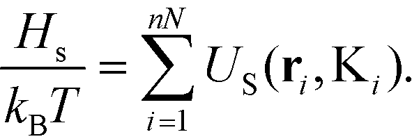
The simulation results presented here are based on the standard coarse-grained model for block copolymers.16 Previous work has relied on this model to elucidate the morphological behavior of block copolymer films on chemically and topologically patterned substrates and results have been quantitatively consistent with experimental observation.17–20 Polymers in the model are represented by flexible, linear Gaussian chains discretized into N beads, where the position of the sth bead in the ith chain is given by the vector ri(s). A system is composed of n AB copolymer molecules in a fixed volume V at a fixed temperature T. The Hamiltonian H = Hb + Hnb + Hs of the system includes the interactions between bonded beads (b), the non-bonded interactions (nb), and the interaction of beads with the substrate (s). The connectivity of neighboring beads in a polymer chain is modeled by describing the bonded interactions acting along the chain by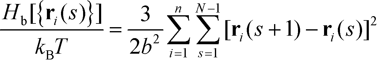 | (1) |
 | (2) |
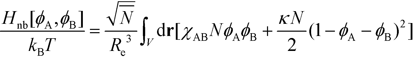
 represents the invariant degree of polymerization, which is proportional to the polymer's molecular weight in a dense melt, and ρ0 is the bead number density. The local dimensionless density ϕK of species K = A, B is computed using the configuration of the polymer beads relative to a lattice with spacing ΔL using a zeroth-order particle-to-mesh interpolation. The incompatibility between unlike species is measured by the Flory–Huggins parameter, χABN, and the inverse isothermal compressibility, κN, gives the polymer melt a finite compressibility.
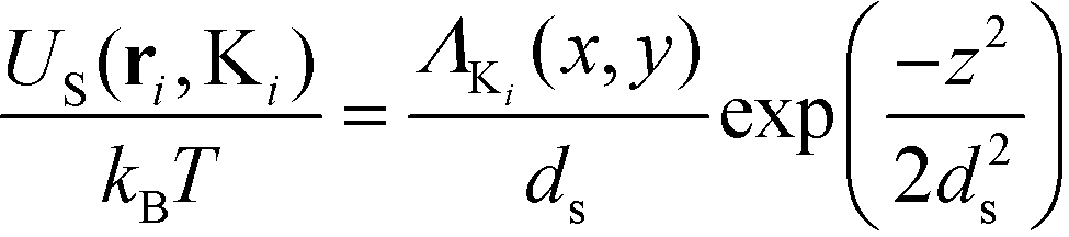
To model the experimental systems used for DSA of block copolymers, the polymer is confined between two impenetrable walls normal to the z-axis of the simulation box. The top wall at z = Lz is considered neutral, whereas the bottom wall at z = 0 mimics the chemically patterned substrate on which the block copolymer assembles. The interaction between the substrate and polymer is modeled by a one-body potential acting on each bead of the form
 | (3) |
 | (4) |
Λ K represents the strength of the interaction between polymer beads of type K = A, B located at (x, y) and the substrate. The functional form of ΛK is dependent on the geometry of the chemical pattern.
Monte Carlo (MC) simulations are used to identify possible self-assembled morphologies over certain chemical patterns. Configurations are sampled according to the Metropolis criteria, where the probability of accepting a trial configuration is given as Pacc = exp(−ΔH/(kBT)), and where ΔH represents the energy difference between the original and proposed configurations. Trial configurations are produced using four different Monte Carlo moves: single bead displacement, translation of a chain, chain reptation, and chain inversion.
The polymer melt considered here is characterized by the parameters  , κN = 22 and χABN = 17 which correspond qualitatively to AZEMBLY™ PME312 used in the experiments at IMEC. The lattice for computing local densities is defined such that the average number density of beads in any cell is nint = 14. The computed bulk domain spacing of the melt using these simulation parameters is L0 = 1.5Re. We choose ds = 0.05Re to ensure that the interaction between the patterned substrate and the polymer operates in a range similar to that of the incompatibility between blocks. The underlying chemical pattern is composed of repeated stripes of width W that have a period LS. The area between stripes is referred to as the backfill region. The guiding stripes' strength of interaction with the polymer is denoted by ΛS and the backfill interaction by ΛB. A larger value of ΛS indicates a greater affinity of the stripes for the A-type polymer (PS), where a larger value of ΛB indicates a greater affinity of the backfill for the B-type polymer (PMMA).
3 Results
The chemo-epitaxy flow for directed self-assembly (DSA) of block copolymers (BCPs) designed by Liu and Nealey (LiNe flow), shown in Fig. 1, was used to assess the combinatorial effect of the composition and the dimensions of the chemically nano-patterned substrate on the assembly process. We used the fully automated process implemented on industrial equipment available at IMEC. First, a thin film of X-PS was coated onto a SiN layer deposited on 300 mm silicon wafers. Next, a photoresist layer was coated and exposed using 193 nm immersion lithography. The mask used for this work includes gratings of various pitches and a large patterned area of LS = 84 nm. A matrix of focus and exposure doses (FEM) was used to print line/space patterns with varying critical dimension (CD). After exposure and development, a dry etching process was used to simultaneously tune the width of the photoresist lines and remove the X-PS exposed to the plasma. In the next step, the remaining photoresist was rinsed with organic solvent, yielding X-PS guiding stripes. A series of OH-terminated brushes of specific composition were used to functionalize the area between the X-PS lines, often referred to as the backfill region, via a condensation reaction of the hydroxyl-end groups and the oxygen moieties incorporated in the surface during the etching step. On these chemical patterns of defined geometry and chemistry, a BCP film was coated and annealed. After the removal of the PMMA block, the resulting structures were imaged and related to the boundary conditions used in each case.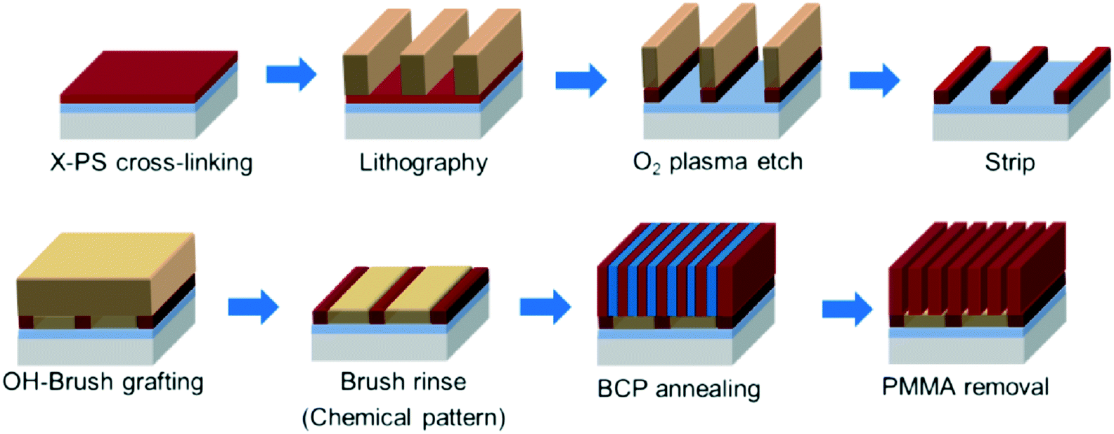 | ||
| Fig. 1 Liu–Nealey (LiNe) flow for the fabrication of chemically nanopatterned substrates with well-defined geometry and chemistry, and subsequent DSA of a symmetric BCP. | ||
In the fabrication of the chemical patterns, the X-PS is the first polymer applied on the SiN layer, which further underwent photoresist exposure, a trim-etching procedure, stripping of the photoresist, and brush deposition before coming into contact with the BCP material. In order to gain insight into the wetting properties of the guiding stripe relative to the unmodified X-PS, we assessed the impact of each of these steps on the chemical character of the X-PS prior to the construction of the final guiding feature. Due to the dimensions of the guiding stripe, direct evaluation of the wetting properties of the process-modified X-PS was difficult. Therefore, we created surfaces that were representative of the X-PS at each processing step. To achieve these model surfaces, we coated and annealed an X-PS and a photoresist layer onto a Si wafer with the same conditions described for the fabrication of the chemical patterns. On these substrates, checkerboard patterns, which consist of exposed and unexposed regions that are approximately 3 cm × 3 cm, were exposed using conventional illumination and an energy of 18 mJ cm−2. The printed areas are sufficiently large to allow for the measurement of the water contact angle (WCA) of each surface. The wafers were subsequently trim-etched, stripped, and coated with the different brushes to reproduce surfaces consistent with the X-PS at each step in the process of producing the chemically nanopatterned substrates. Water contact angle results for a blanket X-PS film and the unexposed and exposed areas on the checkerboard patterns that were processed prior to brush grafting are shown in Fig. 2.
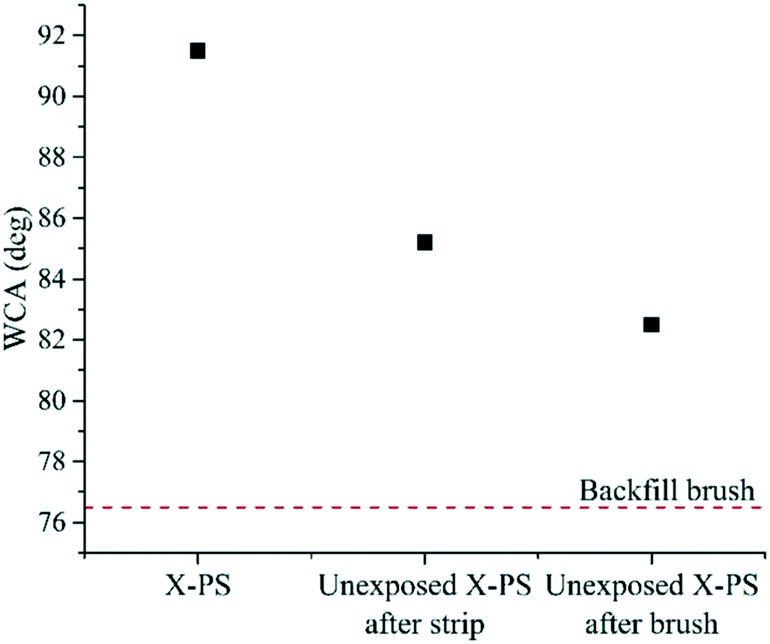 | ||
| Fig. 2 Water contact angle measurements of an X-PS film as coated and annealed, after resist stripping, and after brush grafting, show the change in the wetting properties of the X-PS at each processing step in the creation of the chemically nanopatterned substrate. | ||
Each processing step made the X-PS film more hydrophilic. The first decrease in the WCA can be attributed to the degradation of the X-PS by the ultraviolet light generated during the exposure and the Cl2 plasma during the trim-etching step.21–23 Further optimization of the trim-etching step may provide an alternative route to retain the hydrophobic character of the X-PS and increase the strength of the interaction between the guiding stripe and the BCP domains.
The second decrease in the WCA after P(S-r-MMA)-OH coating and annealing suggests that the brush molecules can partially graft to the guiding stripes. This may be an additional consequence of the modification of the X-PS, by UV irradiation, with oxygen-containing functionalities, which can further react with the hydroxyl end group of the random copolymer. At the end of the process, the unexposed X-PS presented a WCA of 82.5°, as shown in Fig. 2. A total drop of nine degrees in the WCA indicated that the X-PS guiding stripe lost some of its non-polar character, resulting in a weaker expected interaction with the BCP. For the present analysis, this is advantageous, as previous reports using the LiNe flow, as described in this study, show assembly of the BCP with a high degree of perfection, suggesting that the difference in interfacial energy between the X-PS and the backfill region with PS and PMMA is large enough to guide the BCP structures over thin (W/L0 ≈ 0.5) and wide guiding stripes (W/L0 ≈ 1.5). In contrast, a strong interaction with the guiding region may yield non-bulk morphologies during BCP assembly, especially for wide guiding stripes (W/L0 > 0), which may limit the range of dimensions of the chemical patterns available for our investigation.24,25
One important aspect of the LiNe flow is its brush-last approach, which ensures that the surface properties of the backfill area are exclusively controlled by the material design of the random copolymers grafted to this region. Therefore, before incorporating the P(S-r-MMA)-OH random brushes into the chemical nano-pattern, we measured the film thickness and WCA of each brush material, thereby gaining insight into the topographical and chemical nature of the patterned substrates. First, we coated blanket wafers with each unique brush and annealed them to tether the molecules to the substrate through the hydroxyl end group via the condensation reaction mentioned previously. Excess material was rinsed, yielding a monolayer that was chemically grafted to the surface. The film thickness and uniformity across the wafers were characterized using ellipsometry. Independent experiments by varying the annealing time and temperature have demonstrated that a saturated monolayer of a random copolymer brush with fPS = 0.51, which is similar to the standard Brush-51 used in the experiments presented in this work, is about 7 nm.26 We performed ellipsometry measurements on the AZEMBLY® series used in this work to provide accurate film thicknesses for the particular batch of materials used in the experiments shown. Fig. 3a shows the film thickness results obtained for the investigated AZEMBLY® brushes; each measurement was performed on brushes that had the same initial film thickness and annealing conditions. The thinnest film was observed with Brush-51 where the thickness was measured to be 5.2 nm, while Brush-60 produced the thickest film of 8.0 nm. The difference of the brush thickness used in this work and the values obtained previously can be attributed to the different batches of materials used. In addition, we measured the thickness of a blanket X-PS film to be 7.2 nm. The difference between the thicknesses of the blanket X-PS and each unique brush film suggests that there were minimal topographical features on the final patterned substrates.
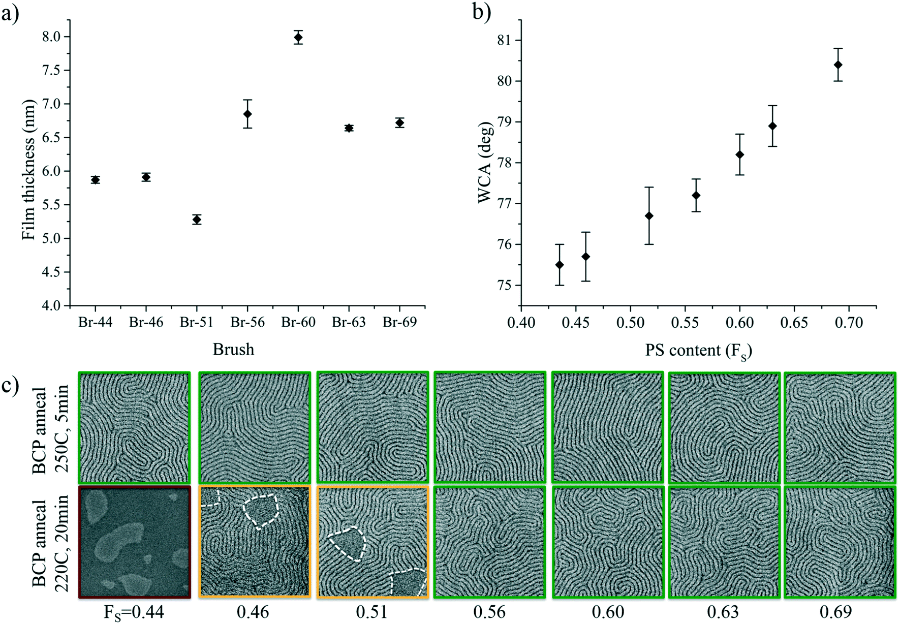 | ||
| Fig. 3 Characterization of a series of brushes with different compositions: a) monolayer film thickness after rinse as determined by ellipsometry measurements, b) water contact angle measurements, and c) top-down SEM images of P(S-b-MMA) films annealed at 220 °C and 250 °C on top of the different random brushes grafted onto silicon wafers. The green squares indicate the brushes that result in perpendicular BCP assembly, while yellow and red frames indicate mixed orientation and hole–island assemblies, respectively. | ||
The chemically modified surfaces were subsequently used to perform static WCA measurements. Fig. 3b shows that the series of brushes exhibit a monotonic increase in WCA as fS increases, with values that are in agreement with previous reports.11 For the current study, in which the chemical patterns were composed of an X-PS guiding stripe, Liu et al.6 demonstrated that the optimal brush in the backfill region must be slightly preferential for PMMA. Therefore, in order to test the wetting properties of the substrates treated with each brush material, a 32 nm film of BCP was coated onto the samples and annealed at 250 °C for 5 min or at 220 °C for 20 minutes. As shown in Fig. 3c, when the BCP was annealed using standard conditions (250 °C, 5 min), all the samples showed perpendicular assembly of randomly oriented structures. However, at the lower temperature, mixed orientation was observed as the PS content in the brushes decreased. At the lowest end, Brush-44 showed hole-and-island structures characteristic of preferential wetting of one of the blocks to the substrate. In contrast, the higher PS content in the brush materials (≥56% PS) did not induce mixed or parallel orientation of the polymer domains. These results suggest that the composition of the brush series available in this study provides the wetting properties of interest, ranging from slightly preferential for the PMMA block to non-preferential.
The response of the BCP assembled on chemically nanopatterned substrates of different compositions and dimensions was also investigated. The impact of the commensurability of the pattern period with the natural domain spacing of the BCP (LS/L0) and the width of the guide stripe (W/L0) was studied by varying these parameters through the exposure and etching conditions, as described previously.26 In addition, the interfacial energy between the PS and PMMA blocks with the backfill region was included in this analysis by using brushes of different compositions. In order to investigate the BCP behavior over large areas, the 84 nm inspection blocks included from the reticle design were imaged using top-down SEM at ten different locations under each exposure condition. A total area of 62.5 μm2 per die was imaged and used to evaluate the defect level through the patterned region. The number of defect-free images is reported as a measure of the degree of order, where a value of 10 indicates that all ten images taken had zero visible defects. This method does not differentiate between random orientation and a single dislocation; however, we can identify the pattern conditions that thermodynamically favor well-registered assembly (WRA) such that no misaligned structures exist after DSA. The results collected from ten dose steps at nominal focus with 12.6 < W < 35.6 nm for the available brushes are shown in Fig. 4. Random orientation or partial alignment, indicated by the red and yellow squares, respectively, was observed for all brush compositions when W ≤ 13.0 nm, indicating that the guiding stripe is not wide enough to direct BCP assembly. As W increases, good registration of the BCP with the underlying chemical pattern, represented by the green squares, was observed when 14.8 ≤ W ≤ 27.3 nm on the samples treated with brushes of low fS (0.44–0.51). In contrast, the images collected for large PS content random copolymers (>56% PS) showed a drastic reduction of the process windows for the same guiding stripe width range. When W = 32 nm, random orientation is observed for all brush compositions. This result is in good agreement with previous reports, where the lack of registration with the guiding material when W/L0 = 1.0 was related to the largest total free energy of the system calculated under this condition. Finally, as W/L0 approached 1.5, the material that resulted in the largest number of defect-free images was Brush-51, although, in all cases, the process window was significantly smaller than the window for thinner stripes.
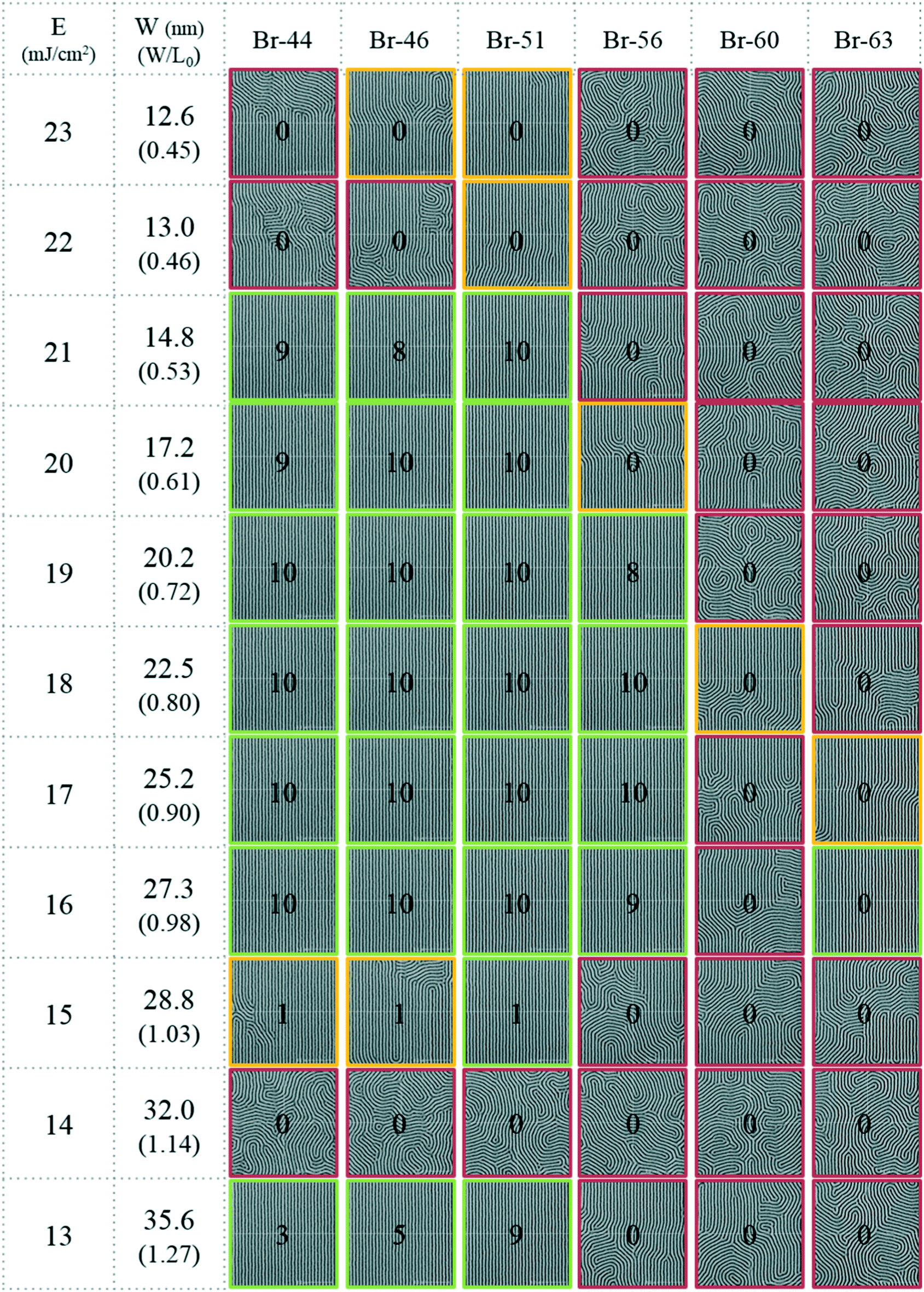 | ||
| Fig. 4 Top-down SEM images of a BCP assembled on chemical patterns with different W and backfill brush compositions over a pattern with an 84 nm pitch. The number on each die represents the number of defect-free images out of ten images analyzed. | ||
In order to include the impact of the commensurability of the pattern period with the natural domain spacing of the BCP (LS/L0) in our parameter space, we evaluated the degree of order of the BCP structures assembled on chemical patterns of different LS, W, and backfill brush compositions. To this end, top-down SEM images of 2.5 μm × 2.5 μm areas (1 μm × 1 μm are shown in Fig. 5 to exemplify the scoring system) were assigned a score according to the degree of order observed under each condition. Ten random images, each of a 2.5 μm × 2.5 μm area, from each pattern design were investigated manually by eye to score the pattern. A range from 0 to 3 was used, corresponding to random orientation to a high degree of order, respectively. If at least nine of the ten images under the conditions showed no defects, then the pattern design was scored a 3. If a fingerprint assembly was observed in all ten images, then the pattern was scored a 0. A score of 2 indicates that only isolated defects were observed, while a score of 1 indicates that, among the ten images analyzed, a combination of images of fingerprint assemblies and images of assemblies containing isolated defects was observed. This scoring system provides a qualitative experimental metric for the thermodynamic stability of a WRA compared to a misaligned structure. A score of 3 indicates that there is a large enough difference in the free energy of the WRA and a misaligned domain that no other grains can be found in any field of view. In contrast, a score of 0 indicates that the free-energy difference between all possible states is small, such that the field of view will consist of multiple grains. We identify a thermodynamic process window using this metric, by finding the conditions that produce SEM images with a score of 3.
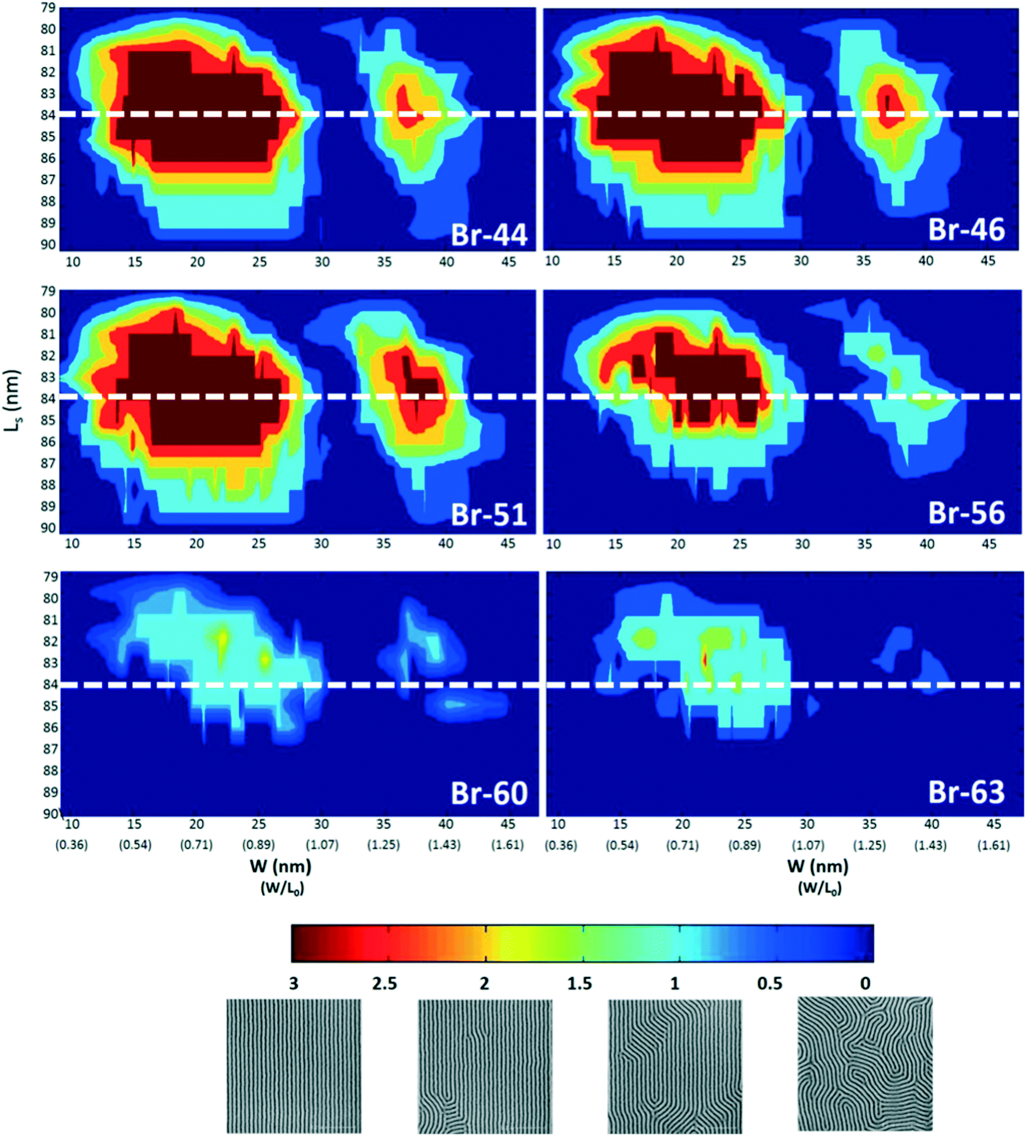 | ||
| Fig. 5 BCP assembly as a function of pitch (LS) and width of the guiding stripe (W) for various compositions of the backfill brush. The color code used to evaluate the degree of perfection of the assembled structures is based on a 0–3 score system corresponding to random orientation to good alignment, respectively, as shown by the top-down SEM images. The dashed, white lines indicate the pitch that is commensurate with 3× density multiplication. | ||
Fig. 5 shows these experimentally determined thermodynamic process windows in W/L0 and LS for patterns with different brushes. For the standard backfill material, Brush-51, the largest thermodynamic process windows in W occurred using a pattern with a commensurate pitch of 84 nm, where LS/L0 = 3.0. In addition, it can be observed that the BCP can accommodate different pitches in the range of 81 nm ≤ LS ≤ 86 nm, with slightly higher tolerance for compression compared to stretching.
In terms of W, two process windows were obtained, in agreement with the observations over large patterned areas and with previous results. The largest window is observed when W/L0 < 1.0 (12.4–27.0 nm). Process windows of similar size were observed at small values of W/L0 for the chemical patterns with low fS (0.44–0.46) grafted to the background. Still, Brush-51 showed more tolerance towards incommensurate chemical patterns, at both small and large pitches. Increasing the PS content of the brush to fS = 0.56 caused shrinkage in these process windows. The brushes with the higher PS content (Brush-60 and Brush-63) showed an even greater reduction in the process window size, such that only partial alignment was captured from the top-down SEM images. As W/L0 approaches 1.0, the top-down SEM images show fingerprint patterns on all chemical patterns with different LS and brush compositions. Finally, a second smaller process window is observed as W/L0 approaches 1.5 (36–40 nm). As with the process window observed over thin guiding features, the more PMMA-preferential brushes show combinations of W/L0 and LS that produce a WRA, but this window begins to disappear for brushes with fS > 0.56. The results for Brush-69 are not shown because random orientation of the assembled BCP was observed on most samples. These trends in thermodynamic process window size indicate that a PMMA-preferential backfill of the pattern is necessary to create conditions that thermodynamically favor a WRA enough to have no other grains present in the final assembly for both thin and wide guiding stripes.
Experimental data were compared with simulation results to gain insight into the effect that the chemical nature of a patterned substrate has on the DSA process of lines-and-spaces. The simulations presented here focus on chemically patterned substrates that result in 3× density multiplication which is comparable to the guiding patterns used in our experimental work. We investigate the impact that three parameters characterizing the chemical pattern have on the assembly of the block copolymer: guiding stripe width, guiding stripe's preference for the guided species PS, and the backfill's preference for the non-guided species PMMA. While film thickness is a key parameter in the resulting assembled morphology, here it is fixed at a value of Lz = 1.28L0 in all simulations, which is comparable to the experimental conditions, where the thickness of the AZEMBLY™ PME312 films assembled on the chemical patterns is approximately 32 nm.
In experiments, there is a wide range of unwanted structures that form over patterns where the final assembly would be categorized as 0, 1, or 2 in Fig. 5. A commonality amongst many of the defective structures observed in the SEM images analyzed earlier is the presence of lamellar grains that are misaligned with respect to the underlying pattern and appear to be oriented perpendicular to the substrate. Fig. 6 shows an SEM image depicting the fingerprint registration of the block copolymer, which is a combination of the coexistence of many grains in one assembly, over a chemical pattern. The areas of misaligned lamellae can be of various sizes, and Fig. 6 shows examples of areas of grains that are at least as large as the simulation box (6L0 × 6L0). As a first approximation of a pattern's effectiveness for guiding a DSA process, we look at the thermodynamics of different grain orientations to the underlying patterned stripes. We investigate the relative thermodynamic stability of grain orientations over different patterns using thermodynamic integration to calculate the free energy of the metastable morphologies (with methodologies previously utilized with the TICG model).24,27 We initialize the simulations such that the block copolymer is a microphase separated into lamellae that are perpendicular to the underlying substrate and form an angle θ with the underlying guiding stripe, which we refer to as a misaligned grain (MG) (see Fig. 6). We refer to the case where θ = 0.0° as a well-registered assembly (WRA), which is the case where the grain is aligned with the patterned features. The simulations are allowed to relax over 5 × 10⁵ MC sweeps to produce metastable morphologies that appear, from a top-down view, to be lines-and-spaces oriented at θ degrees with the guiding feature.
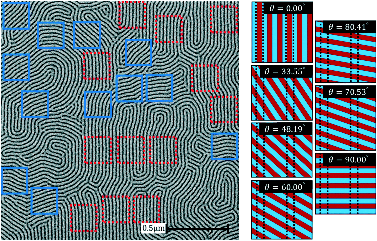 | ||
| Fig. 6 On the left is an SEM image of P(S-b-MMA) assembled atop a chemical pattern composed of guiding stripes for production of lines-and-spaces using density multiplication. A subset of grains that are approximately the size of a simulation box is identified. Areas of the final assembly with misaligned grains are shown within solid blue boxes, while areas with a well-registered grain are within dashed red boxes. Each box has dimensions 6L0 × 6L0. The tiled images on the right show cartoon schematics of the possible angles of rotation, θ, of a lamella for two pattern periods. The angles are calculated assuming that the average spacing of the lamella is equal to the natural bulk domain spacing, L0. The dashed, black lines indicate the location and orientation of guiding stripes. | ||
We could only investigate grains at a discrete number of angles θ due to the periodic boundary conditions of the simulation box. By assuming that the block copolymer adopts the natural bulk domain spacing on average, we are able to investigate 3P + 1 values of θ, where P is the number of chemical pattern periods contained in a simulation box. A value of P = 2 was used in this work, as the increased resolution in θ for P > 2 increased the computation time. In addition, there are instances in the experimental SEM images where grains of the same size as a box with P = 2 can be found, as shown in Fig. 6. The values of θ and a schematic demonstrating the assembly over the chemical patterns for each value can be seen in Fig. 6. For each simulation of a misaligned grain, the simulation box has a height of Lz = 1.28L0 and the box-dimension normal to the direction of the underlying pattern is 6L0, such that each simulation contains two periods of the chemical pattern. The third dimension of the box is chosen such that the initialized microphase separated domains have a period of 1.0L0. The third dimension for the WRA is always 6.0L0. We then perform thermodynamic integration to compute the difference in free energy, ΔF, between an assembly of defect-free lamellae perpendicular to the substrate that is oriented at an angle θ to the chemical pattern and a defect-free lamella with period 1.0L0 confined between two neutral surfaces.
In order to demonstrate the described methodology, we investigate the impact of the guiding stripe on the relative free energy of different orientations of assembled lamellae. We selected a chemical pattern with a guiding stripe with strength ΛS = 0.75 and a backfill with strength ΛB = 0.20. We calculated the relative free energy for the seven orientations of assembly shown in Fig. 6. Fig. 7 shows the comparison of free energy between the WRA and the misaligned orientation with the lowest free energy, which we refer to as the most competitive assembly (MCA). Noted that all of the misaligned orientations have similar energies, but for the purposes of this work, only the orientation with the absolute lowest free energy was considered as the MCA. The free energy of the MCA changes linearly with guiding stripe width. The MCA for each W/L0 may correspond to different rotations of the misaligned grain. This trend can be explained by analyzing the structure of the misaligned assemblies, which adopt a morphology that consists of lamellae that are deformed in close proximity to the substrate. In these assemblies, wetting layers of the guided material and unguided material form over the guiding stripe and the backfill, respectively. The larger interfacial energy of the guiding feature (ΛS > ΛB) leads to higher interfacial curvature of the lamellar domains over the guiding stripe than that over the backfill due to this wetting behavior. The change in guiding stripe width does not cause a qualitative change in the assembly for these rotated lamellae; however, the increase in the volume of polymer that interacts with the guiding feature results in an increase in the fraction of lamellae with larger interfacial curvature, resulting in the observed change in free energy of these structures with guiding feature width.
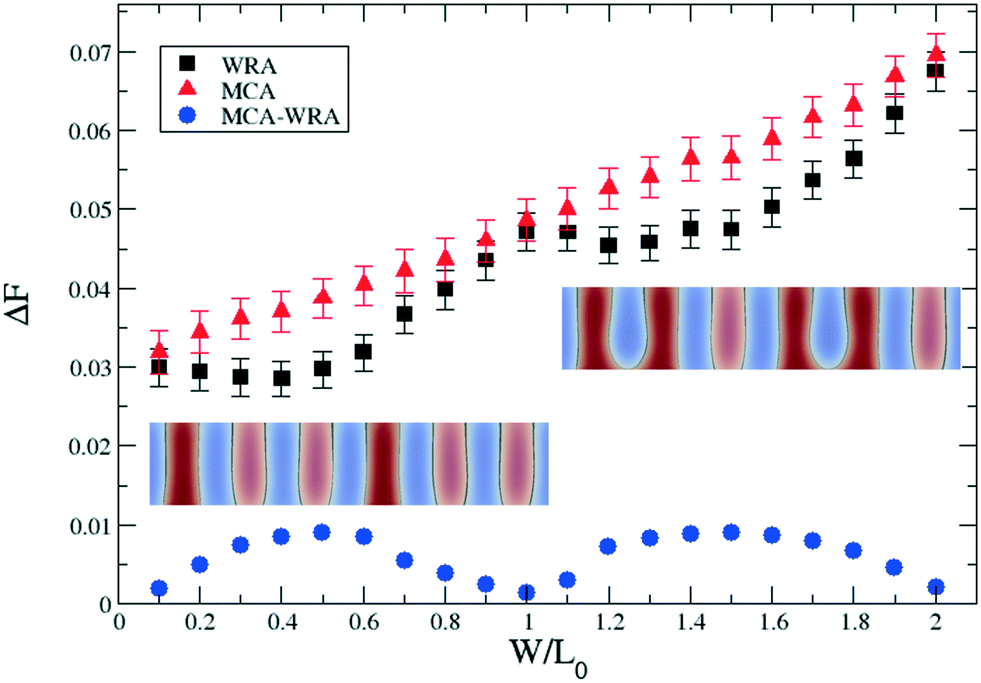 | ||
| Fig. 7 The red triangles and black squares show the calculated ΔF in kBT/chain for the well-registered assembly and the most competitive assembly, respectively, over periodic guiding stripes of width W at a pitch of LS/L0 = 3.0 for ΛS = 0.75 and ΛB = 0.2. The blue circles show the difference in the relative free energy of the WRA and the MCA for the corresponding stripe width using ΔΔF = ΔFMCA − ΔFWRA. The insets show the through-film profile of the WRA at two different guiding stripe widths, W/L0 = 0.5 and 1.5. The guided domains are identified in dark red. | ||
In contrast, a WRA has a fundamentally different structure over thin and wide guiding stripes. The differences between the two types of structures are demonstrated in the insets in Fig. 7. For thin guiding stripes, 0 < W/L0 < 1.0, the assembly is characterized by a guided block (species A) domain centered over the stripe, while the wider guiding features, 1.0 ≤ W/L0 < 2.0, have a non-guided block (species B) domain centered. The difference between these two types of assembly causes a more complicated trend in free energy versus guiding stripe width than that of the misaligned assemblies. The ΔF of the WRA over these chemical patterns results from three interactions: the amount of non-guided material (species B) affected by the guiding stripe, the amount of guided material (species A) affected by the backfill, and the curvature of the AB interface. Greater volumes of non-guided material assembled over the guiding stripe and guided material assembled over the backfill result in a larger enthalpic contribution to the free energy of the assembly. Meanwhile, larger interfacial areas between A and B domains are associated with a larger entropic contribution.
In addition, Fig. 7 shows the difference in ΔF associated with the WRA and the MCA, ΔΔF = ΔFMCA − ΔFWRA, for the defined patterned substrate with a slightly weak guiding stripe and a slightly preferential background region. ΔΔF provides a measure of thermodynamic preference of the chemical pattern for the desired assembly, the WRA. Fig. 7 shows the local maxima in ΔΔF at W/L0 = 0.5 and 1.5. These are the optimal guiding stripe widths for having the highest thermodynamic preference for a WRA over a misaligned grain for the two fundamentally different assemblies mentioned earlier with the chosen interfacial energies (ΛS = 0.75, ΛB = 0.20). Although these two values of W/L0 have a different material centered upon the guiding feature and the interfacial curvature of the assembled domains is drastically different, the relative values of ΔΔF at W/L0 = 0.5 and W/L0 = 1.5 in Fig. 7 indicate that the two patterns provide equivalent selectivity for the assembly that appears to be well registered to the underlying pattern from a top-down perspective. This is a rare situation, where the selectivity is approximately equal under the optimum conditions within each processing window. Fig. 9 shows that, for most interfacial energy combinations, the selectivity for a WRA is higher for thinner guiding features. While the thermodynamics may indicate that both guiding patterns have the same preference for a WRA over other grain orientations, the nature of the WRA is different and must be considered when designing experimental conditions for industrial applications, as the increased curvature could change the way the assembly affects post-DSA processing.
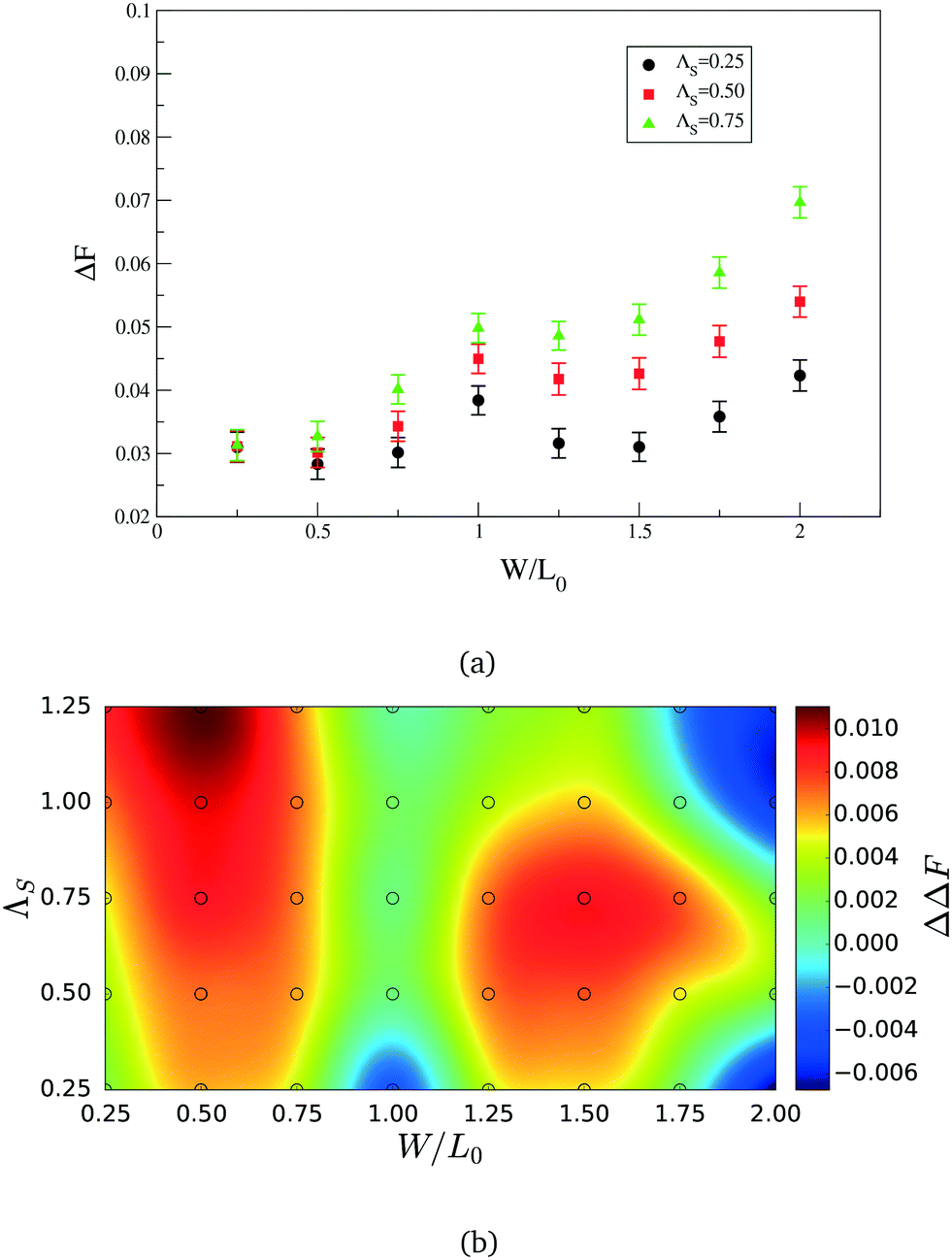
In order to better understand the effect of substrate chemistry on DSA, we also examine the guiding stripe affinity for the material to be guided. We fix ΛB = 0.2, which models a backfill region that is slightly preferential for the non-guided material. This strength of the guiding stripe ΛS was varied from 0.25 to 1.25 in 0.25 increments and W/L0 was varied from 0.00 to 2.00 in 0.25 increments. The same procedure as outlined above was performed to calculate the ΔF and ΔΔF for each set of parameters. Fig. 9 shows the ΔF vs. W/L0 of the WRA and the MCA for three of the five different ΛS values evaluated. For the thinnest guiding stripes with W/L0 = 0.25, there is no statistically significant difference in the free energy of the WRAs between the three guiding stripe strengths. The increased strength is an increase in repulsion of the non-guided material, therefore the enthalpic energy of the system is only increased when the B species interacts with the guiding stripe. Stripes at this width only interact with one A-type domain in a WRA and increasing ΛS does not cause a significant change in the ΔF because the A-preferential surface only interacts with the small amount of non-guided material that is present in the singular A-rich domain centered on the stripe. Fig. 8 compares the change in interfacial area for different interfacial energies at various guiding stripe widths through a normalized interfacial area, σ. This value is calculated by obtaining the average surface area of the interface between A and B domains in one period of the pattern, LS, obtained from simulations at equilibrium and normalizing that value by the idealized surface area that would exist if each domain were a rectangular prism. The value of σ is never calculated to be 1.0 due to the molecular fluctuations present in the TICG model. However, it can be seen in Fig. 8 that a larger value of ΛS causes no statistically relevant change in the average interfacial area of WRA over guiding stripes of width W < 0.8. This results in WRAs that are equivalent in relative free energy, as the structures of the assemblies are approximately identical. Larger stripes have more interactions with the B-species, resulting in more perturbation to the WRA, and a larger ΔF. However, rotated assemblies invariably have fractions of the guiding stripe covered by the B-rich domain. The larger repulsion of the B-species that comes with stronger guiding stripes results in increased wetting of the stripe by the A-species which causes an increase in the curvature of the AB interface. The extra frustration due to a larger amount of curvature at stronger guiding stripes causes the ΔF of these rotated assemblies to increase. The heat map in Fig. 9b shows that stronger thin guiding stripes caused an increase in ΔΔF for the ΛS investigated due to the minimal impact that ΛS has on the WRA and the higher amount of perturbation of the MCA associated with a stronger stripe.
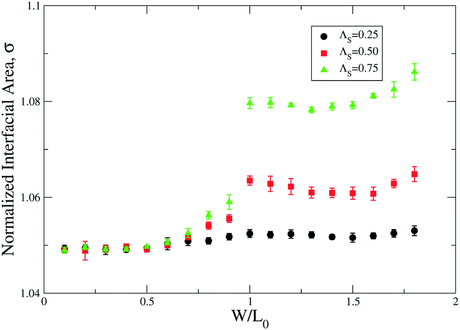 | ||
| Fig. 8 Normalized interfacial area, σ, of a WRA over periodic guiding stripes of widths W/L0 ∈ [0.5, 1.5] with pitch LS/L0 = 3.0. The value of σ is found by comparing the interfacial area between A and B domains calculated from simulations of a WRA at equilibrium with the calculated A–B interfacial area that would exist if all A and B domains were rectangular prisms. | ||
 | ||
| Fig. 9 a) The relative free-energy difference ΔF in kBT/chain of the WRA as a function of guiding stripe width, W/L0, for the guiding stripe strengths ΛS = 0.25, 0.75 and 1.25 and ΛB = 0.2 for a pattern with periodicity LS/L0 = 3.0. b) A heat map showing the difference in ΔF for the WRA and the MCA as a function of guiding stripe strength, ΛS and W/L0, where ΔΔF = ΔFMCA − ΔFWRA. | ||
For wide guiding stripes, where W/L0 > 1.0, the presence of a B-domain over the guiding feature changes the trend in ΔΔF associated with a higher preference of the stripe for the guided material. The preference of the stripe for the guided material causes wetting of the stripe by the A-species, which leads to the larger interfacial curvature of a WRA over guiding stripes of width W/L0 > 1.0 shown in Fig. 8; at high values of ΛS, the B-rich domain becomes completely disconnected from the substrate. This wetting behavior creates more frustration in a WRA over stronger guiding stripes, as can be seen by the increase in ΔF of the WRA over wide stripes for higher ΛS in Fig. 9. Although the trends in ΔF for well-registered assemblies are different for thin and wide guiding stripes, the trend for the rotated assemblies remains the same in both regimes of stripe width. The maximal ΔΔF over wide guiding stripes was obtained at ΛS = 0.75 for the strengths investigated. For the values of ΛS > 0.75, there is a decrease in ΔΔF indicating that the frustration caused by the wetting behavior in the WRA causes the rotated morphologies to become more competitive. It should be noted that, at values of ΛS > 1.25, the WRA is no longer even metastable, and the simulations predict assemblies of non-bulk morphologies where the guiding stripe is completely wet by the preferred block. The decrease in ΔΔF and the instability of a WRA at high values of ΛS indicate that the interfacial energy must be more tightly controlled for wide guiding stripes.
These results indicate that a value of ΛS in the range between 0.5 and 0.75 qualitatively agrees with the experimental results, as Fig. 9 shows that these two values of ΛS have high selectivity for a WRA at thin and wide guiding stripes. The simulation results, presented in Fig. 9, suggest that optimizing the processing conditions to retain the hydrophobicity of the unmodified X-PS could lead to greater thermodynamic selectivity for the BCP to assemble with a high degree of perfection and improve the process over thin guiding stripes. In contrast, Fig. 9 also demonstrates that using a more selective material could result in worse conditions for producing a WRA when using wide guiding stripes. In summary, the largest possible ΔΔF between a WRA and its corresponding MCA, which will lead to a minimum number of defects, will occur at W/L0 = 0.5. However, if due to resolution limits or fabrication constraints such dimensions are difficult to achieve, then a guiding stripe with W/L0 = 1.5 and weaker interaction with the blocks may still result in a WRA with a high degree of perfection.
The selectivity of a guiding pattern for WRAs is also influenced by the choice of material used in the backfill area, as shown in the experimental work. The periodicity of the pattern was set to LS = 3.0L0, so as to compare it directly with the width of the thermodynamic process windows in Fig. 5. We chose to fix ΛS = 0.75, as the guiding stripe chemistry remained constant in the experimental work, and investigated backfill strengths of ΛB = 0.0, 0.2 and 0.4 with W/L0 from 0.0 to 1.5 in increments of 0.1. This is not a comprehensive exploration of guiding chemistries, but it does give insight into the influence of the backfill interfacial energy on the assembly. Fig. 10 shows that, for both thin and wide guiding stripes, increasing ΛB results in a larger ΔΔF. A backfill that is more preferential for the non-guided material results in a larger ΔF of the WRA due to increased AB-interfacial curvature that results from the wetting behavior of the B-species on the backfill. In addition, stronger backfills cause an increase in the ΔF of the MCA, for the same reason. For every guiding stripe width investigated in Fig. 10, the MCA is more sensitive to backfill affinity because the geometry of a rotated assembly ensures that a larger fraction of the B-rich domain assembles atop the backfill region. This indicates that increasing the affinity for the backfilled area for the non-guided material leads to an increased thermodynamic stability of a WRA relative to a misaligned grain. It should be noted that the backfill can be too preferential, such that parallel lamellae become the preferred state, especially for thin guide stripes. However, for moderate values of ΛB, molecular simulations demonstrate good agreement with experimental findings, where patterns with PMMA-preferential backfills show greater thermodynamic selectivity for a WRA compared to a misaligned grain.
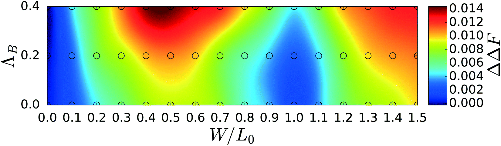 | ||
| Fig. 10 A heat map showing the difference in ΔF for the WRA and the MCA as a function of backfill strength, ΛB and W, where ΔΔF = ΔFMCA − ΔFWRA. The guiding stripe strength is maintained at a constant value of ΛS = 0.75 and the pitch is fixed at LS = 3.0L0. | ||
4 Conclusions
The implementation of a chemo-epitaxy flow in an industrial fabrication facility allowed for the systematic investigation and precise control of critical characteristics of chemically nanopatterned substrates. We focused specifically on the effects of the guiding stripe width, guiding stripe affinity for the PS, and backfill affinity for PMMA with a 3× density multiplication pattern that was commensurate with the bulk domain spacing of the block copolymer. Two fundamentally different process windows that assembled single grains with a high degree of perfection were identified using top-down SEM images. A new strategy that relies on molecular simulations supported the existence of these process windows by demonstrating maximum thermodynamic driving force for a well-registered assembly when compared to a competitive misaligned grain at W/L0 = 0.5 and 1.5. Free-energy calculations also demonstrated that increasing the affinity of a thin guide stripe for PS increases the thermodynamic selectivity for a single grain aligned with the underlying pattern. The selectivity can be increased for wide guiding stripes, W/L0 = 1.5, by having a higher affinity of the stripe for the guided material; however, if this affinity is too large for these stripe widths where the unguided material is centered over the guiding stripe, then the selectivity is reduced until the WRA ceases to be metastable. Experimentally, the size of these process windows was adjusted by changing the composition of the backfill brush. As the PS content in the brush decreased, the two process windows in W increased in size. Similarly, we showed through simulations that a backfill that is more preferential for PMMA would have a higher thermodynamic selectivity for the WRA. The results presented here provide a justification for engineering rules that can be used for designing patterns. Although this study does not consider important kinetic aspects of the assembly process, we speculate that by tailoring the interfacial energies and guiding stripe widths according to the rules proposed here, such that the thermodynamic driving force is maximized, patterns can be designed which are more suitable for meeting industrial defect requirements. We finish by emphasizing that when assessing a chemical pattern for industrial application, the through-film structure must be considered alongside the ease of producing what appears to be the desired assembly from a top-down perspective, and here we also showed that 3D structures can have curvature that may not be noticeable from top-down inspection.Conflicts of interest
There are no conflicts to declare.Acknowledgements
The preparation of DSA samples and the analysis of the data were supported by the NSF Scalable Nanomanufacturing Program. The development of industrially-relevant strategies for next-generation lithographic patterning was supported by the Semiconductor Research Corporation. The development of model-based strategies for design of engineering processes based on molecular optimization and interpretation of high-information-content data was supported by the Center for Hierarchical Materials Design. The authors are grateful to IMEC for use of the inspection tools and assembly lines available at their Belgium facility, and to the Research Computer Center at the University of Chicago for providing the necessary computing resources.References
- F. S. Bates and G. H. Fredrickson, Phys. Today, 1999, 52, 32 CrossRef CAS.
- M. P. Stoykovich, H. Kang, K. C. Daoulas, G. Liu, C. C. Liu, J. J. De Pablo, M. Müller and P. F. Nealey, ACS Nano, 2007, 1, 168–175 CrossRef CAS PubMed.
- S. O. Kim, H. H. Solak, M. P. Stoykovich, N. J. Ferrier, J. J. De Pablo and P. F. Nealey, Nature, 2003, 424, 411–414 CrossRef CAS PubMed.
- C. C. Liu, E. Han, M. S. Onses, C. J. Thode, S. Ji, P. Gopalan and P. F. Nealey, Macromolecules, 2011, 44, 1876–1885 CrossRef CAS.
- J. K. Cheng, C. T. Rettner, D. P. Sanders, H. C. Kim and W. D. Hinsberg, Adv. Mater., 2008, 20, 3155–3158 CrossRef CAS.
- C.-C. Liu, A. Ram, E. Han, G. S. W. Craig, Y. Tada and P. F. Nealey, Macromolecules, 2013, 46, 1415–1424 CrossRef CAS.
- E. W. Edwards, M. Müller, M. P. Stoykovich, H. H. Solak, J. J. De Pablo and P. F. Nealey, Macromolecules, 2007, 40, 90–96 CrossRef CAS.
- C.-C. Liu, C. J. Thode, P. A. Rincon Delgadillo, G. S. W. Craig, P. F. Nealey and R. Gronheid, J. Vac. Sci. Technol., B: Microelectron. Nanometer Struct.--Process., Meas., Phenom., 2011, 29, 06F203 Search PubMed.
- D. P. Sanders, J. Cheng, C. T. Rettner, W. D. Hinsberg, H.-C. Kim, H. T. Friz, S. Harrer, S. Holmes and M. Colburn, J. Photopolym. Sci. Technol., 2010, 23, 11–18 CrossRef CAS.
- P. Mansky, Y. Liu, E. Huang, T. P. Russell and C. J. Hawker, Science, 1997, 275, 1458–1460 CrossRef CAS.
- E. Han, K. O. Stuen, Y. H. La, P. F. Nealey and P. Gopalan, Macromolecules, 2008, 41, 9090–9097 CrossRef CAS.
- P. A. R. Delgadillo, R. Gronheid, C. J. Thode, H. P. Wu, Y. Cao, G. Y. Lin, M. Somervell, K. Nafus and P. F. Nealey, J. Photopolym. Sci. Technol., 2012, 25, 77–81 CrossRef CAS.
- P. Rincon Delgadillo, G. Garner, R. Gronheid, J. de Pablo and P. Nealey, In Preparation Search PubMed.
- X. Man, D. Andelman and H. Orland, Macromolecules, 2010, 43, 7261–7268 CrossRef CAS.
- K. Izumi, N. Laachi, X. Man, K. T. Delaney and G. H. Fredrickson, Proc. SPIE, 2014, 9049, 904922 CrossRef.
- F. A. Detcheverry, H. Kang, K. C. Daoulas, M. Müller, P. F. Nealey and J. J. D. Pablo, Macromolecules, 2008, 41, 4989–5001 CrossRef CAS.
- A. Ramírez-Hernández, G. Liu, P. F. Nealey and J. J. de Pablo, Macromolecules, 2012, 45, 2588–2596 CrossRef.
- A. Ramírez-Hernández, H. S. Suh, P. F. Nealey and J. J. De Pablo, Macromolecules, 2014, 47, 3520–3527 CrossRef.
- G. Liu, H. Kang, G. S. W. Craig, F. A. Detcheverry, J. J. de Pablo and P. F. Nealey, J. Photopolym. Sci. Technol., 2010, 23, 149–154 CrossRef CAS.
- G. Liu, F. Detcheverry, A. Ramírez-Hernández, H. Yoshida, Y. Tada, J. J. De Pablo and P. F. Nealey, Macromolecules, 2012, 45, 3986–3992 CrossRef CAS.
- D. Zhang, S. M. Dougal and M. S. Yeganeh, Langmuir, 2000, 16, 4528–4532 CrossRef CAS.
- R. Seidel, L. Williamson, Y. Her, J. Kim, G. Lin, P. Nealey and R. Gronheid, Proc. SPIE, 2015, 9425, 94250W CrossRef.
- L. D. Williamson, R. N. Seidel, X. Chen, H. S. Suh, P. A. R. Delgadillo, R. Gronheid and P. F. Nealey, ACS Appl. Mater. Interfaces, 2016, 8, 2704–2712 CAS.
- F. A. Detcheverry, G. Liu, P. F. Nealey and J. J. de Pablo, Macromolecules, 2010, 43, 3446–3454 CrossRef CAS.
- R. Seidel, P. Rincon Delgadillo, A. Ramírez-Hernández, H. Wu, Y. Her, J. Yin, R. Gronheid, P. Nealey and J. de Pablo, Proc. SPIE, 2014, 9051, 90510K Search PubMed.
- P. A. R. Delgadillo, R. Gronheid, C. J. Thode, H. Wu, Y. Cao, M. Neisser, M. Somervell, K. Nafus and P. F. Nealey, J. Micro/Nanolithogr., MEMS, MOEMS, 2012, 11, 31302–31305 CrossRef.
- U. Nagpal, M. Müller, P. F. Nealey and J. J. D. Pablo, ACS Macro Lett., 2012, 1, 418–422 CrossRef CAS.
| This journal is © The Royal Society of Chemistry 2017 |