
 Open Access Article
 This Open Access Article is licensed under a Creative Commons Attribution-Non Commercial 3.0 Unported Licence
Structural optimization and engineering of InxGa1−xN quantum dot intermediate band solar cells with intrinsic GaN interlayers
Deborah
Eric
 *ab,
Jianliang
Jiang
*b,
Ali
Imran
c and
Abbas Ahmad
Khan
d
*ab,
Jianliang
Jiang
*b,
Ali
Imran
c and
Abbas Ahmad
Khan
d
aDepartment of Electronics Engineering, Dong-A University, Busan 49315, South Korea. E-mail: ericdeborah@dau.ac.kr
bSchool of Optics and Photonics, Beijing Institute of Technology, Beijing 100081, China. E-mail: jiangjianliang@bit.edu.cn
cSchool of Micro and Nano Electronics, ZJU-Hangzhou Global Scientific and Technological Innovation Center, State Key Labs of Silicon Materials and Micro-Nano Fabrication Center, Zhejiang University, Hangzhou 311200, China
dIMDEA-Nanociencia, Campus de Cantoblanco, 28049 Madrid, Spain
First published on 12th June 2024
Abstract
It is essential to have an adequately thick active layer to achieve efficient performance in quantum dot intermediate band solar cells (QD-IBSC) utilizing InxGa1−xN with high indium concentrations. The thickness plays a crucial role in maximizing photon absorption and optimizing the overall effectiveness of the solar cell (SC). In this paper, we introduce QD-IBSC with Ga-face (0 0 0 1) applying 1 nm i-GaN interlayers, which will provide strain relaxation to the In0.5Ga0.5N/GaN QD layer for increasing photovoltaic performance. Normally, the coupling among QDs splits the quantized energy level and leads to the formation of minibands within the forbidden region of conventional SC. In particular, the QDs are sensitive to dot regimentation and thus affect the properties of QD-IBSC. The electronic band structure of these QDs is controlled by changing the size of the QD, interdot distances and regimentation. In this paper, optimization of the optical structure of the QD-IBSC is performed by investigating the calculation results of both the maximum number of absorbed photons and the carrier transport property through tunneling simultaneously as a function of the thickness of the i-GaN interlayers. For the calculation, the three-dimensional regimented array of InxGa1−xN QD is analyzed using an envelope function. This work demonstrates Ga-face n–i–p structure (n-GaN/i-GaN:In0.5Ga0.5N:i-GaN/p-GaN) utilizing the 20 periods of 3 nm thick In0.5Ga0.5N QD layers and a GaN layer of 1 nm thickness can achieve a maximum conversion efficiency of 48%.
Introduction
The quest for sustainable and renewable energy sources has positioned solar energy at the forefront of technological innovation and scientific research. Solar cells, which convert sunlight directly into electricity, play a crucial role in this energy transformation.1 Over the past few decades, significant advancements have been made in the field of photovoltaic (PV) technology, driven by the need to improve efficiency,2 reduce costs, and enhance the longevity of solar cells.3 The intermediate band solar cell (IBSC) offers4–6 a potential solution to counter the fundamental limitation associated with generating electric current through light absorption in semiconductors. This fundamental idea serves as the basis of Wolf's proposition7 to introduce energy levels within the forbidden gap to reduce absorption losses. The inclusion of energy levels within the semiconductor material's bandgap facilitates the absorption of low-energy photons, which have energy below the bandgap energy of the host semiconductor.8 Detailed balanced calculations reveal that under the same conditions, the theoretical efficiency limit of sequential two-photon absorption (STPA) in conjunction with intermediate levels surpasses the efficiency limit of single-gap solar cells, commonly referred to as the Shockley and Queisser limit (∼42%), achieving a remarkable efficiency limit of 63.2%.9 The IBSC necessitates the presence of three distinct and isolated “pseudo-Fermi” energy levels, each with specific carrier concentrations. Consequently, this requirement prohibits the utilization of quantum well, nanowire or quantum rod structures.10 The tunnelling of electrons towards the intermediate band (IB) levels is facilitated by their inherent capacity to adjust their crystal momentum. An effective approach to introduce additional isolated energy bands within the bandgap of the host material in single/multiple junction solar cells is by integrating quantum dots (QDs) into the intrinsic absorber layer. This incorporation forms an intermediate band (IB) structure, enhancing the overall functionality of the solar cell.11–15 The presence of the intermediate band (IB) facilitates a two-step absorption process for sub-bandgap photons with energy EL ≤ Eph ≤ Eg and EH ≤ Eph ≤ Eg, enabling the transition of an electron from the valence band (VB) to the conduction band (CB). Initially, a photon is absorbed in the VB, promoting the electron to the IB. Subsequently, another electron jumps from the IB to the CB, completing the transition,16 thus delivering high voltage.17 The efficiency of converting solar energy is significantly influenced by the bandgap of the absorber material utilized in the active layer of the solar cell structure.5,15,18–22 IBSCs hold the potential to achieve efficiency levels comparable to those of triple-junction solar cells, which typically consist of two semiconductor interfaces.23Ab initio calculations5,24,25 are employed to select various IB materials. These materials possess fundamental properties such as strong sub-bandgap absorption, extended carrier lifetimes, and excellent carrier mobilities. Notably, the III-nitride family26 exhibits these desirable characteristics. Among them, the direct bandgap InxGa1−xN alloy showcases the most promising properties for optoelectronic devices.27 Its tunable bandgap, better drift velocity, high mobility, high absorption coefficient and high tolerance to radiation enable efficient absorption of a broad range of the solar spectrum in SC.28,29 InxGa1−xN exists in two different structures: zinc blende and wurtzite.28 While the wurtzite structure is thermodynamically stable, it lacks an inversion plane perpendicular to the c-axis. This leads to spontaneous and piezoelectric polarization caused by an internal electric field.29 On the other hand, zinc blende possesses high crystal symmetry, resulting in the absence of crystal polarization.30–32 In our investigation, we explore the utilization of wurtzite InxGa1−xN QDs embedded in GaN for IBSCs.
However, the fabrication of InxGa1−xN SC still faces significant challenges.27 A few of them include: (1) the bandgap of InxGa1−xN varies indirectly with the indium composition, which can lead to poor crystallinity and high defect rate that significantly impact the emission process.33 (2) The InxGa1−xN films often experience indium cluster segregation at the surface, caused by a solid phase miscibility gap resulting from a lattice mismatch and differences in enthalpy formation between GaN and InN.34 (3) Epolarization effects also affect the efficiency of optoelectronic devices, as discussed in the subsequent section.
Aouami et al. calculated the behaviour of different geometries for multiple quantum dot solar cells.35 Pérez et al. considered a juxtaposition of two kinds of QDs and determined the energy levels.36 Aissat et al. modelled In0.25Ga0.75N/GaN QDSC with five layers of quantum dots at the temperature of 285 K and concluded that the efficiency of SC is highly dependent on temperature.37 Chen et al. studied the single junction InxGa1−xN SC with three intermediate band gaps. Their research revealed that increasing the bandgap (1 > x > 0) results in a higher number of IBs within the absorber layer, leading to an efficiency of over 50%. While IBs can be obtained at low indium concentrations in InxGa1−xN, higher concentrations often result in clustering, limiting the efficiency to around 12%.38 Deng et al. conducted InxGa1−xN/InN IBSC computations with ortho-rhombic symmetry of QDs embedded in periodic arrays. Without considering polarization fields, they achieved a maximum efficiency of 60.3% for QD size 3.3 nm and interdot size 2 nm.39 Zhang et al. ascertained an indium concentration of 45%, resulting in an efficiency of 61.67% for cubic QD size 3.3 nm and interdot size 2 nm.40 Several studies have reported on simple PIN solar cells with polarization effects and potential solutions.41–44 However, to the best of our knowledge, no research group has reported a comprehensive study on quantum dot intermediate band solar cells (QD-IBSCs) that optimizes both the quantum dot layers and the active layer to reduce the lattice mismatch between InxGa1−xN/GaN layers.
In this study, we investigate and analyse the photovoltaic properties of n–i–p Ga-face (0 0 0 1) In0.5Ga0.5N/GaN QD-IBSC with three-dimensional In0.5Ga0.5N/GaN QDs embedded between n-type and p-type GaN emitters, with a 1 nm interlayer incorporated in the absorber layer. This interlayer aims to mitigate the strain relaxation caused by compressive forces at the interface between In0.5Ga0.5N and GaN. By optimizing the size and distance of the quantum dots, we calculate the position and width of the intermediate band (IB). Additionally, we determine the energies of the quantum dots by solving the Schrödinger equation in the presence of Epolarization.
Device theory
The QD-IBSC structure comprises layers of GaN, an interlayer/In0.5Ga0.5N:QD structure with pyramid-shaped QDs (PSQDs) embedded within the active In0.5Ga0.5N layers. PSQDs have higher mobilities and longer lifetimes.45 The incorporation of intrinsic GaN interlayers in this structure plays a crucial role in absorbing the compressive strain caused by the interface mismatch between GaN/In0.5Ga0.5N. These interlayers need a thickness that allows the wave functions of carriers to flow through tunnelling from neighbouring vertically stacked QDs.46 The InxGa1−xN layers need to be thick and numerous enough to absorb efficiently the incoming light beam, and thin enough to remain fully strained and without phase separation. The structure begins with a 300 nm p-doped GaN layer, followed by a 1 nm i-GaN interlayer. Multiple In0.5Ga0.5N QDs are then stacked together in the active layer, and the QDs are capped with a 20 nm n-GaN layer, as depicted in Fig. 1(a).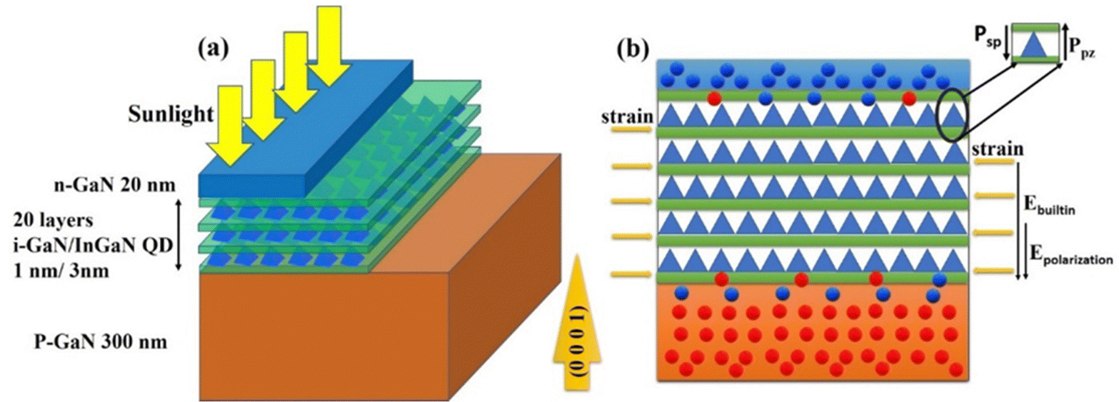 | ||
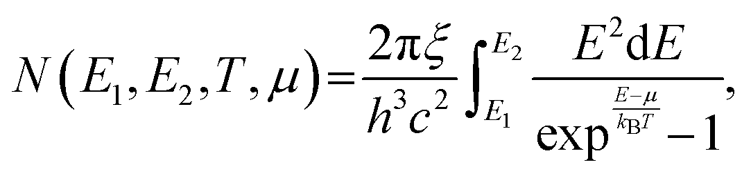
| Fig. 1 (a) Epitaxial layer structure of IBSC based on In0.5Ga0.5N QDs embedded in a GaN matrix with 1 nm GaN interlayers. (b) Schematic diagram of polarization-induced charges, and the electric fields at the In0.5Ga0.5N/GaN interfaces. The inset shows the directions of spontaneous polarization (Psp) and piezoelectric polarization (Ppz) at the interface. | ||
The wurtzite structure of InxGa1−xN gives rise to a pronounced polarization effect due to the non-centric symmetry of charges. This Epolarization polarization effect, along with potential barriers and band bending, significantly influences the behaviour of devices.47 The characteristics of InxGa1−xN alloy exhibit a nonlinear dependence on the alloy composition, resulting in complex properties.48 The wurtzite structure encompasses two types of polarization. The first type, known as Psp, is an inherent property of wurtzite semiconductors and arises from the absence of an inversion plane perpendicular to the c-axis.49 This phenomenon contributes to variations in dislocation density and surface morphology.46 Importantly, the Psp values for InN and GaN are nearly equal.49 The calculation of Psp can be determined using the following relation:50
| Psp(InxGa1−xN) = xPsp(InN) + (1 − x)Psp(GaN) − bInGax(1 − x) | (1) |
The presence of a second type of polarization, referred to as Ppz, can be observed in strained epitaxial layers. This polarization arises from the lattice-relaxation strain that occurs when two different materials are grown on the same substrate. In the case of wurtzite nitrides, the growth under biaxial strain induces piezoelectric polarization.50 The magnitude of Ppz depends on the composition of the InxGa1−xN alloy and is related to its binary constituents, InN and GaN, through the following relation:51
| Ppz(InxGa1−xN) = xPpz(InN) + (1 − x)Ppz(GaN) | (2) |
In our specific case, the growth of InN QDs on a GaN layer with lattice mismatch induces strain effects due to the relaxation of the mismatched layers. A 1 nm interlayer of i-GaN is incorporated to mitigate this strain. The total polarization (PT = Epolarization) is determined by the combined contributions of Ppz and Psp. Since the layers are in compression, the two polarizations act in opposite directions (as shown in the inset in Fig. 1(b)), resulting in a reduced net polarization. The presence of a built-in electric field and lower polarization field facilitates the movement of more carriers across the interfaces from the n-type to the p-type layer. Fig. 1(b) displays the calculated PT at the interfaces, along with the directions of the spontaneous polarization (Psp) and piezoelectric polarization (Ppz) at the interface. The structures demonstrate the lattice orientations and the corresponding vectors of Psp.52
The following list of assumptions is used to carry out limiting efficiency calculations.
1. The solar cell absorbs blackbody radiation at a temperature of Ts = 6000 K and ambient Ta = 300 K and emits blackbody radiation at ambient Ta = 300 K.
2. Only radiative transitions occur between the bands.
3. All photons above the lowest energy gap are absorbed, and no high-energy photon is used in a low-energy process.
4. Carrier mobility is infinite; consequently, the quasi-Fermi energy levels are constant throughout the cell.
5. Only one electron–hole pair is created per photon.
6. A perfect mirror is located on the back of the cell so that radiation makes a double pass and can only escape through the front illumination area.
7. The net photon flux (number of incident photons minus the number of emitted photons) equals the number of charge carrier pairs collected at the contacts.9
In the case of intermediate band solar cells (IBSCs), the detailed balance assumptions mentioned above are applied with slight modifications as follows:
Firstly, it is assumed that photons with photon energy Eph < Eg are absorbed, even though they fall below the energy bandgap. This is possible because an additional bandgap within the forbidden region has been introduced, which is isolated and has zero density of states. Secondly, the original bandgap Eg (Eg = E1 + E2) is split into two separate energy levels, E1 and E2. This splitting facilitates the absorption of photons with energy Eph < Eg. Therefore, in addition to absorbing photons with Eph ≥ Eg using the conventional mechanism, IBSCs can also absorb photons with Eph < Eg (assumption 3). As a result of absorbing photons with Eph < Eg, the absorptivity of the cell increases. However, it should be noted that only one additional electron–hole pair contributes to the short-circuit current density, Jsc (assumption 5). Moreover, the intermediate band (IB) is partially filled, and the valence band offset is considered to be negligible. It is important to mention that the output voltage is not calculated based on the IB (assumption 7).4
Taking the aforementioned factors into account, the electronic state of quantum dots (QDs) is determined by utilization of the Schrödinger equation, employing the Kronig–Penney model. Our previous work53 extensively discussed the theoretical framework behind this calculation. The position and width of the QDs are further optimized using the envelope function approximation. Simultaneously, the electronic properties are computed by solving Poisson's equation. To integrate these two calculations, we employ COMSOL Multiphysics, a software platform that combines the Schrödinger equation and electrostatics. This integration enables us to model the behavior of charge carriers in quantum-confined systems. Notably, the electric potential derived from the electrostatics is incorporated into the potential energy term of the Schrödinger equation within the COMSOL Multiphysics framework.
The solar cell and sun are considered blackbody systems. By applying the Roosbroeck–Shockley formula, the photon flux within the energy range of E1 to E2 can be determined using the following calculations,20
 | (3) |
| μ = EFC − EFV = 3.39 eV, μ1 = EFIB − EFV = 1.89 eV, μ2 = EFC − EFIB = 1.5 eV, | (4) |
 | (5) |
 | (6) |
 | (7) |
The efficiency (η) can be calculated as:
 | (8) |
Results and discussion
QDs are incorporated within the intrinsic absorber layer, and their position, width, and interdot size have been extensively studied for a 50% indium concentration. The structure of the simulated SC is depicted in Fig. 1(a), where the IB region is positioned between p-GaN and n-GaN materials. To minimize polarization effects within the IBSC's active layer, a Ga-face n–i–p structure is employed. The p-layer has a thickness of 300 nm, while the n-layer is 20 nm thick, and both layers have a doping concentration of 5 × 1018 cm−3. A thin cap layer reduces surface recombination from the n-layer, allowing maximum photon absorption in the device's active layer.37 The QDs are arranged in close proximity, both horizontally and vertically, enabling the penetration of wave functions from the QD region to the barrier region, effectively creating an intrinsic barrier within the forbidden region of the conventional bandgap.5 However, it is crucial to avoid inappropriate stacking of the QD layers, as this would result in QD localization within their designated region and prevent the formation of the intrinsic barrier. Therefore, careful placement and stacking of the QDs is necessary to establish the intrinsic barrier6 effectively. The QDs are selected with dimensions ranging from 1 to 5 nm, while the interdot distances vary from 1 to 3 nm.53 These 20 layers of QDs are grown on top of p-GaN. The growth of InxGa1−xN on GaN with sapphire substrates introduces in-plane strain. To limit the elastic energy stored in the InxGa1−xN layers, referred to as the critical thickness,55 an additional interlayer is introduced to alleviate the compressive strain on the In0.5Ga0.5N quantum dots.46 The presence of strained InxGa1−xN layers helps suppress phase separation.56Numerical experimentation has been conducted to simulate the QD-IBSC device and analyze the behavior of stacked quantum dot layers. The calculation of the band structure employs a tight-binding model that superimposes wave functions for the individual quantum dots. The finite element method technique is utilized to solve the model to enhance computational efficiency. The simulation process involves several steps. Firstly, the eigenvalues of the quantum dots are determined by solving the Schrödinger equation.53 Subsequently, the impact of embedding QDs in the intrinsic layer of a Ga-face n–i–p SC under the conditions mentioned above is simulated. The modeling incorporates the material properties specified in Table 1.
| Parameters | Values |
|---|---|
| Bandgap (Eg) | 1.6875 (eV) |
| Lifetime (τ) | 6.5 (ns) |
| Effective conduction band density of In0.5Ga0.5N | 1.6 × 10¹⁸ (cm−3) |
| Effective valence band density of In0.5Ga0.5N | 9 × 10¹⁸ (cm−3) |
| Effective electron mass of In0.5Ga0.5N | 0.16 m0 |
| Effective hole mass of In0.5Ga0.5N | 0.585 m0 |
| Electron affinity | 5.29875 (eV) |
| Elastic constant (c13) | 100 (GPa) |
| Elastic constant (c33) | 299 (GPa) |
| Piezoelectric Const. (e31) | 0.04 (C m−2) |
| Piezoelectric Const. (e31) | 0.88 (C m−2) |
Optical modes and the distribution of the electric field are also considered. The Fresnel model is applied to optimize the reflection and transmission of light. Boundaries are fine-tuned using Floquet's periodicity condition. Moreover, the influence of thin enough material strain is considered as per the equation described in Section 2 of the referenced article.
The three-dimensional doping profile of the proposed structure with excited state energy is shown in Fig. 2(a). The blue color shows the concentration of excess electrons, whereas the red indicates the excess holes. The green color indicates the intrinsic level with no doping. The inset shows the excited state energies of the QDs. Fig. 2(b) shows the energy band diagram for the proposed structure. Ec and Ev are the CB and VB energy levels, respectively. EIB is the IB energy level created when QDs are placed within the intrinsic level of n–i–p IBSC. These bands have their Fermi levels. Efc and Efv are the quasi-Fermi levels for the CB and VB. The intermediate band has its Fermi level EfIB which is separated from the quasi-Fermi levels of the CB and VB. This IB is half-filled with electrons by optimizing the distance between QDs and spacing between barrier regions.53Eg is the bandgap of GaN (3.39 eV) and EInN is the bandgap for InN (0.7 eV). E1 and E2 are the energy gaps between Ev and EIB, EIB and EC, respectively. Lqd is the distance between two adjacent QDs, and Lbr is the width of the barrier. Upon illumination, photons are absorbed; if Eph (energy from photons) ≤ Eg, this energy photon is absorbed and creates an electron–hole pair. Additional electron–hole pairs are created other than the conventional ones, which results in higher efficiency.53 Additionally, low-energy photons below Eg are absorbed, thus increasing the photocurrent.
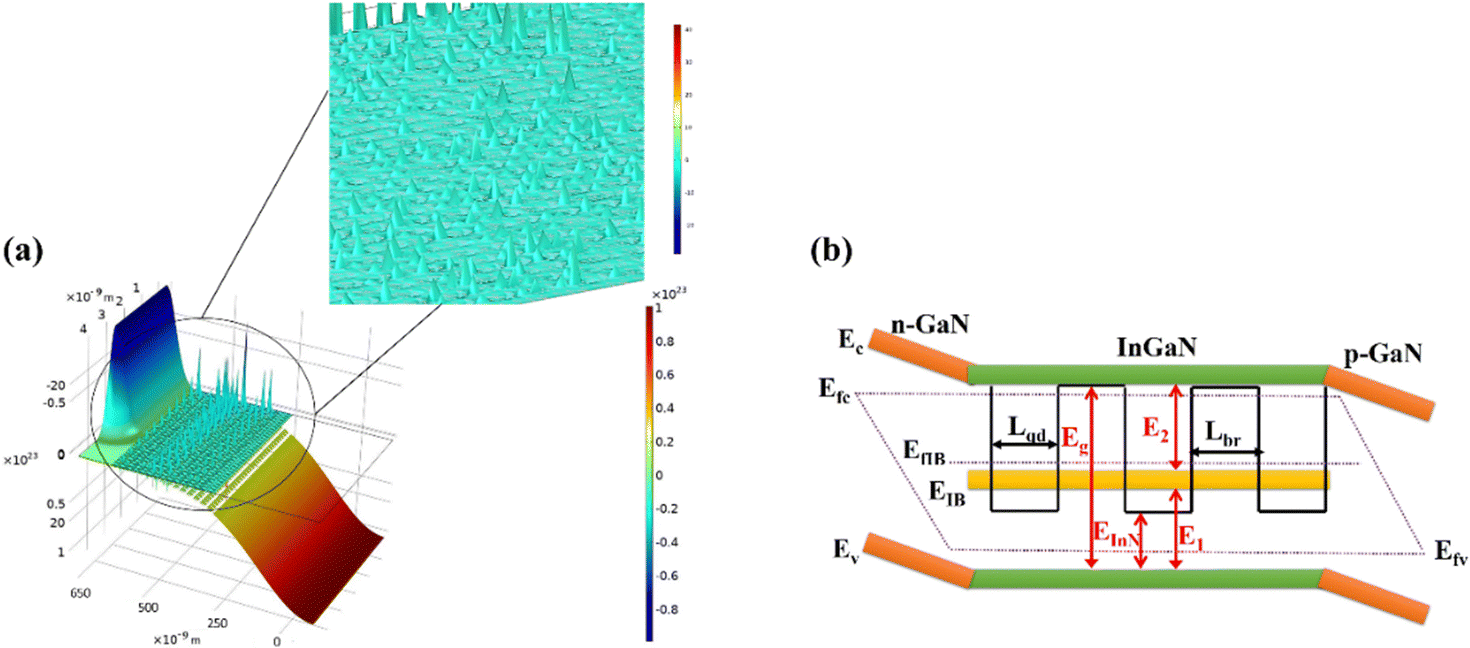 | ||
| Fig. 2 (a) Three-dimensional doping profile of the proposed device structure; the inset shows the ground state energy of the QD wave function. (b) Band structure of QD-IBSC, showing transitions from VB to IB (E1) and IB to CB (E2), their Fermi levels (EfIB, EfV and EfC) and energy gaps (Eg and EInN). | ||
Fig. 3(a)–(c) shows the 3 × 3 layer of QDs with their localized wave functions for the QD size of 3 nm and their interdot distance of 2 nm. Three eigenvalues are inside the conduction band at 1.3479, 1.8472, and 2.6289 eV. The first state is the pure quantum dot state. The wave function for this state is zero at the center of the quantum dot and vanishes at the boundary. The second and third states are weakly confined concerning the first state.57 The band formation of IB strongly depends on the dot sizes53 and interdot spacing between each QD. The wave functions of the QDs will overlap for certain QD sizes and interdot spacings such that energy level splitting occurs. Small confinement in barriers increases the tunneling probability of the wavefunctions.53 Due to the quantum confinement effect, QD coupling occurs as soon as they are brought near each other. This results in new band formation within the available density of states (Fig. 4). The colors in Fig. 3 show the QD states for the excited states.
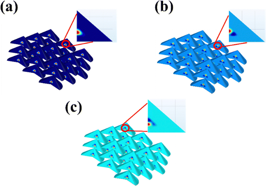 | ||
| Fig. 3 WF of a system: (a) ground state E0 = 1.34 eV, (b) first excited state E1 = 1.85 eV and (c) second excited state E2 = 2.63 eV. | ||
 | ||
| Fig. 4 Variation of the first optically strongest four states in the conduction band interdot spacing. | ||
As identical quantum dots (QDs) are brought together, they form a QD array where their wave functions become highly extended, and their energy level becomes very small. Consequently, the energy bands formed by the QDs exhibit continuity rather than discrete levels,27 as shown in Fig. 4. This can be explained using the QD Bloch state, i.e., eikz, where the QD wavenumber ‘k’ lies between −π/L to π/L where L is the measure of one period (Lqd + Lbr). Within this range, certain energy intervals between the intrinsic barriers (IBs) are unoccupied by the QD energies, resulting in energy gaps. These gaps represent regions with zero density of states, where carriers cannot thermally depopulate from the conduction band (CB) to the intrinsic barrier due to the delocalization of wave functions in the ground state energy.11Fig. 4 particularly estimates the variation in miniband formation for interdot spacing and size of the QD. The width of the E0 miniband at Lqd = 1 nm is 403.6 eV; at Lqd = 3 nm it is 60.9 eV and it is lowered as the QD size decreases or the distance between vertically stacked QDs increases. For small QD sizes, the E1, E2 and E3 are so close that they overlap with the CB edge of the barrier material. Increasing the QD size decreases the gap between the ground states of the hole and electrons (IB-VB).
The inclusion of thin interlayers is crucial for absorbing excess indium and relieving compressive strain. These GaN interlayers need to strike a balance between being thick enough to be effective and thin enough to facilitate carrier transport through tunneling. The In0.5Ga0.5N QD layers should be thick enough to capture the incident light beam while remaining fully strained. Fig. 5(a) exhibits increasing interlayer effects on the electrical parameters of QD-IBSC. Critical thickness plays a very vital role in strain layers. The barrier height at higher indium concentrations causes current transport through tunneling. The tunneling current diminishes even when the barrier thickness remains constant. The thickness of the GaN interlayer decreases the power conversion efficiency, as shown in Fig. 5(b).
 | ||
| Fig. 5 (a) J–V characteristics and (b) efficiency of In0.5Ga0.5N/GaN QD-IBSC as a function of interlayers with QD layer = 20, Lqd = 3 nm, and Lbr = 3 nm, respectively. | ||
Fig. 6(a) depicts the relationship between the Jsc and η as a function of the number of QD layers. It is observed that the increasing slope of Jsc reaches a maximum value of 34.2 mA cm−2, while the efficiency peaks at 20 layers. Additionally, the Voc also experiences an increase in the proposed structure. During illumination, a significant number of photons are absorbed in the top n-layer. Due to the higher mobility of electrons compared to holes, the electrons are transported from the n-layer to the p-layer. The energy band bending depends on the interfaces and the electric field induced within the materials, specifically, GaN and In0.5Ga0.5N. The total induced polarization (Epolarization), as discussed in the device theory section, is reduced. Moreover, the built-in electric field (Ebuiltin) aligns in the same direction, facilitating the movement of carrier charges from the n-layer to the p-layer. This phenomenon contributes to the increased efficiency depicted in Fig. 6(b). Therefore, it can be concluded that the optimized configuration for maximum efficiency consists of up to 20 layers according to the proposed structure. It is worth noting that the literature suggests that increasing the number of QD layers introduces strain.5,38–40 However, the inclusion of i-GaN interlayers absorbs the strain generated at the interfaces, leading to an enhancement in both Jsc and η.
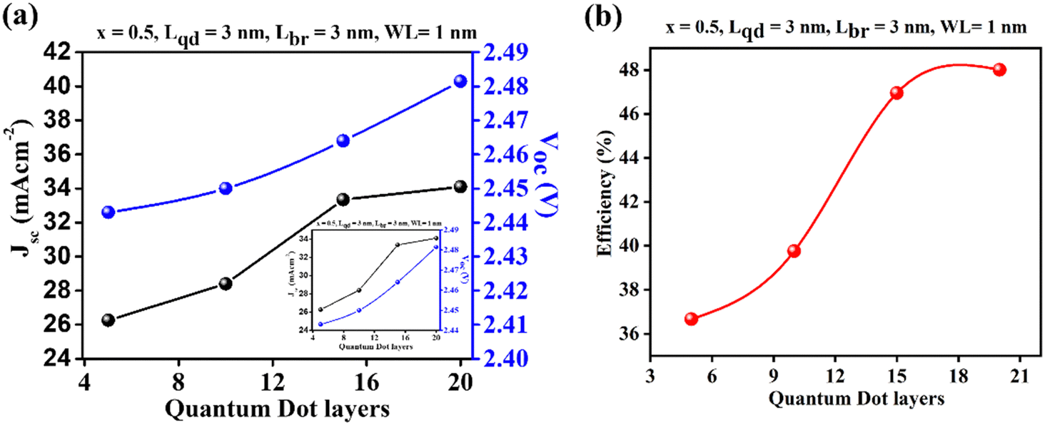 | ||
| Fig. 6 (a) J–V characteristics and (b) efficiency of In0.5Ga0.5N/GaN QD-IBSC as a function of QD layers with Lqd = 3 nm, Lbr = 3 nm, respectively. | ||
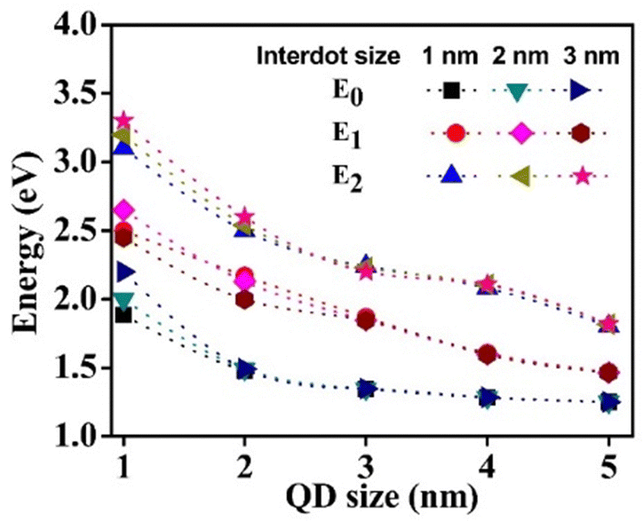
Fig. 7(a) and (b) provide insights into the J–V characteristics and efficiency of the QD-IBSC with respect to different parameters. It is observed that both the J–V characteristics and efficiency show an increasing trend as the QD size increases. The maximum efficiency achieved is 45% under the conditions of Lbr = 3 nm, Lqd = 3 nm, and x = 0.5. For smaller QD sizes, the IB widens, leading to an increased carrier concentration and current. The Voc remains constant for two values, then increases, and becomes constant again. The size of the quantum dot significantly influences the performance of the QD-IBSC. Larger QD sizes result in a lower position of the IB, allowing more space for accumulating bands and the creation of additional IBs. However, there is a limit to the number of IBs that can be formed. In this particular device, three bands are created within the forbidden region, leading to the generation of additional electron–hole pairs and enhancing the device's efficiency. In Fig. 7(c), it is demonstrated that the energy is maximum for the smallest QD size. The wave functions of the electrons are localized within the QDs, and the quantum confinement effect causes discrete energy levels rather than continuous energy levels. The sub gap decreases as the QD size increases due to this quantum confinement effect within the QDs.
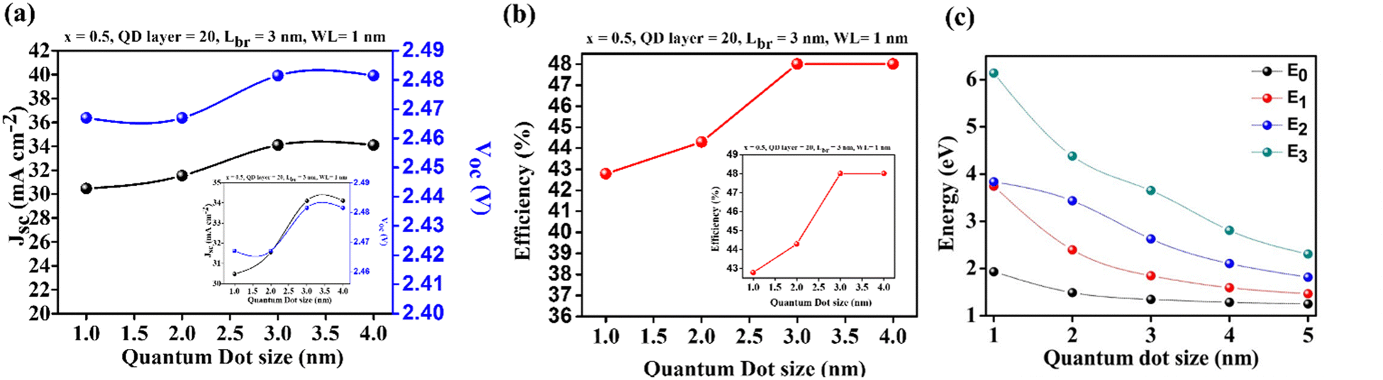 | ||
| Fig. 7 (a) J–V characteristics, (b) efficiency and (c) excited state energies of In0.5Ga0.5N/GaN QD-IBSC as a function of QD size and IB formation in the CB for x = 0.5, QD layers = 20, Lbr = 3 nm and WL = 1 nm. | ||
Fig. 8(a) shows that an increase in the interdot size leads to a decrease in the Jsc. This reduction is attributed to the localization of QDs as the Lbr increases. The weaker coupling of the wave functions results in individual QD behaviour, rather than a collective band behaviour. Additionally, the interdot size influences the width of the IB. Larger interdot sizes lead to higher sub-bandgap transition energies,53 resulting in lower overall efficiency. Fig. 8(b) illustrates the optimum efficiency of 49% obtained with specific parameters: Lqd of 3 nm, Lbr of 1 nm, and x of 0.5. It shows a decrease in efficiency, which drops abruptly and significantly affects the performance of the QD-IBSC. This decrease is primarily attributed to recombination rates, especially radiative recombination, becoming dominant for small interdot distances. The reduction in bandgap at an indium composition of 0.5 contributes to this effect. On the other hand, Fig. 8(c) demonstrates the relationship between interdot distance and energy. When QDs are stacked at specific distances and sizes, wave function delocalization occurs, forming an IB. The interdot distance variation affects the bandwidth of the IBs, where larger interdot distances result in narrower bandwidths and discrete energy levels. A summary of this work is presented in Table 2.
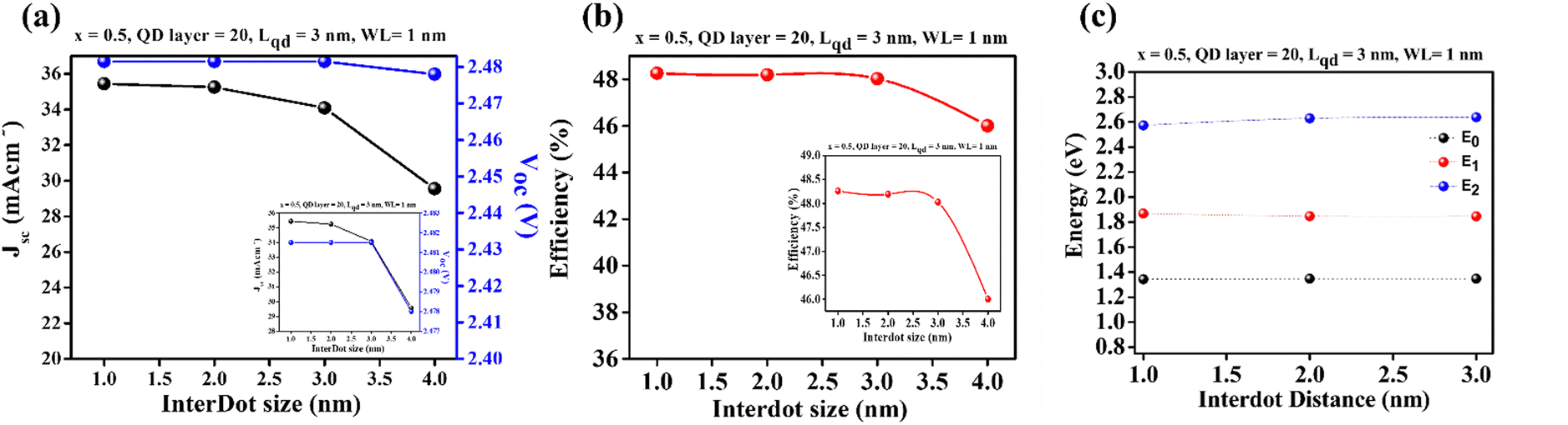 | ||
| Fig. 8 (a) J–V characteristics, (b) efficiency and (c) E0, E1, E2 of In0.5Ga0.5N/GaN QD-IBSC as a function of distance between two QDs for x = 0.5, QD layers = 20, Lqd = 3 nm and WL = 1 nm. | ||
| Concentration | QD layer | QD size (nm) | Interdot (nm) | J sc (mA cm−2) | V oc (V) | FF (%) | η (%) |
|---|---|---|---|---|---|---|---|
| 0.5 | 5 | 3 | 3 | 20.27 | 2.44 | 74.39 | 36.669 |
| 10 | 28.4 | 2.45 | 57.14 | 39.76 | |||
| 15 | 33.35 | 2.464 | 60.79 | 46.95 | |||
| 20 | 34.1 | 2.451 | 57.5 | 48.01 |
Conclusion
In this paper, we proposed an optical structure that could increase photoelectric efficiency by applying and optimizing i-GaN layers in the active layer. The applied 1 nm thick i-GaN layer could compensate for the lattice mismatch caused by the In0.5Ga0.5N QD/GaN layer and absorb the excess strain to increase efficiency. We investigated the optical effect of the i-GaN interlayer by calculating the optical properties of Ga-face n–i–p QD-IBSCs in In0.5Ga0.5N/GaN arrays containing the i-GaN interlayer in the active layer under illumination. In our calculations, we applied 20 stacked high-concentration indium QD layers (In0.5Ga0.5N) that consist of 3 nm of QD size, 3 nm of an inter-dot size and 1 nm of a GaN layer (Eg = 1.6875 eV,) respectively. As a result, the photovoltaic efficiency of the device InxGa1−xN QD-IBSCs with an interlayer structure could potentially reach 48%. The optimal quantum dot structure size, interlayer thickness, and interdot spacing must be meticulously considered in the fabrication of QD-IBSCs using molecular beam epitaxy. This study is anticipated to provide solutions to the challenges encountered in the experimental fabrication of InxGa1−xN QD-IBSCs.Author contributions
D. E. conceptualized the theoretical framework, simulated the device and wrote the manuscript. J. J. supervised and edited the manuscript. A. I. helped in simulation, and investigation of the device. A. A. K. revised the manuscript and helped in writing, and editing the visualizations.Conflicts of interest
There are no conflicts to declare.Acknowledgements
This work was supported by the National Key R&D Program of China [grant number 2017YFB0405100].References
- M. A. Green, E. D. Dunlop, J. Hohl-Ebinger, M. Yoshita, N. Kopidakis and X. Hao, Solar cell efficiency tables (Version 58), Prog. Photovoltaics, 2021, 29(7), 657–667 Search PubMed.
- A. Jäger-Waldau, Snapshot of photovoltaics–February 2022, EPJ Photovoltaics, 2022, 13, 9 CrossRef.
- V. Benda and L. Černá, PV cells and modules – State of the art, limits and trends, Heliyon, 2020, 6(12), e05666 CrossRef.
- A. Luque and A. Martí, Increasing the efficiency of ideal solar cells by photon induced transitions at intermediate levels, Phys. Rev. Lett., 1997, 78(26), 5014 CrossRef CAS.
- A. Luque, A. Martí and C. Stanley, Understanding intermediate-band solar cells, Nat. Photonics, 2012, 6(3), 146–152 CrossRef CAS.
- A. Luque and A. Marti, A metallic intermediate band high efficiency solar cell, Prog. Photovoltaics Res. Appl., 2001, 9(2), 73–86 CrossRef CAS.
- M. Wolf, Limitations and Possibilities for Improvement of Photovoltaic Solar Energy Converters: Part I: Considerations for Earth's Surface Operation, Proc. IRE, 1960, 48(7), 1246–1263 Search PubMed.
- T. Sogabe, C.-Y. Hung, R. Tamaki, S. Tomić, K. Yamaguchi, N. Ekins-Daukes and Y. Okada, Experimental demonstration of energy-transfer ratchet intermediate-band solar cell, Commun. Phys., 2021, 4(1), 38 CrossRef.
- W. Shockley and H. J. Queisser, Detailed Balance Limit of Efficiency of p–n Junction Solar Cells, J. Appl. Phys., 1961, 32(3), 510–519 CrossRef CAS.
- S. Wang, X. Yang, H. Chai, Z. Lv, S. Wang, H. Wang, H. Wang, L. Meng and T. Yang, Detailed Balance-Limiting Efficiency of Solar Cells with Dual Intermediate Bands Based on InAs/InGaAs Quantum Dots, Photonics, 2022, 9(5), 290 CrossRef CAS.
- A. B. E. Cristóbal, L. O. A. Martí and V. A. L. López, Next Generation of Photovoltaics-New Concepts, Springer, 2012, pp. 229–250 Search PubMed.
- A. Luque, A. Mellor, I. Ramiro, E. Antolín, I. Tobías and A. Martí, Interband absorption of photons by extended states in intermediate band solar cells, Sol. Energy Mater. Sol. Cells, 2013, 115, 138–144 CrossRef CAS.
- A. Imran, J. Jiang, D. Eric, M. N. Zahid, M. Yousaf, M. Ahmad and S. A. Hassan, Efficiency enhancement through flat intermediate band in Quantum dot solar cell, Results Phys., 2018, 10, 241–247 CrossRef.
- A. A. Khan, Z. Yu, U. Khan and L. Dong, Solution Processed Trilayer Structure for High-Performance Perovskite Photodetector, Nanoscale Res. Lett., 2018, 13(1), 399 CrossRef PubMed.
- M. F. Iqbal, K. Ullah, M. M. Yaqoob, A. A. Khan, S. Farid, P. Zhu and D. Wang, Anharmonic phonon coupling and decay of optical phonons in polycrystalline CdSe thin films, Ceram. Int., 2022, 48(16), 23862–23869 CrossRef CAS.
- L. Cuadra, A. Martí and A. Luque, Present status of intermediate band solar cell research, Thin Solid Films, 2004, 451–452, 593–599 CrossRef CAS.
- A. Luque, A. Martí and L. Cuadra, In High efficiency solar cell with metallic intermediate band, Proc. of the 16th European Photovoltaic Solar Energy Conference, 2000, pp. 59–61.
- B. Stefan, Modeling of semiconductor nanostructures and semiconductor–electrolyte interfaces, 2011 Search PubMed.
- X. Wang, B. Li, L. Dong, Y. S. Yi, M. Yousaf, D. Eric, J. Jiang and A. Imran, Size and shape dependent optical properties of InAs quantum dots, 2018, p. 11.
- X. Wang, B. Li, L. Dong, Y. S. Yi, M. Yousaf, D. Eric, J. Jiang and A. Imran, Numerical modelling of high efficiency InAs/GaAs intermediate band solar cell, 2018, p. 17.
- M. Zhang, X. Ma, H. Zhang, L. Zhu, L. Xu, F. Zhang, C.-S. Tsang, L. Y. S. Lee, H. Y. Woo, Z. He and W.-Y. Wong, Metallated terpolymer donors with strongly absorbing iridium complex enables polymer solar cells with 16.71% efficiency, Chem. Eng. J., 2022, 430, 132832 CrossRef CAS.
- S. Zhang, M. Zhang, X. Wang, C. Xu, W. Xu, J. Gao, J. Wang, W.-Y. Wong, J. H. Son, S. Y. Jeong, H. Y. Woo and F. Zhang, Ternary polymer solar cells with iridium-based polymer PM6Ir1 as a donor and N3:ITIC-Th as an acceptor exhibiting over 17.2% efficiency. Sustainable, Energy Fuels, 2021, 5(22), 5825–5832 CAS.
- Z. Zheng, H. Ji, P. Yu and Z. Wang, Recent Progress Towards Quantum Dot Solar Cells with Enhanced Optical Absorption, Nanoscale Res. Lett., 2016, 11(1), 266 CrossRef.
- I. Ramiro, E. Antolin, J. Hwang, A. Teran, A. J. Martin, P. G. Linares, J. Millunchick, J. Phillips, A. Marti and A. Luque, Three-Bandgap Absolute Quantum Efficiency in GaSb/GaAs Quantum Dot Intermediate Band Solar Cells, IEEE J. Photovolt., 2017, 7(2), 508–512 Search PubMed.
- A. A. Khan, M. Azam, D. Eric, G. Liang and Z. Yu, Triple cation perovskite doped with the small molecule F4TCNQ for highly efficient stable photodetectors, J. Mater. Chem. C, 2020, 8(8), 2880–2887 RSC.
- M. M. Wilkins, E. C. Dumitrescu and J. J. Krich, Material Quality Requirements for Intermediate Band Solar Cells, IEEE J. Photovolt., 2020, 10(2), 467–474 Search PubMed.
- Y. Okada, N. J. Ekins-Daukes, T. Kita, R. Tamaki, M. Yoshida, A. Pusch, O. Hess, C. C. Phillips, D. J. Farrell, K. Yoshida, N. Ahsan, Y. Shoji, T. Sogabe and J. F. Guillemoles, Intermediate band solar cells: Recent progress and future directions, Appl. Phys. Rev., 2015, 2(2), 021302 Search PubMed.
- S. Strite, GaN, AlN, and InN: A review, J. Vac. Sci. Technol., B: Microelectron. Nanometer Struct.--Process., Meas., Phenom., 1992, 10(4), 1237 CrossRef CAS.
- I. Vurgaftman, J. R. Meyer and L. R. Ram-Mohan, Band parameters for III–V compound semiconductors and their alloys, J. Appl. Phys., 2001, 89(11), 5815–5875 CrossRef CAS.
- C. M. Duque, M. E. Mora-Ramos and C. A. Duque, Exciton properties in zinc blende InGaN–GaN quantum wells under the effects of intense laser fields, Nanoscale Res. Lett., 2012, 7(1), 492 CrossRef.
- C.-X. Xia, J.-J. Shi and S.-Y. Wei, Exciton States in Wurtzite InGaN Coupled Quantum Dots, Chin. Phys. Lett., 2004, 21(8), 1620 CrossRef CAS.
- C. Xia, Z. Zeng, Q. Chang and S. Wei, Donor impurity states in zinc blende InGaN/GaN asymmetric coupled quantum dots: Hydrostatic pressure effect, Phys. E, 2010, 42(8), 2041–2046 CrossRef CAS.
- D. V. P. McLaughlin and J. M. Pearce, Analytical model for the optical functions of indium gallium nitride with application to thin film solar photovoltaic cells, Mater. Sci. Eng., B, 2012, 177(2), 239–244 CrossRef CAS.
- Y. C. Lin, S. J. C. Y. K. Su, T. Y. Tsai, C. S. Chang, S. C. Shei, C. W. Kuo and S. C. Chen, InGaN/GaN light emitting diodes with Ni/Au, Ni/ITO and ITO p-type contacts, Solid-State Electron., 2003, 47, 849–853 CrossRef.
- A. E. Aouami, L. M. Pérez, K. Feddi, M. El-Yadri, F. Dujardin, M. J. Suazo, D. Laroze, M. Courel and E. M. Feddi, Influence of Geometrical Shape on the Characteristics of the Multiple InN/InxGa1−xN Quantum Dot Solar Cells, Nanomaterials, 2021, 11(5), 1317 CrossRef.
- L. M. Pérez, A. E. Aouami, K. Feddi, V. Tasco, A. B. Abdellah, F. Dujardin, M. Courel, J. A. Riquelme, D. Laroze and E. M. Feddi, Parameters Optimization of Intermediate Band Solar Cells: Cases of PbTe/CdTe, PbSe/ZnTe and InN/GaN Quantum Dots, Crystals, 2022, 12(7), 1002 CrossRef.
- A. Aissat, F. Benyettou and J. P. Vilcot, Modeling and simulation of InGaN/GaN quantum dots solar cell, AIP Conf. Proc., 2016, 1758, 030014 CrossRef.
- K.-F. Chen, C.-L. Hung and Y.-L. Tsai, Simulation study of InGaN intermediate-band solar cells, J. Phys. D: Appl. Phys., 2016, 49(48), 485102 CrossRef.
- Q.-W. Deng, X.-L. Wang, C.-B. Yang, H.-L. Xiao, C.-M. Wang, H.-B. Yin, Q.-F. Hou, Y. Bi, J.-M. Li, Z.-G. Wang and X. Hou, Computational Investigation of InxGa1−xN/InN Quantum-Dot Intermediate-Band Solar Cell, Chin. Phys. Lett., 2011, 28(1), 018401 CrossRef.
- Q. Zhang and W. Wei, Single intermediate-band solar cells of InGaN/InN quantum dot supracrystals, Appl. Phys. A: Mater. Sci. Process., 2013, 113(1), 75–82 CrossRef CAS.
- J. Dickerson, K. Pantzas, T. Moudakir, A. Ougazzaden and P. L. Voss, Modeling of polarization effects on n-GaN/i-InGaN/p-Gan solar cells with ultrathin GaN interlayers, Opt. Quantum Electron., 2013, 45(7), 681–686 CrossRef CAS.
- S. A. Kazazis, E. Papadomanolaki and E. Iliopoulos, Polarization-Engineered InGaN/GaN Solar Cells: Realistic Expectations for Single Heterojunctions, IEEE J. Photovolt., 2018, 8(1), 118–124 Search PubMed.
- K. Wang, Q. Wang, J. Chu, H. Xiao, X. Wang and Z. Wang, Roles of polarization effects in InGaN/GaN solar cells and comparison of p–i–n and n–i–p structures, Opt. Express, 2018, 26(22), A946–A954 CrossRef CAS PubMed.
- F. Zhang, M. Ikeda, R. Zhou, J. Liu, S. Zhang, A. Tian, P. Wen, D. Li, L. Zhang and H. Yang, Polarization relaxation in InGaN/(In)GaN multiple quantum wells, Jpn. J. Appl. Phys., 2019, 58(SC), SCCB12 CrossRef CAS.
- A. Jiang, S. Xing, H. Lin, Q. Chen and M. Li, Role of Pyramidal Low-Dimensional Semiconductors in Advancing the Field of Optoelectronics, Photonics, 2024, 11(4), 370 CrossRef CAS.
- J. R. Dickerson, K. Pantzas, A. Ougazzaden and P. L. Voss, Polarization-Induced Electric Fields Make Robust n-GaN/i-InGaN/p-GaN Solar Cells, IEEE Electron Device Lett., 2013, 34(3), 363–365 CAS.
- O. Ambacher, J. Smart, J. R. Shealy, N. G. Weimann, K. Chu, M. Murphy, W. J. Schaff, L. F. Eastman, R. Dimitrov, L. Wittmer, M. Stutzmann, W. Rieger and J. Hilsenbeck, Two-dimensional electron gases induced by spontaneous and piezoelectric polarization charges in N- and Ga-face AlGaN/GaN heterostructures, J. Appl. Phys., 1999, 85(6), 3222–3233 CrossRef CAS.
- R. F. W. Bader, Dielectric polarization: a problem in the physics of an open system, Mol. Phys., 2002, 100(21), 3333–3344 CrossRef CAS.
- M. Feneberg and K. Thonke, Polarization fields of III-nitrides grown in different crystal orientations, J. Phys.: Condens. Matter, 2007, 19(40), 403201 CrossRef CAS PubMed.
- R. Kour, S. Arya, S. Verma, A. Singh, P. Mahajan and A. Khosla, Review—Recent Advances and Challenges in Indium Gallium Nitride (InxGa1−xN) Materials for Solid State Lighting, ECS J. Solid State Sci. Technol., 2020, 9(1), 015011 CrossRef CAS.
- F. Bernardini and V. Fiorentini, Nonlinear macroscopic polarization in III-V nitride alloys, Phys. Rev. B: Condens. Matter Mater. Phys., 2001, 64(8), 085207 CrossRef.
- H. Ray-Hua, L. Shih-Ting, T. Yu-Li, C. Mu-Tao, L. Wen-Yih, W. Ming-Hsien, L. Ray-Ming and L. Yuan-Chieh, Improved Conversion Efficiency of GaN/InGaN Thin-Film Solar Cells, IEEE Electron Device Lett., 2009, 30(7), 724–726 Search PubMed.
- D. Eric, J. Jiang, A. Imran, M. Noaman Zahid and A. Ahmad Khan, Optical properties of InN/GaN quantum dot superlattice by changing dot size and interdot spacing, Results Phys., 2019, 13, 102246 CrossRef.
- A. Imran, J. Jiang, D. Eric, M. N. Zahid, M. Yousaf and Z. H. Shah, Optical properties of InAs/GaAs quantum dot superlattice structures, Results Phys., 2018, 9, 297–302 CrossRef.
- I.-H. Kim, H.-S. Park, Y.-J. Park and T. Kim, Formation of V-shaped pits in InGaN/GaN multiquantum wells and bulk InGaN films, Appl. Phys. Lett., 1998, 73(12), 1634–1636 CrossRef CAS.
- S. Y. Karpov, Suppression of phase separation in InGaN due to elastic strain, MRS Internet J. Nitride Semicond. Res., 1998, 3(1), 16 CrossRef.
- R. V. N. Melnik and M. Willatzen, Bandstructures of conical quantum dots with wetting layers, Nanotechnology, 2003, 15(1), 1–8 CrossRef.
| This journal is © The Royal Society of Chemistry 2024 |