
 Open Access Article
 This Open Access Article is licensed under a
 Creative Commons Attribution 3.0 Unported Licence
Vapor phase deposition of perovskite photovoltaics: short track to commercialization?†
Tobias
Abzieher
 *a,
David T.
Moore
*a,
Marcel
Roß
b,
Steve
Albrecht
b,
Jared
Silvia
c,
Hairen
Tan
d,
Quentin
Jeangros
e,
Christophe
Ballif
ef,
Maximilian T.
Hoerantner
g,
Beom-Soo
Kim
h,
Henk J.
Bolink
i,
Paul
Pistor
jk,
Jan Christoph
Goldschmidt
l,
Yu-Hsien
Chiang
mn,
Samuel D.
Stranks
mn,
Juliane
Borchert
op,
Michael D.
McGehee
q,
Monica
Morales-Masis
r,
Jay B.
Patel
s,
Annalisa
Bruno
t and
Ulrich W.
Paetzold
*u
*a,
David T.
Moore
*a,
Marcel
Roß
b,
Steve
Albrecht
b,
Jared
Silvia
c,
Hairen
Tan
d,
Quentin
Jeangros
e,
Christophe
Ballif
ef,
Maximilian T.
Hoerantner
g,
Beom-Soo
Kim
h,
Henk J.
Bolink
i,
Paul
Pistor
jk,
Jan Christoph
Goldschmidt
l,
Yu-Hsien
Chiang
mn,
Samuel D.
Stranks
mn,
Juliane
Borchert
op,
Michael D.
McGehee
q,
Monica
Morales-Masis
r,
Jay B.
Patel
s,
Annalisa
Bruno
t and
Ulrich W.
Paetzold
*u
aNational Renewable Energy Laboratory (NREL), Golden, CO, USA. E-mail: tobias.abzieher@gmail.com; david.moore@nrel.gov
bHelmholtz Zentrum Berlin (HZB), Berlin, Germany
cBlueDot Photonics Inc, Seattle, WA, USA
dNanjing University, Nanjing, China
eCentre Suisse d’Electronique et de Microtechnique (CSEM), Neuchâtel, Switzerland
fÉcole Polytechnique Fédérale de Lausanne (EPFL), Institute of Electrical and Micro Engineering (IEM), Photovoltaics and Thin-Film Electronics Laboratory, Neuchâtel, Switzerland
gSwift Solar, San Carlos, CA, USA
hKorea Research Institute of Chemical Technology (KRICT), Daejeon, Republic of Korea
iUniversitat de València, València, Spain
jMartin-Luther-University Halle-Wittenberg, Halle, Germany
kUniversidad Pablo de Olavide (UPO), Seville, Spain
lPhilipps-University Marburg, Marburg, Germany
mDepartment of Chemical Engineering and Biotechnology, University of Cambridge, Cambridge, UK
nDepartment of Physics, University of Cambridge, Cambridge, UK
oFraunhofer Institute for Solar Energy Systems, Freiburg, Germany
pUniversity of Freiburg, INATECH, Freiburg, Germany
qUniversity of Colorado Boulder, Boulder, CO, USA
rMESA+ Institute for Nanotechnology, University of Twente, Enschede, The Netherlands
sDepartment of Physics, King's College London, London, UK
tNanyang Technological University, Singapore, Singapore
uKarlsruhe Institute of Technology (KIT), Karlsruhe, Germany. E-mail: ulrich.paetzold@kit.edu
First published on 23rd January 2024
Abstract
While perovskite-based photovoltaics (PV) is progressing toward commercialization, it remains an open question which fabrication technology – solution-based, vapor-based, or combinations – will pave the way to faster economic breakthrough. The vast majority of research studies make use of solution-processed perovskite thin films, which benefit from a rapid optimization feedback and inexpensive to procure tools in modern research laboratories, but vapor phase deposition processes dominate today's established thin-film manufacturing. As research and development of vapor phase processed perovskite thin films are still strongly underrepresented in literature, their full potential is yet to be identified. In this collaborative perspective of academic influenced by industrial views, we convey a balanced viewpoint on the prospects of vapor-based processing of perovskite PV at an industrial scale. Our perspective highlights the conceptual advantages of vapor phase deposition, discusses the most crucial process parameters in a technology assessment, contains an overview about relevant global industry clusters, and provides an outlook on the commercialization perspectives of the perovskite technology in general.
Broader contextWorldwide, perovskite PV is progressing rapidly toward commercialization, with the first solar module manufacturers expected to enter the market by 2024/2025. Despite this rapid progress, it is yet unknown which fabrication technology – solution-based, vapour-based, or combinations – will eventually pave the way toward the economic breakthrough at the terawatts scale. Although vapor phase deposition processes dominate today's established thin-film manufacturing, this processing route is heavily underrepresented in the majority of research studies on perovskite photovoltaics that employ solution-processed perovskite thin films. For this reason, the authors of this perspective feel urged to reach out to the community with our perspective on vapour phase deposition of perovskite PV. |
Introduction
Photovoltaics (PV) is one of the cornerstones for a resilient and sustainable energy supply in the 21st century and at the same time an integral element of the solution for the most pressing challenge of mankind: global climate change. At this juncture, photovoltaic energy conversion vastly relies on mono-crystalline silicon-based PV. While ongoing technological improvements of silicon-based PV will steadily decrease their costs, significant leaps ahead in cost reduction and performance are unlikely as the technology approaches its practical as well as theoretical limit in power conversion efficiency (PCE). Among the various candidates for next-generation PV technologies, organic–inorganic hybrid perovskite thin-film PV have positioned themselves a front runner in less than 15 years of development, achieving PCEs of 26% for single-junction solar cells and PCEs approaching 34% for multi-junction solar cells, already outpacing well established and longer researched PV technologies including organic photovoltaics (OPV, PCE up to 19.2%), cadmium telluride (CdTe, PCE up to 22.3%), copper indium gallium diselenide (CIGS, PCE up to 23.6%), and even multi-crystalline silicon solar cells (PCE up to 23.3%).1 This tremendous improvement within an unprecedented short development period is based on excellent optoelectronic material properties – including high absorption coefficients,2 high initial defect tolerance,3 high charge carrier mobility and long lifetimes,4–6 as well as tunability of its bandgap.7 Moreover, on a laboratory scale significant advances are demonstrated with regard to the weak spots of perovskite-based PV, such as the yet unproven durability of perovskite semiconductors thin films under operational conditions as well as understanding how to safely manufacture and deploy their potentially hazardous materials (mostly related to the use of lead and commonly employed solvents).8–11 To date, perovskite-based PV seems at the edge of commercialization, as evidenced by the considerable number of start-up companies as well as the wide interest in the technology from established PV manufacturers, equipment suppliers, and materials companies (see Discussion below). Nevertheless, it remains an open question if the technology will also be successful in the highly competitive PV mass market and which fabrication technology – solution-based, vapor-based, or combinations – will pave the way to faster economic breakthrough for the various perovskite-based PV technologies, e.g., perovskite-based single- and multi-junction PV, or light-weight and flexible perovskite PV.High-quality perovskite semiconductors are commonly processed via two distinct routes: solution-based or vapor-based approaches. Solution-based approaches apply inks that contain the precursor materials and suitable solvent systems that are spin-coated,12–14 blade-coated,15–17 slot-die-coated,18–20 spray-coated,21–23 or inkjet-printed on a substrate.24–26 In contrast, vapor-based processing employs dry and solvent-free methods that transfer the precursor materials into their vapor state by evaporating or subliming them under vacuum conditions, following a condensation of the vapor on a substrate and the formation of a highly uniform perovskite thin film. Both deposition routes can also be combined in different ways, e.g., in two-step fabrication processes.27–30 Further information about the concept of vapor phase deposition of hybrid perovskite semiconductors, including a recapitulation of its known challenges and current research status is found in Box 1.
Despite the dominance of vapor phase deposition processes in the manufacturing of other commercial thin-film PV technologies and optoelectronic applications in general, research on vapor phase processed hybrid perovskite semiconductors – although an internationally prevalent research topic (see Fig. S1 in the ESI†) – remains heavily underrepresented compared to the solution-based counterparts. In 2021, only one research article was published on vapor-based deposition approaches for each 200 research articles on solution-based methods according to the Perovskite Database Project.31 Solution-based approaches still dominate the advances of the field, given their facile and fast process optimization as well as straight forward integration in research laboratory environments. Moreover, research on solution-based approaches is often driven by the vision of realizing low-cost and high-throughput roll-to-roll fabrication, similar to newspaper printing or by spraying functional layers on desired surfaces inspired by a simple painting of a wall. While the success of solution-based approaches for perovskite-based PV on the laboratory scale is undeniable, its implementation into industrial processes is complex.32,33 In that regard, solution-based approaches have encountered crucial limitations in other areas of opto-electronic device manufacturing before – especially during the initial commercialization stage where a fast and investment-efficient market entry is indispensable. A prominent example is the fabrication of organic light-emitting diodes (OLEDs) for the fabrication of consumer electronics. While research of OLEDs on the laboratory scale was extensively driven by solution-based approaches, commercialization of the technology and the formation of a mass market were enabled by vapor-processed devices.34–36 Moreover, thin-film PV markets (including disappeared technologies) are also nearly exclusively dominated by vapor-based fabrication techniques (e.g., for technologies like CdTe (First Solar, Inc., closed-space sublimation), CIGS (Solar Frontier, sputtering and selenization), or OPV (Heliatek GmbH, thermal evaporation)). Reasons for the challenging implementation of solution-based approaches into industrial large-scale fabrication are mostly related to the complex interaction between precursor materials, solvents, and processing environment, resulting in a broad pool of process parameters that need to be optimized, controlled, and monitored during fabrication.32 A high level of control of all these steps becomes particularly important, and at the same time more challenging, when transferring processes to the large areas required for PV applications. In contrast, vapor-based approaches rely on a low number of process parameters limited to the deposition rates of the individual precursor materials, the exact process conditions (e.g., process pressure and system design), and the substrate conditions (e.g., temperature and surface conditions), enabling a process that is comparably simple to monitor, control, and reproduce. The latter is not only a major asset in high-throughput and large-area processing, but also explains the great success of these techniques in developing a mass market for previous technologies. In that regard, promising results for larger-area vapor-processed perovskite solar modules have been reported recently.37–39
Following these preliminary remarks, current developments in research and commercialization of perovskite-based PV are characterized by a surprising discrepancy: the strong focus on solution-based deposition techniques significantly departing from historically successful approaches for the commercialization of opto-electronic technologies. In the present perspective, we convey a balanced viewpoint on this apparent discrepancy and provide an outlook on the prospects of vapor-based processing of hybrid perovskite semiconductors on an industrial scale. First, we present a techno-economic considerations of vapor- and solution-based deposition techniques that allow for the determination of strategic opportunities and challenges of vapor-based approaches. Second, we present an overview about essential steps required for a fast transition of vapor-based approaches from laboratory to industry, together with a discussion of how academia can assist to facilitate this transition. Third, by involving and collecting the input of a worldwide network of researchers with proven track records in the field of vapor phase deposition of hybrid perovskite semiconductors, unique and self-contained viewpoints on the topic are made accessible. In addition, converse with early-stage companies in the field of perovskite-based PV as well as companies with long-established experience in the commercialization of opto-electronic technologies has fed into our assessment and is reflected in our discussion, facilitating novel insights into current developments. Finally, to support our viewpoint on the urgent need for strengthening the development of vapor-based deposition techniques and a closer cooperation between research and industry, we provide unique key insights into today's perovskite industry viewpoints on the perspective of vapor-processed perovskite-based PV. The latter will stimulate further discussions about the prospects of this technology, the perspective of vapor-based approaches, and help answer the pressing question whether industry will first commercialize via vapor or solution processing, in order to enable high-quality opto-electronic devices and their successful commercialization into the mass market.
Key challenges of perovskite PV commercialization: a basic technology assessment
When evaluating the chances for economic success of perovskite PV and associated production technologies, various parameters need to be considered that go beyond the performance of solar cells on the laboratory scale. In fact, for a successful entry into the PV mass market, the overall costs (e.g., levelized costs of electricity, LCOE, in US$ per kWh) that encompass all steps from materials supply to decommissioning or recycling of a solar module, need to be considered (cradle-to-grave approach). While unique selling points can justify slightly higher overall costs compared to established technologies when employed in niche markets, on the long run, perovskite-based PV is expected to have its main application in the mass market.8,40 Thus, perovskite-based PV need to outperform established PV technologies (i.e., silicon and CdTe) with regard to LCOE that are expected to achieve values of US$0.05 per kWh for residential PV and US$0.03 per kWh for large-scale utility PV by 2030 (according to the goals set by policy makers such as the SunShot 2030 initiative of the U.S. Department of Energy).41 When comparing solution- and vapor-processed perovskite PV, the overall LCOE are expected to be only slightly affected by the life-cycle chains before and after the actual fabrication process given their similar raw materials and device architectures. In order to gain further insights into the perspectives of vapor-processed perovskite PV, a basic techno-economic analysis (TEA) for vapor-processed perovskite solar modules is performed and compared to a TEA for solution-processed perovskite solar modules recently published by the U.S. National Renewable Energy Laboratory (NREL).42 This will allow identifying the principal differences between both approaches and highlight necessary directions of research and development. Details, assumptions, and limitations of the basic TEA methodology are described in the ESI.†When assessing cost differences between solution- and vapor-deposited devices, both the general production costs of the absorber layer as well as the capital expenditures (CAPEX) of the employed deposition equipment must be considered. NREL recently published full TEA data for several PV technologies, including perovskite single-junction solar modules,42 which are used here as the starting point for the following discussion and serve to substantiate this perspective. This report breaks down both the CAPEX and production costs for only the absorber deposition (gate-to-gate approach) and the costs given below, for both vapor and solution processing, are only inclusive of the absorber layers. For solution-based absorbers processed in a sheet-to-sheet production line with an annual production capacity of 2 GW and a target power conversion efficiency for the solar modules of 16%, production costs of US$0.023 per Watt and a CAPEX of US$0.30–0.33 per Watt of annual capacity have been estimated, which are used as the benchmark for vapor processing. In order to prevent distortion due to speculation, the performance metric is chosen in line with the current certified PCEs for perovskite solar modules <19%. Generally, if higher PCEs are enabled via non-substantial changes in the absorber chemistry, solvent systems, deposition methods, or choice of contact layers that do not change raw costs dramatically, then the difference in costs that are discussed in the following will not change either. In contrast, if the deposition process changes for example as a result of more complex multi-layer deposition approaches (e.g., by adding a two-dimensional capping layer) adjustments will be required that are too speculative in their exact impact to be implemented here. As in any TEA of non-established technologies, there are several assumptions for unknowns made in both the original report by NREL for solution processing and the present TEA for vapor processing. Specifically, the following discussion is based on very conservative assumptions with regard to key factors such as production yield (90% for both, solution and vapor processing), material usage (same for both techniques), and post-treatment or annealing (disregarded but critical for solution processing) that are more likely to be favorable for solution processing in these calculations, thus, more likely to result in a rather conservative outcome for the case of vapor processing. A detailed discussion about these assumptions is found in the ESI.†
In terms of overall costs, the principal differences between vapor and solution processing are the production costs, mostly affected by throughput (accurately expressed in industrial deposition equipment by the dynamic deposition rate in nm m min−1, which is the thickness of the deposited film multiplied by the substrate speed) and yield, and the CAPEX associated with the vacuum equipment. Under the assumption that all other layers in the device stack are the same for both absorber deposition routes, these differences only impact the deposition of the absorber layer. Both at the research and industrial scales, high production yields are easier to achieve via vapor-based deposition methods, resulting in a decisive cost advantage of these methods over solution processing. On the other hand, production throughput, which impacts both the total production costs and the CAPEX, is typically lower for vapor processing given the generally lower deposition rates of common vapor processing methods. However, production throughput in vapor processing can be readily manipulated by placing multiple deposition sources in series, by applying deposition sources with larger evaporation zones, or by increasing the deposition rate for each individual source (as long as the employed materials feature sufficiently high temperature resistances). In fact, there have been demonstrations, at the laboratory scale, of deposition rates above 100 nm min−1 by sputtering, flash sublimation, and vapor transport techniques, all methods that operate between 1 × 10⁻⁴ and 1 × 10⁻⁵ Torr.43–45 Therefore, the herein employed CAPEX model refrains from considering ultra-high-vacuum equipment and only considers the use of less expensive high-vacuum equipment. Given these preliminary notes, deposition rates and the number of sources are obviously the most important parameters that need to be optimized in order to bring production costs and CAPEX to a competitive level. It is highlighted that combinations of deposition rates and number of linear sources are found here that enable competitive values for both production costs and CAPEX (see Fig. 1), despite the often-claimed unbeatable cost advantage of solution-based methods. The annual production capacity is fixed here at 2 GW which can be achieved by including multiple, parallel production lines in the factory. The number of linear sources in series is per production line. As the number of sources is reduced, the number of complete lines in the factory increases to maintain the total capacity which increases the total CAPEX. Deposition rates of 480 nm min−1 or greater, with six or more deposition sources in series enable production costs and CAPEX as low as US$0.011 per watt and US$0.03 per watt, respectively, equivalent to solution deposition. In addition to the general process of vapor deposition being cost competitive, it needs to be highlighted again that additional cost-beneficial factors of vapor processing have not been included in the above discussion (see discussion in the ESI†). These include the lower production of hazardous waste burden as well as safety management requirements due to the omission of hazardous solvents, the availability of deposition equipment and long-established process know-how, potential benefits of a lack of annealing procedures in vapor-processed films, as well as the expected higher yield and reproducibility of vapor-based methods as demonstrated by established thin-film technologies (e.g., the OLED technology).
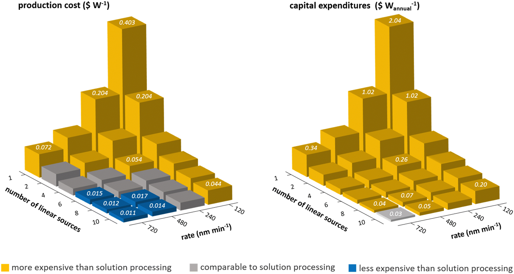 | ||
| Fig. 1 Basic techno-economic analysis for vapor processed perovskite absorbers. The number of linear sources as well as the deposition rates are found to be the most important parameters to achieve competitive production costs (left) and capital expenditures (right). Despite the often-claimed cost benefit of solution processing of perovskites, similar (gray) or better values (blue) are found for vapor processing if high enough rates can be accessed. Only the perovskite deposition step is considered here with the assumption that the other fabrication steps result in similar costs for solution and vapor processing. | ||
Status and outlook for vapor phase fabrication methods: how to become a game changer for the commercialization of perovskite photovoltaics?
Having discussed that from an economic point of view vapor-processed perovskite PV is generally able to compete with solution-based approaches, a comprehensive discussion covering key technological challenges of vapor-based techniques along with potential solutions are presented in the following. In agreement with the discussion before, it is highlighted that – to date – the slow throughput fabrication along with high CAPEX costs are the most critical aspects that hamper the implementation of vapor phase fabrication of perovskite PV on an industrial scale. Therefore, the first and foremost goal needs to be the development of competitive vapor deposition strategies capable of realizing (1) highly efficient absorber materials at (2) industrially viable throughput rates (dynamic deposition rates in industrial terminology) with (3) the lowest possible complexity of the deposition process, enabling a reliable process environment for a reproducible high-yield mass production with minimum demands on monitoring and process control. A major outcome of this discussion is the suggestion for more research and development on innovative deposition strategies besides the established co-evaporation approaches, such as sequential as well as closed-space or single-source deposition approaches.Performance
When it comes to the performance of vapor-processed perovskite absorbers, remarkable progress has been made recently by the extensive academic network (see Fig. S1 in the ESI†) – particularly for intensely investigated material compositions like single-cation materials (e.g., MAPbI3) and double-cation materials (e.g., CsFAPbI3). Not only are wide ranges of vapor-processed perovskite compositions steadily approaching thin-film qualities of their solution-based counterparts, but in some cases such as methylammonium-free compositions they outperform already today solution-processed absorbers (see Fig. 2).46,47 For this reason, it must be highlighted that the often-claimed preeminence in thin-film quality of solution-based approaches is most likely not founded on fundamental scientific limitations of vapor-based approaches, but rather just a result of the personnel and monetary disparity in research and development in the field, which resulted in a significant backlog for vapor processing over the years. In fact, one could likewise expect equal or even better thin-film qualities for vapor-processed perovskite materials given their simpler nucleation and thin-film formation processes as well as the absence of residual solvents and pinholes in the final thin film. It should be noted here that the vapor-processed CsFAPbI3 absorber employs PbCl2 as a crystallization agent while the solution-based reference does not. As PbCl2 in vapor processing acts similarly on the crystallization dynamics as the for example the exact choice of solvent systems or anti-solvent treatments in solution processing, the comparison chosen here is believed to be still reasonable.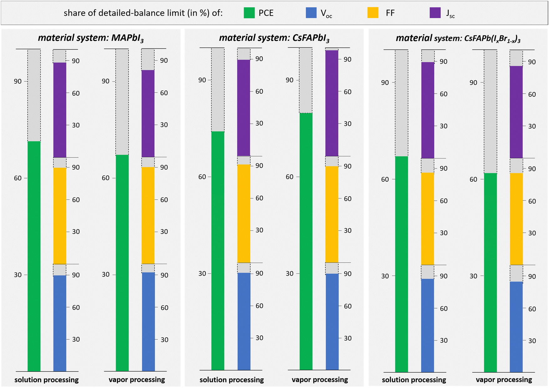 | ||
| Fig. 2 State-of-the-art achievements for vapor processed perovskite-based solar cells. Exemplary comparison of champion solar cells employing single- and double-cation hybrid perovskite absorbers prepared by either solution- (left) or vapor-based (right) approaches with respect to the theoretical detailed balance of the individual solar cell parameters. It is noted here that the figure does not provide a benchmark, but only revisits the state-of-the-art metrics of three prominent examples. MAPbI3 is highlighted here as it is still the most studied vapor processed perovskite material. CsFAPbI3 and CsFAPb(IxBr1−x)3 are examples for highly efficient vapor processed standard- and wide-bandgap materials. | ||
When comparing champion solar cells prepared with solution- or vapor-based perovskite absorbers (see Fig. 2 and Fig. S2 as well as Table S2 in the ESI†), the latter in many cases outperform their solution-based counterparts in terms of fill factor, given the improved uniformity and conformality of vapor-based deposition – characteristics that are of particular importance for the prevention of losses via shunt and series resistances at larger scales. However, lower open-circuit voltages and lower short-circuit current densities is often observed for vapor-based absorbers devices (see Tables S3 and S4 in the ESI†). Deficits in open-circuit voltage in vapor-processed perovskite solar cells are attributed to a generally lower opto-electronic absorber quality accompanied by the presence of non-passivated defect states inside the absorber as well as at its interfaces with adjacent charge transport layers, resulting in non-radiative recombination and in turn a limited maximum extractable open-circuit voltage of the solar cell.48–50 In fact, both photoluminescence quantum yield (PLQY) and charge carrier lifetimes of vapor-processed perovskite absorbers – especially for co-evaporated hybrid perovskite materials – have been shown to be up to one order of magnitude lower compared to their solution-processed counterparts,51 indicating a particular need for improvements of the bulk (and interface) quality of vapor-processed absorbers. In that regard, small grain sizes that are likely to come along with a significant number of detrimental grain boundary defects have been reported as an ongoing issue for the dominating co-evaporation processes. While methods to manipulate the vertical grain structure via adjustments of the employed substrate material have been reported,52 efforts to enlarge the lateral grain structure (e.g., via a fine-tuning of the substrate temperature) typically do not result in a similar improvement of the opto-electronic quality of the absorber.53,54 Therefore, a deeper understanding of how process parameters influence the morphological properties of vapor-processed perovskite absorbers and what currently limits the formation of higher quality absorbers is key for the further advancement of vapor-processed perovskite materials – also evident from existing learnings of already commercialized vapor-processed thin-film technologies like organic PV and organic LEDs.55 In that regard, deepening the understanding of crystallization kinetics for vapor-processed perovskite films in general is pivotal and needs to be further advanced by the research community – similarly to the progress that has been made for solution-processed films. Generally, it is believed that the complex evaporation characteristics in these co-evaporation approaches accompanied by a complex set of chemical interactions between the inorganic and organic compounds as well as potential decomposition products of the chemically fragile organic halides (see Discussion below),52,56–60 strain related effects,61,62 and the limited thermal stability of perovskite materials that restricts the use of high-temperature, diffusion-assisted deposition processes are the main reasons for the non-ideal crystallization dynamics and in turn small grain sizes.63–65 Furthermore, considering that significant morphological improvements in solution-processed approaches have been achieved by adding additives that slow down reaction rates (e.g., DMSO) or control crystal growth (e.g., alkylammonium chloride), it can be inferred that the lack of similar studies on these approaches for vapor-based processes is another reason for smaller grain sizes compared to the solution-based counterparts.66,67 Recently, alternative deposition strategies, particularly sequential deposition methods, have been shown to result in improved absorber morphologies with notable improvements in open-circuit voltages as a result of the changing film formation mechanism.46,47,68 Dynamic co-evaporation approaches including seed layer depositions have also shown promising improvements in film morphology and device performance.69,70 In addition, the formation and incorporation of decomposition products into the absorber can be circumvented by employing less harsh deposition procedures for the organic compound like hybrid methods (i.e., the vapor processing of the inorganic compounds and solution processing of the organic compounds).27–29 Nevertheless, the suitability of these two-step processes for the fabrication of high-quality perovskite absorbers particularly in an industrial setting still requires further confirmation and investigation.
While the concept of defect passivation of the perovskite absorber and its interfaces has been proven to be crucial for the realization of high-efficiency perovskite solar cells and is now a well-established strategy in solution-based approaches,71–73 the adoption of similar passivation approaches has been woefully neglected for vapor-based perovskite solar cells. Only a handful of studies investigated the influence of interface passivation for vapor-processed perovskite solar cells so far, however, always with a beneficial effect on the open-circuit voltage when integrated into the layer stack sequence.46,74,75 Most importantly, recent vapor-processed champion solar cells achieving power conversion efficiencies >24% employed a highly specialized passivation approach at the backside interface of the vapor-processed absorber, enabling an open-circuit voltage deficit of only 10%abs compared to its detailed balance limit, being on par with the solution-based counterparts with similar absorber composition.46,47 A stronger focus on the development and implementation of advanced passivation strategies is therefore a logical next step toward more competitive vapor processing of perovskite solar cells. Not only is the development of multi-interface passivation approaches that vastly reduces recombination at the interfaces between the absorber and charge transport layers crucial, but also considerations about how these approaches can be reasonably implemented in an industrial setting. The development of vapor-based passivation strategies that can be integrated directly into the absorber fabrication process are considered exceptionally suitable in that regard and should be particularly targeted by research and development.74 For the selection of potential passivation strategies, the extensive research that has already been performed on passivation strategies in solution-based approaches should be considered a helpful resource.
While losses in open-circuit voltage are mostly related to electrical losses in the device that affect vapor and solution-based absorbers alike, the typical reduction in short-circuit current density appears to be a particular issue for the vapor phase deposition of perovskite thin films. When comparing both fabrication approaches (see Fig. 2 and Fig. S2 in the ESI†), short-circuit current density deficits of solar cells employing vapor-processed perovskite absorbers are often up to 10%abs larger than those of their solution-based counterparts (see Tables S3 and S4 in the ESI†). First and foremost, the lack of suitable passivation strategies for vapor-processed perovskite absorbers does not only limit the open-circuit voltage but also indirectly influences the charge carrier extraction given the trade-off between increasing the absorber thickness to maximize current generation and decreasing thickness to keep recombination at an acceptable level. As a consequence, most vapor-processed perovskite solar cells still employ absorber thicknesses not exceeding 500 nm while high-efficient solution-based approaches with optimized passivation utilize absorbers as thick as 900 nm, enabling a close to perfect absorption of the incident sunlight. This emphasizes one more time the preeminent role the development of passivation strategies should play in the development of highly efficient vapor-processed perovskite solar cells. Moreover, lower short-circuit current densities can also be attributed to very planar vapor-processed perovskite thin films that provide neither light scattering nor a texture-induced facilitated light incoupling.
Throughput
When developing highly efficient vapor processing approaches, deposition rates need to be considered as the most important side constraint. Industrially viable deposition rates for the perovskite absorber should ideally be in the range of 1000 nm min−1 and above (synonymous with deposition times in the range of just one minute) to be able to compete with solution processing approaches as well as other thin-film PV technologies. Such high deposition rates in vapor processes have been demonstrated for other thin-film materials to be achievable in an industrial setting. For example, First Solar, Inc. successfully deposits its cadmium telluride absorbers at rates of 10![[thin space (1/6-em)]](https://www.rsc.org/images/entities/char_2009.gif) 000 nm min−1 and above using a technique called vapor transport deposition.76,77 Despite these encouraging achievements, vapor-based approaches for perovskite materials reported so far are rather slow-throughput approaches whose deposition rates typically do not exceed values of 10 nm min−1 – particularly for approaches that result in the highest performance (see Fig. 3). The overall deposition rate of a vapor process is affected by two parameters: (1) geometrical considerations of the deposition system and its evaporation sources and (2) fundamental temperature limitations of the employed precursor materials. Deposition rates can be significantly enhanced by increasing the number of consecutive deposition sources, increasing the evaporation area of the source, or by lowering the throw distance between sources and substrate. Up to date, academic research on vapor processing is focused on systems employing point-like evaporation sources, whose application in an industrial setting is considered to be of less relevance. For the further advancement of the throughput in vapor-processed perovskite absorbers, the development of alternative (e.g., linear or arial) source geometries and investigation of their suitability for the fabrication of uniform and reproducible perovskite thin films is considered crucial. In that regard, also the continuous operation of these sources (e.g., by adding appropriate powder feeding systems) needs to be investigated, as downtime for material replacement is considered a major bottleneck on the way toward high-throughput vapor processing of perovskite materials – particularly compared to fast solution-based printing techniques.
000 nm min−1 and above using a technique called vapor transport deposition.76,77 Despite these encouraging achievements, vapor-based approaches for perovskite materials reported so far are rather slow-throughput approaches whose deposition rates typically do not exceed values of 10 nm min−1 – particularly for approaches that result in the highest performance (see Fig. 3). The overall deposition rate of a vapor process is affected by two parameters: (1) geometrical considerations of the deposition system and its evaporation sources and (2) fundamental temperature limitations of the employed precursor materials. Deposition rates can be significantly enhanced by increasing the number of consecutive deposition sources, increasing the evaporation area of the source, or by lowering the throw distance between sources and substrate. Up to date, academic research on vapor processing is focused on systems employing point-like evaporation sources, whose application in an industrial setting is considered to be of less relevance. For the further advancement of the throughput in vapor-processed perovskite absorbers, the development of alternative (e.g., linear or arial) source geometries and investigation of their suitability for the fabrication of uniform and reproducible perovskite thin films is considered crucial. In that regard, also the continuous operation of these sources (e.g., by adding appropriate powder feeding systems) needs to be investigated, as downtime for material replacement is considered a major bottleneck on the way toward high-throughput vapor processing of perovskite materials – particularly compared to fast solution-based printing techniques.
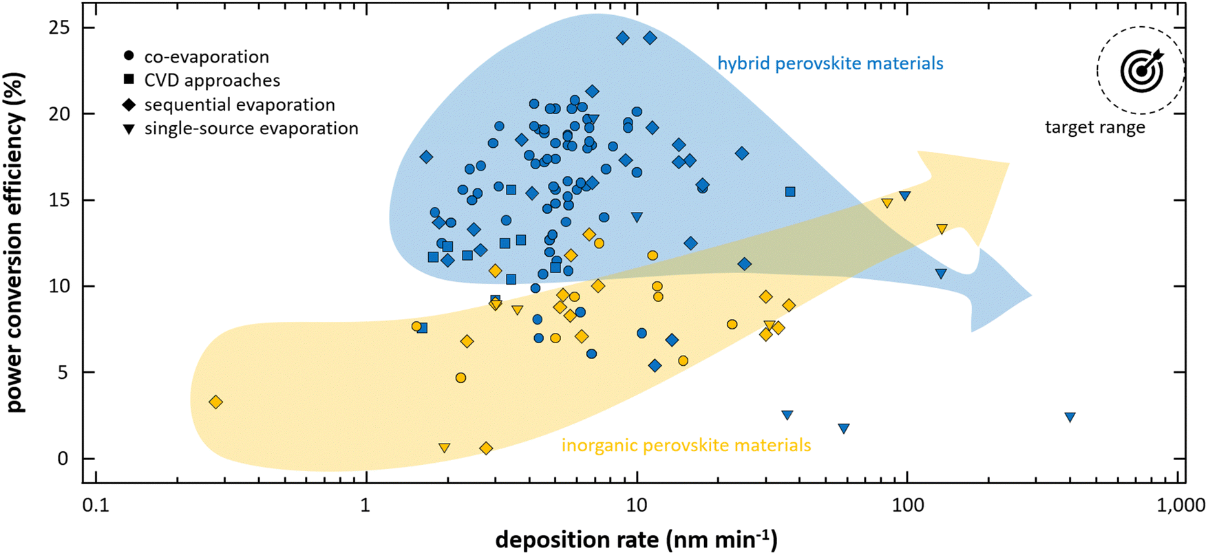 | ||
| Fig. 3 Deposition rates of vapor-processed perovskite absorbers. Summary of achieved power conversion efficiencies of perovskite solar cells based on vapor processed inorganic (yellow) and hybrid organic–inorganic (blue) perovskite absorbers as a function of deposition rates. Only the duration of the actual absorber deposition process without potential posttreatments is considered. Deposition processes that employ critical solution-based steps are not considered here. | ||
While for the development of industrially capable evaporation equipment major learnings can be directly translated from existing thin-film technologies, input from academia is vital for the development of intrinsically faster deposition processes. Most importantly, a thorough understanding of the limitations of established vapor processes and how they can be overcome is required. In that regard, a better understanding of the challenging evaporation characteristics of the organic halides is of particular importance. To date, high performance perovskite solar cells prepared by vapor-based approaches rely on the use of organic halides (i.e., methylammonium and formamidinium halides), which have been reported to show at least partial decomposition at elevated temperatures and in turn are limited to lower evaporation source temperatures (typically <200 °C), thus, slow deposition rates.59,60,78,79 The extent and impact of this decomposition are complex and hardly understood but experience in the field shows that the exact evaporation characteristics and interaction with the inorganic compounds deviate significantly between different organic halides (i.e., methylammonium vs. formamidinium halides) and may even be affected by other parameters like the purity level of the materials,80,81 the exact deposition process (i.e., co-evaporation vs. sequential methods), and the base pressure achievable inside the deposition chamber. Generally, the decomposition of methylammonium halides seems to be less detrimental as the reported main decomposition path (into highly volatile methylamine and hydrogen halides) is reversible, while for formamidinium halides stabile decomposition products (e.g., sym-triazine) can form whose effect on film formation and device performance is unknown yet.59,60,78,79 Overall, absorbers employing organic halides show a significant decline in performance when deposition rates (in point-source tools) are increased above a certain “comfort zone” (see Fig. 3). This might also limit the chance of success for single-source approaches in which organic and inorganic compounds are deposited from just one source, given the inevitable decomposition of the organic halides at the elevated temperatures required to simultaneously deposit the inorganic compounds. While alternative single-source techniques such as laser deposition or sputtering were proposed,44,82,83 they were not able to fully leave the “comfort zone” either because of lower performance or only limited improvements in deposition speed and proof of their suitability in an industrial setting is yet to be demonstrated. Classical multi-source co-evaporation approaches, which are the most successful approaches when it comes to versatility and performance on a laboratory scale, do not offer much room for improvements either (other than geometrical source considerations discussed before), as they are similarly limited by the maximum accessible deposition rate of the organic compounds. It is therefore not surprising that evaporation rates are stagnating when comparing the first reports on vapor-processed perovskite absorbers and recent champion solar cells (see Figure Tables S3 and S4 in the ESI†). Inorganic metal halides, on the other hand, are capable of withstanding significantly higher temperatures and better performances have been demonstrated for fully inorganic perovskite absorbers (e.g., CsPb(IxBr1−x)3) that are prepared at higher deposition rates (see Fig. 3). Moreover, recent work on continuous flash sublimation of inorganic perovskite solar cells was able to boost the deposition rates to values above 100 nm min−1 while at the same time exceeding the power conversion efficiency of significantly slower approaches.45 Even though these inorganic materials systems are capable of faster deposition rates, their application in a potential photovoltaic mass market is doubtful in the current stage of research given their challenging phase properties that negatively impact the stability of these materials.84 While a stronger focus on inorganic perovskite materials might not be the uppermost priority for the field, the high-quality, high-throughput deposition approaches developed for these inorganic halide materials can open promising routes for the high-throughput deposition in sequential deposition approaches.
In sequential deposition approaches (e.g., two-step approaches), the deposition of the organic and inorganic compounds is decoupled, facilitating in principle high-throughput deposition of the inorganic compound for example via a flash-sublimation approaches that is expected to achieve deposition times below one minute. In a second step, the organic compounds are then deposited on top of the inorganic layer and diffused into the inorganic framework in a subsequent annealing step. Similar approaches, still based on slow-paced depositions of the individual layers though, have recently demonstrated exciting performance of vapor-processed perovskite solar cells close to those of their solution-based counterparts, however, have not been independently reproduced in the community yet.46,47,68 While methods exist for the industrially compatible deposition of the inorganic compounds, processes for the fast incorporation of the organic compounds will require distinct efforts in research and development. Following industrially established methods in the optoelectronic mass market like vapor phase transport approaches, closed space sublimation, and other more chemically driven vapor deposition approaches might be promising routes for speeding up the deposition of the organic compounds, however, are currently less researched.43,85 Obviously, alternative methods for the deposition of the organic compounds will also benefit classical co-evaporation approaches and can boost their potential deposition rates. Alternatively, for most applications, the deposition of the organic compounds does not even have to be vapor based. Given the fact that both uniformity (e.g., for larger-area applications) and conformity (e.g., for tandem applications on top of textured surfaces) are primarily defined by the first deposition step, hybrid methods consisting of a vapor processing of the inorganic compounds followed by a fast solution deposition of the organic compound are considered equally suitable. Similar approaches have been successfully employed recently for the fabrication of some efficient tandem solar cells including fully textured monolithic tandem solar cells that exceed PCEs of 31%.27–29,86,87 Most importantly, these hybrid methods can introduce additional levers to control thin-film properties (e.g., for the development of absorber bulk passivation strategies) that are less accessible in the parameter-limited vapor-based approaches, however, at the same time they also add additional process complexity in an industrial setting given the complex interaction between the solid and liquid phases as well as the required handling of solvents. Most importantly, an interruption in the vacuum sequence when going from the vapor-based deposition of the inorganic layer to the solution-based deposition of the organic precursor and back to a vapor-based deposition of the charge extraction layer is required that is less favorable from an engineering and operational standpoint as it is believed to limit production throughput significantly.
Monitoring and process complexity
The success of the commercialization of a certain deposition approach not only depends on its performance and throughout but also greatly on the maturity of its complete industrial chain, which does not only include the deposition approach itself but also the availability and reliability of deposition and process monitoring equipment. The latter is a benefit of vapor-based approaches that have been employed for the fabrication of high-quality opto-electronic devices in an industrial mass market setting for decades. First Solar, Inc., the industry leader in both cumulative deployed thin-film photovoltaics and thin-film photovoltaics manufacturing capacity is a noteworthy example in that regard.88–90 For this reason, equipment manufacturers like the VON ARDENNE GmbH in Germany or Evolar AB in Sweden, the latter was recently acquired by First Solar Inc.,91 already preparing themselves for a future vapor processing of perovskite PV.92,93 Developing adapted processes that circumvent well-known challenges of state-of-the-art approaches (e.g., co-evaporation) is crucial. Research on co-evaporation approaches has revealed challenges for the process control and monitoring that are linked to the unique evaporation characteristics of the organic compounds. While the inorganic compounds evaporate rather directly, the organic compounds do not travel straight to the substrate and the formation of a high process pressure is typically observed, which adds additional complexity to the process. In turn, monitoring is aggravated by the comparably low sticking coefficients and/or surface dependent adsorption characteristics of the organic molecules on conventional quartz crystal monitors (QCMs), the additional reaction paths between organic and inorganic compounds (e.g., delayed conversion processes on the substrate that are not easily reflected in the detected rates by QCMs), or cross-reading effects if the organic compounds interact with QCMs positioned to primarily sample the inorganic deposition.52,56–58 Furthermore, impurities in the organic compound have been shown to also affect the rate detection.80,81 This can not only result in a lack of possibilities for a fine-tuning of material compositions but also limits reproducibility of co-evaporation approaches significantly when not taken into account. Kim et al. and Zanoni et al. have shown for the case of methylammonium iodide that the complex evaporation characteristic of the organic compound can be monitored more reliably if the combined rate of the organic and inorganic compound close to the substrate is monitored.81,94 Nevertheless, it needs to be evaluated whether the use of QCMs are suitable in an industrial setting and whether monitoring only the composition is a sufficient measure to evaluate the quality of the resulting thin films. In contrast to the OLED industry, where QCMs are commonly employed, the materials used for the fabrication of a perovskite absorber are of much higher density and processed thin films much thicker, reducing the available lifetimes of the QCMs significantly – particularity for high-throughput processes. Lifetime extending features including shutters and revolver-based multi-QCM systems will be required. Nevertheless, QCMs still might not be the first choice for continuous process monitoring. In general, research has shown that the quality of a perovskite absorber does not depend solely on the composition but its complete thin-film formation – both in solution- and vapor-based deposition approaches alike.95 For example, the complex interactions between the polar organic compounds (and their decomposition products) and the substrate material as well as process pressure, substrate temperature, and other process parameters have been shown to highly influence thin film formation and in turn device performance.52,96–98 It seems therefore necessary for a high-quality vapor process to expand the monitoring also to properties of the actual film formation (e.g., via electro-optical characterization methods), which is often employed in an industrial setting. For example, in situ reflectometry or photoluminescence spectroscopy are common low-cost techniques for in-line metrology and have recently been studied for vapor-processed perovskite materials as well.99 Furthermore, optical emission spectroscopy might be a way to continuously monitor the evaporation rates if the material fluxes are high enough. A stronger focus on the development and investigation of these alternative monitoring approaches for perovskite-based materials together with a general screening of more relevant process and thin-film characteristics is considered crucial for the advancement of vapor processing and its transfer to an industrial setting. Process control and monitoring as well as the overall process complexity will further benefit from a reduction of the number of individual evaporation sources in a system that have to be monitored. However, thin film quality and throughput cannot be compromised ultimately. In that regard, the authors highlight again the utmost urgency for the development for higher-rate deposition processes and equipment. Recent investigations on single source, laser, or sputtering approaches for the deposition of perovskites might be of particular interest.44,45,83,100,101 Sequential deposition strategies that decouple the deposition of inorganic and organic compounds might also be of interest as they circumvent some issues of the complex thin-film formation in co-evaporation by decoupling the monitoring of the composition and the film formation. For a practical application, further progress is also required in the development of deposition strategies that can be operated continuously. So far, most vapor-based deposition approaches reported in literature, particularly simultaneous deposition approaches, must be considered as batch approaches given the requirement for a regular replacement of the raw materials because of a loss in their quality when kept in a preheated evaporation boat for a prolonged time. While strategies for the continuous supply of the inorganic compounds have been reported,45 similar approaches do not exist for organic halide salts, highlighting again how crucial investigations about alternative incorporation methods of the organic compounds are not only for increasing deposition rates, as discussed above, but also for the general suitability of vapor-based approaches in an industrial setting.From laboratory to production – industry perspective for perovskite-based photovoltaics
Given the enormous potential, perovskite-based photovoltaics raises strong interest in industry. Not only has the outstanding progress in research led to the formation of several start-up companies around the globe, but also major established PV companies have announced to expand their research and development activities into the field. According to the 14th edition of the International Technology Roadmap for Photovoltaic,40 stakeholders from industry predict a market entry of some first between 2025 and 2027 (see also discussion below and Fig. S3 in the ESI†). In the following, a brief overview about current industrial activities in the field of perovskite-based PV is presented that will reveal unique insights into preferred deposition strategies. Global industrial activities in the field have been examined based on publicly accessible information (e.g., company homepages, press releases, social media posts, and job advertisements) between the end of 2021 and mid of 2023. In addition, the identified companies were directly approached to gain further insights into strategic company decisions – particularly about preferred deposition methods as well as expected commercialization dates. To the authors’ best knowledge, this collection of data represents a fair and comprehensive industry overview of perovskite-based PV industries. In total, 89 companies have identified to actively working in the field of perovskite-based PV in one of the three following business sectors: materials supply, deposition equipment manufacturing, and solar module manufacturing. A list of these companies together with basic publicly available information about them can be found in the ESI† (see Table S5 in the ESI†).The global distribution of perovskite industry clusters and their size is directly related to two distinct criteria: (1) the historic experience of certain regions in established PV technologies and (2) the research strength in the field of perovskite-based PV as well as ties between research and industry. East Asia, Europe, and North America are identified to have developed the most extensive industry clusters by size today (see Fig. 4). In accordance with their historic industrial strength, a strong interest in the perovskite PV technology from solar module manufacturers is present in China. In contrast to other world regions, this interest not only resulted in the formation of a number of early-stage companies (e.g., Microquanta Semiconductor Co. Ltd or Wuxi Utmolight Technology Co. Ltd),102,103 but is backed by a number of established major players in the silicon market. This includes JinkSolar or the LONGi Green Energy Technology Co. Ltd. that announced a fast growth and upscaling of perovskite-based tandem technologies.104,105 Similarly, also Japan shows a considerable interest where a number of well-known technology companies like the Panasonic Corporation, the Toshiba Corporation, or the Kaneka Corporation have announced the expansion of their research and development toward perovskites.106–108 However, the motivation for these companies seems to be different and the focus is more on the development of low-cost single junction perovskite solar cells as an alternative to silicon-based solar cells. Notably, the perovskite technology also stimulates interest in regions whose total solar module industry has not expanded vastly in the last decade. In that regard, lively activities with the formation of new solar module research and fabrication sites are observed for example in Europe and the United States. Both regions benefit from several early-stage companies (e.g., Saule Technologies, Oxford PV, or Swift Solar Inc.) as well as established companies such as the Meyer Burger Technology AG (Switzerland, Germany) or First Solar Inc. (United States) that have announced plans to integrate perovskites into their research and development focus.91,109–112 Noteworthy is also the extensive start-up environment with companies like CubicPV Technologies Inc., the Energy Materials Corporation, Swift Solar Inc., or TandemPV Inc. in the United States, which ranks highest worldwide by bare number.111,113–115 A major reason for this extensive network is the agile investment and funding environment in the United States but is further promoted by recent incentives of the U.S. administration including the Investing in America Agenda and the Inflation Reduction Act.116,117 Finally, also other business sectors next to solar module manufacturers prepare themselves for the commercialization of the perovskite technology. In that regard, both equipment manufacturers and materials suppliers are concentrated in regions that have a strong historic background in the production of process equipment or materials supply. A particularly strong industry cluster for process equipment is observed in Germany where companies like APEVA SE, the SINGULUS TECHNOLOGIES AG, or the VON ARDENNE GmbH commercialize large-area and high throughput process equipment for perovskite deposition.93,118,119 Moreover, other European companies like FOM Technologies (Denmark) as well as EVOLAR AB (Sweden), the latter of which was recently acquired by First Solar Inc. (United States), have positioned themselves in the field.92,120 With respect to materials suppliers – particularly for raw materials – successful companies are established worldwide ranging from East Asia (e.g., Tokyo Chemical Industry Co. Ltd. (Japan) or the Luminescence Technology Corporation (Taiwan)) to Europe and Australia (e.g., Greatcell Energy Pty. Ltd (Australia) or Dyenamo AB (Sweden)).121–124 For an extended list of companies that were identified to working in the field, the reader is referred to Table S5 in the ESI.†
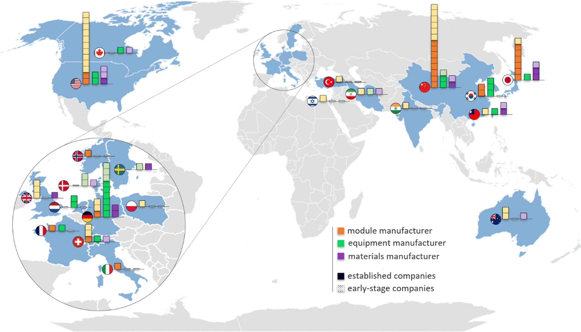 | ||
| Fig. 4 Global distribution of industrial activities in the field of perovskite-based photovoltaics. Distribution of the 89 companies identified in this work working in the field of perovskite-based photovoltaics separated into the three business sectors materials supply, deposition equipment manufacturers, and solar module manufacturers. Individual companies have been counted several times in case their business model expands over different business sectors. Early-stage companies are marked in light colors. | ||
When it comes to the deposition techniques that companies target to employ for the industrial scale deposition of perovskite materials, this industry outlook reveals a strong interest in vapor phase deposition processes worldwide (see Fig. 5a). In stark contrast to the previously discussed heavy focus of scientific publications on solution processing, around 40% of all identified module manufacturers and 70% of all equipment manufacturers stated activities in vapor phase deposition or combinations of vapor phase deposition and solution processing for the scalable processing of perovskite thin films. The interest in vapor phase deposition processes is manifested in all large industry clusters worldwide (East Asia, Europe, and North America). Furthermore, among the established solar module manufacturers, i.e., those solar module manufacturers that already have a significant production capacity in place, the importance of vapor phase deposition processes is even stronger. Out of the 15 world-largest solar module manufacturers by annual production capacity (i.e., in the silicon and CdTe business), seven companies have been identified to actively work on perovskite PV, with six companies evaluating either vapor phase processing or a combination of vapor phase and solution processing. The motivation of these major players to rely nearly exclusively on (partial) vapor phase processing is attributed to their interest in combining perovskite materials with established PV technologies in monolithic multi-junction solar cells. Despite the outstanding progress of tandem solar cells employing solution-based deposited perovskite absorbers in research, the high-quality deposition on textured surfaces, the high production yield and reproducibility, as well as the simple integration into existing production lines are key decision criteria that warrant the use of vapor phase deposition in this potentially most important application of perovskite materials. While also attracting significant interest from established companies, solution processing of perovskite PV appears to be dominated by early-stage companies for both solar module and equipment manufacturing (see Fig. 5b). In contrast to manufacturers that target the production of multi-junction solar modules, the focus of these companies in many cases is on the development of high-throughput single-junction solar modules making use of a direct transfer of the extensive process know-how for solution processing from research to industrial fabrication. Activities on vapor processing of perovskite materials are backed up by a significant number of tool manufacturers (as well as materials suppliers that are, however, less specific to a certain deposition method) that commercialize processing tools for vapor phase processes – i.e., several tool manufacturers stated market entry of production line ready tools starting from 2024 onwards. This is just in time, considering that most solar module manufacturers state commercialization dates of first products starting from 2025 onwards (see Fig. S3 in the ESI†). First movers like Oxford PV have even released commercialization dates as early as 2023/2024 which seems ambitious given several bottlenecks (e.g., operational durability) of the technology are still not completely solved yet. In summary, despite the fact that the vast majority of research studies makes use of solution-processed perovskite thin films, vapor phase deposition processes have already found their way to an industrial setting and gain more and more momentum. As research and development of vapor-processed perovskite thin films is still heavily underrepresented in literature, their full industrial potential is yet to be identified.
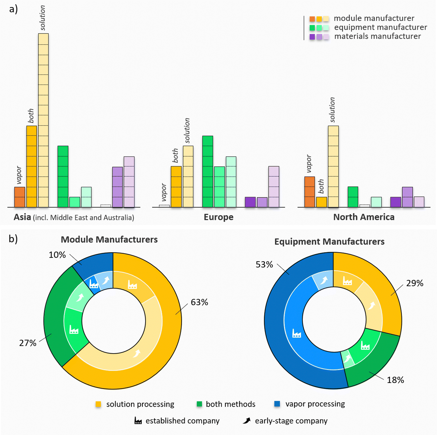 | ||
| Fig. 5 Deposition focuses of industrial manufacturing of perovskite PV and related business sectors. (a) Number of companies employing certain deposition techniques by business sector and region. (b) Worldwide share of different deposition techniques for module and equipment manufacturing for established and early-stage companies. This information has been collected by an industry survey or via publicly available information as outlined in the ESI.† | ||
Outlook
Can vapor phase deposition of perovskite thin films be a short track to a successful commercialization of perovskite PV? Here, we highlight the conceptional advantages of vapor phase processing and rationalize why we believe a stronger focus on these methods is pivotal for of the commercialization of perovskite PV. Worldwide, perovskite PV is progressing rapidly toward commercialization, with the first solar module manufacturers expected to enter the market by 2024/2025. Despite this rapid progress, it is yet unknown which fabrication technology – solution-based, vapor-based, or combinations – will eventually pave the way toward the economic breakthrough at the terawatts scale. Today, all major global technology clusters, i.e., North America, Europe, and East Asia, encompass stakeholders with a focus on solution-based as well as vapor-based processing of perovskite thin films.This perspective highlights the tremendous technological and economical potential of vapor phase deposition of perovskite thin films for PV manufacturing at industrial scale. The prime archetype for scalable, high-yield, and high-throughput perovskite PV manufacturing is the established thin-film PV industry (e.g., CdTe, CIGS, as well as organic PV and OLED industry), which is widely based on vapor phase processing. It is therefore not surprising, that also for perovskite-based PV a notable interest from industry on vapor-based deposition is again observed. The interest is particularly driven by recent advances in performance of vapor-based perovskite solar cells with certified PCEs up to 24.1%, which continue to close the gap to their solution-processed counterparts. A large variety of different vapor phase processes have been explored in research, including co-evaporation, sequential evaporation, and hybrid processing methods. Compared to their solution-based counterparts, vapor phase processes stand out due to their solvent-free, homogeneous, and pinhole-free deposition on planar and textured substrates. The latter is particularly critical for the manufacturing of monolithic tandem solar cells in combination with textured silicon, which are expected to become the first commercial perovskite product with major market share. While it is often claimed that solution-based processing promises lower production and lower capital expenditure costs, our basic techno-economic analysis reveals that for high deposition rates and large-scale manufacturing tools, vapor phase processing can compete with solution processing in both categories, provided that key challenges of vapor processing are solved: first, state-of-the-art performance with respect to efficiency and durability needs to be achieved, motivating further research efforts with respect to perovskite compositions, charge transport layers, passivation strategies, and device architectures. Second, high-rate vapor phase processes (particularly for the organic halides) need to be developed that speed up the deposition by at least one to two orders of magnitude. To date, sequential vapor-phase processes may offer the highest, however, still too slow dynamic deposition rates. Research on new high-rate deposition concepts like closed-space sublimation, flash sublimation, or sputtering approaches as well as the exploration of industrial designs for evaporation sources has just started and needs to be emphasized. Finally, in order to enable high-yield and large-scale production, efficient and robust process regimes need to be identified and methods for reliable monitoring developed. In this regard, a better understanding of the evaporation characteristics of the precursor materials and the thin-film formation processes during vapor phase deposition along with the development of in situ and in-line monitoring techniques for efficient process control are crucial.
Next to addressing the aforementioned key challenges of vapor phase deposition processes, future materials research targeting higher performance, durability, and manufacturability needs to place a much stronger emphasis on vapor-processed perovskite PV. According to our industry surveys, close to half of the companies in the field state activities on vapor phase deposition processes, while the vast majority of scientific studies focus on solution processing (i.e., more than 99% of all studies published in 2021). Considering this stark contrast and the pressing timeline for commercialization, there is an urge for global research and development activities to support the industrial developments by investing much more effort and shifting resources toward the advancement of vapor phase processing of perovskite thin films.
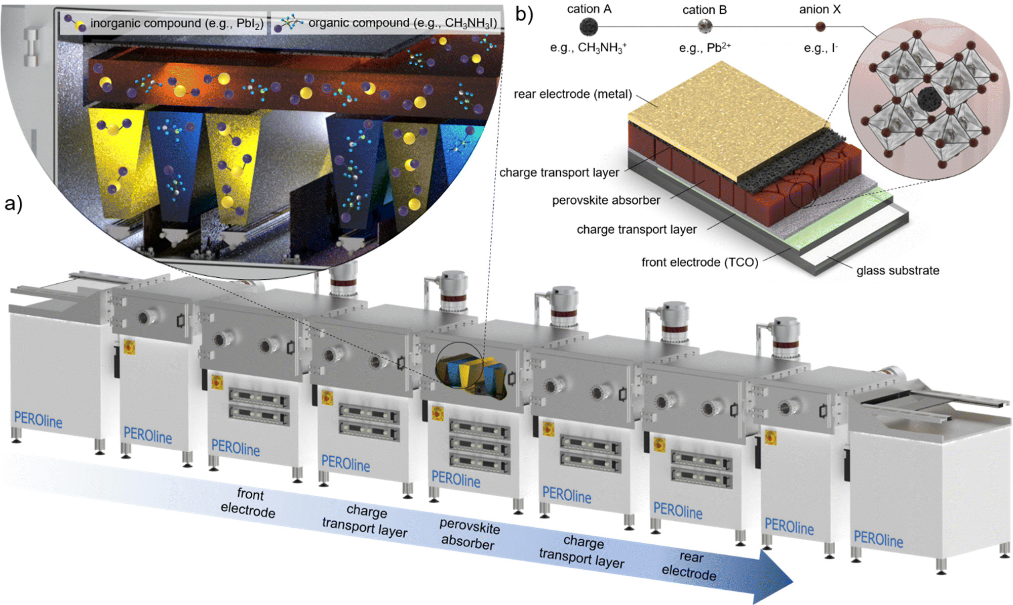
Box 1: Vapor phase deposition of halide perovskite semiconductors in a nutshellVapor phase deposition belongs to the most advanced and successful industrial fabrication techniques for opto-electronic thin films. It is not surprising that these techniques also play a crucial role for the development of halide perovskite semiconductors and their application particularly in solar cells.125–127 In fact, vapor phase deposition of halide perovskite thin films by multi- and single-source approaches were already employed by Era et al. and Mitzi et al., respectively, in the late 1990s.128,129 Even though these studies did not identify the semiconducting characteristic of halide perovskite materials, they evaporated these layers a decade before the demonstration of the first solar cell employing a halide perovskite material by Kojima et al. in 2006.130 Since these early attempts, the concept of vapor phase deposition has not changed significantly and can be categorized into three approaches: (1) the deposition of pre-prepared powder or films from a single source (single-source approach), (2) the simultaneous deposition of several individual precursor materials (co-deposition approach), and (3) the sequential deposition of individual precursor materials (layer-by-layer approach). To date, co-deposition is by far the most researched approach as it enables simple tuning of the thin-film composition with evaporation equipment commonly employed in research.In vapor-based approaches, one or more precursor materials (e.g., one organic and one inorganic halide salt) are vaporized simultaneously or sequentially by increasing their vapor pressure above the surrounding pressure inside a vacuum chamber kept under high-vacuum conditions (∼10−5 mbar range). While the energy for transferring the precursor materials into their vapor state is in most cases supplied by radiation energy from electrically powered heating wires wrapped around an IR-transparent crucible or by direct contact of the precursor materials with a high-temperature surface in special evaporation boats, other energy sources including high-energy electron beams, laser radiation, or electric arcs are similarly suitable. Following the transfer of the vaporized molecules through the vacuum chamber, condensation of the molecules on a cold (compared to the thermal energy of the molecules) substrate surface takes place that is accompanied by the nucleation and crystallization of a high-purity thin film. The composition of the resulting thin film, which is tuned by the ratio of organic and inorganic salts reaching the substrate, can be readily monitored by quartz crystal monitors (QCMs) in real time.81,131 The crystallization kinetics of vapor-processed perovskite films differs fundamentally from solution-processed films and is subject to ongoing research and development. Liu et al. demonstrated for the first time the suitability of the co-evaporation approach for the fabrication of perovskite solar cell absorbers in 2013 by simultaneously depositing lead chloride (PbCl2) and methylammonium iodide (CH3NH3I) resulting in a first solar cell with a power conversion efficiency (PCE) of 15.4%.132 In addition, it was shown that next to complex mesoporous device architectures mostly employed in solution-processed solar cells, planar layer stack sequences are similarly suitable for the fabrication of efficient perovskite-based solar cells, simplifying the fabrication process significantly. Having paved the way for the general applicability of vapor-based deposition techniques, a fast rise in research activity on vapor-processed perovskite absorbers was observed that ultimately resulted in the demonstration of solar cells with PCEs >24%,46,47 only slightly lower than for their solution-based counterparts with record PCEs of 26%.1 In addition, good long-term stability for up to 3,600 h at 85 °C has been proven for unencapsulated perovskite solar cells employing co-deposited absorbers, which might be even higher than for comparable solution-processed devices.133 This progress is particularly remarkable considering the overall rather small community (with a share of perovskite related publications of less than 1%) researching that field compared to the broad community investigating solution-based approaches.31 Reasons for the fast improvement in performance are related to (1) a better understanding of the chemical processes taking place during co-deposition of organic and inorganic salts,59,60,65,81,94,97 (2) a better understanding of the growth mechanism during the co-deposition and the influence of substrate surface properties on it,52,54,97,98 (3) as well as the use of alternative absorber composition next to methylammonium lead iodide (CH3NH3PbI3).68,75,134–136 A particularity of the simultaneous co-deposition approaches, already observed in early studies,56–58 is the omnidirectional sublimation characteristic of the organic halide salts given their low enthalpy of evaporation and vulnerability to decomposition.59,60,137 Depending on the design of the vacuum chamber, this particularity can complicate the monitoring of the individual deposition rates and influences the composition of the deposited thin films. In response, some research groups employed cold surfaces inside the vacuum chamber to adsorb the omnidirectional evaporation component39,54,134 as well as monitoring approaches via multiple QCMs.81,94 In addition, alternative deposition approaches are researched.43,44,138,139 Important progress was made by gaining insights into the film formation mechanisms during co-deposition. For example, a strong influence of the substrate material's surface properties on the crystallographic and morphological properties of the resulting thin film was found,96–98 insights that enabled a better screening of suitable materials the absorber is deposited onto.52 Of particular interest for an industrial application of vapor-processed perovskite solar cells are fully evaporated layer stack sequences, in which all functional layers of the solar cell are prepared by vapor-based approaches. The concept was pioneered by Polander et al. in 2014, who achieved fully evaporated perovskite solar cells with PCEs as high as 10.9%,140 and applied and refined in the meantime by others.52,141–145 Particularly, these concepts lower the complexity of the fabrication process compared to mixed approaches also employing solution-based approaches and most importantly enable a simple upscaling of the deposition process toward industrially relevant device areas. First promising prototype solar modules have been demonstrated,37,38,143,146 exhibiting low upscaling losses comparable to other much longer researched thin-film technologies.39 Finally, applying vapor-processed perovskite solar cells in tandem applications – for example in combination with textured silicon bottom solar cells – open promising applications that can significantly enhance the performance of established PV technologies.147 As a result of the high conformity of vapor-deposited layers, high-quality film formation can be achieved even on highly textured silicon bottom solar cells,85,148–150 which is usually tricky to access by solution-based approaches.151 First fully textured perovskite-silicon tandem solar cells employing vapor-processed deposition techniques for the deposition of the top perovskite solar cell have been demonstrated recently achieving PCEs exceeding 30%.28,86,135,152 Furthermore, solvent incompatibilities make vapor processing also a highly relevant deposition technique for monolithic all-perovskite tandem solar cells.75,137 Given the outstanding scientific progress achieved in shortest time as well as their beneficial properties, vapor-processed perovskite solar cells are indeed considered to play an important role in the industrialization of the perovskite PV technology. Fig. B1 General concept of vapor processing of perovskite solar cells. (a) Concept for the in-line fabrication of fully vapor-processed perovskite solar cells together with the general processes taking place during the co-evaporation of organic and inorganic compounds (see enlarged detail). (b) Sample layer stack sequence for opaque perovskite solar cells. |
Conflicts of interest
There are no conflicts to declare.Acknowledgements
The work performed at the National Renewable Energy Laboratory (NREL) was supported by the U.S. Department of Energy's Office of Energy Efficiency and Renewable Energy (EERE) under Solar Energy Technologies Office (SETO) Agreement Number DE-EE0009017 and NREL, operated by the Alliance for Sustainable Energy, LLC, for the U.S. Department of Energy (DOE) under contract number DE-AC36-08GO28308. The views expressed in the article do not necessarily represent the views of the DOE or the U.S. Government. The U.S. Government retains and the publisher, by accepting the article for publication, acknowledges that the U.S. Government retains a nonexclusive, paid-up, irrevocable, worldwide license to publish or reproduce the published form of this work, or allow others to do so, for U.S. Government purposes.The authors furthermore acknowledge the support by the Federal Ministry for Economic Affairs and Climate Action of Germany under grant agreement 03EE1123A (project SHAPE) as well as the European Union through HORIZON EUROPE Research and Innovation Actions under grant agreement number 101075330 (project NEXUS). Views and opinions expressed are those of the authors only and do not necessarily reflect those of the European Union or the European Climate, Infrastructure and Environment Executive Agency (CINEA). Neither the European Union nor the granting authority can be held responsible.
Financial support for the creation of the cover artwork by the Ministry of Trade, Industry, and Energy of the Republic of Korea under the grant agreement 202300302107 was highly appreciated.
The authors further recognize the kind worldwide support by the many companies in the field of perovskite-based photovoltaics that contributed to the industry survey and gave us first-hand insights into the commercialization of this technology.
References
- National Renewable Energy Laboratory (NREL). Best Research-Cell Efficiency Chart. (2023). Available at: https://www.nrel.gov/pv/cell-efficiency.html.
- S. De Wolf,
et al., Organometallic halide perovskites: sharp optical absorption edge and its relation to photovoltaic performance, J. Phys. Chem. Lett., 2014, 5, 1035–1039 CrossRef CAS PubMed
.
- G. W. Kim and A. Petrozza, Defect Tolerance and Intolerance in Metal-Halide Perovskites, Adv. Energy Mater., 2020, 10, 1–6 Search PubMed
- D. W. Dequilettes,
et al., Photoluminescence Lifetimes Exceeding 8 μs and Quantum Yields Exceeding 30% in Hybrid Perovskite Thin Films by Ligand Passivation, ACS Energy Lett., 2016, 1, 438–444 CrossRef CAS
- X. Yang,
et al., Superior Carrier Lifetimes Exceeding 6 μs in Polycrystalline Halide Perovskites, Adv. Mater., 2020, 32, 6–13 Search PubMed
- L. M. Herz, Charge-Carrier Mobilities in Metal Halide Perovskites: Fundamental Mechanisms and Limits, ACS Energy Lett., 2017, 2, 1539–1548 CrossRef CAS
- M. R. Filip, G. E. Eperon, H. J. Snaith and F. Giustino, Steric engineering of metal-halide perovskites with tunable optical band gaps, Nat. Commun., 2014, 5, 1–9 Search PubMed
- H. J. Snaith, Present Status and Future Prospects of Perovskite Photovoltaics, Nat. Mater., 2018, 17, 372–376 CrossRef CAS PubMed
- Y. Rong,
et al., Challenges for commercializing perovskite solar cells, Science, 2018, 361, eaat8235 CrossRef PubMed
- Y. Cheng and L. Ding, Pushing commercialization of perovskite solar cells by improving their intrinsic stability, Energy Environ. Sci., 2021, 14, 3233–3255 RSC
- N. Moody,
et al., Assessing the Regulatory Requirements of Lead-Based Perovskite Photovoltaics, Joule, 2020, 4, 970–974 CrossRef
- A. Kojima, K. Teshima, Y. Shirai and T. Miyasaka, Organometal halide perovskites as visible-light sensitizers for photovoltaic cells, J. Am. Chem. Soc., 2009, 131, 6050–6051 CrossRef CAS PubMed
- Q. Jiang,
et al., Surface reaction for efficient and stable inverted perovskite solar cells, Nature, 2022, 611, 278–283 CrossRef CAS PubMed
- D. K. Lee and N. G. Park, Materials and Methods for High-Efficiency Perovskite Solar Modules, Sol. RRL, 2022, 6, 1–25 Search PubMed
- Y. Deng,
et al., Scalable fabrication of efficient organolead trihalide perovskite solar cells with doctor-bladed active layers, Energy Environ. Sci., 2015, 8, 1544–1550 RSC
- H. Hu,
et al., Room-Temperature Meniscus Coating of >20% Perovskite Solar Cells: A Film Formation Mechanism Investigation, Adv. Funct. Mater., 2019, 29, 1–12 Search PubMed
- J. Yang, E. L. Lim, L. Tan and Z. Wei, Ink Engineering in Blade-Coating Large-Area Perovskite Solar Cells, Adv. Energy Mater., 2022, 12, 2200975 CrossRef CAS
- R. Patidar, D. Burkitt, K. Hooper, D. Richards and T. Watson, Slot-die coating of perovskite solar cells: an overview, Mater. Today Commun., 2020, 22, 100808 CrossRef CAS
- K. Xu,
et al., Slot-Die Coated Triple-Halide Perovskites for Efficient and Scalable Perovskite/Silicon Tandem Solar Cells, ACS Energy Lett., 2022, 7, 3600–3611 CrossRef CAS PubMed
- J. Li,
et al., Ink Design Enabling Slot-Die Coated Perovskite Solar Cells with >22% Power Conversion Efficiency, Micro-Modules, and 1 Year of Outdoor Performance Evaluation, Adv. Energy Mater., 2023, 2203898 CrossRef CAS
- J. E. Bishop, C. D. Read, J. A. Smith, T. J. Routledge and D. G. Lidzey, Fully Spray-Coated Triple-Cation Perovskite Solar Cells, Sci. Rep., 2020, 10, 1–8 CrossRef PubMed
- H. Cai, X. Liang, J. Su and J. Guan, High Efficiency Over 20% of Perovskite Solar Cells by Spray-Coating via a Simple Process High Efficiency Over 20% of Perovskite Solar Cells by Spray-Coating via a Simple Process, ACS Appl. Energy Mater., 2020, 3, 9696–9702 CrossRef CAS
- L.-H. Chou, J. M. W. Chan and C.-L. Liu, Progress in Spray Coated Perovskite Films for Solar Cell Applications, Sol. RRL, 2022, 6, 2101035 CrossRef CAS
- F. Mathies,
et al., Multipass Inkjet Printed Planar Methylammonium Lead Iodide Perovskite Solar Cells, J. Mater. Chem. A, 2016, 4, 19207 RSC
- F. Mathies, E. J. W. List-Kratochvil and E. L. Unger, Advances in Inkjet-Printed Metal Halide Perovskite Photovoltaic and Optoelectronic Devices, Energy Technol., 2020, 8, 1900991 CrossRef CAS
- H. Eggers,
et al., Inkjet-Printed Micrometer-Thick Perovskite Solar Cells with Large Columnar Grains, Adv. Energy Mater., 2020, 10, 1–12 Search PubMed
- F. Fu,
et al., Low-temperature-processed efficient semi-transparent planar perovskite solar cells for bifacial and tandem applications, Nat. Commun., 2015, 6, 1–9 Search PubMed
- F. Sahli,
et al., Fully Textured Monolithic Perovskite/Silicon Tandem Solar Cells with 25.2% Power Conversion Efficiency, Nat. Mater., 2018, 17, 820–826 CrossRef CAS PubMed
- W. Soltanpoor,
et al., Hybrid Vapor-Solution Sequentially Deposited Mixed-Halide Perovskite Solar Cells, ACS Appl. Energy Mater., 2020, 3, 8257–8265 CrossRef CAS
- L. Tan,
et al., Combined Vacuum Evaporation and Solution Process for High-Efficiency Large-Area Perovskite Solar Cells with Exceptional Reproducibility, Adv. Mater., 2023, 35, 2205027 CrossRef CAS PubMed
- T. J. Jacobsson,
et al., An open-access database and analysis tool for perovskite solar cells based on the FAIR data principles, Nat. Energy, 2022, 7, 107–115 CrossRef CAS
- I. A. Howard,
et al., Coated and Printed Perovskites for Photovoltaic Applications, Adv. Mater., 2019, 31, 1806702 CrossRef PubMed
- F. Yang,
et al., Upscaling Solution-Processed Perovskite Photovoltaics, Adv. Energy Mater., 2021, 11, 2101973 CrossRef CAS
- B. Geffroy, P. le Roy and C. Prat, Organic light-emitting diode (OLED) technology: materials, devices and display technologies, Polym. Int., 2006, 55, 572–582 CrossRef CAS
- G. Hong,
et al., A Brief History of OLEDs—Emitter Development and Industry Milestones, Adv. Mater., 2021, 33, 2005630 CrossRef CAS PubMed
- J. Y. Woo,
et al., Advances in Solution-Processed OLEDs and their Prospects for Use in Displays, Adv. Mater., 2022, 2207454 Search PubMed
- J. Li,
et al., Highly Efficient Thermally Co-evaporated Perovskite Solar Cells and Mini-modules, Joule, 2020, 4, 1035–1053 CrossRef CAS
- J. Li,
et al., Design of Perovskite Thermally Co-Evaporated Highly Efficient Mini-Modules with High Geometrical Fill Factors, Sol. RRL, 2020, 4, 2000473 CrossRef CAS
- D. B. Ritzer,
et al., Upscaling of perovskite solar modules: the synergy of fully evaporated layer fabrication and all-laser-scribed interconnections, Prog. Photovoltaics Res. Appl., 2022, 30, 360–373 CrossRef CAS
-
Verband Deutscher Maschinen- und Anlagenbau e.V. (VDMA). International Technology Roadmap for Photovoltaic (ITRPV), 14th edn, 2023 Search PubMed
- U.S. Department of Energy. The SunShot Initiative. (2011). Available at: https://www.energy.gov/eere/solar/sunshot-initiative.
-
B. L. Smith, et al., Photovoltaic Module Technologies: 2020 Benchmark Costs and Technology Evolution Framework Results, 2021 Search PubMed
- M. T. Hoerantner,
et al., High-Speed Vapor Transport Deposition of Perovskite Thin Films, ACS Appl. Mater. Interfaces, 2019, 11, 32928–32936 CrossRef CAS PubMed
- B. Gao,
et al., Organic–Inorganic Perovskite Films and Efficient Planar Heterojunction Solar Cells by Magnetron Sputtering, Adv. Sci., 2021, 8, 1–10 Search PubMed
- T. Abzieher, et al., Continuous Flash Sublimation of Inorganic Halide Perovskites: Overcoming Rate and Continuity Limitations of Vapor Deposition, 2024, submitted.
- H. Li,
et al., Sequential vacuum-evaporated perovskite solar cells with more than 24% efficiency, Sci. Adv., 2022, 8, 1–9 Search PubMed
- H. Li,
et al., Molten Salt Strategy for Reproducible Evaporation of Efficient Perovskite Solar Cells, Adv. Funct. Mater., 2022, 33, 2211232 CrossRef
- P. Caprioglio,
et al., On the Relation between the Open-Circuit Voltage and Quasi-Fermi Level Splitting in Efficient Perovskite Solar Cells, Adv. Energy Mater., 2019, 9, 1901631 CrossRef
- P. Caprioglio,
et al., Open-circuit and short-circuit loss management in wide-gap perovskite p–i–n solar cells, Nat. Commun., 2023, 14, 1–13 Search PubMed
- L. Krückemeier, B. Krogmeier, Z. Liu, U. Rau and T. Kirchartz, Understanding Transient Photoluminescence in Halide Perovskite Layer Stacks and Solar Cells, Adv. Energy Mater., 2021, 11, 2003489 CrossRef
- I. Susic,
et al., Combinatorial Vacuum-Deposition of Wide Bandgap Perovskite Films and Solar Cells, Adv. Mater. Interfaces, 2023, 10, 2202271 CrossRef CAS
- T. Abzieher,
et al., From Groundwork to Efficient Solar Cells: On the Importance of the Substrate Material in Co-Evaporated
Perovskite Solar Cells, Adv. Funct. Mater., 2021, 31, 2104482 CrossRef CAS
- K. B. Lohmann,
et al., Control over Crystal Size in Vapor Deposited Metal-Halide Perovskite Films, ACS Energy Lett., 2020, 5, 710–717 CrossRef CAS PubMed
- M. Roß,
et al., Co-Evaporated p–i–n Perovskite Solar Cells beyond 20% Efficiency: Impact of Substrate Temperature and Hole-Transport Layer, ACS Appl. Mater. Interfaces, 2020, 12, 39261–39272 CrossRef PubMed
- F. Yang, M. Shtein and S. R. Forrest, Morphology control and material mixing by high-temperature organic vapor-phase deposition and its application to thin-film solar cells, J. Appl. Phys., 2005, 98, 014906 CrossRef
- J. Teuscher, A. Ulianov, O. Müntener, M. Grätzel and N. Tétreault, Control and Study of the Stoichiometry in Evaporated Perovskite Solar Cells, ChemSusChem, 2015, 8, 3847–3852 CrossRef CAS PubMed
- B. S. Kim, M. H. Choi, M. S. Choi and J. J. Kim, Composition-controlled organometal halide perovskite Via CH3NH3I pressure in a vacuum co-deposition process, J. Mater. Chem. A, 2016, 4, 5663–5668 RSC
- S. Y. Hsiao,
et al., Efficient All-Vacuum Deposited Perovskite Solar Cells by Controlling Reagent Partial Pressure in High Vacuum, Adv. Mater., 2016, 28, 7013–7019 CrossRef CAS PubMed
- M. J. Bækbo, O. Hansen, I. Chorkendorff and P. C. K. Vesborg, Deposition of methylammonium iodide: via evaporation-combined kinetic and mass spectrometric study, RSC Adv., 2018, 8, 29899–29908 RSC
- M. Kroll,
et al., Insights into the evaporation behaviour of FAI: material degradation and consequences for perovskite solar cells, Sustainable Energy Fuels, 2022, 6, 3230–3239 RSC
- H. S. Kim and N. G. Park, Importance of tailoring lattice strain in halide perovskite crystals, NPG Asia Mater., 2020, 12, 78 CrossRef CAS
- D. Liu,
et al., Strain analysis and engineering in halide perovskite photovoltaics, Nat. Mater., 2021, 20, 1337–1346 CrossRef CAS PubMed
- T. Burwig and P. Pistor, Reaction kinetics of the thermal decomposition of MAPbI3 thin films, Phys. Rev. Mater., 2021, 5, 1–13 Search PubMed
- T. Burwig, K. Heinze and P. Pistor, Thermal decomposition kinetics of FAPbI3 thin films, Phys. Rev. Mater., 2022, 6, 065404 CrossRef CAS
- P. Pistor, T. Burwig, C. Brzuska, B. Weber and W. Fränzel, Thermal stability and miscibility of co-evaporated methyl ammonium lead halide (MAPbX3, X = I, Br, Cl) thin films analysed by: in situ X-ray diffraction, J. Mater. Chem. A, 2018, 6, 11496–11506 RSC
- N. J. Jeon,
et al., Solvent engineering for high-performance inorganic–organic hybrid perovskite solar cells, Nat. Mater., 2014, 13, 897–903 CrossRef CAS PubMed
- J. Park,
et al., Controlled growth of perovskite layers with volatile alkylammonium chlorides, Nature, 2023, 616, 724–730 CrossRef CAS PubMed
- J. Feng,
et al., High-throughput large-area vacuum deposition for high-performance formamidine-based perovskite solar cells, Energy Environ. Sci., 2021, 14, 3035–3043 RSC
- K. L. Heinze,
et al., Importance of methylammonium iodide partial pressure and evaporation onset for the growth of co-evaporated methylammonium lead iodide absorbers, Sci. Rep., 2021, 11, 1–12 CrossRef PubMed
- R. Heidrich,
et al., Impact of dynamic co-evaporation schemes on the growth of methylammonium lead iodide absorbers for inverted solar cells, Sci. Rep., 2022, 12, 1–11 CrossRef PubMed
- B. Chen, P. N. Rudd, S. Yang, Y. Yuan and J. Huang, Imperfections and their passivation in halide perovskite solar cells, Chem. Soc. Rev., 2019, 48, 3842–3867 RSC
- F. Gao, Y. Zhao, X. Zhang and J. You, Recent Progresses on Defect Passivation toward Efficient Perovskite Solar Cells, Adv. Energy Mater., 2020, 10, 1902650 CrossRef CAS
- Y. Cao,
et al., Defects Passivation Strategy for Efficient and Stable Perovskite Solar Cells, Adv. Mater. Interfaces, 2022, 9, 2200179 CrossRef CAS
- M. G. La-Placa,
et al., Vacuum-Deposited 2D/3D Perovskite Heterojunctions, ACS Energy Lett., 2019, 4, 2893–2901 CrossRef CAS
- Y. Chiang,
et al., Vacuum-Deposited Wide-Bandgap
Perovskite for All-Perovskite Tandem Solar Cells, ACS Energy Lett., 2023, 8, 2728–2737 CrossRef CAS PubMed
- J. M. Kestner,
et al., An experimental and modeling analysis of vapor transport deposition of cadmium telluride, Sol. Energy Mater. Sol. Cells, 2004, 83, 55–65 CrossRef CAS
-
R. C. Powell, Research Leading to High Throughput Manufacturing of Thin-Film CdTe PV Modules: Annual Technical Report, 2004 Search PubMed
- E. J. Juarez-Perez, L. K. Ono and Y. Qi, Thermal degradation of formamidinium based lead halide perovskites into sym-triazine and hydrogen cyanide observed by coupled thermogravimetry-mass spectrometry analysis, J. Mater. Chem. A, 2019, 7, 16912–16919 RSC
- A. Luongo, B. Brunetti, S. Vecchio Ciprioti, A. Ciccioli and A. Latini, Thermodynamic and Kinetic Aspects of Formamidinium Lead Iodide Thermal Decomposition, J. Phys. Chem. C, 2021, 125, 21851–21861 CrossRef CAS PubMed
- J. Borchert,
et al., Impurity Tracking Enables Enhanced Control and Reproducibility of Hybrid Perovskite Vapor Deposition, ACS Appl. Mater. Interfaces, 2019, 11, 28851–28857 CrossRef CAS PubMed
- K. P. S. Zanoni, L. Martínez-Goyeneche, C. Dreessen, M. Sessolo and H. J. Bolink, Photovoltaic Devices Using Sublimed Methylammonium Lead Iodide Perovskites: Long-Term Reproducible Processing, Sol. RRL, 2023, 2201073, 1–9 Search PubMed
- T. Soto-Montero,
et al., Single-Source Vapor-Deposition of MA1−xFAxPbI3 Perovskite Absorbers for Solar Cells, Adv. Funct. Mater., 2023, 2300588 CrossRef
- T. Soto-Montero, et al., Single-Source Pulsed Laser Deposited Perovskite Solar Cells with >19% Efficiency, Preprin, 2023.
- W. Xiang, S. Liu and W. Tress, A review on the stability of inorganic metal halide perovskites: Challenges and opportunities for stable solar cells, Energy Environ. Sci., 2021, 14, 2090–2113 RSC
- F. Sahli,
et al., Vapor Transport Deposition of Methylammonium Iodide for Perovskite Solar Cells, ACS Appl. Energy Mater., 2021, 4, 4333–4343 CrossRef CAS
- L. Mao,
et al., Fully Textured, Production-Line Compatible Monolithic Perovskite/Silicon Tandem Solar Cells Approaching 29% Efficiency, Adv. Mater., 2022, 34, 2206193 CrossRef CAS PubMed
- X. Y. Chin,
et al., Interface passivation for 31.25%-efficient perovskite/silicon tandem solar cells, Science, 2023, 381, 59 CrossRef CAS PubMed
-
R. C. Powell, Research Leading to High-Throughput Manufacturing of Thin-Film CdTe PV Modules, 2006 Search PubMed
- S. Kurtz,
et al., Historical Analysis of Champion Photovoltaic Module Efficiencies, IEEE J. Photovoltaics, 2018, 8, 363–372 Search PubMed
- D. Feldman, et al., Spring 2022 Solar Industry Update, 2022.
- First Solar Inc. First Solar Strengthens Global Technology Position in PV with Acquisition of Evolar, a Leading European Thin Film Company. (2023). Available at: https://investor.firstsolar.com/news/press-release-details/2023/First-Solar-Strengthens-Global-Technology-Position-in-PV-with-Acquisition-of-Evolar-a-Leading-European-Thin-Film-Company/default.aspx.
- EVOLAR AB. Company Homepage. (2023). Available at: https://www.evolarab.se/.
- VON ARDENNE GmbH. Company Homepage. (2023). Available at: https://vonardenne.com/.
- B. S. Kim, L. Gil-Escrig, M. Sessolo and H. J. Bolink, Deposition Kinetics and Compositional Control of Vacuum-Processed CH3NH3PbI3 Perovskite, J. Phys. Chem. Lett., 2020, 11, 6852–6859 CrossRef CAS PubMed
- J. Bing, S. Huang and A. W. Y. Ho-Baillie, A Review on Halide Perovskite Film Formation by Sequential Solution Processing for Solar Cell Applications, Energy Technol., 2020, 8, 1–22 Search PubMed
- H. Xu,
et al., Formation and Evolution of the Unexpected PbI2 Phase at the Interface during the Growth of Evaporated Perovskite Films, Phys. Chem. Chem. Phys., 2016, 18, 18607 RSC
- S. Olthof and K. Meerholz, Substrate-Dependent Electronic Structure and Film Formation of MAPbI3 Perovskites, Sci. Rep., 2017, 7, 40267 CrossRef CAS PubMed
- J. B. Patel,
et al., Influence of Interface Morphology on Hysteresis in Vapor-Deposited Perovskite Solar Cells, Adv. Electron. Mater., 2017, 3, 1–6 Search PubMed
- V. Held,
et al., Evolution of Structure and Optoelectronic Properties During Halide Perovskite Vapor Deposition, J. Phys. Chem. Lett., 2022, 13, 11905–11912 CrossRef CAS PubMed
- T. Soto-Montero,
et al., Single-Source Vapor-Deposition of MA1−xFAxPbI3 Perovskite Absorbers for Solar Cells, Adv. Funct. Mater., 2023, 2300588 CrossRef
- M. Tai,
et al., Efficient Inorganic Cesium Lead Mixed-Halide Perovskite Solar Cells Prepared by Flash-Evaporation Printing, Energy Technol., 2019, 7, 1–6 CrossRef
- Microquanta Semiconductor Co. Ltd. Company Homepage. (2023). Available at: https://www.microquanta.com/en/.
- Wuxi Utmolight Technology Co. Ltd. Company Homepage. (2023). Available at: https://www.utmolight.com/en/.
- pv magazine. JinkoSolar announces perovskite cell technology platform promising efficiencies close to 30%. (2021). Available at: https://www.pv-magazine.com/2021/06/25/jinkosolar-announces-perovskite-cell-technology-platform-promising-efficiencies-close-to-30/.
- pv magazine. Longi claims 33.5% efficiency for perovskite/silicon tandem solar cell. (2023). Available at: https://www.pv-magazine.com/2023/06/15/longi-claims-33-5-efficiency-for-perovskite-silicon-tandem-solar-cell/.
- Panasonic Corporation. Japan's NEDO and Panasonic Achieve the World's Highest Conversion Efficiency of 16.09% for Largest-area Perovskite Solar Cell Module. (2020). Available at: https://news.panasonic.com/global/press/en200207-2.
- Toshiba Corporation. Toshiba's Polymer Film-Based Perovskite Large-Area Photovoltaic Module Reaches Record Power Conversion Efficiency of 15.1%. (2021). Available at: https://www.global.toshiba/ww/technology/corporate/rdc/rd/topics/21/2109-01.html.
- Kaneka Corporation. Kaneka to Accelerate Development to Social Implementation of High-Performance Perovskite Solar Cells via the NEDO Green Innovation Fund. (2022). Available at: https://www.kaneka.co.jp/en/topics/news/ 2022, https:///ennr2203162.html.
- Saule Technologies. Company Homepage. (2023). Available at: https://sauletech.com/.
- Oxford PV. Company Homepage. (2023). Available at: https://www.oxfordpv.com/.
- Swift Solar Inc. Company Homepage. (2023). Available at: https://www.swiftsolar.com/.
- Meyer Burger Technology AG. Meyer Burger establishes new partnerships for the development of high-performance solar modules with perovskite technology. Available at: https://www.meyerburger.com/pl/newsroom/artikel/meyer-burger-establishes-new-partnerships-for-the-development-of-high-performance-solar-modules-with-perovskite-technology.
- CubicPV Technologies Inc. Company Homepage. (2023). Available at: https://cubicpv.com/.
- Energy Materials Corp. Company Homepage. (2023). Available at: https://enmatcorp.com/advanced-photovoltaic-material-manufacturing/.
- TandemPV Inc. Company Homepage. (2023). Available at: https://www.tandempv.com/.
- The White House. President Joe Biden: Investing in America. (2023). Available at: https://www.whitehouse.gov/invest/.
- The White House. Inflation Reduction Act Guidebook. (2023). Available at: https://www.whitehouse.gov/cleanenergy/inflation-reduction-act-guidebook/.
- AIXTRON SE. Company Homepage. (2023). Available at: https://www.aixtron.com/en.
- SINGULUS TECHNOLOGIES AG. Company Homepage. (2023). Available at: https://www.singulus.com/.
- FOM Technologies. Company Homepage. (2023). Available at: https://www.fomtechnologies.com/.
- Tokyo Chemical Industry Co. Ltd. Company Homepage. (2023). Available at: https://www.tcichemicals.com/ID/en.
- Luminescence Technology Corporation. Company Homepage. (2023). Available at: https://lumtec.com.tw/.
- Greatcell Energy Pty. Ltd. Company Homepage. (2023). Available at: https://www.greatcellenergy.com/.
- Dyenamo AB. Company Homepage. (2023). Available at: https://dyenamo.se/.
- J. Ávila, C. Momblona, P. P. Boix, M. Sessolo and H. J. Bolink, Vapor-Deposited Perovskites: The Route to High-Performance Solar Cell Production?, Joule, 2017, 1, 431–442 CrossRef
- Y. Vaynzof, The Future of Perovskite Photovoltaics—Thermal Evaporation or Solution Processing?, Adv. Energy Mater., 2020, 10, 2003073 CrossRef CAS
- Q. Guesnay, F. Sahli, C. Ballif and Q. Jeangros, Vapor deposition of metal halide perovskite thin films: process control strategies to shape layer properties, APL Mater., 2021, 9, 1–21 Search PubMed
- M. Era, T. Hattori, T. Taira and T. Tsutsui, Self-organized growth of PbI-based layered perovskite quantum well by dual-source vapor deposition, Chem. Mater., 1997, 9, 8–10 CrossRef CAS
- D. B. Mitzi, M. T. Prikas and K. Chondroudis, Thin Film Deposition of Organic–Inorganic Hybrid Materials Using a Single Source Thermal Ablation Technique, Chem. Mater., 1999, 11, 542–544 CrossRef CAS
- A. Kojima, K. Teshima, T. Miyasaka and Y. Shirai, Novel Photoelectrochemical Cell with Mesoscopic Electrodes Sensitized by Lead-Halide Compounds (2). in Proceedings of the 210th ECS Meeting, Cancun, Mexico (2006).
- B. S. Kim, L. Gil-Escrig, M. Sessolo and H. J. Bolink, Deposition Kinetics and Compositional Control of Vacuum-Processed CH3NH3PbI3 Perovskite, J. Phys. Chem. Lett., 2020, 11, 6852–6859 CrossRef CAS PubMed
- M. Liu, M. B. Johnston and H. J. Snaith, Efficient Planar Heterojunction Perovskite Solar Cells by Vapour Deposition, Nature, 2013, 501, 395–398 CrossRef CAS PubMed
- H. A. Dewi,
et al., Excellent Intrinsic Long-Term Thermal Stability of Co-Evaporated MAPbI3 Solar Cells at 85 °C, Adv. Funct. Mater., 2021, 31, 2100557 CrossRef CAS
- Y. H. Chiang, M. Anaya and S. D. Stranks, Multisource Vacuum Deposition of Methylammonium-Free Perovskite Solar Cells, ACS Energy Lett., 2020, 5, 2498–2504 CrossRef CAS PubMed
- M. Roß,
et al., Co-Evaporated Formamidinium Lead Iodide Based Perovskites with 1000 h Constant Stability for Fully Textured Monolithic Perovskite/Silicon Tandem Solar Cells, Adv. Energy Mater., 2021, 11, 2104160 Search PubMed
- K. B. Lohmann,
et al., Solvent-Free Method for Defect Reduction and Improved Performance of p–i–n Vapor-Deposited Perovskite Solar Cells, ACS Energy Lett., 2022, 1903–1911 CrossRef CAS PubMed
- D. Forgács,
et al., Efficient Monolithic Perovskite/Perovskite Tandem Solar Cells, Adv. Energy Mater., 2017, 7, 1–6 Search PubMed
- Q. Guo,
et al., The growth of a CH3NH3PbI3 thin film using simplified close space sublimation for efficient and large dimensional perovskite solar cells, Energy Environ. Sci., 2016, 9, 1486–1494 RSC
- M. M. Tavakoli,
et al., Fabrication of efficient planar perovskite solar cells using a one-step chemical vapor deposition method, Sci. Rep., 2015, 5, 1–9 Search PubMed
- L. E. Polander,
et al., Hole-transport material variation in fully vacuum deposited perovskite solar cells, APL Mater., 2014, 2, 081503 CrossRef
- C. Momblona,
et al., Efficient vacuum deposited p-i-n and n-i-p perovskite solar cells employing doped charge transport layers, Energy Environ. Sci., 2016, 9, 3456–3463 RSC
- B.-S. Kim, T.-M. Kim, M.-S. Choi, H.-S. Shim and J.-J. Kim, Fully vacuum-processed perovskite solar cells with high open circuit voltage using MoO3/NPB as hole extraction layers, Org. Electron., 2015, 17, 102 CrossRef CAS
- T. Abzieher,
et al., Electron-Beam-Evaporated Nickel Oxide Hole Transport Layers for Perovskite-Based Photovoltaics, Adv. Energy Mater., 2019, 9, 1802995 CrossRef
- M. M. Tavakoli, P. Yaday, D. Prochowicz and R. Tavakoli, Efficient, Hysteresis-Free and Flexible Inverted Perovskite Solar Cells Using All-Vacuum Processing, Sol. RRL, 2020, 2000552 Search PubMed
- D. Pérez-del-Rey, P. P. Boix, M. Sessolo, A. Hadipour and H. J. Bolink, Interfacial Modification for High-Efficiency Vapor-Phase-Deposited Perovskite Solar Cells Based on a Metal Oxide Buffer Layer, J. Phys. Chem. Lett., 2018, 9, 1041 CrossRef PubMed
- H. Eggers,
et al., Perovskite Solar Cells with Vivid, Angle-Invariant, and Customizable Inkjet-Printed Colorization for Building-Integrated Photovoltaics, Sol. RRL, 2022, 6, 2100897 CrossRef CAS
- F. Fu,
et al., Monolithic Perovskite-Silicon Tandem Solar Cells: From the Lab to Fab?, Adv. Mater., 2022, 34, 2106540 CrossRef CAS PubMed
- L. Cojocaru,
et al., Detailed Investigation of Evaporated Perovskite Absorbers with High Crystal Quality on Different Substrates, ACS Appl. Mater. Interfaces, 2018, 10, 26293–26302 CrossRef CAS PubMed
- T. Abzieher,
et al., Efficient All-Evaporated pin-Perovskite Solar Cells: A Promising Approach Toward Industrial Large-Scale Fabrication, IEEE J. Photovoltaics, 2019, 9, 1249–1257 Search PubMed
- L. Gil-Escrig,
et al., Fully Vacuum-Processed Perovskite Solar Cells on Pyramidal Microtextures, Sol. RRL, 2021, 5, 1–9 Search PubMed
- M. Jošt, L. Kegelmann, L. Korte and S. Albrecht, Monolithic Perovskite Tandem Solar Cells: A Review of the Present Status and Advanced Characterization Methods Toward 30% Efficiency, Adv. Energy Mater., 2020, 10, 1904102 CrossRef
- pv magazine. CSEM, EPFL achieve 31.25% efficiency for tandem perovskite-silicon solar cell (2022). Available at: https://www.pv-magazine.com/2022/07/07/csem-epfl-achieve-31-25-efficiency-for-tandem-perovskite-silicon-solar-cell/.
Footnote |
| † Electronic supplementary information (ESI) available. See DOI: https://doi.org/10.1039/d3ee03273f |
| This journal is © The Royal Society of Chemistry 2024 |