Design and fabrication of a microfluidic SERS chip with integrated Ag film@nanoAu
Hua-Zhou Zhaoabc,
Yi Xu*abc,
Chun-Yan Wangbcd,
Rong Wangabc,
Song-Tao Xiangabc and
Li Chen*bcd
aSchool of Chemistry and Chemical Engineering, Chongqing University, Chongqing, 400030, China. E-mail: xuyibbd@sina.com
bDefense Key Disciplines Lab of Novel Micro-nano Devices and System Technology, Chongqing, 400030, China. E-mail: CL2009@cqu.edu.cn
cInternational R & D Center of Micro-nano Systems and New Materials Technology, Chongqing, 400030, China
dSchool of Optoelectronic Engineering, Chongqing University, Chongqing, 400030, China
First published on 22nd January 2016
Abstract
A “sandwich” microfluidic surface enhanced Raman scattering (SERS) chip with Ag film@nanoAu prepared in a microchannel was proposed and fabricated in situ. The integrated composite Ag film@nanoAu was prepared in situ by way of chemical plating and self-assembly. Firstly, the preparation conditions were optimized. On the basis of that, the influence of the laser focus position along the vertical direction and the materials of the cover plates on the SERS effect were investigated and optimized in detail. The optimized SERS effect was observed when the laser was focused on the interface of the sample and the SERS substrate. The SERS intensity of Rhodamine 6G (R6G) decreased 2.5 times and 2.1 times when PDMS or glass was used as the cover plate separately. Compared to single gold and silver SERS substrates, the composite of Ag film@nanoAu integrated in the microfluidic channel resulted in the peak intensity increasing 3–5 times during the SERS detection of R6G at 1507 cm−1. The enhancing effect could be attributed to the change in the local electromagnetic field which was caused by the synergistic sensitizing effect between the Au nanoparticles and the underlying silver mirror film. It was illustrated that the detection limit for R6G was 10−8 M and the enhancement factor (EF) was 3.8 × 10⁵ with a relative standard deviation (RSD) of approximately 10% in the as-prepared microfluidic SERS chip.
1. Introduction
Microfluidic technology has several advantages such as high efficiency of analysis, minimal sample requirement, short reaction time and less waste generation.1,2 However, the minimal sample requires a high-sensitivity detection method. Currently, various detection methods, for example, LIF, UV-visible absorption, chemiluminescence, and Raman spectroscopy have been applied for on-chip detection.2 Among the various optical detection methods, Raman spectroscopy has been proven to be highly compatible with microfluidics,3 because it can provide fingerprint information of species and needs a short detection time. But the scattering cross-sections of Raman scattering are very low, and the Raman signal is only about 10−10 times the intensity of the incident laser,4 which means that low concentrations of species can hardly be detected. SERS can extremely enhance the Raman intensity due to the interaction of molecules with a rough, nanostructured metallic surface, and the detection sensitivity is enhanced by up to 6–10 orders of magnitude over conventional Raman spectroscopy.5,6 Integrating a SERS substrate into a microfluidic channel not only provides an efficient detection platform for LoC systems but also improves the SERS signal reproducibility.7,8 Additionally, the analytes in the microfluidic chip are not easily contaminated, which to some extent, leads to a high signal-to-noise ratio (SNR).9When SERS was chosen as the detector for microfluidic chips, there were two common approaches, i.e. mixing the sample with a gold or silver colloid in the microfluidic channel or passing the sample through the microfluidic channels integrated with the SERS substrate.10 The former was restricted in its application due to the poor stability and reproducibility of colloidal nanoparticles.8,11 Meanwhile, the latter attracted wide attention because of its advantages of controllable preparation of SERS substrates and the superior stability and reproducibility of the SERS signals.12,13 At present, much more attention has been paid to the research of the latter one, especially to the integration of a SERS substrate which was of high intensity, good stability and reproducibility into the microfluidic channel and the construction of a kind of microfluidic SERS chip with excellent sensitivity and stability.
In recent years, micro electromechanical system (MEMS) processing technology has become the most common method for preparing SERS substrates in microfluidic chips, which includes soft lithography, nanosphere lithography, physical vapor deposition (PVD),14–16 and so on. The SERS substrates constructed in this way are of an orderly structure and uniform distribution of SERS “hot spots”.15,17–20 But, MEMS technology is limited due to its special requirement for processing equipment, complex process, high cost and because it is subjected to restrictions of materials. Physical/chemical methods, such as electrochemical deposition, chemical deposition, plasma and self-assembly methods,21–23 have attracted extensive attention in the fields of microfluidic SERS chips due to their advantages of flexible operation, inexpensive equipment and not being limited by the material. Electrodeposition and galvanic replacement reactions are usually used to fabricate silver nanoparticle-decorated nanowall structures in microfluidic channels.24 A polyol method was conducted to fabricate nanostructured Ag thin films in a microfluidic patterning system.25 However, the physical/chemical method is currently in its infancy, and there exist many problems, such as little research of SERS substrates integrated in microfluidic chips, poor sensitivity and reproducibility of the SERS signal and so on.
Generally, Ag and Au are regarded as the best candidates for SERS substrates.26–29 It is well known that silver nanoparticles exhibit strong SERS scattering properties.30 But, silver is relatively active and susceptible to surface oxidation, while gold is both biocompatible and highly resistant to oxidation.31 Silver film could be protected from oxidation by adsorbing gold nanoparticles onto its surface. Meanwhile, a synergistic effect would be observed when these two were combined together. Therefore, composite nano-structures have become a focal point for SERS research.
According to the excellent plasma characteristics and synergistic effect of silver and gold nanoparticles as SERS substrates, a composite structure of Ag film@nanoAu as a SERS substrate was designed and fabricated in situ in a self-designed PDMS–PDMS–glass “sandwich” microfluidic channel in this paper. At first, the silver film was derived through the silver mirror reaction, and then gold nanoparticles were deposited on it using a self-assembly-chemical plating process. In order to obtain better coordination of the SERS enhancing effect in the microfluidic channels, rhodamine 6G was chosen as the probe molecule and preparation conditions of the composite SERS substrate and the coordination enhancement effect between gold and silver were studied. Furthermore, the influence of the laser focus position along the vertical direction and the materials of the cover plates on the SERS signal were investigated in detail. Finally, a comprehensive evaluation of the derived microfluidic SERS chip could be conducted.
2. Experimental
2.1 Reagents and equipment
Deionized water was used for all aqueous solutions. Hydrogen tetrachloroauric acid (HAuCl4·4H2O, AR) was purchased from Sinopharm chemical reagent Co. Ltd, silver nitrate (AgNO3, AR) from Aladdin, hydroxylamine hydrochloride (NH2OH·HCl, AR) from Chengdu KeLong Chemical, poly dimethyl diallyl ammonium chloride (PDDA, 35 wt%, AR) from Heowns, Rhodamine 6G (R6G, AR) from Sigma, the SU-8 photoresist and developer from Microchem, and poly(dimethylsiloxane) from Dow Corning (Sylgard 184). And all the other reagents were of analytical reagent (AR) grade and purchased from Chongqing Chuandong chemical group.A gold colloid was prepared according to Frens.32 A 10 mg sample of HAuCl4·4H2O was dissolved in 100 mL of DI water. The solution was brought to boil while being stirred. Next, 8 mL of 1% sodium citrate was added rapidly, and the solution was boiled for another 20 min.
The preparation of fresh silver–ammonia solution was according to the method of Chen:33 2% ammonia solution was added dropwise to 2% AgNO3 solution until the precipitate just disappeared.
2.2 Equipment
Confocal microscopic Raman spectrometer (HORIBA LABRAM, France). Scanning electron microscope (SEM) (Hitachi 7800F system, Japan).2.3 Preparation of “sandwich” microfluidic chip
The “sandwich” microfluidic chip consisted of three layers, as shown in Fig. 1a. A normal glass substrate was used as the bottom layer, a PDMS layer with a microchannel in the middle and a PDMS or glass cover layer at the top. The glass substrate was cleaned ultrasonically with hot sodium hydroxide solution for ten minutes before use. Then it was soaked in fresh “piranha” solution for 30 min. After that, it was further rinsed using DI water and dried with nitrogen gas. The middle layer of the PDMS microchannel was fabricated using soft-lithography technology. Briefly, the SU-8 photoresist was spin-coated for 500 μm thickness and was prebaked for 30 min to evaporate the organic solvent. A 500 μm high, 500 μm wide and 3 cm long template was successfully prepared by UV-lithography. Then, the polydimethylsiloxane (PDMS) prepolymer and a curing agent were thoroughly mixed in a 10![[thin space (1/6-em)]](https://www.rsc.org/images/entities/char_2009.gif) :
:![[thin space (1/6-em)]](https://www.rsc.org/images/entities/char_2009.gif) 1 weight ratio. Subsequently, the mixture was poured onto the surface of the pre-prepared SU-8 template, and cured for 1 h at a temperature of 90 °C. When the PDMS was dried, it was peeled off from the template and the PDMS channel was derived. The PDMS cover plate with a thickness of 1 mm was fabricated in the same way. Holes were punched through the cover plate at both ends of the channel, and were utilized as inlet and outlet respectively. The normal glass substrate, PDMS middle layer and cover plate were rinsed with acetone, anhydrous ethanol and DI water in turn and were bonded together to form a “sandwich” microfluidic chip.
1 weight ratio. Subsequently, the mixture was poured onto the surface of the pre-prepared SU-8 template, and cured for 1 h at a temperature of 90 °C. When the PDMS was dried, it was peeled off from the template and the PDMS channel was derived. The PDMS cover plate with a thickness of 1 mm was fabricated in the same way. Holes were punched through the cover plate at both ends of the channel, and were utilized as inlet and outlet respectively. The normal glass substrate, PDMS middle layer and cover plate were rinsed with acetone, anhydrous ethanol and DI water in turn and were bonded together to form a “sandwich” microfluidic chip.
 | ||
| Fig. 1 (a) Components for the “sandwich” microfluidic chip; (b) cross section for the microfluidic channel with integrated SERS substrate. | ||
2.4 Fabrication of Ag film@nanoAu substrate in the microfluidic channel
For fabrication in situ of the highly active SERS substrate, the chip was firstly flushed with 0.02% SnCl2 solution to improve the adhesion of the Ag film onto the glass surface. Then, a mixture of newly prepared silver–ammonia solution and 5% glucose was filled into the channel for 10 minutes in a 60 °C water bath and the silver mirror film was derived. For self-assembled AuNPs on the Ag film, concentrations of 0.1%, 0.3%, 0.5%, and 1% (wt%) PDDA solution were injected into the chip before assembling. After standing for 30 min and thoroughly rinsing with DI water, the prepared gold colloid was injected into the channel and allowed to stand for 6 h. During the process, the gold colloid in the channel was replaced by fresh gold colloid every 30 min. After that, the chemical plating solution with a content of 0.2 mM of hydroxylammonium chloride and 0.1% hydrogen tetrachloroauric acid was passed through the channel at a speed of 20 μL min−1 and the reaction times were 0, 2, 4, 6, 8, and 10 min. Finally, the microfluidic SERS chip with Ag film@nanoAu was obtained (Fig. 2). It is important to mention that the cover plate should be cleaned before SERS detection.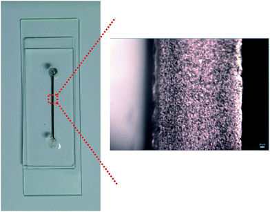 | ||
| Fig. 2 The image of the whole microfluidic chip and the optical image of the Ag@nanoAu embedded microfluidic channel. | ||
The structure and surface morphology of the Ag film@nanoAu were characterized using scanning electron microscopy (SEM) (Hitachi 7800F system).
2.5 Detection of R6G in the designed microfluidic SERS chip
In order to observe and evaluate the performance and effect of the prepared Ag film@nanoAu in the microfluidic chip, SERS spectra of series samples of R6G solution were measured on a confocal microscopic Raman spectrometer (HORIBA LABRAM) equipped with a He–Ne laser at 633 nm as an excitation source and the excitation power was about 17 mW. The spectral resolution of this instrument was 2 cm−1 and the spectrograph used 1800 g mm−1 gratings. R6G solutions with different concentrations of 10−8 M, 10−7 M, 10−6 M, 10−5 M, and 10−4 M were injected into the microchip and the Raman scattering spectra were collected through a 50 × microscope objective lens (NA 0.5) with a focal spot of about 1 μm in diameter and an acquisition time of 4 s. In addition, a neutral density filter of 10% was alternated for decreasing the laser power on the samples.3. Results and discussion
3.1 Design and fabrication of Ag film@nanoAu microstructure
The PDMS–PDMS–glass sandwich chip was designed as shown in Fig. 1a. By utilizing the excellent plasma characteristics of gold and silver, and the virtues of gold with good stability and biocompatibility, as well as being not easily oxidized, the novel complex SERS nanostructure of Ag film@nanoAu was designed and fabricated. The Ag thin film was deposited in the microfluidic chip firstly via the silver mirror reaction. Gold nanoparticles were immobilized on the silver mirror film by a self-assembly-chemical plating method. It has been demonstrated that possible SERS active sites were at their junctions, which induced the increasing of the “hot spot” density of the system.27,34 The Ag film@nanoAu presented here was expected to have high local electromagnetic (EM) field enhancement and could serve as a SERS substrate for molecular sensing. Additionally, considering the advantage of in situ preparation, the inner-wall of the microchannel was covered completely by Ag film@nanoAu (Fig. 1b), which might limit the incident laser within the tiny size of the microchannel, and reduce the spread of the incident laser. Thus, the maximum Raman scattering signals of the samples were collected. The density of gold nanoparticles distributed on the silver mirror film was controlled by altering the concentration of PDDA, the size and interparticle distance of the gold nanoparticles were adjusted by varying the chemical plating time.The density of Au nanoparticles adsorbed on the Ag film was an important factor for obtaining a highly active Ag film@nanoAu in the microfluidic chip.35 As shown in Fig. 3, with the increasing concentration of PDDA, the SERS intensity of R6G decreased gradually when the chemical plating time was 4 min. This could be explained as follows: with the increasing concentration of PDDA, the density of gold nanoparticles on the silver mirror film increased. But, the strong coupling effect caused by this might affect the plasma couplings between the gold nanoparticles and the silver mirror film. Therefore, the local electromagnetic field intensity and the SERS effect decreased on the surface. The optimized SERS effect was obtained with 0.1% PDDA.
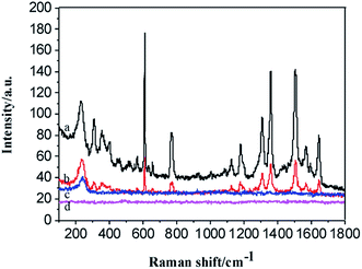 | ||
| Fig. 3 SERS spectra of R6G (10−6 M) in microfluidic SERS chips fabricated with different concentrations of PDDA: (a) 0.1%; (b) 0.3%; (c) 0.5%; (d) 1.0%. | ||
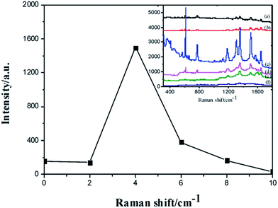
It is shown in Fig. 4a that the silver mirror film presented as an island film after the silver mirror reaction proceeded for 10 min. Before chemical plating, gold nanoparticles were evenly distributed on the surface of the Ag film (Fig. 4b). With increasing chemical plating time, the size of the AuNPs increased while the spacing between adjacent AuNPs decreased (Fig. 4c and d). For further clarification of the effect of chemical plating time on the SERS effect of the Ag film@nanoAu substrate, Raman spectra were collected using 10−5 M R6G as the probe molecule. The Raman intensity of C–C stretching of R6G at 1507 cm−1 was selected for analysing the effect of the surface morphology of the substrate on the SERS effect. As demonstrated in Fig. 5, a rapid increase in SERS intensity of C–C stretching of R6G was observed as the chemical plating time increased from 0 to 4 min. When the chemical plating time increased beyond 4 min, a rapid decrease in SERS intensity was observed. The results revealed that a chemical plating time of 4 min provided the highest Raman signal of R6G which might be attributed to the specific surface morphology of the substrate content of the Au nanoparticles with suitable size and interparticle distance on the Ag mirror film.
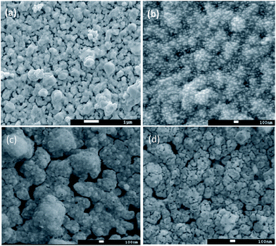 | ||
| Fig. 4 (a) SEM images of silver mirror film. SEM images of Ag film@nanoAu substrate with different chemical plating times of (b) 0 min, (c) 4 min, and (d) 10 min. | ||
Compared to single gold nanoparticles and a single silver mirror film, the SERS intensity of C–C stretching of R6G at 1507 cm−1 was calculated, showing that the SERS intensity of R6G on Ag film@nanoAu was improved by 4.6 and 3.6 times respectively (Fig. 6). The reason for this may be the production of two types of “hot spots” when the AuNPs adsorb onto the Ag film. One comes from the Au nanoparticles themselves, and the other one is those at the boundary between the AuNPs and the Ag film. The synergy of the two types of “hot spots” greatly improved the SERS effect of the Ag film@nanoAu substrate compared with the single metal SERS substrate. The finally derived microfluidic SERS chip with Ag film@nanoAu substrate was easy to fabricate, and could reduce contamination of the analyte and achieve a greatly enhanced Raman signal by utilizing the plasma synergy of gold and silver.
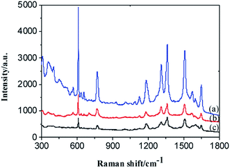 | ||
| Fig. 6 SERS spectra of R6G (10−5 M) in microfluidic SERS chips with (a) Ag film@nanoAu, (b) AuNPs substrate, and (c) Ag mirror film as SERS substrate, respectively. | ||
3.2 Evaluation of the efficiency of the microfluidic SERS chip
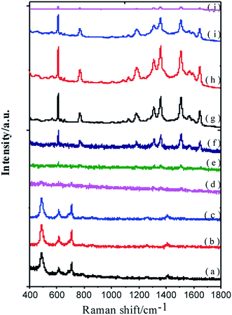
The greatest enhancement was found in the few nanometers closest to the substrate surface.36 Therefore, the laser focus position along the vertical direction was important for obtaining an optimized SERS signal. With the movement of the focus position from up to down, the SERS signal of the PDMS cover disappeared gradually, while the SERS signal of R6G appeared gradually (Fig. 7d). When the focus point was at the interface of the Ag film@nanoAu substrate and the sample, the strongest SERS signal of R6G was received (Fig. 7h), and the SERS signal of PDMS was not obvious and would not interfere with the signal of the analyte. Additionally, the closer the position was to the optimized focus point, the stronger the SERS signals of R6G would be. This was because the maximum SERS enhancing region decreased extremely rapidly with distance, and the interface might be the best position where the electromagnetic field generated by the system was strongest, so the strongest SERS signal of the analyte was derived.If the laser penetrated the cover plates of the chip to reach the analyte, the cover plates would weaken the laser power due to their optical absorption and scattering effects and finally decrease the SERS signal intensity of the analyte. Different materials produced different extents of optical absorption and scattering. PDMS and glass both with a thickness of 1 mm were used as cover plates of the same chip for SERS testing of R6G (Fig. 8). The SERS intensity of R6G at 1507 cm−1 decreased by 2.5 and 2.1 times respectively. PDMS was easy to punch to form a liquid storage pool, as well as to flexibly adjust the cover plate thickness. So PDMS was the ideal material for the cover plate in our experiment.
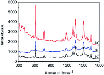 | ||
| Fig. 8 SERS spectra of R6G (10−5 M) in the same microfluidic SERS chip with different cover plates: (a) no cap, (b) PDMS, and (c) glass. | ||
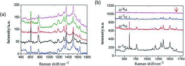
Reproducibility and sensitivity were two important indexes to evaluate the microfluidic SERS chips. The SERS signals of R6G obtained in 5 different microfluidic SERS chips fabricated under the same conditions were used to characterize the reproducibility of the Ag film@nanoAu substrate. It is shown in Fig. 9a that all of the spectra intensities of R6G were distributed in a narrow range. And the RSD of the peaks at 1507 cm−1 was calculated as 10.36%, which indicated that the fabrication method was of good reproducibility. For sensitivity characterization, different concentrations of R6G solution were used, as shown in Fig. 9b. With decreasing concentration of R6G, the signal intensity decreased. Although the SERS signal of R6G was decreased 2.1 times under the influence of the 1 mm PDMS cover plate, the peak at 1507 cm−1 could still be seen when the concentration of R6G was 10−8 M. These results demonstrated that the self-designed “sandwich” microfluidic SERS chip can meet the requirement of high sensitivity detection.
Additionally, the enhancement factor (EF) was used to characterize the SERS enhancement of the substrate. It was calculated as Leem described.25 To determine the EF, aqueous solutions of R6G with two different concentrations were prepared for the SERS and normal Raman measurements; the normal Raman signal was obtained from a 10−2 M R6G solution in a microfluidic chip with no SERS substrate and the SERS signal was obtained from a 10−8 M R6G solution in a microfluidic chip with the Ag film@nanoAu as the SERS substrate. An EF value for the Raman intensity at 1507 cm−1 was calculated as 3.8 × 10⁵.
4. Conclusion
Based on the excellent plasma characteristics of gold and silver, a new type of SERS substrate of Ag film@nanoAu was designed and fabricated in situ in a designed “sandwich” microfluidic chip by self-assembly-chemical plating. Meanwhile, the microfluidic SERS chip with Ag film@nanoAu as SERS substrate was constructed. The optimized SERS enhancing effect was observed when the focus point for detection was at the interface of the Ag film@nanoAu substrate and the sample in the microfluidic SERS chip. Compared to single silver or gold SERS substrate, the SERS intensity of the C–C vibration of the R6G molecule at 1507 cm−1 in the as-prepared microfluidic SERS chip with Ag film@nanoAu substrate was improved 4.6 and 3.6 times respectively because of the synergistic effect of gold and silver. The designed microfluidic SERS chip showed a better response with enhancement factors in the order of 3.8 × 10⁵ and a detection limit of 10−8 M, as well as high signal reproducibility with a RSD of 10.36% which was measured by probing an aqueous solution of R6G.Acknowledgements
The authors would like to thank Xue-Qiang Qi for assistance in the SERS detection. The work was financially supported by the National Natural Science Foundation of China (No. 21375156); the National High Technology Research and Development Program of China (863 Projects) (No. 2015AA021104 and No. 2015AA021107); Frontier Research Key Projects of Chongqing Science and Technology Committee (cstc2015jcyjBX0010) and Scientific and Technical Innovation Projects for People’s Livelihood of Chongqing Science and Technology Committee (cstc2015shms zx0014).References
- Á. Ríos, M. Zougagh and M. Avila, Anal. Chim. Acta, 2012, 740, 1–11 CrossRef PubMed.
- L. Chen and J. Choo, Electrophoresis, 2008, 29(9), 1815–1828 CrossRef CAS PubMed.
- A. F. Chrimes, K. Khoshmanesh, P. R. Stoddart, A. Mitchell and K. Kalantar-Zadeh, Chem. Soc. Rev., 2013, 42(13), 5880–5906 RSC.
- X. M. Lin, Y. Cui, Y. H. Xu, B. Ren and Z. Q. Tian, Anal. Bioanal. Chem., 2009, 394(7), 1729–1745 CrossRef CAS PubMed.
- M. Fan, G. F. Andrade and A. G. Brolo, Anal. Chim. Acta, 2011, 693(1–2), 7–25 CrossRef CAS PubMed.
- S. Pahlow, A. März, B. Seise, K. Hartmann, I. Freitag, E. Kämmer, R. Böhme, V. Deckert, K. Weber, D. Cialla and J. Popp, Eng. Life Sci., 2012, 12(2), 131–143 CrossRef CAS.
- J.-A. Huang, Y.-L. Zhang, H. Ding and H.-B. Sun, Adv. Opt. Mater., 2015, 3(5), 618–633 CrossRef CAS.
- M. Jahn, S. Patze, T. Bocklitz, K. Weber, D. Cialla-May and J. Popp, Anal. Chim. Acta, 2015, 860, 43–50 CrossRef CAS PubMed.
- H. Mao, W. Wu, Y. Zhang, P. Lv, C. Qian, J. Xu and H. Zhang, in Micro Electro Mechanical Systems (MEMS), 2011 IEEE 24th International Conference on, IEEE, 2011 Search PubMed.
- I. M. White, S. H. Yazdi and W. W. Yu, Microfluid. Nanofluid., 2012, 13(2), 205–216 CrossRef CAS.
- H.-Y. Fu, X.-Y. Lang, C. Hou, Z. Wen, Y.-F. Zhu, M. Zhao, J.-C. Li, W.-T. Zheng, Y.-B. Liu and Q. Jiang, J. Mater. Chem. C, 2014, 2(35), 7216–7222 RSC.
- Y. Deng, M. N. Idso, D. D. Galvan and Q. Yu, Anal. Chim. Acta, 2015, 863, 41–48 CrossRef CAS PubMed.
- Y. Zheng and T. Huang, Journal of the Association for Laboratory Automation, 2008, 13(4), 215–226 CrossRef CAS.
- B.-B. Xu, R. Zhang, X.-Q. Liu, H. Wang, Y.-L. Zhang, H.-B. Jiang, L. Wang, Z.-C. Ma, J.-F. Ku, F.-S. Xiao and H.-B. Sun, Chem Commun., 2012, 48(11), 1680–1682 RSC.
- Z. Geng, W. Liu, X. Wang and F. Yang, Sens. Actuators, A, 2011, 169(1), 37–42 CrossRef CAS.
- B.-B. Xu, Z.-C. Ma, L. Wang, R. Zhang, Li-G. Niu, Z. Yang, Y.-L. Zhang, W.-H. Zheng, B. Zhao, Y. Xu, Qi-D. Chen, H. Xia and H.-B. Sun, Lab Chip, 2011, 11(19), 3347–3351 RSC.
- G. L. Liu and L. P. Lee, Appl. Phys. Lett., 2005, 87(7), 074101 CrossRef.
- Y. L. Deng and Y. J. Juang, Biomicrofluidics, 2013, 7(1), 14111 CrossRef PubMed.
- M. Li, F. Zhao, J. Zeng, J. Qi, J. Lu and W.-C. Shih, J. Biomed. Opt., 2014, 19(11), 111611 CrossRef PubMed.
- B. B. Xu, Z. C. Ma, H. Wang, X. Q. Liu, Y. L. Zhang, X. L. Zhang, R. Zhang, H. B. Jiang and H. B. Sun, Electrophoresis, 2011, 32(23), 3378–3384 CrossRef CAS PubMed.
- Y. J. Oh and K. H. Jeong, Lab Chip, 2014, 14(5), 865–868 RSC.
- C. Farcau, N. M. Sangeetha, N. Decorde, S. Astilean and L. Ressier, Nanoscale, 2012, 4(24), 7870–7877 RSC.
- R. Takahashi, T. Fukuoka, Y. Utsumi and A. Yamaguchi, in Nano/Micro Engineered and Molecular Systems (NEMS), 2013 8th IEEE International Conference on, IEEE, 2013 Search PubMed.
- J. Parisi, L. Su and Y. Lei, Lab Chip, 2013, 13(8), 1501–1508 RSC.
- J. Leem, H. W. Kang, S. H. Ko and H. J. Sung, Nanoscale, 2014, 6(5), 2895–2901 RSC.
- R. A. Alvarez-Puebla, J. P. Bravo-Vasquez, P. Cheben, D. X. Xu, P. Waldron and H. Fenniri, J. Colloid Interface Sci., 2009, 333(1), 237–241 CrossRef CAS PubMed.
- M. Chen, I. Y. Phang, M. R. Lee, J. K. Yang and X. Y. Ling, Langmuir, 2013, 29(23), 7061–7069 CrossRef CAS PubMed.
- C. Wang, J. Fang, Y. Jin and M. Cheng, Appl. Surf. Sci., 2011, 258(3), 1144–1148 CrossRef CAS.
- J. Lee, B. Hua, S. Park, M. Ha, Y. Lee, Z. Fan and H. Ko, Nanoscale, 2014, 6(1), 616–623 RSC.
- M. Z. Si, Y. P. Kang and R. M. Liu, Appl. Surf. Sci., 2012, 258(15), 5533–5537 CrossRef CAS.
- A. Sivanesan, E. Witkowska, W. Adamkiewicz, L. Dziewit, A. Kaminska and J. Waluk, Analyst, 2014, 139(5), 1037–1043 RSC.
- G. Frens, Nature, 1972,(241), 20–22 Search PubMed.
- J. W. Chen, Study on Direct Writing Conductive Lines by Laser Induced Forward Transfer Technology in Physical Electronics, Huazhong University of Science & Technology, 2011 Search PubMed.
- L. Zhang, C. Wang and Y. Zhang, Appl. Surf. Sci., 2012, 258(14), 5312–5318 CrossRef CAS.
- D. Anderson and M. Moskovits, J. Phys. Chem. B, 2006, 110(28), 13722–13727 CrossRef CAS PubMed.
- B. Sharma, R. R. Frontiera, A.-I. Henry, E. Ringe and R. P. Van Duyne, Mater. Today, 2012, 15(1–2), 16–25 CrossRef CAS.
| This journal is © The Royal Society of Chemistry 2016 |

