
 Open Access Article
 This Open Access Article is licensed under a Creative Commons Attribution-Non Commercial 3.0 Unported Licence
Simultaneous laser-based graphitization and microstructuring of bamboo for supercapacitors derived from renewable resources†
Rikuto Miyakoshi a,
Shuichiro Hayashia and
Mitsuhiro Terakawa*ab
a,
Shuichiro Hayashia and
Mitsuhiro Terakawa*ab
aSchool of Integrated Design Engineering, Keio University, Yokohama, Kanagawa 223-8522, Japan. E-mail: terakawa@elec.keio.ac.jp
bDepartment of Electronics and Electrical Engineering, Keio University, Yokohama, Kanagawa 223-8522, Japan
First published on 17th October 2022
Abstract
Utilizing renewable resources for electrodes realizes the sustainable fabrication of a supercapacitor with high environmental friendliness. Laser-based graphitization of biomass has been emerging as a promising technique for patterning the electrodes of a supercapacitor with renewable resources. Herein, simultaneous patterning and microstructuring of laser-induced graphene (LIG) on a renewable biomass resource, bamboo, by a laser-based graphitization technique was demonstrated. By irradiating femtosecond laser pulses onto bamboo, graphitization and microstructuring were both induced simultaneously, forming conductive structures with high surface area. Furthermore, LIG patterned on bamboo by our method was used as the electrodes of supercapacitors. NaCl was selected as the electrolyte for the fabrication of supercapacitors. The proposed method realizes the fabrication of environmentally-friendly supercapacitors comprised of all renewable biomass resources.
Introduction
Energy storage is essential for on-site energy use, which has become increasingly important in recent years. Among various energy storage devices, much research is focused on supercapacitors because of their high capacitance. A supercapacitor consists of an electrolyte and electrodes made of conductive materials such as graphitic carbon.1–3 Utilization of renewable resources for the electrodes will realize the sustainable fabrication of supercapacitors with high environmental friendliness. Biomass, as one of the promising renewable resources, can be used as the precursor of graphitic carbon electrodes. Previously, the electrodes of supercapacitors were fabricated by the graphitization of bamboo, which is an abundant biomass resource because of its fast growth rate.4 For example, Gong et al. graphitized bamboo in a furnace using a non-toxic catalyst to fabricate the electrodes of supercapacitors.5Laser-based graphitization has become one of the most promising techniques for the single-step patterning of graphitic carbon. In 2014, Lin et al. revived the laser-based technique by reporting that the structures formed by laser irradiation onto polyimide were composed of graphitic carbon, referred to as laser-induced graphene (LIG).6 In addition to the synthetic polymers, LIG has been derived from natural resources, including silk,7 coconut,8 and wood.9 There have also been several reports on the application of biomass-derived LIG to the electrodes of supercapacitors.3,10 For example, Ye et al. used LIG derived from wood as electrodes of supercapacitors.3 It should be noted that the surface morphology of the electrode is crucial since the capacitance depends on the surface area of the electrode. Clarifying the relationship between the laser irradiation condition and the surface morphology of the patterned structure contributes to the patterning of the electrode with a high surface area, resulting in a high capacitance.
In this study, simultaneous patterning and microstructuring of LIG on a renewable biomass resource, bamboo, and the application of LIG as the electrodes of supercapacitors were demonstrated. Femtosecond laser pulses were irradiated onto bamboo to pattern electrically conductive structures composed of graphitic carbon and the laser-based graphitization of bamboo was demonstrated. Moreover, the surface morphologies of the patterned structures are discussed based on the porosity and surface roughness observed from the patterned structures. First, the relationship between the laser irradiation conditions and the electrical conductivity of the patterned structure was investigated. Next, surface morphology was observed by scanning electron microscopy and confocal laser scanning microscopy. Furthermore, we demonstrated that LIG patterned on bamboo using our method can be used as the electrodes of supercapacitors. We selected NaCl as the electrolyte of the supercapacitor to achieve an environmentally friendly supercapacitor comprised of all renewable biomass resources.
Experimental
Patterning of structures on bamboo
Bamboo (provided by Takeroku Co., Ltd., Japan) was cut into the thickness of 2 mm (Fig. S1a†). The transverse section of the bamboo was placed on a cover glass with a thickness of 150 μm, as shown in Fig. S1b.† The brown-outer surface in Fig. S1a† is the epidermis of bamboo. All structures in this study were patterned by irradiating laser pulses with a central wavelength of 522 nm (second harmonic wave of a 1045 nm femtosecond laser) and a pulse width of 192 fs, at a 63 MHz repetition rate, and a laser power of 150 mW using a fs laser system (High Q-2, Spectra-Physics Inc., USA). The laser pulses were focused onto a transverse section of bamboo using an objective lens (MPLN20x, Olympus Corp., Japan) with a numerical aperture (NA) of 0.4. The laser pulses were either single or multiple scanned by using an automatic 3-axis (xyz) translation stage. The estimated degree of overlapping between a line structure and the adjacent structure was defined as an overlap.Characterizations of patterned structures
Resistances were measured by the two-probe method using a digital source meter (175 True RMS Digital Multimeter, Fluke Corp., USA). For the resistance measurements, gold electrodes were fabricated by ion sputtering on both ends of the structures patterned on bamboo. The conductivity of the gold electrode was measured to be 4.4 S m−1. The dimensions and the surface morphologies of patterned structures were observed by a digital microscope (MS-100, Asahikogaku Co., Ltd., Japan) and a scanning electron microscope (SEM, SU-70, Hitachi High-Tech Corp., Japan), respectively. The width of the structures was defined as the width of the black-colored structures. The surface areas of the patterned structures were measured by a confocal laser scanning microscope (CLSM, VK-X1000, Keyence Corp., Japan). The chemical analysis of the patterned structure was conducted using a Fourier transfer infrared (FT-IR) spectrometer (ALPHA-E, Bruker Corp., USA) in attenuated total reflection mode, X-ray diffraction (XRD) spectrometer (D8 Discover, Bruker Corp., USA), and Raman spectrometer (InVia Raman Microscope, Renishaw Inc., UK). For the Raman analysis, an excitation wavelength of 532 nm was used, and the spectrum was recorded for a wave number of 1000–3000 cm−1.Characterizations of the supercapacitors using the patterned structures
The patterned structures were covered with agarose hydrogel containing NaCl to fabricate supercapacitors. The mixture of agarose (1.0%, w/v, Sigma-Aldrich Co. LLC, USA) and NaCl (5.8%, w/v, Sigma-Aldrich Co. LLC, USA) were heated at 80 °C for 30 minutes and then cooled at room temperature, according to a previously reported method.11 A digital source meter (175 True RMS Digital Multimeter, Fluke Corp., USA) was used to measure the capacitances of the supercapacitors. Potentiostat (Gamry 1010 Interface, Gamry Instruments Inc., USA) was used to obtain the cyclic voltammetry (CV) curve and galvanostatic charge–discharge (GCD) curve. The volumetric and areal capacitance were calculated based on the capacitance calculated from the CV curve, and the weight and the surface area of graphitic carbon electrodes. The areal energy density was calculated based on the GCD curve. Red LEDs (SLI-570UT, Rohm Co., Ltd., Japan) with a forward voltage of 1.9 V were connected to the supercapacitors charged with 6 V alkaline batteries for 1 minute.Results and discussion
A 6 mm-line structure was patterned on the surface of bamboo by single scanning of laser pulses. The surface of the bamboo (Fig. 1a) was visibly modified into a black-colored structure (Fig. 1b). The width of the black-colored structure was 140 μm, which is wider than the estimated spot diameter (1.6 μm). This is attributable to the thermal diffusion, which results from the accumulation of thermal energy induced by the absorption of high repetition rate (63 MHz) laser pulses. FT-IR spectra obtained from native bamboo and the patterned structure show that the intensities of the peaks corresponding to the O–H (3392 cm−1), CH2 (2933 cm−1), C–H (2900 cm−1), C–O (1058 cm−1), and C–O–C (1030 cm−1) lowered after laser irradiation (Fig. S2†). Additionally, the spectrum obtained from the patterned structure shows the peak corresponding to C![[double bond, length as m-dash]](https://www.rsc.org/images/entities/char_e001.gif) C (1566 cm−1), suggesting the formation of carbon structures. The XRD spectra obtained are insufficient to indicate the formation of graphitic carbon (Fig. S3†), since the diffraction peak observed around 25° can originate from both graphitic carbon as well as cellulose of native bamboo.12 On the other hand, the spectrum obtained from the Raman analysis performed at the center of the patterned structure shows three prominent peaks at 1350, 1600, and 2700 cm−1 (Fig. 1c). These peaks correspond to the D, G, and 2D bands, respectively, indicating the formation of graphitic carbon, such as LIG.13 Note that, bamboo is primarily comprised of crosslinked structure of cellulose, hemicellulose, and lignin, which is widely referred to as lignocellulose structure. Since lignin contains aromatic carbon, graphitic structures were probably formed by the thermal degradation of bamboo into carbon rich materials followed by the rearrangement of aromatic carbon, as similar to the discussion on formation mechanism of LIG from polyimide.6 The peak intensity ratio of the D and G bands (ID/IG), which has been used for evaluating the crystallinity of graphitic carbon, was 0.7. This value is within the range of those reported for LIG derived from synthetic and natural materials, including polyimide and cellulose nanofiber.14–16 However, no conductivity was confirmed via the two-probe method for the structures patterned in this study by single laser scanning.
C (1566 cm−1), suggesting the formation of carbon structures. The XRD spectra obtained are insufficient to indicate the formation of graphitic carbon (Fig. S3†), since the diffraction peak observed around 25° can originate from both graphitic carbon as well as cellulose of native bamboo.12 On the other hand, the spectrum obtained from the Raman analysis performed at the center of the patterned structure shows three prominent peaks at 1350, 1600, and 2700 cm−1 (Fig. 1c). These peaks correspond to the D, G, and 2D bands, respectively, indicating the formation of graphitic carbon, such as LIG.13 Note that, bamboo is primarily comprised of crosslinked structure of cellulose, hemicellulose, and lignin, which is widely referred to as lignocellulose structure. Since lignin contains aromatic carbon, graphitic structures were probably formed by the thermal degradation of bamboo into carbon rich materials followed by the rearrangement of aromatic carbon, as similar to the discussion on formation mechanism of LIG from polyimide.6 The peak intensity ratio of the D and G bands (ID/IG), which has been used for evaluating the crystallinity of graphitic carbon, was 0.7. This value is within the range of those reported for LIG derived from synthetic and natural materials, including polyimide and cellulose nanofiber.14–16 However, no conductivity was confirmed via the two-probe method for the structures patterned in this study by single laser scanning.
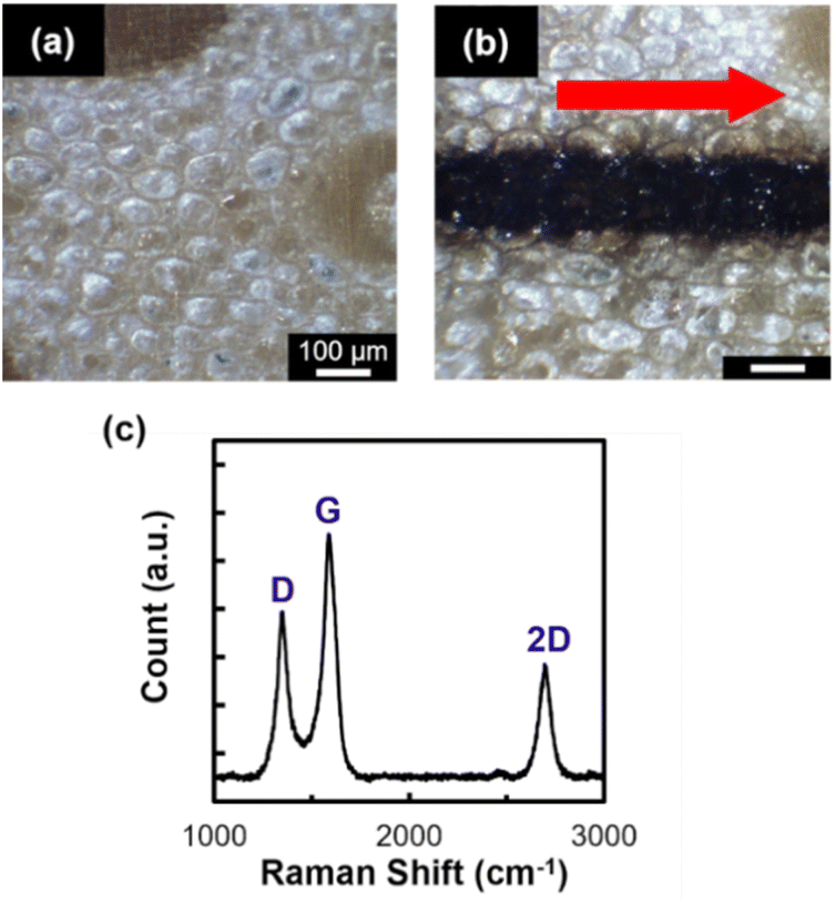 | ||
| Fig. 1 Digital microscope images of the bamboo (a) without and (b) with laser irradiation. The red arrow in (b) indicates the laser scanning direction. (c) Raman spectrum obtained from the structure. The structure was patterned with a laser scan speed of 1.00 mm s−1. The scale bars indicate 100 μm. | ||
Next, 6 mm structures were patterned by raster scanning of laser pulses as illustrated in Fig. 2a. The distance between adjacent scans was 35 μm, in which the overlap of laser scanning was 75%. Fig. 2b shows the relationship between the width (black) and conductance (blue) of the patterned structure and the number of laser scans used for patterning. The width, as well as the conductance, of the structure increased with the increase in the number of laser scans. Note that electrical conductivity was confirmed from structures patterned with 3 or more laser scans. The widths of the structures patterned with 3 or more laser scans were measured to be greater than 250 μm. Considering that the widths of native bamboo channels were 200 μm (Fig. S4†), it is suggested that the structures wider than such channels formed continuously with 3 or more laser scans.
 | ||
| Fig. 2 (a) Diagram showing the trajectory of raster laser scanning. (b) The relationships between the width (black) and conductance (blue) of the patterned structure and the number of laser scans used for patterning. The structures were patterned with a laser scan speed of 1.00 mm s−1. | ||
Fig. 3a shows the relationship between conductance of the structure and the laser scan speed used for patterning. The distance between adjacent scans and the number of laser scans were adjusted to keep a 75% overlap and 500 μm width, since the widths of the structures increased as the laser scan speed decreased (Fig. S5†). The conductance of the structure increased with an increase in laser scan speeds of 0.125–1.00 mm s−1. With a further increase in laser scan speed (i.e., 1.00–2.00 mm s−1), conductance of the structure decreased with an increase in laser scan speed. As the laser scan speed decreases, the number of irradiated pulses per spot increases. The maximum reached temperature may increase with the increase in total injected energy, leading to further graphitization.17 This may result in the increase in conductance with the decrease in laser scan speed. However, for excessively low laser scan speeds (i.e., 0.125–1.00 mm s−1), graphitic carbon may be decomposed due to significantly high maximum temperatures,18 which may result in the decrease in conductance with a decrease in laser scan speed.
 | ||
| Fig. 3 (a) The relationship between conductance of the structure and the laser scan speed used for patterning. (b–f) SEM images of the structures patterned with a laser scan speed of (b) 0.125, (c) 0.25, (d) 0.50, (e) 1.00, and (f) 2.00 mm s−1. The red double-headed arrow indicates the laser scanning direction. Macropore and micropore are indicated by the yellow and red circles, respectively. (g) The relationship between surface area of the structure and the laser scan speed used for patterning. All structures were patterned by raster laser scanning. The scale bars indicate 50 μm. | ||
SEM observations were conducted for structures patterned with different laser scan speeds (Fig. 3b–f). Micropores (red circle in Fig. 3f) with a diameter of 3 μm were observed for laser scan speeds of 0.125–2.00 mm s−1. In the case of laser-based graphitization, the material decomposition followed by gas release contributes to the formation of pores.6 In addition to the micropores, macropores (yellow circle in Fig. 3f) with a diameter of 50 μm were observed for laser scan speeds of 1.00 and 2.00 mm s−1. The diameters of macropores are comparable to that of bamboo's morphology (Fig. 1a). This suggests that the bamboo's morphology was inherited after laser irradiation with the laser scan speeds of 1.00 and 2.00 mm s−1. The inheritance of the morphology after processing is consistent with the case reported for the graphitization of wood in a furnace.19 For laser scan speeds of 0.125, 0.25, and 0.50 mm s−1, grooves were observed along the scanning direction of the laser pulses. It is speculated that the material was removed by laser ablation, which resulted in the formation of grooves and the microstructuring of graphitic carbon. Note that these grooves possess flake-like morphology (Fig. S6†). Although the exact mechanism of the formation of flake-like morphology has yet to be revealed, previous studies of LIG have discussed the effect of rapid gas release induced by laser irradiation.20,21 The relationship between surface area of the structure and laser scan speed used for patterning is shown in Fig. 3g. Surface area of the structure decreased with the increase in laser scan speed. It is speculated that the formation of grooves with flake-like morphology contributed to the high surface area, which resulted in higher surface areas measured for slower laser scan speeds.
Structures were patterned by two-step laser scanning, where laser pulses are first scanned in the horizontal direction, and then scanned in the vertical direction (Fig. 4a). This laser scanning is hereafter referred to as grid laser scanning. The SEM images of the structures patterned by grid laser scanning with different overlaps of 45, 60, 75, and 90% are shown in Fig. 4b–e, respectively. Conductivity was confirmed for the structures patterned by grid laser scanning with 45, 60, 75, and 90% overlaps (Fig. S7†). Similar to the results obtained for structures patterned by raster laser scanning (Fig. 3b–d), grooves were observed for the structures patterned with 45 (Fig. 4b), 60 (Fig. 4c), and 75% (Fig. 4d) overlaps. However, the grooves were not observed for the structures patterned with a 90% (Fig. 4e) overlap. Fig. S8a and b† show the CLSM images that indicate the height of the structures, obtained from the structures patterned with 75 and 90% overlaps, respectively. 0 μm indicates the height of the surface of non-irradiated bamboo, on which the side where laser pulses were focused. The height lower than 200 μm was measured in a width of 300 μm for structures patterned by grid laser scanning with a 90% overlap. Compared to the case for 75% overlap, excessive removal of the material was induced by laser ablation for 90% overlap. The relationship between the surface area of the patterned structure and the overlap is shown in Fig. 4f. The surface area of the structure increased with an increase in the overlap. Further ablation was induced with the subsequent scans, as well as the overlap of laser scanning. It is speculated that further ablation resultantly increased the surface area by forming flake-like morphology. Notably, in comparison with the surface area for the structure patterned by raster laser scanning with a 75% overlap (Fig. 3g), the surface area was 3 times higher for the structure patterned by grid laser scanning with a 75% overlap. Our technique realizes the significant increase in surface area of electrodes by the simple addition of laser scanning. Moreover, this technique may be applied to also increase the surface area of LIG electrodes derived from other biomasses.
 | ||
| Fig. 4 (a) Diagram showing the trajectory of grid laser scanning. SEM images of the structures patterned with (b) 45, (c) 60, (d) 75, and (e) 90% overlap. (f) Relationship between the surface area of the patterned structure and overlap of laser scanning. All structures were patterned by grid laser scanning with a laser scan speed of 0.25 mm s−1. The scale bars indicate 50 μm. | ||
To demonstrate the applicability of the patterned structures for supercapacitor fabrications, structures were used as electrodes of supercapacitors. Fig. 5a shows the schematic diagram of the supercapacitor. A pair of 6000 × 500 μm (length × width) structures were patterned by either raster laser scanning or grid laser scanning. Two structures were patterned with a distance of 100 μm apart. The patterned structures were then covered with an agarose hydrogel, containing NaCl. NaCl acted as an electrolyte, and the agarose hydrogel acted as an electrolyte retainer. NaCl and agarose were chosen since both materials are renewable and exhibit low environmental toxicity. The CV curve and GCD curve of the supercapacitor fabricated by using structures patterned by grid laser scanning with 75% overlap are shown in Fig. S9 and S10,† respectively. The pseudo-rectangular shape of CV curve and nearly triangular shape of GCD curve suggest the electrochemical double layer capacitor behaviour. Fig. 5b shows the relationship between the capacitance of the supercapacitor and the overlap of laser scanning used for the patterning of the electrodes. The measured capacitance was 23.1 μF for raster laser scanning with a 75% overlap, while the capacitance for grid laser scanning with a 75% overlap was 70.4 μF. The difference in capacitances is comparable to the difference in surface areas between the structures patterned by raster laser scanning and grid laser scanning with 75% overlap. The increase in surface area resulted in the increase in capacitance. The capacitance of the structure increased monotonically with an increase in overlap for the structures patterned by raster laser scanning, while the capacitance of the structure patterned by grid laser scanning reaches the peak of capacitance at 75%. The peak of capacitance confirmed at a 75% overlap for the structures patterned by grid laser scanning can be attributable to the significantly low conductance of the structure patterned with 90% overlap.
 | ||
| Fig. 5 (a) Schematic of the fabricated supercapacitor. (b) Capacitances of the supercapacitors using structures patterned by raster laser scanning and grid laser scanning with various overlaps of laser scanning. All structures were patterned with a laser scan speed of 0.25 mm s−1. | ||
A pair of comb-shaped structures, widely used to increase the surface area of the electrode,22,23 was patterned by either raster laser scanning or grid laser scanning, and then covered with an agarose hydrogel, containing NaCl (Fig. 6a). Fig. 6b shows a photograph of the fabricated supercapacitor. The capacitances measured for structures patterned by raster laser scanning and grid laser scanning were 95 and 290 μF, respectively. The volumetric and areal capacitance of the supercapacitor fabricated from the structures patterned by grid laser scanning were calculated to be 292.3 mF g−1 and 2.8 mF cm−2, respectively, from the CV curve (Fig. S11†). The areal energy density was calculated to be 0.3 μW h cm−2 from the GCD curve. In addition, the cycle stability test showed that the retention of the initial capacitance after 1000 cycles was ∼100% (Fig. S12†). The supercapacitor was charged using a battery and then connected to a LED to assess the discharge properties. Fig. 6c and d show the photographs at the indicated time interval of the red LED. The red light was confirmed for both supercapacitors fabricated by raster laser scanning and grid laser scanning at 0 s, which shows that the supercapacitor discharged to the LED. The brightness of the red light gradually decreased with elapse of time for 0–12 s. Note that the red light was only confirmed for LED connected to a supercapacitor using structure patterned by grid laser scanning at 12 s, which is attributable to the higher capacitance measured for the supercapacitor fabricated from the structure patterned by grid laser scanning. The proposed method realizes the rapid fabrication of environmentally-friendly supercapacitors from fully renewable biomass resources.
 | ||
| Fig. 6 (a) Schematic and (b) photograph of fabricated supercapacitor. (c and d) Photographs of LED at the indicated time interval. The LEDs were connected to supercapacitors using structures patterned by (c) raster laser scanning and (d) grid laser scanning. All structures were patterned with a laser scan speed of 0.25 mm s−1 and a 75% overlap of laser scanning. | ||
Conclusion
In conclusion, conductive LIG was patterned on bamboo by laser-based graphitization technique. The surface areas measured for the structures patterned by raster laser scanning increased with the decrease in laser scan speed, which is attributable to the formation of grooves with flake-like morphology. In comparison with the structure patterned by raster laser scanning, higher surface area was measured for the structure patterned by grid laser scanning. Conductive structures patterned by laser irradiation on bamboo were covered with agarose hydrogels containing NaCl to fabricate supercapacitors using renewable resources. The capacitance measured for the structures patterned by grid laser scanning was higher than that for structures patterned by raster laser scanning, which is explained by the higher surface area. When the supercapacitor was connected to the LED, light was observed for longer time for grid laser scanning, owing to the higher capacitance. The proposed method induces simultaneous graphitization and microstructuring of bamboo, realizing the fabrication of environmentally friendly supercapacitor comprised of all renewable biomass resources.Author contributions
Rikuto Miyakoshi: conceptualization, methodology, investigation, writing – original draft. Shuichiro Hayashi: conceptualization, methodology, writing – review & editing. Mitsuhiro Terakawa: conceptualization, project administration, supervision, funding acquisition, writing – review & editing.Conflicts of interest
There are no conflicts to declare.Acknowledgements
This work was partially supported by the Keio Gijuku Fukuzawa Memorial Fund for the Advancement of Education and Research, and a grant from TEPCO Memorial Foundation. Authors acknowledge Takeroku Co., Ltd., Japan for providing us bamboo materials.References
- Y. Wang, Z. Q. Shi, Y. Huang, Y. F. Ma, C. Y. Wang, M. M. Chen and Y. S. Chen, J. Phys. Chem. C, 2009, 113, 13103–13107 CrossRef CAS.
- Y. W. Zhu, S. Murali, M. D. Stoller, K. J. Ganesh, W. W. Cai, P. J. Ferreira, A. Pirkle, R. M. Wallace, K. A. Cychosz, M. Thommes, D. Su, E. A. Stach and R. S. Ruoff, Science, 2011, 332, 1537–1541 CrossRef CAS PubMed.
- R. Ye, Y. Chyan, J. Zhang, Y. Li, X. Han, C. Kittrell and J. M. Tour, Adv. Mater., 2017, 29, 1702211 CrossRef PubMed.
- Z. H. Li, C. J. Chen, R. Y. Mi, W. T. Gan, J. Q. Dai, M. L. Jiao, H. Xie, Y. G. Yao, S. L. Xiao and L. B. Hu, Adv. Mater., 2020, 32, 1906308 CrossRef CAS PubMed.
- Y. Gong, D. Li, C. Luo, Q. Fu and C. Pan, Green Chem., 2017, 19, 4132–4140 RSC.
- J. Lin, Z. Peng, Y. Liu, F. Ruiz-Zepeda, R. Ye, E. L. G. Samuel, M. J. Yacaman, B. I. Yakobson and J. M. Tour, Nat. Commun., 2014, 5, 5714 CrossRef CAS PubMed.
- Z. Li, L. Lu, Y. Xie, W. Wang, Z. Lin, B. Tang and N. Lin, Adv. Eng. Mater., 2021, 23, 2100195 CrossRef CAS.
- Y. Chyan, R. Ye, Y. Li, S. P. Singh, C. J. Arnusch and J. M. Tour, ACS Nano, 2018, 12, 2176–2183 CrossRef CAS PubMed.
- R. Trusovas, K. Ratautas, G. Račiukaitis and G. Niaura, Appl. Surf. Sci., 2019, 471, 154–161 CrossRef CAS.
- T. S. D. Le, S. Park, J. An, P. S. Lee and Y. J. Kim, Adv. Funct. Mater., 2019, 29, 1902771–1902780 CrossRef.
- W. G. Moon, G.-P. Kim, M. Lee, H. D. Song and J. Yi, ACS Appl. Mater. Interfaces, 2015, 7, 3503–3511 CrossRef CAS PubMed.
- J. Wei, C. Du, H. Liu, Y. Chen, H. Yu and Z. Zhou, Bioresources, 2016, 11, 8386–8395 CAS.
- A. C. Ferrari, Solid State Commun., 2007, 143, 47–57 CrossRef CAS.
- Z. Qin, X. Huang, D. Wang, T. He, Q. Wang and Y. Zhang, Surf. Interface Anal., 2000, 29, 514–518 CrossRef CAS.
- E. R. Mamleyev, S. Heissler, A. Nefedov, P. G. Weidler, N. Nordin, V. V. Kudryashov, K. Länge, N. MacKinnon and S. Sharma, npj Flexible Electron., 2019, 3, 2 CrossRef.
- F. Morosawa, S. Hayashi and M. Terakawa, ACS Sustainable Chem. Eng., 2021, 9, 2955–2961 CrossRef CAS.
- Y. Chen, J. Long, S. Zhou, D. Shi, Y. Huang, X. Chen, J. Gao, N. Zhao and C. P. Wong, Small Methods, 2019, 3, 1900208 CrossRef CAS.
- F. Liu, M. Wang, Y. Chen and J. Gao, J. Solid State Chem., 2019, 276, 100–103 CrossRef CAS.
- Y. Ma, D. Yao, H. Liang, J. Yin, Y. Xia, K. Zuo and Y.-P. Zeng, Electrochim. Acta, 2020, 352, 136452 CrossRef CAS.
- M. Abdulhafez, G. N. Tomaraei and M. Bedewy, ACS Appl. Nano Mater., 2021, 4, 2973–2986 CrossRef CAS.
- L. X. Duy, Z. Peng, Y. Li, J. Zhang, Y. Ji and J. M. Tour, Carbon, 2018, 126, 472–479 CrossRef CAS.
- J. Chmiola, C. Largeot, P.-L. Taberna, P. Simon and Y. Gogotsi, Science, 2010, 328, 480–483 CrossRef CAS PubMed.
- J. Ge, M. Zhu, E. Eisner, Y. Yin, H. Dong, D. D. Karnaushenko, D. Karnaushenko, F. Zhu, L. Ma and O. G. Schmidt, Small, 2021, 17, 2101704 CrossRef CAS PubMed.
Footnote |
| † Electronic supplementary information (ESI) available. See DOI: https://doi.org/10.1039/d2ra05641k |
| This journal is © The Royal Society of Chemistry 2022 |