
 Open Access Article
 This Open Access Article is licensed under a
 Creative Commons Attribution 3.0 Unported Licence
Rapid growth of fully-inorganic flexible CaxCoO2 thin films from a ligand free aqueous precursor ink for thermoelectric applications†
Tridib Kumar
Sinha
 ab,
Jinho
Lee
c,
Jin Kuk
Kim
b,
Samit K.
Ray
ad and
Biplab
Paul
*e
ab,
Jinho
Lee
c,
Jin Kuk
Kim
b,
Samit K.
Ray
ad and
Biplab
Paul
*e
aDepartment of Physics, Indian Institute of Technology, Kharagpur 721302, India
bDepartment of Materials Engineering and Convergence Technology, Gyeongsang National University, Jinju 52828, South Korea
cThe Research Institute of Natural Science and Department of Physics Education, Gyeongsang National University, Jinju 52828, South Korea
dS N Bose National Centre for Basic Sciences, Kolkata 700106, India
eThin Film Physics Division, Department of Physics, Chemistry, and Biology (IFM), Linköping University, SE-581 83 Linköping, Sweden. E-mail: biplab.paul@liu.se
First published on 7th June 2019
Abstract
We demonstrate a ligand-free green chemical method for the rapid growth of nanoporous Ca0.35CoO2 thin films on sapphire and mica substrates from a water-based precursor ink, formulated by dissolving the precursor solid, composed of in situ prepared Ca2+–DMF and Co2+–DMF complexes. Mica serves as the flexible substrate as well as the sacrificial layer for the film transfer. Despite the presence of nanopores, the power factor of the flexible film Ca0.35CoO2-on-mica is above 0.50 × 10⁻⁴ W m−1 K−2 at around room temperature. The present technique is simple and cost-effective.
Layered calcium cobaltates, e.g., CaxCoO2 and [Ca2CoO3]0.62CoO2 (also represented as Ca3Co4O9), because of their remarkable thermal and chemical stability and nontoxicity, have attracted significant interest for diverse applications, e.g. catalysis,1,2 batteries,3 supercapacitors,4 optoelectronics,5 and particularly for thermoelectrics.6–11 The thin films of this class of materials can be promising for flexible applications if film deposition is possible on flexible substrates or otherwise transferable onto flexible platforms. Although, CaxCoO2 thin films have been grown by physical deposition techniques,12,13 for scalability, chemical solution deposition (CSD) methods are often preferred over the physical methods. In particular, the CSD technique is cost-effective and facile.14–16 However, oxide materials are mostly insoluble, restricting their solution processability. For Ca3Co4O9, sol–gel chemical methods have been implemented, however the poor structural quality, arising from undesired cross-reactions or non-homogeneous precipitation limits its applicability.17,18 Panchakarla et al. reported the growth of misfit layered Ca3Co4O9 nanotubes by base-treatment of pre-formulated calcium cobalt oxide,19 but, because of the insolubility factor, the process seems to be complicated for the deposition of thin films.
There are some methods to formulate the thermoelectric inks but mostly with thermally unstable organic polymers.14 Because of the availability of suitable solvents, some chalcogenidometallate-based TE materials have been developed from the respective precursor inks,15 but with no such report on oxide materials. Recently, the growth of misfit layered cobaltate thin films has been accomplished using a water-based solution containing the co-ordination complex of metal ions with EDTA (ethylenediaminetetraacetic acid) and PEI (polyethyleneimine).20 However, the preparation of the complex-solution remains tedious, time consuming and moreover hazardous.21,22 Despite some investigations on the CSD growth of Ca3Co4O9, there is no report on the growth of CaxCoO2 by this route. The CaxCoO2 thin film, due to its higher power factor compared to Ca3Co4O9, is promising for near room temperature TE applications. The Ca0.33CoO2 thin film is reported to exhibit a high power factor of 0.9 mW m−1 K−2 at 300 K,23 which is several times higher than that of Ca3Co4O9,8–11 and remarkably higher than those of other layered cobaltates AxCoO2 [A = Sr, La, Pr, or Nd].6,7,24,25 For a high output power from a thermoelectric converter (TEC), its constituent active materials are required to have a high power factor.26 In fact, having a high power factor is more important than efficiency for a thin film based TEC with planar geometry, where heat flows in parallel to the film surface.27
Therefore, the development of alternative strategies to grow high performance and mechanically flexible CaxCoO2 thin films in a facile, cost-effective and environment-friendly process can offer a viable solution for low power requirements of emerging portable and wearable electronics. Here, we report the rapid growth of Ca0.35CoO2 thin films on sapphire and flexible mica substrates from a ligand-free aqueous TE precursor ink. The ink is a mixture of in situ prepared Ca2+–DMF and Co2+–DMF complexes. The fully-inorganic flexible Ca0.35CoO2-on-mica film, unlike organic and hybrid films, can sustain high temperature and thus be useful for applications in a wide temperature range: from room-temperature wearable applications (harvesting electrical power from body heat to power wearable electronics) to waste-heat recovery from hot surfaces of varying geometries (e.g., hot pipes).
Metal ions such as Ca2+, Co2+, etc. are very susceptible to complexation with polar solvents such as DMF.28–31 DMF is cheaper31 as well as less-hazardous32 and recyclable. The white precipitate of Ca2+–DMF and violet precipitate of Co2+–DMF were separately prepared, as shown in Fig. 1a, simply by dissolving the salts (i.e., Ca(CH3COO)2·H2O and Co(CH3COO)2·H2O) in a molar ratio of 3![[thin space (1/6-em)]](https://www.rsc.org/images/entities/char_2009.gif) :4 into an excess of hot DMF, followed by subsequent cooling at room temperature. The DMF forms complexes with the metal ions through its amide functionality (as schematically shown in Fig. 1a). A purple color precipitate was obtained by mixing the precipitates of Ca2+–DMF and Co2+–DMF, and re-precipitating from the hot DMF, as shown in Fig. 1b, which upon drying, produces a pink brown color precursor solid. This solid was easily dissolved in de-ionized (DI) water to obtain a stable homogenous solution of a bluish precursor ink (Fig. 1b). During the formation of DMF-complexes, there is a possibility of partial substitution of the acetate ions (–COOCH3−) by the DMF.
:4 into an excess of hot DMF, followed by subsequent cooling at room temperature. The DMF forms complexes with the metal ions through its amide functionality (as schematically shown in Fig. 1a). A purple color precipitate was obtained by mixing the precipitates of Ca2+–DMF and Co2+–DMF, and re-precipitating from the hot DMF, as shown in Fig. 1b, which upon drying, produces a pink brown color precursor solid. This solid was easily dissolved in de-ionized (DI) water to obtain a stable homogenous solution of a bluish precursor ink (Fig. 1b). During the formation of DMF-complexes, there is a possibility of partial substitution of the acetate ions (–COOCH3−) by the DMF.
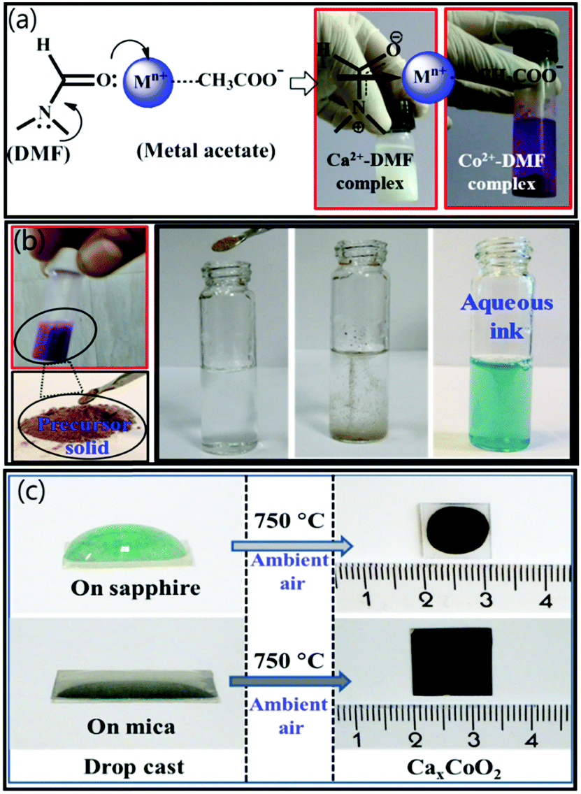 | ||
| Fig. 1 (a) Formation of the Ca2+–DMF and Co2+–DMF complexes as white and violet precipitates, respectively. (b) Formation of a pink brown precursor solid and the preparation of an aqueous TE ink, (c) the Ca0.35CoO2 thin film on the sapphire and mica substrates, grown by drop casting the ink followed by annealing at 700 °C in air. | ||
The DMF-complexes are likely to behave as zwitterions. During the mixing of the DMF-complexes, the zwitterions electrostatically interact with each other, and form the precipitate of the complex-conjugates, which was dried to obtain the pink brown precursor solid. The solid is likely to be soluble in polar solvents because of its abundant ionic characteristics. Water, being the most environmentally friendly polar solvent, here, we have demonstrated the formulation of a stable (stability was noticed for 60 days) aqueous precursor ink for TE application. The ink (containing a solid content of 10 mg mL−1) was drop-casted on sapphire and mica substrates, as shown in Fig. 1c. The muscovite mica, because of its inherently layered structure, where aluminosilicate layers are loosely bound by the boundary layer of potassium (K+) ions, can serve as the flexible substrate.33
After heat treatment at 700 °C for 10 min under an ambient atmosphere, the precursor solution turned into dark films of Ca0.35CoO2. The film on the mica substrate, unlike that on the sapphire substrate, was uniform. This is because, the angle of contact between the solution and hydrophilic mica34 is much smaller than that of sapphire, which results in uniform spreading of the solution over the mica substrate.
During the mixing of the DMF-complexes under vigorous stirring, the Co2+–DMF complex (because of its smaller size) occupies the interstitial spaces of Ca2+–DMF through the favorable electrostatic interaction among the active groups in the periphery of the metal ions, resulting in an in situ electrically and stoichiometrically balanced thermoelectric precursor solid (i.e., Ca2+/Co2+–DMF mixed complex). During heat treatment, the coordinated DMF reduces the Co2+ nanoparticles to Co0 nanoparticles, which in the presence of abundant oxygen transform to CoO2.35,36 The plausible reaction mechanism is shown in Scheme S1 (ESI†). The DMF degrades at high temperature, producing H2O, CO2, N2, NOx, etc., resulting in porosity in the films. Ca2+–DMF is ionized at high temperature and forms Ca0.35CoO2.
Fig. 2a and b show the XRD scans of the films Ca0.35CoO2-on-mica and Ca0.35CoO2-on-sapphire, respectively. Both the figures show Ca0.35CoO2 001 and 002 peaks. The peaks from no other planes, except the (00l) planes of Ca0.35CoO2, indicate the c-axis orientation of both the films. Apart from Ca0.35CoO2, the peaks from the mica and sapphire substrates are also visible as shown in Fig. 2a and b, respectively. The d-spacing for both the films is calculated to be 5.437 Å, which nearly matches with the value reported elsewhere.37
 | ||
| Fig. 2 XRD patterns of the films (a) Ca0.35CoO2-on-mica and (b) Ca0.35CoO2-on-sapphire. | ||
Fig. 3a shows a typical SEM image of Ca0.35CoO2-on-sapphire. A random distribution of the triangular grains of Ca0.35CoO2 is visible in Fig. 3a. The presence of nanopores in the film is indicated by the white open circles. Fig. 3b shows the magnified SEM image. The inset of Fig. 3b shows the polygonal shape of some fine grains of Ca0.35CoO2 of dimension less than 200 nm. Fig. 3c shows a typical SEM image of Ca0.35CoO2-on-mica, where the random distribution of nanopores of irregular shapes is clearly visible. A relatively smooth surface and the absence of any larger grains above 200 nm are evident from the magnified SEM image (Fig. 3d). The inset of Fig. 3d shows the polygonal shape of the grains of Ca0.35CoO2. The seemingly flat surface of both the films is attributed to the out-of-plane orientation of the films, which is consistent with the XRD observation. The growth of oriented films on both the substrates is intrinsically attributed to the effect of self-assembly during annealing, where the driving force is the external stress due to solvent evaporation.38 The higher porosity of Ca0.35CoO2-on-mica compared to Ca0.35CoO2-on-sapphire might be due to the slow evaporation of the surface absorbed water in the more hygroscopic mica during the formation of the film.39 From the above study, it is conjectured that the present CSD method can be applicable to grow Ca0.35CoO2 thin films on arbitrary substrates, which sustain a high annealing temperature of 700 °C. The porosity of the films can also be controlled by preferential selection of the substrate with the desired hygroscopic properties.
 | ||
| Fig. 3 (a) SEM image of Ca0.35CoO2-on-sapphire. (b) Magnified image of a small portion of the Ca0.35CoO2-on-sapphire film; and the inset shows the polygonal shape of the grains in the film. (c) SEM image of Ca0.35CoO2-on-mica. (d) Magnified image of a small portion of the Ca0.35CoO2-on-mica film; and the inset shows the polygonal shape of the fine grains in the film. | ||
Fig. 4a shows a typical optical image of the bent Ca0.35CoO2 film of thickness ∼300 nm on the mica substrate (25 μm thickness). The film is bendable to a bending radius of 15 mm without developing any cracks, as confirmed by optical microscopy. As shown in Fig. 4b, the transferability of the film is demonstrated by transferring the film from the parent mica substrate onto a sticky tape.
 | ||
| Fig. 4 (a) Image of thin flexible Ca0.35CoO2-on-mica film. (b) Demonstration of the film transfer onto sticky tape. | ||
Fig. 5a shows the temperature dependent electrical resistivity of Ca0.35CoO2-on-sapphire (red circles) and Ca0.35CoO2-on-mica (black open circles). The room temperature resistivity values are 15.6 and 14.6 mΩ cm for Ca0.35CoO2-on-sapphire and Ca0.35CoO2-on-mica, respectively, which are higher than the values for Ca0.35CoO2 reported elsewhere,12,40 however, comparable to that of undoped Ca3Co4O9 thin films.41,42 Even with a nanoporous structure, the low electrical resistivity of Ca0.35CoO2-on-mica is attributed to its better crystalline quality than the film Ca0.35CoO2-on-sapphire. From this, it is apparent that the nanopores do not act as the scattering centre for the charge carriers, which might be due to the greater interpore separation compared to the electron mean free path. However, the thermal conductivity of the film is anticipated to be reduced, due to the enhanced scattering of phonons by the nanopores. This anticipation is due to the fact that the phonon mean free path is one order of magnitude higher than the electron mean free path, and by controlling the characteristic length scale of the nanoporous structure within the range of electron and phonon mean free paths, the phonons can be selectively scattered, but without hampering the electronic transport.43,44Fig. 5b shows the temperature dependent Seebeck coefficient of the films. The room temperature Seebeck coefficient values are 78 and 88 μV K−1 for the Ca0.35CoO2-on-sapphire and Ca0.35CoO2-on-mica films, respectively, which are comparable to the value reported for single crystalline Ca0.33CoO2,30 however, sufficiently higher than those of sputter deposited CaxCoO2 thin films reported elsewhere.15 The Seebeck coefficient varies with temperature in a similar manner to the electrical resistivity. Fig. 5c shows the temperature dependent power factor of the films. The room temperature power factor values are 0.39 and 0.50 × 10⁻⁴ W m−1 K−2 for the films Ca0.35CoO2-on-sapphire and Ca0.35CoO2-on-mica, respectively, which are interestingly comparable to the reported values for undoped Ca3Co4O9 thin films.41,42 The slightly higher power factor of the film Ca0.35CoO2-on-mica compared to that of the Ca0.35CoO2-on-sapphire film is attributed to the lower electrical resistivity of the former than the latter.
 | ||
| Fig. 5 Temperature dependent (a) electrical resistivity, (b) Seebeck coefficient, and (c) power factor of the films Ca0.35CoO2-on-mica and Ca0.35CoO2-on-sapphire. | ||
The film Ca0.35CoO2-on-mica can be useful for flexible applications in a wide temperature range, from room temperature to a few hundred degrees above room temperature, due to its high power factor, above 0.50 × 10⁻⁴ W m−1 K−2 until 300 °C. To investigate the effect of bending stress on the TE performance, the Ca0.35CoO2-on-mica film was subjected to 100 times of bending, and then TE measurements were performed. No notable changes in the Seebeck coefficient and electrical resistivity values were found; and any small variations in the values are within the error limit specified for the measuring instrument. It is noteworthy that the present films are undoped and a further improvement of the power factor is still possible upon doping.
The present thin film growth technique from the thermoelectric precursor ink, being simple, eco-friendly and less time consuming, is potentially suitable for industrial upscaling.
This research was supported by the Science and Engineering Research Board (SERB/1759/2014-15), the DST “GPU”, Government of India, Basic Science Research Program through the National Research Foundation of Korea (NRF) funded by the Ministry of Education (2016R1D1A1B03931391), and through funding from the Åforsk foundation (Grant No. 17-578). P. Eklund (Linköping University) is acknowledged for his critical reading of the manuscript and additional funding through the Swedish Government Strategic Research Area in Materials Science on Functional Materials at Linköping University (Faculty Grant SFO-Mat-LiU No. 2009 00971).
Conflicts of interest
There are no conflicts to declare.References
- C. Dang, Y. Li, S. M. Yusuf, Y. Cao, H. Wang, H. Yu, F. Peng and F. Li, Energy Environ. Sci., 2018, 11(3), 660–668 RSC.
- C. S. Lim, C. K. Chua, Z. Sofer, O. Jankovsky and M. Pumera, Chem. Mater., 2014, 26(14), 4130–4136 CrossRef CAS.
- D. W. Kim, Y. D. Ko, J. G. Park and B. K. Kim, Angew. Chem., 2007, 46(35), 6654–6657 CrossRef CAS PubMed.
- Z. Wang, Y. Wang, X. Yue, G. Shi, M. Shang, Y. Zhang, Z. Lv and G. Ao, J. Alloys Compd., 2019, 792, 357–364 CrossRef CAS.
- L. Lajaunie, A. Ramasubramaniam, L. S. Panchakarla and R. Arenal, Appl. Phys. Lett., 2018, 113(3), 031102 CrossRef.
- G. G. Yadav, A. David, T. Favaloro, H. Yang, A. Shakouri, J. Caruthers and Y. Wu, J. Mater. Chem. A, 2013, 1(38), 11901–11908 RSC.
- V. Thoréton, Y. Hu, C. Pirovano, E. Capoen, N. Nuns, A. S. Mamede, G. Dezanneau, C. Y. Yoo, H. J. M. Bouwmeesterc and R. N. Vannier, J. Mater. Chem. A, 2014, 2(46), 19717–19725 RSC.
- B. Paul, J. L. Schroeder, S. Kerdsongpanya, N. V. Nong, N. Schell, D. Ostach, J. Lu, J. Birch and P. Eklund, Adv. Electron. Mater., 2015, 1, 1400022 CrossRef.
- B. Paul, J. Lu and P. Eklund, ACS Appl. Mater. Interfaces, 2017, 9, 25308–25316 CrossRef CAS PubMed.
- B. Paul, E. M. Björk, A. Kumar, J. Lu and P. Eklund, ACS Appl. Energy Mater., 2018, 1, 2261–2268 CrossRef CAS PubMed.
- Y. Du, J. Xu, B. Paul and P. Eklund, Appl Mater Today, 2018, 12, 366–388 CrossRef.
- T. Kanno, S. Yotsuhashi and H. Adachi, Appl. Phys. Lett., 2004, 85, 739 CrossRef CAS.
- B. Paul, J. Lu and P. Eklund, Nanomaterials, 2019, 3, 443 CrossRef PubMed.
- S. Jo, S. Choo, F. Kim, S. H. Heo and J. S. Son, Adv. Mater., 2018, 1804930 Search PubMed.
- Z. Wang, Y. Ma, P. B. Vartak and R. Y. Wang, Chem. Commun., 2018, 54(65), 9055–9058 RSC.
- A. L. Tiano, C. Koenigsmann, A. C. Santulli and S. S. Wong, Chem. Commun., 2010, 46(43), 8093–8130 RSC.
- R. Wei, X. Tang, J. Yang, J. Dai, C. Liang, W. Song, X. Zhu and Y. Sun, J. Am. Ceram. Soc., 2013, 96, 2396–2401 CrossRef CAS.
- R. Moubah, S. Colis, C. Leuvrey, G. Schmerber, M. Drillon and A. Dinia, Thin Solid Films, 2010, 518, 4546–4548 CrossRef CAS.
- L. S. Panchakarla, L. Lajaunie, A. Ramasubramaniam, R. Arenal and R. Tenne, ACS Nano, 2016, 10, 6248–6256 CrossRef CAS PubMed.
- B. Rivas-Murias, J. M. Vila-Fungueiriño and F. Rivadulla, Sci. Rep., 2015, 5, 11889 CrossRef PubMed.
- R. S. Lanigan and T. A. Yamarik, Int. J. Toxicol., 2002, 21, 95–142 CrossRef CAS PubMed.
- H. Okada, In Colloid and Interface Science in Pharmaceutical Research and Development, Elsivier, 2014, 347–368 Search PubMed.
- J. Liu, X. Huang, F. Li, R. Liu and L. Chen, J. Phys. Soc. Jpn., 2011, 80, 074802 CrossRef.
- J. Liu, X. Huang, G. Xu and L. Chen, J. Alloys Comp., 2013, 576, 247–249 CrossRef CAS.
- K. Knížek, Z. Jirák, J. Hejtmánek, M. Maryško and J. Buršík, J. Appl. Phys., 2012, 111, 07D707 CrossRef.
- W. Liu, H. S. Kim, Q. Jie and Z. Ren, Scr. Mater., 2016, 111, 3–9 CrossRef CAS.
- C. Morales, E. Flores, J. R. Ares, C. Sánchez and I. J. Ferrer, Phys. Status Solidi RRL, 2018, 12, 1800277 CrossRef.
- O. Clement, B. M. Rapko and B. P. Hay, Coord. Chem. Rev., 1998, 170, 203–243 CrossRef CAS.
- C. P. Li and M. Du, Chem. Commun., 2011, 47(21), 5958–5972 RSC.
- S. Garain, T. K. Sinha, P. Adhikary, K. Henkel, S. Sen, S. Ram, C. Sinha, D. Schmeißer and D. Mandal, ACS Appl. Mater. Interfaces, 2015, 7, 1298–1307 CrossRef CAS PubMed.
- A. Lan, K. Li, H. Wu, D. H. Olson, T. J. Emge, W. Ki, M. Hong and J. Li, Angew. Chem., 2009, 121, 2370–2374 CrossRef.
- P. Saarinen-Savolainen, T. Järvinen, K. Araki-Sasaki, H. Watanabe and A. Urtti, Pharm. Res., 1998, 15, 1275–1280 CrossRef CAS.
- Y. Bitla and Y.-H. Chu, FlatChem, 2017, 3, 26–42 CrossRef CAS.
- E. Bonaccurso, M. Kappl and H. J. Butt, Phys. Rev. Lett., 2002, 88, 076103 CrossRef PubMed.
- I. Pastoriza-Santos and L. M. Liz-Marzán, Adv. Funct. Mater., 2009, 19, 679–688 CrossRef CAS.
- R. K. Chowdhury, T. K. Sinha, A. K. Katiyar and S. K. Ray, Nanoscale, 2017, 9, 15591–15597 RSC.
- B. L. Cushing and J. B. Wiley, J. Solid State Chem., 1998, 141, 385–391 CrossRef CAS.
- X. Zhu, D. Shi, S. Dou, Y. Sun, Q. Li, L. Wang, W. Li, W. Yeoh, R. Zheng, Z. Chen and C. Kong, Acta Mater., 2010, 58, 4281–4291 CrossRef CAS.
- J. P. Cheng, X. Chen, J. S. Wu, F. Liu, X. B. Zhang and V. P. Dravid, CrystEngComm, 2012, 14, 6702–6709 RSC.
- Y. Q. Guo, J. L. Luo, D. Wu, Z. Li, N. L. Wang and D. Jin, Phys. Rev. B: Condens. Matter Mater. Phys., 2007, 75, 214432 CrossRef.
- H. P. An, C. H. Zhu, W. W. Ge, Z. Z. Li and G. D. Tang, Thin Solid Films, 2013, 545, 229–233 CrossRef CAS.
- M.-G. Kang, K.-H. Cho, S.-M. Oh, J.-S. Kim, C.-Y. Kang, S. Nahm and S.-J. Yoon, Appl. Phys. Lett., 2011, 98, 142102 CrossRef.
- R. Benoit, V. Hornebecq, F. Weill, L. Lecren, X. Bourrat and M. Tréguer-Delapierre, J. Mater. Chem. A, 2013, 1(45), 14221–14226 RSC.
- M. R. Wagner, B. Graczykowski, J. S. Reparaz, A. El Sachat, M. Sledzinska, F. Alzina and C. M. Sotomayor Torres, Nano Lett., 2016, 16, 5661–5668 CrossRef CAS PubMed.
Footnote |
| † Electronic supplementary information (ESI) available: The details of the synthesis procedures. See DOI: 10.1039/c9cc03441b |
| This journal is © The Royal Society of Chemistry 2019 |