Bi and Zn co-doped SnTe thermoelectrics: interplay of resonance levels and heavy hole band dominance leading to enhanced performance and a record high room temperature ZT†
U Sandhya
Shenoy
 *a and
D Krishna
Bhat
 *b
*b
aDepartment of Chemistry, College of Engineering and Technology, Srinivas University, Mukka, Mangalore-574146, India. E-mail: sandhyashenoy347@gmail.com
bDepartment of Chemistry, National Institute of Technology Karnataka, Surathkal, Mangalore-575025, India. E-mail: denthajekb@gmail.com
First published on 20th December 2019
Abstract
Lead free SnTe with a tunable electronic structure has become the front runner in eco-friendly thermoelectrics. Herein, we show through first-principles density functional theory calculations that Bi and Zn doping introduces a resonance level in SnTe. The dominance of the heavy hole valence band at room temperature in Bi–Zn co-doped SnTe leads to a record high room temperature ZT of ∼0.3 (at 300 K) for SnTe based materials. The increase in the Seebeck coefficient value due to the interaction between the resonance states and formation of the nanoprecipitates leading to an appreciably low lattice thermal conductivity of 0.68 W m−1 K−1 results in a peak ZT of ∼1.6 at 840 K. A record high ZTaverage of ∼0.86 with 300 K and 840 K as cold and hot ends, respectively, makes Bi–Zn co-doped SnTe a potential material for thermoelectric applications. This strategy of using two resonant dopants, to not only improve the room temperature ZT but also high temperature values, can very well be extended to other systems.
1. Introduction
The quest for environment friendly non toxic thermoelectric materials has led to intense research on tin chalcogenide based materials.1,2 Among them, SnTe finds a special place due to the similarity of its crystal structure and electronic structure with those of high performing PbTe.3,4 The figure of merit, ZT, of SnTe is improved by increasing the power factor and/or by decreasing the thermal conductivity.3–6 Doping is widely used to tune the carrier concentration, introduce resonance levels, increase the band gap, converge the valence sub-bands or introduce defects.5–24 Resonant dopants like In and Bi have been mainly used to improve the Seebeck coefficient at low temperatures but their high temperature ZT is only ∼1.7,8 Zn has also been recently added to the resonant family of the SnTe class of materials to improve the room temperature performance with a high temperature ZT of ∼1.49.9 Dopants like Ag, Ca, Cd, Ce, Hg, Li, Mg, Mn, Pd, and Sr are used to increase the band gap and cause valence band convergence to improve the Seebeck values at higher temperatures.10–16,18,20–23Since the application of thermoelectric materials in real world devices requires them to perform well for a range of temperature, a material that has a higher ZT throughout the temperature range is highly sought after. Hence, co-doping is implemented with one of the dopants being a resonant dopant.12,17–22 Ca–In doped SnTe has by far the highest ZT of ∼1.65 (at 840 K) under the above category but has a moderate ZTaverage of ∼0.58.18 Recently, two resonant dopants, viz. Bi and In, were also co-doped in SnTe to yield a room temperature ZT of ∼0.25 but the peak ZT was found to be 1.34 (at 840 K) leading to a ZTaverage of ∼0.73.8 Hence, there is a requisite to find co-dopants that can improve the ZTaverage of SnTe based materials apart from improving the room temperature and peak ZT values.
The above mentioned facts motivated us to tune the electronic and thermoelectric properties of SnTe by co-doping it with Bi and Zn. The experimentally enhanced ZT confirms the transport properties predicted by Boltzmann transport theory using a first principles density functional theory (DFT) based electronic structure. We show that the resonance levels introduced by both the dopants interact to make the heavy hole band raise above the light hole band and in turn improve the thermopower. The nanoprecipitates formed further improve the ZT, allowing the material to attain record high values.
2. Methods
2.1. Computational details
Pristine SnTe and Zn, Bi doped and Bi–Zn co-doped SnTe were simulated using the QUANTUM ESPRESSO package.25 Since the atoms involved have high atomic numbers, spin orbit coupling interactions were included in the first principles DFT calculations using fully relativistic ultrasoft pseudopotentials.26 The exchange and correlation energy was dealt with using the Generalized Gradient Approximation (GGA). The Perdew, Burke, and Erzenhoff (PBE) functional type of pseudopotential considering Sn (4d105s25p2), Te (4d105s25p4), Bi (5d106s26p3) and Zn (3d104s2) as the valence electrons was used for the simulation. Pristine and doped configurations were simulated by constructing supercells of √2 × √2 × 2 dimensions of primitive rocksalt (space group: Fm3m) two atom unit cell. The supercells were fully relaxed after substituting Bi/Zn for Sn and total energies were determined at the theoretical equilibrium lattice constants. A plane wave basis was used to represent the wavefunctions and the energy and charge density were truncated at cut off values of 50 Ry and 400 Ry, respectively. A k mesh of 14 × 14 × 10 points was used to sample Brillouin zone integrations and band structures were determined along high symmetry lines (Γ–Z–R–A–Z) in the Brillouin zone. Boltztrap code was used to determine the conductivity and Seebeck values theoretically from the DFT based electronic structures by applying semi classical Boltzmann theory under a constant scattering time approximation.27 The study of transport properties of Sn14BiZnTe16 was carried out within a rigid band approximation as a function of chemical potential (μ) and temperature in the range of 300–800 K.2.2. Experimental details
SnTe and doped samples of SnTe were prepared by mixing required quantities of elements Sn (purity 99.999%), Te (purity 99.999%), Bi (purity 99.99%), and Zn (purity 99.99%) procured from Sigma-Aldrich, in a carbon coated quartz tube. The flame sealed tube under vacuum (of 10−5 Torr) was heated at 1173 K for 15 hours and then cooled to room temperature naturally. The obtained product was ground using mortar and pestle and pelletized. The pellet was subsequently hot pressed at 773 K. The sample was then finely ground for X-ray diffraction (XRD), while it was cut into a parallelepiped shape (2 × 2 × 8 mm3) for conductivity measurements and into a coin shape (8 mm diameter and 2 mm thickness) for thermal diffusivity measurement. The XRD pattern of the samples was determined using Cu Kα (λ = 1.54178 Å) radiation in a JEOL X-ray diffractometer. The microscopic structure was analyzed using a Philips CM200 transmission electron microscope operating at an accelerating voltage of 20–200 kV with a resolution of 2.4 Å. The Hall coefficient ‘RH’ was measured at 300 K using a PPMS system and the carrier concentration ‘n’ was calculated using n = 1/eRH, where ‘e’ refers to the electronic charge. Electrical conductivity ‘σ’ and Seebeck coefficient ‘S’ were measured in the temperature range of 300–840 K using a ZEM-3M8 instrument under a helium atmosphere. Thermal diffusivity ‘D’ was measured by the laser flash diffusivity method (Netzsch LFA-457) and used to calculate the total thermal conductivity using Ktotal = DCpρ, where ‘Cp’ is the specific heat capacity and ‘ρ’ is the density of the sample. The specific heat capacity was derived using a standard pyroceram sample. The electronic thermal conductivity was calculated using the Wiedemann–Franz law Kel = LσT, where ‘L’ is the Lorenz number obtained by L = 1.5 + exp[−(|S|/116)].9,22 The lattice thermal conductivity was in turn obtained by subtracting the electronic component from the total thermal conductivity.3. Results and discussion
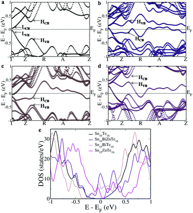
To study the effect of Bi–Zn co-doping on SnTe, we simulated Sn16Te16 and Sn14BiZnTe16 and compared their electronic structure and density of states (DOS) with those of Sn15BiTe16 and Sn15ZnTe16 (Fig. 1). A direct band gap of 0.08 eV appears at the Γ point in the Brillouin zone of Sn16Te16 due to the folding of the L point onto it, with the Fermi level passing exactly in between the band gap (Fig. 1a). Meanwhile, the heavy hole band appears at Z + δ in the Z → R direction due to the folding of the Σ point onto it. The energy difference (ΔEVB) between the light hole valence band at the Γ point and the heavy hole valence band at Z + δ in the Z → R direction is found to be 0.30 eV while that between the light hole conduction band at the Γ point and the heavy hole conduction band at Z + δ in the Z → R direction (ΔECB) is 0.24 eV.The electronic structure of Sn14BiZnTe16 reveals two resonance bands appearing almost as a mirror image with the Fermi level passing just beneath the valence band edge (Fig. 1b). Both these resonance levels cause asymmetric distortion in the DOS and appear in the form of two prominent peaks in the plot near the Fermi level (Fig. 1e). The heavy hole valence band of Sn14BiZnTe16 raises 0.27 eV above the valence band maximum (VBM) while the heavy hole conduction band drops 0.27 eV below the conduction band minimum (CBM).
To understand the contributions of each dopant atom, we analyzed the electronic structures of Sn15BiTe16 and Sn15ZnTe16. Sn15BiTe16 reveals a split off energy level from the conduction band touching the valence band at the Γ point 0.08 eV below the conduction band edge (Fig. 1c). The heavy hole conduction band drops 0.16 eV below the CBM and the second heavy hole conduction band at Z + δ in the Z → R direction remains 0.16 eV above the CBM, meanwhile ΔEVB remains at 0.30 eV. The DOS peak appears at the Fermi level, indicating the resonant nature of the Bi dopant.8
Interestingly, Sn15ZnTe16 also shows a split off energy level from the valence band touching the conduction band at the Γ point 0.08 eV above the valence band edge (Fig. 1d). The heavy hole valence band moves 0.15 eV above the VBM while the difference in the energy of the second heavy hole valence band at Z + δ in the Z → R direction from the light hole band at the Γ point remains at 0.30 eV. The heavy hole conduction band drops slightly lower with a ΔECB of 0.23 eV. The resonant level is also clearly visible in the DOS plot in the form of a hump near the Fermi level.9 The higher the contribution of resonant orbitals, the higher will be the rise in the energy of the band from the initial level.28 The almost flat nature of the band along the stretch of the A point in the R → Z direction indicates increased contribution from the resonant dopant at the A point leading to an increase in the energy level leading to improved Seebeck values.
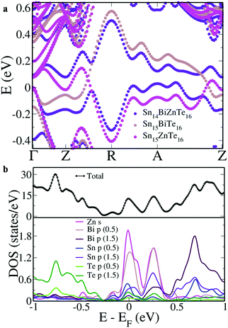
To get a better correlation between the co-doped and singly doped SnTe, we aligned the VBM of all the three structures (Fig. 2a). Unlike the singly doped case wherein the resonance states span across the valence band and conduction band area, in Sn14BiZnTe16, the two bands limit themselves to a single region. But, on careful observation, the mixing of the resonance levels is clear. From the Γ point to the mid way between Z → R, the resonance level in the valence band area is formed due to Bi orbitals while that in the conduction band area is due to Zn orbitals. There onwards, we see the contributions reversed due to the hybridization of the orbitals till Z–δ′ in the A → Z direction after which there is again a reversal.
To study the atomic contributions, when we project the DOS onto the atomic orbitals, we observe that the Bi ‘p’ orbitals hybridize with Zn ‘s’ orbitals along with a major contribution from Sn ‘p’ and a minor contribution from Te ‘p’ orbitals near the Fermi level (Fig. 2b). To get a clear correlation between the electronic structure and pDOS, we aligned them parallelly in Fig. S1 (ESI†). The DOS hump closer to the Fermi level has a dominant contribution of Zn orbitals while the one above the Fermi level has a dominant contribution from Bi orbitals. Such an unusual feature is absent in the case of the In dopant, where the resonance level is formed by the hybridization of an In ‘s’ orbital and a Te ‘p’ orbital without the involvement of Sn ‘p’ orbitals.8 This unique mixing of the orbitals in Sn14BiZnTe16 leads to the appearance of mirror image kind resonance levels on either side of the electronic structure. The appearance of the heavy hole valence band above the light hole valence band by about 0.27 eV in Sn14BiZnTe16 leading to high room temperature Seebeck values is a feature previously reported in Mg–In co-doped Sn1−xPbxTe with a ΔEVB value of −0.16 eV.29 Such a feature was absent in Mg doped Sn1−xPbxTe, In doped Sn1−xPbxTe and Mg–In co-doped SnTe, indicating that a multidopant approach was essential.20,29,30 We see that the co-doping of Bi and Zn in lead free SnTe is able to produce the same effect at an enhanced magnitude highlighting the uniqueness of the combination and possibility of elimination of the multidopant approach with harmful elements like Pb.
As the transport properties predicted by the Boltzmann transport equation showed promising results (see ESI† for details, Fig. S2), we synthesized SnTe and Bi–Zn co-doped SnTe along with Bi and Zn singly doped SnTe. The concentration of Bi and Zn in SnTe is maintained at x = 0.04 since it was revealed in earlier reports that beyond x = 0.04, the dopants precipitate out.8 The XRD patterns of SnTe, Sn0.96Bi0.04Te, Sn0.96Zn0.04Te and Sn0.92Bi0.04Zn0.04Te are indexed to the rock salt structure of the Fm3m space group (Fig. 3a). The diffraction pattern of Sn0.92Bi0.04Zn0.04Te exhibited additional peaks that could be indexed to Zn. This indicated the formation of secondary phases, which is further confirmed by TEM and EDS analysis (Fig. S3 and Table S1, ESI†). The sample shows the precipitates of Zn of 2–5 nm size in the TEM image.
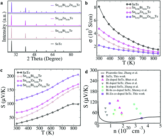 | ||
| Fig. 3 (a) XRD pattern (* indicates peaks due to the Zn precipitate); (b) electrical conductivity; (c) Seebeck coefficient of SnTe and doped samples as a function of temperature; (d) Seebeck coefficient values of SnTe and Bi–Zn co-doped SnTe at 300 K as a function of carrier concentration ‘n’ in comparison with the Pisarenko line and earlier reports.7–9,31 | ||
SnTe is known to be a poor thermoelectric material and the large number of Sn vacancies leading to a high carrier concentration ‘n’ is one of the reasons for it. The higher ‘n’ value (3.5 × 1020 cm−3) and higher mobility ‘μ’ (144.5 cm2 V−1 s−1) lead to a high electrical conductivity ‘σ’ of SnTe (8100 S cm−1). ‘n’ is seen to decrease with Bi/Zn doping, indicating the neutralization of Sn vacancies (Table S2, ESI†). The co-doping further decreases the ‘n’ (0.947 × 1020 cm−3) and ‘μ’ (141.7 cm2 V−1 s−1) values, leading to low ‘σ’ and high ‘S’ values. The ‘σ’ values of all the samples decrease with the temperature, indicating the degenerate semiconducting nature (Fig. 3b). The ‘S’ value of the doped samples is seen to be higher than that of pristine SnTe throughout the temperature range and that of the co-doped samples is higher than the singly doped samples (Fig. 3c). The positive values indicated the p-type nature. The introduction of resonance states and the dominance of the heavy hole band at room temperature lead to a valley degeneracy (Nv) value of 16 (12 from heavy hole and 4 from light hole).1 Since this is directly proportional to ‘S’, we obtain an ‘S’ value of 112 μV K−1 at 300 K and 205 μV K−1 at 840 K for Sn0.92Bi0.04Zn0.04Te. Usually, the effect of band convergence is dominant at high temperature and high dopant concentration but the current combination of co-dopants is able to introduce the effect at lower temperatures.1 This is evident in the comparison plot of room temperature ‘S’ values with respect to their carrier concentration ‘n’ with the reported literature values and Pisarenko line (Fig. 3d). The Pisarenko line was derived using a two valence band model with an energy difference of 0.35 eV between the light hole and heavy hole valence sub-bands. The light hole effective mass was taken as 0.168 me and heavy hole effective mass was 1.92 me.31 For comparison with previous reports, the Seebeck values of Zn, Bi, In and Bi–In co-doped SnTe have been marked with respect to their carrier concentrations.7–9,31 The Seebeck value of SnTe falls exactly in line with the Pisarenko value, indicating the effectiveness of the model employed. The resonant doped and co-doped samples show higher ‘S’ values than predicted by the Pisarenko line due to the modification of the electronic structure. The Bi–Zn co-doped sample has a higher ‘S’ value than previously reported Bi doped samples but it is slightly lower than that of previously reported Zn doped samples at 300 K.7,9 This indicates the prominence of the heavy hole dominance exhibited by Zn doped samples with a higher Zn concentration of 0.08 mol% compared to our co-doped sample with a Zn concentration of 0.04 mol%.9 Although the ‘S’ values of the co-doped sample are not as high as those of the Zn doped samples, the decrease in the thermal conductivity values due to the mass fluctuations created by Bi and Zn co-doping enhances the ZT throughout the temperature range in comparison to Zn doped SnTe as explained in the later sections.9
The increase in the power factor from ∼27 μW cm−1 K−2 at 300 K to ∼36 μW cm−1 K−2 at 840 K for Sn0.92Bi0.04Zn0.04Te is attributed to the increase in ‘S’ despite the decrease in ‘σ’ with the increase in the temperature (Fig. S4a, ESI†). Such a high power factor is promising in comparison to Mn–Cu–Ge multi-doped SnTe (∼19 μW cm−1 K−2 at 900 K) with a record ZT peak of ∼1.8.25 The comparison of Sn0.92Bi0.04Zn0.04Te with the state of the art SnTe based materials with a high power factor reveals that the material fares really well (Fig. S4b, ESI†). The total thermal conductivity is seen to decrease due to the decrease in the electronic as well as the lattice component of the thermal conductivity with temperature (Fig. 4a). The decrease in the carrier concentration leads to a decrease in the conductivity leading to lower electronic thermal conductivity values. The substitution of Bi/Zn for Sn introduces mass fluctuation and the atomic defects created enhance phonon scattering.1,8,9 In addition, the nano precipitates formed also effectively scatter the phonons, decreasing the lattice thermal conductivity to 0.68 W m−1 K−1 for Sn0.92Bi0.04Zn0.04Te (Fig. 4b).1,3,7,8 A comparison of the lattice thermal conductivity values of the present material with the state of the art SnTe based materials containing resonant dopants such as In, Bi and Zn reveals that the Sn0.92Bi0.04Zn0.04Te sample shows an appreciably lower value than both the Bi/Zn singly doped samples and also many of the co-doped samples.6–9,17,19,22,23 Though Cu–In and Sr–In co-doped SnTe have lower lattice thermal conductivities than Bi–Zn co-doped SnTe, their ZT values (∼1.55 and ∼1.31, respectively) are lower than that of the Bi–Zn co-doped SnTe.19,22 Thus, co-doping of Bi–Zn proves to be an effective strategy to improve the power factor and reduce the lattice thermal conductivity, and thereby the total thermal conductivity, leading to improved ZT values.
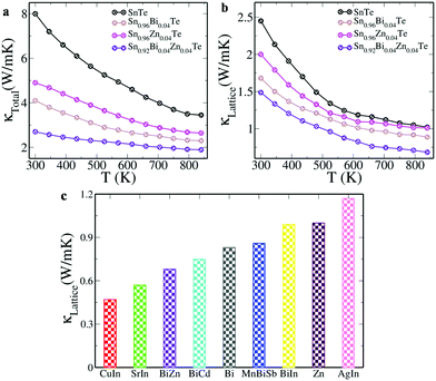 | ||
| Fig. 4 (a) Total thermal conductivity; (b) lattice thermal conductivity of SnTe and doped samples as a function of temperature; (c) comparison of lattice thermal conductivity of Sn0.92Bi0.04Zn0.04Te with the state of the art SnTe based materials.6–9,17,19,22,23 | ||
The interplay of the resonance levels in Sn0.92Bi0.04Zn0.04Te synergistically leads to a ZT of ∼0.3 at 300 K and a peak ZT of ∼1.6 at 840 K (Fig. 5). Such a high value of room temperature ZT sets a record for SnTe based materials. The material also attains a record high value of ZTaverage of ∼0.86 (with 300 K and 840 K as the cold and hot end) and ∼1.14 (with 500 K and 840 K as the cold and hot end), respectively. Here, the ZTaverage values are calculated by summing up the ZT throughout the said temperature range and dividing it by the number of instances. Even though a multi dopant approach of Mn–Cu–Ge doped SnTe reported a high peak ZT of ∼1.8 at 900 K, its ZTaverage was ∼0.76 (with 300 K and 900 K as the cold and hot end).24 Single crystalline SnSe, which by far holds a record high ZT (∼2.6 along the b axis) among chalcogenide materials, has a ZTaverage of ∼0.85 (with 300 K and 923 K as a cold and hot end), comparable with that of Sn0.92Bi0.04Zn0.04Te.32
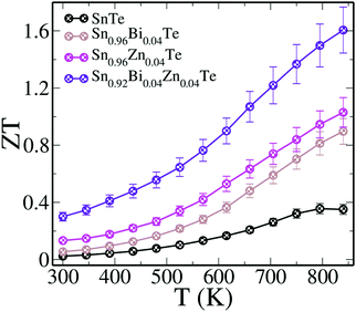 | ||
| Fig. 5 ZT of SnTe and doped samples as a function of temperature. The ZT measurement uncertainty is about 10% (error bar). | ||
Commercial application of thermoelectric materials requires them to possess a high ZTaverage not just a high peak ZT. The comparison of ZT (@300 K and @840 K) and ZTaverage with the reported high performing SnTe based materials clearly reveals the outperformance of the presently reported material (Fig. 6). Hence, Sn0.92Bi0.04Zn0.04Te shows great promise for future energy applications.
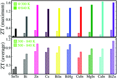 | ||
| Fig. 6 Comparison of ZT at 300 K and 840 K (upper panel); ZTaverage of SnTe and Sn0.92Bi0.04Zn0.04Te (lower panel) with the reported high performing SnTe based materials.7–9,11,14,18–20 | ||
4. Conclusions
In the present work, we modify the electronic structure of SnTe by introducing two resonant dopants, viz. bismuth and zinc. The interplay of the resonance states makes the heavy hole band dominant at room temperature. The nanoprecipitates formed and the atomic point defects introduced by dopant atoms decrease the lattice thermal conductivity to an appreciably low value of 0.68 W m−1 K−1 at 840 K. All these effects synergistically lead to a peak ZT of ∼1.6 at 840 K in the Sn0.92Bi0.04Zn0.04Te sample. It also exhibits a record high room temperature ZT of ∼0.3 at 300 K and record high ZTaverage values of ∼0.86 and ∼1.14 with 840 K as a hot end and 300 K and 500 K as a cold end, respectively. This strategy of co-doping two resonant dopants not only leads to an increase in the performance of the material throughout the temperature range but also motivates the researchers to look for such unusual combinations of dopants to constructively tune the electronic structure of materials.Conflicts of interest
The authors declare no competing financial interest.Acknowledgements
The authors gratefully acknowledge the financial support received from SERB and CSIR, Govt. of India in the form of R&D project grants and DST for INSPIRE Faculty award.References
- G. Tan, L. D. Zhao and M. G. Kanatzidis, Rationally Designing High-Performance Bulk Thermoelectric Materials, Chem. Rev., 2016, 116, 12123–12149 CrossRef CAS PubMed
.
- P. Ren, Y. Liu, J. He, T. Lv, J. Gao and G. Xu, Recent Advances in Inorganic Material Thermoelectrics, Inorg. Chem. Front., 2018, 5, 2380–2398 RSC
.
- R. Moshwan, L. Yang, J. Zou and Z. G. Chen, Eco-friendly SnTe Thermoelectric Materials: Progress and Future Challenges, Adv. Funct. Mater., 2017, 27, 1703278 CrossRef
.
- S. Li, X. Li, Z. Ren and Q. Zhang, Recent Progress Towards High Performance of Tin Chalcogenide Thermoelectric Materials, J. Mater. Chem. A, 2018, 6, 2432–2448 RSC
.
- S. X. Lin, X. Tan, H. Shao, J. Xu, Q. Wu, G. Q. Liu, W. H. Zhang and J. Jiang, Ultralow Lattice Thermal Conductivity in SnTe by Manipulating the Electron-Phonon Coupling, J. Phys. Chem. C, 2019, 123, 15996–16002 CrossRef CAS
.
- S. K. Kihoi, H. Kim, H. Jeong, H. Kim, J. Ryu, S. Yi and H. S. Lee, Thermoelectric Properties of Mn, Bi and Sb Co-doped SnTe With a Low Lattice Thermal Conductivity, J. Alloys Compd., 2019, 806, 361–369 CrossRef CAS
.
- Z. Zhou, J. Yang, Q. Jiang, Y. Luo, D. Zhang, Y. Ren, X. He and J. Xin, Multiple Effects of Bi Doping in Enhancing The Thermoelectric Properties of SnTe, J. Mater. Chem. A, 2016, 4, 13171–13175 RSC
.
- S. U. Shenoy and D. K. Bhat, Electronic Structure Engineering of Tin Telluride through Co-doping of Bismuth and Indium for High Performance Thermoelectrics: A Synergistic Effect Leading to Record High Room Temperature ZT in Tin Telluride, J. Mater. Chem. C, 2019, 7, 4817–4821 RSC
.
- D. K. Bhat and U. S. Shenoy, Zn: A Versatile Dopant for SnTe Thermoelectrics, Mater. Today Phys., 2019 DOI:10.1016/j.mtphys.2019.100158
.
- L. Zhao, J. Wang, J. Li, J. Liu, C. Wang, J. Wang and X. Wang, High Thermoelectric Performance of Ag Doped SnTe Polycrystalline Bulks via the Synergistic Manipulation of Electrical and Thermal Transport, Phys. Chem. Chem. Phys., 2019, 21, 17978–17984 RSC
.
- R. A. R. A. Orabi, N. A. Mecholsky, J. Hwang, W. Kim, J. S. Rhyee, D. Wee and M. Fornari, Band Degeneracy, Low Thermal Conductivity, and High Thermoelectric Figure of Merit in SnTe–CaTe Alloys, Chem. Mater., 2016, 28, 376–384 CrossRef
.
- R. Moshwan, X. Shi, W. Liu, L. Yang, Y. Wang, M. Hong, G. J. Auchterlonie, J. Zou and Z. G. Chen, High Thermoelectric Performance in Sintered Octahedron-shaped Sn(CdIn)xTe1+2x Microcrystals, ACS Appl. Mater. Interfaces, 2018, 10, 38944–38952 CrossRef CAS PubMed
.
- F. Guo, B. Cui, M. Guo, J. Wang, J. Cao, W. Cai and J. Sui, Enhanced Thermoelectric Performance of SnTe Alloy with Ce and Li co-doping, Mater. Today Phys., 2019 DOI:10.1016/j.mtphys.2019.100156
.
- G. Tan, F. Shi, J. W. Doak, H. Sun, L. D. Zhao, P. Wang, C. Uher, C. Wolverton, V. P. Dravid and M. G. Kanatzidis, Extraordinary Role of Hg in Enhancing the Thermoelectric Performance of p-type SnTe, Energy Environ. Sci., 2015, 8, 267–277 RSC
.
- A. Banik, U. S. Shenoy, S. Anand, U. V. Waghmare and K. Biswas, Mg Alloying in SnTe Facilitates Valence Band Convergence and Optimizes Thermoelectric Properties, Chem. Mater., 2015, 27, 581–587 CrossRef CAS
.
- F. Guo, B. Cui, Y. Liu, X. Meng, J. Cao, Y. Zhang, R. He, W. Liu, H. Wu, S. J. Pennycook, W. Cai and J. Sui, Thermoelectric SnTe with Band Convergence, Dense Dislocations, and Interstitials Through Sn Self-Compensation and Mn Alloying, Small, 2018, 14, 1802615 CrossRef PubMed
.
- A. Banik, U. S. Shenoy, S. Saha, U. V. Waghmare and K. Biswas, High Power Factor and Enhanced Thermoelectric Performance of SnTe-AgInTe2: Synergistic Effect of Resonance Level and Valence Band Convergence, J. Am. Chem. Soc., 2016, 138, 13068–13075 CrossRef CAS PubMed
.
- D. K. Bhat and S. U. Shenoy, Enhanced Thermoelectric Performance of Bulk Tin Telluride: Synergistic Effect of Calcium and Indium Co-doping, Mater. Today Phys., 2018, 4, 12–18 CrossRef
.
- F. Guo, B. Cui, H. Geng, Y. Zhang, H. Wu, Q. Zhang, B. Yu, S. J. Pennycook, W. Cai and J. Sui, Simultaneous Boost of Power Factor and Figure of Merit in In-Cu Co-doped SnTe, Small, 2019, 1902493 CrossRef PubMed
.
- D. K. Bhat and S. U. Shenoy, High Thermoelectric Performance of Co-doped Tin Telluride Due To Synergistic Effect of Magnesium and Indium, J. Phys. Chem. C, 2017, 121, 7123–7130 CrossRef CAS
.
- Z. Ma, J. Lei, D. Zhang, C. Wang, J. Wang, Z. Cheng and Y. Wang, Enhancement of Thermoelectric Properties in Pd-In Co-doped SnTe and Its Phase Transition Behavior, ACS Appl. Mater. Interfaces, 2019, 11, 33792–33802 CrossRef CAS PubMed
.
- R. Moshwan, W. D. Liu, X. L. Shi, Y. P. Wang, J. Zou and Z. G. Chen, Realizing High Thermoelectric Properties of SnTe via Synergistic Band Engineering and Structure Engineering, Nano Energy, 2019, 65, 104056 CrossRef
.
- Z. Chen, X. Guo, J. Tang, F. Xiong, W. Li, Y. Chen and R. Ang, Extraordinary Role of Bi for Improving Thermoelectrics in Low-Solubility SnTe-CdTe Alloys, ACS Appl. Mater. Interfaces, 2019, 11, 26093–26099 CrossRef CAS PubMed
.
- J. Tang, B. Gao, S. Lin, J. Li, Z. Chen, F. Xiong, W. Li, Y. Chen and Y. Pei, Manipulation of Band Structure and Interstitial Defects for Improving Thermoelectric SnTe, Adv. Funct. Mater., 2018, 28, 1803586 CrossRef
.
- P. Giannozzi, S. Baroni, N. Bonini, M. Calandra, R. Car, C. Cavazzoni, D. Ceresoli, G. L. Chiarotti, M. Cococcioni and I. Dabo,
et al., Quantum Espresso: a Modular and Open-Source Software Project for Quantum Simulations of Materials, J. Phys.: Condens. Matter, 2009, 21, 395502 CrossRef PubMed
.
- J. P. Perdew, K. Burke and M. Ernzerhof, Generalized Gradient Approximation Made Simple, Phys. Rev. Lett., 1996, 77, 3865–3868 CrossRef CAS PubMed
.
- G. K. H. Madsen, D. J. Singh and A. BoltzTrap., Code for Calculating Band Structure Dependent Quantities, Comput. Phys. Commun., 2006, 175, 67–71 CrossRef CAS
.
- X. J. Tan, G. Q. Liu, J. T. Xu, H. Z. Shao, J. Jiang and H. C. Jiang, Element-selective resonant state in M-doped SnTe (M = Ga, In, and Tl), Phys. Chem. Chem. Phys., 2016, 18, 20635–20639 RSC
.
- S. Roychowdhury, U. S. Shenoy, U. V. Waghmare and K. Biswas, An Enhanced Seebeck Coefficient and High Thermoelectric Performance in p-type In and Mg Co-doped Sn1−xPbxTe via The Co-adjuvant Effect of The Resonance Level and Heavy Hole Valence Band, J. Mater. Chem. C, 2017, 5, 5737–5748 RSC
.
- S. Shenoy and D. K. Bhat, Enhanced Bulk Thermoelectric Performance of Pb0.6Sn0.4Te: Effect of Magnesium Doping, J. Phys. Chem. C, 2017, 121, 20696–20703 CrossRef CAS
.
- Q. Zhang, B. Liao, Y. Lan, K. Lucas, W. Liu, K. Esfarjani, C. Opeil, D. Broido, G. Chen and Z. Ren, High Thermoelectric Performance by Resonant Dopant Indium in Nanostructured SnTe, Proc. Natl. Acad. Sci. U. S. A., 2013, 110, 13261–13266 CrossRef CAS PubMed
.
- L. D. Zhao, S. H. Lo, Y. Zhang, H. Sun, G. Tan, C. Uher, C. Wolverton, V. P. Dravid and M. G. Kanatzidis, Ultralow Thermal Conductivity and High Thermoelectric Figure of Merit in SnSe Crystals, Nature, 2014, 508, 373 CrossRef CAS PubMed
.
Footnote |
| † Electronic supplementary information (ESI) available: Electronic structure and pDOS of Sn14BiZnTe16, variation of DOS, Seebeck, electrical and thermal conductivity as a function of chemical potential, TEM image, EDS results, carrier concentration and mobility of samples, variation of power factor with temperature, and comparison of power factors with state of the art materials. See DOI: 10.1039/c9tc06490g |
| This journal is © The Royal Society of Chemistry 2020 |

