 Open Access Article
 This Open Access Article is licensed under a
 Creative Commons Attribution 3.0 Unported Licence
Model systems in heterogeneous catalysis: towards the design and understanding of structure and electronic properties
Q.
Pan
a,
L.
Li
a,
S.
Shaikhutdinov
a,
Y.
Fujimori
a,
M.
Hollerer
b,
M.
Sterrer
b and
H.-J.
Freund
*a
aFritz-Haber-Institute of the Max-Planck Society, Department of Chemical Physics, Faradayweg 16, 14195 Berlin, Germany. E-mail: freund@fhi-berlin.mpg.de
bUniversity of Graz, Institute of Physics, NAWI Graz, Universitätsplatz 5, 8010 Graz, Austria
First published on 6th December 2017
Abstract
We discuss in this paper two case studies related to nano-particle catalyst systems. One concerns a model system for the Cr/SiO2 Phillips catalyst for ethylene polymerization and here we present XPS data to complement the previously published TPD, IRAS and reactivity studies to elucidate the electronic structure of the system in some detail. The second case study provides additional information on Au nano-particles supported on ultrathin MgO(100)/Ag(100) films where we had observed a specific activity of the particle’s rim at the metal–oxide interface with respect to CO2 activation and oxalate formation, obviously connected to electron transfer through the MgO film from the metal substrate underneath. Here we present XPS and Auger data, which allows detailed analysis of the observed chemical shifts. This analysis corroborates previous findings deduced via STM.
Introduction
Catalysts are complex materials! Take heterogeneous catalysis, which is the topic of the present paper, as an example: a reaction between gaseous components proceeds at the surface of a solid material usually containing several components. In order to identify the active part of the catalyst we need to be able to study a very small amount of starting material and products at the surface of the complex material, and we need to be simultaneously able to differentiate the surface of the material from its bulk. This requires the development of specific, surface sensitive techniques and, in order to isolate the action of the various material components, a systematic variation in the complexity of the studied material.1 This variation has to proceed from the most simple to the more complex, and not vice versa. Only by adding complexity will we be able to finally approach the final real system. In this sense, we set up model systems in catalysis, which may be characterized at the atomic level. In addition, we note that progress in the spirit of understanding phenomena at the atomic level will only be achieved through experiment and theory going hand-in-hand.2Since the complex structure of real, supported metal catalysts often hampers the attempt to connect macroscopic effects with the microscopic processes taking place on the surface, an increasing number of model studies have been conducted so far to tackle these questions. For studies of that kind, planar substrates, instead of the technically used porous materials, are needed in order to take full advantage of modern surface spectroscopic and microscopic techniques.3,4 Vapor deposition of metals5–7 or deposition of metal clusters from the gas phase8 under ultrahigh vacuum (UHV) conditions has been preferred in experiments aimed at more fundamental questions about the correlation between the structure and properties of small metal particles.
In these cases, well-ordered substrates are desirable, in order to know where the atoms are. The most straightforward choice in this context is a single crystal sample, of course. Studies of bulk oxides, however, may suffer from severe experimental problems. Their insulating character can restrict or even prevent electron and ion spectroscopic measurements, as well as low-energy electron diffraction (LEED) and scanning tunneling microscope (STM) measurements. It is only in cases where the oxide can be made sufficiently bulk conducting (e.g. TiO2), that this limitation may not apply.9,10 Other difficulties encountered are related to sample mounting and cleaning (adjustment of surface stoichiometry) or arise from the poor thermal conductivity associated with oxide materials. In this context, ultra-thin oxide films grown on a metallic substrate are excellent alternatives in order to circumvent all of these problems.6,7,11,12 It has been shown that even films with a thickness of just a few Angstroms may exhibit physical properties characteristic of the bulk material.13 The traditional method to prepare such films is the oxidation of the native metal13 or an alloy,14–17 although this often results in amorphous or polycrystalline overlayers (e.g. Al oxide on Al,18–21 or Si oxide on Si22,23) or films with a rather high defect density. This is due to the large mismatch which usually exists between the metal and the oxide lattice (e.g. NiO(100)/Ni(100)24). There are a few examples where well-ordered crystalline films can be obtained in this way (e.g. Cr2O3(111) on Cr(110)25–27 or Al2O3 on NiAl(110)14,15 and Ni3Al(111)16,17). Therefore, other routes have been proposed. Goodman et al., for example, extensively explored preparation techniques based on the evaporation of a metal (or non-metal) onto a host crystal, mostly a refractory metal, in an ambient oxygen atmosphere.11,12,28 This approach allows one to vary the oxide film thickness, and explore whether the oxide film-metal support interface influences the properties of the supported particles. In fact, the oxide film metal interface may be used to control charge transfer from the interface to the supported metal particle.
In this discussion we elaborate on two systems, which we have worked on recently. The first is the design of a model system for the Phillips catalyst (Cr/SiO2) for ethylene polymerization, and the second one is the design of a system that allows us to study the action of the oxide-metal nanoparticle interface at the atomic level, i.e. Au nano-particles on MgO(100)/Ag(100).
(a) Model for the Phillips catalyst
The Phillips catalyst (Cr/SiO2) is used in the large-scale production of polyethylene and has attracted considerable attention in the catalytic community over the last sixty years.29–32 However, the atomic structure of the active site(s) and the reaction mechanism remain controversial, in particular due to the structural complexity and surface heterogeneity of the amorphous silica.33–39 However, recently developed thin silica films grown on metals as a well-defined silica support offers the opportunity to investigate mechanistic aspects of the reaction at the atomic scale.40–43 The so-called “bilayer” film grown on Ru(0001) consists of two silicate layers, each being formed by the corner sharing of SiO4 tetrahedra like in sheet silicates, and the film is weakly bonded to the metal surface.44,45Fig. 1(a) shows high-resolution microscopy images of the film surface, obtained in our own laboratories, that are superimposed with a network of N-membered silica rings. Being terminated by fully saturated siloxane bonds and hence essentially hydrophobic, the silica surface could, however, be hydroxylated with the help of low energy electron radiation.46 It was thought that surface hydroxyls would be acting as anchors for chromium species deposited from certain precursors, ultimately resulting in a well-defined planar model system, schematically shown in Fig. 1(b). These systems could, in principle, be characterized with atomic resolution using STM in combination with other spectroscopic techniques employed in surface science.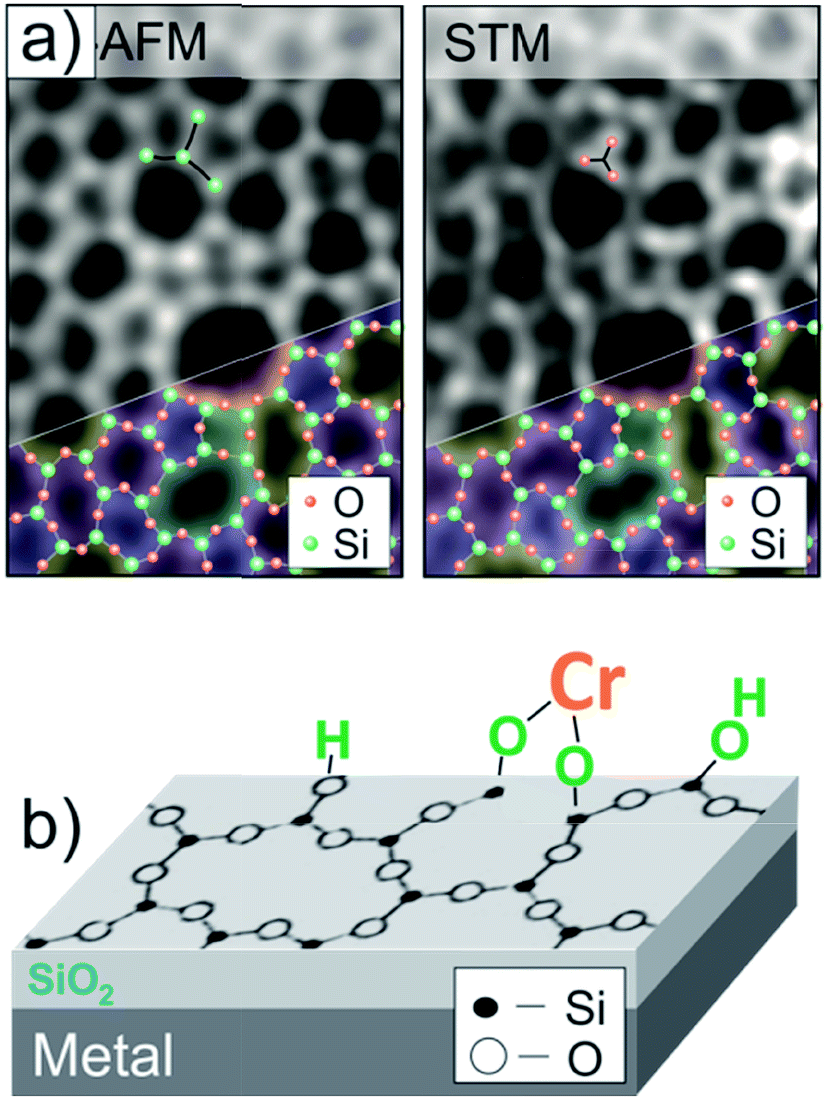 | ||
| Fig. 1 (a) Atomic force microscope (AFM) and STM images of the amorphous bilayer silica film grown on Ru(0001), that are superimposed with a silica network. (b) Schematic view of a planar model system for the Phillips catalyst, where Cr species are anchored onto an atomically flat hydroxylated silicate film (reprinted with permission from ref. 43. Copyright (2017) Elsevier). | ||
In a previous infrared reflection-absorption spectroscopy (IRAS) and temperature programmed desorption (TPD) study, we used Cr physical vapor deposition,43 which led to the reaction of Cr with silanol (Si–OH) species as evidenced by the disappearance of the corresponding IRA band. The adsorption of CO as a probe molecule showed a broad IRA signal at 2055 cm−1 and a weak band at 2160 cm−1, which were assigned to CO adsorbed on “naked” Cr sites and on Cr![[double bond, length as m-dash]](https://www.rsc.org/images/entities/char_e001.gif) O species, respectively. On the basis of TPD results, the amount of chromyl species is found to be relatively small. The system is fairly stable as no spectral changes were observed upon heating to 400 K under UHV. In ambient oxygen at elevated temperatures, Cr species become oxidized, thus forming more mono-chromyl species (and their aggregates) and probably di-oxo chromyl species which do not coordinate CO.
O species, respectively. On the basis of TPD results, the amount of chromyl species is found to be relatively small. The system is fairly stable as no spectral changes were observed upon heating to 400 K under UHV. In ambient oxygen at elevated temperatures, Cr species become oxidized, thus forming more mono-chromyl species (and their aggregates) and probably di-oxo chromyl species which do not coordinate CO.
Ethylene adsorption experiments on our model systems were conducted under UHV conditions at low temperature. The observed IRA bands at 2960 and 2874 cm−1, and 1462 and 1381 cm−1 are characteristic for stretching ν(C–H) and bending δ(C–H) vibrations, respectively, in R–CH3 groups. Accordingly, the bands at 2931, 2862 and 1462 cm−1 are assigned to C–H vibrations in R–CH2–R.47 Combined with IRAS results, the TPD spectra indicated the formation and desorption of butene even at 110 K, probably from butadiyl species.48 The desorption signals at ∼120 K were assigned to a mixture of ethylene and butane. This formation of C4 molecules at low temperatures would be consistent with the two-step initiation mechanism proposed by Scott and co-workers, in which n-butane is formed.33 It has recently been suggested that butene formation results from ethylene oligomerization.49,50
To shed more light on the structure of our model system, we carried out XPS measurements. The O 1s signal in the pristine films on Ru(0001) contains a main signal at 531.6 eV, assigned to oxygen atoms in the various Si–O–Si bonds in the film, and a shoulder at 529.4 eV, assigned to chemisorbed O atoms on Ru(0001) (Fig. 2(a)), in agreement with previous studies.40,51–53
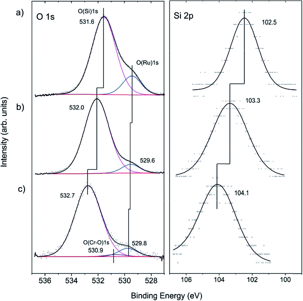 | ||
| Fig. 2 The O 1s and Si 2p regions of the XP spectra measured at normal electron emissions on: (a) a bilayer silicate film; (b) a hydroxylated silicate film; and (c) a hydroxylated silicate film after chromium deposition. The deconvolution envelope is shown in black. | ||
For hydroxylation of the silica surface, the film was pre-covered with a thin “ice” layer formed upon water adsorption at 100 K and subsequently irradiated with low energy (200 eV) electrons, as described in detail in ref. 46. The sample was then flashed to 300 K to ensure the desorption of molecular water. Electron bombardment greatly enhances the degree of hydroxylation without destroying the principal structure of the bilayer film as judged using IRAS and also STM, although atomic resolution was not achieved. Apparently, the hydroxylation occurs through the breaking of siloxane bonds in the silica network.43,54 In the course of XPS studies, we found certain beam damaging effects which are manifested in a lowering of the intensity of the silanol bands in IRAS after XPS measurements. However, the silanols can be fully recovered through the subsequent re-adsorption of water at 100 K and heating to 300 K. In order to minimize such effects, we used a lower number of scans for recording the Si 2p region, which, in contrast to the O 1s level, shows only one component. This explains the relatively low signal-to-noise ratio in the Si 2p spectra presented in Fig. 2.
Upon hydroxylation, the O(Ru) component (Fig. 2(b)) considerably attenuates and slightly shifts by about 0.2 eV, which is within the spectral resolution of our spectrometer (200 meV). However, the O(Si) and the Si 2p signals exhibit an obvious shift (0.4 eV and 0.8 eV, respectively) towards higher binding energies. In principle, the shifts could be explained by the loss of oxygen at the Ru-silica interface and respective changes in the work function of the substrate underneath the silica.51–53 Since the shift in the O(Si) core level is substantially different from the Si 2p one (0.4 vs. 0.8 eV), it is more plausible, however, that the observed shifts are, to a large extent, due to chemical changes in the silica framework caused by the formation of silanol bonds.43,46
Cr deposition onto hydroxylated films was carried out at low temperatures in order to prevent the migration of adsorbed metal atoms to the silica/support interface as previously observed for Pd.55 Also, to minimize the above-mentioned beam damaging effects, the XP spectra were recorded with only two scans both for the O 1s and Si 2p regions. Fig. 2(c) shows that the Si 2p level further shifts to higher energies by ∼0.8 eV. Concomitantly, a similar shift (∼0.7 eV) is found for the O(Si) component. In addition, a very weak signal at ∼530.9 eV is observed upon spectral deconvolution. The latter can, in principle, be attributed to the formation of Cr–O bonds, in agreement with IRAS results.43 The formation of Cr–O–Si bonds can also explain well the shift of the oxygen and silica signal towards higher binding energies.
To examine whether Cr migrates to the silica/Ru interface under our conditions, XP spectra were additionally measured at various electron emission angles (between 25 and 90° with respect to the surface plane). Due to the intentionally low amounts of chromium deposited and because of the strong overlap of the most intense Cr 2p signals and the Ru 3s core level, the binding energies of chromium could not precisely be determined. The deconvolution of the spectra (Fig. 3(a)) shows, however, that there are at least two Cr components (CrA and CrB). This would be consistent with the presence of “naked” Cr and CrO species observed through titration with CO. The peak area ratios between the Cr 2p and Si 2p signals are plotted in Fig. 3(b) as a function of the detection angle. The almost constant value of the peak area ratio suggests that most of the chromium species are located at the surface. Indeed, it is difficult to imagine that CO will penetrate through a silicate film at the low temperature used (85 K) and adsorb on the chromium species underneath, if they exist. Therefore, we may conclude that the shift of both O 1s signals and Si 2p signals upon Cr deposition reflects the bonding of Cr at the silica surface, which, in turn, modified the chemical environment of the atoms involved.
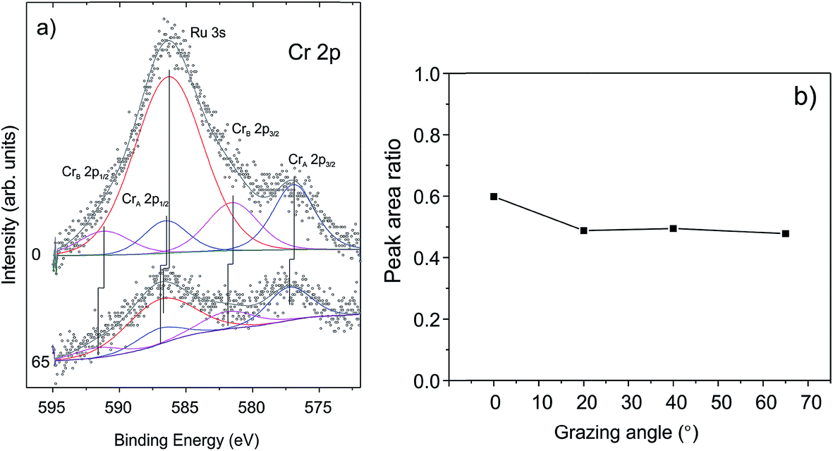 | ||
| Fig. 3 (a) The deconvoluted Cr 2p signals in XP spectra and (b) the peak area ratios of Cr 2p and Si 2p signals measured as a function of electron emissions. | ||
In summary, the XPS data presented in this paper nicely corroborate our previous results on the structure of the Phillips catalyst model system studied using IRAS and TPD. Further investigations, in particular with high resolution STM, are in progress to ultimately determine the atomic structure of the model catalysts.
(b) The oxide-nanoparticle interface
In order to design a model catalyst system that allows us to experimentally study the issues addressed above, a number of pre-requisites have to be fulfilled. Firstly, and foremost, the system has to represent oxide supported metal nano-particles as they are found in dispersed metal catalysts.56 A model is schematically shown in Fig. 4.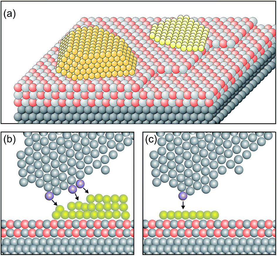 | ||
| Fig. 4 Schematic atomistic diagrams of two typical model catalyst systems (yellow: metal clusters, light grey and red: oxide film and gray: metal support). (a) Two nano-particles with different morphologies (left: 3-dimensional cluster, and right: 2-dimensional raft) supported on a thin oxide film, and (b) scanning tunneling microscope (STM) tip (grey atoms) approaching from above the rim of the nano-particle. The three atoms in blue at the front end and the side of the tip are responsible for the tunnel current. The black arrows indicate the tip surface interactions. Consequently, an atomically resolved topographic image of the 3D-cluster rim is difficult to obtain. (c) In contrast, the tunneling process to a well-defined 2D flat cluster is determined predominantly by the “last” atom of the tip (blue) which is closest to the flat surface. This situation allows us to obtain atomically resolved images of the whole cluster, and specifically of the cluster rim on a metal supported thin oxide film system. Reprinted with permission from ref. 56. | ||
Two nano-particles are placed on a thin, epitaxially grown oxide film on a metal support.4 The particles have different morphologies, i.e. one is a three-dimensional (3D) nano-particle and the other one assumes a two-dimensional (2D) raft morphology. Depending on the material combination, electrons may tunnel from the metal support underneath the insulating oxide film to the nano-particle supported on top of it. This process is governed by the energy it takes to remove an electron from the interface between the metal support and the thin oxide film (ionization potential of the interface), as well as by the energy released by placing one (or several) electron(s) onto the metal nano-particle on top of the oxide film (electron affinity of the metal nano-particle).57,58 The idea is that scanning tunneling microscopy and spectroscopy (STM, STS) should be well suited to detect this process. In particular, inelastic electron tunneling spectroscopy (IETS) would then – under specific conditions – provide evidence for the number of electrons involved in the transfer process. Furthermore, due to the ability to spatially resolve the local electron density we should be in a position to locate also where the electrons reside on the particle. Here the morphology of the nano-particle plays an important role. Consider the morphology of the nano-particle with respect to the size of the tunneling tip as schematically indicated in Fig. 4. It is obvious that a 3D particle may not be imaged in its entirety at atomic resolution. STM can, in principle, reveal only the exact arrangement of all atoms in a nano-particle if it is planar. For 3D nano-particles only the positions of the surface atoms can be mapped whereas the atomic arrangement on the lateral facets is in most cases difficult to obtain.
Only very recently Calaza et al.59 were able to record and image CO2 reactivity at the rim of two-dimensional Au rafts on MgO(100). As depicted in Fig. 5, in this study advantage was taken of two important factors: on the one hand we exploit the morphology (flat raft) of the pristine nano-particle (Fig. 5(a)), which allows us to access the perimeter in detail, and on the other hand we make use of the pronounced electron transfer towards the Au atoms residing at the perimeter, which may be used to induce chemical reactions.60–63 In the present case CO2 has been used as a reactant. Fig. 5(b) shows the Au-nano-particle decorated with CO2 at its perimeter, while the differential conductance spectroscopic image shown in Fig. 5(c) clearly reveals the increased electron density at the nano-particle rim (ref. 58). CO2 is a thermodynamically very stable molecule if no electrons are present. In the presence of electrons CO2 is activated through electron transfer. The energy cost to transfer an electron to CO2 is about 0.6 eV, but if one deals with a CO2 aggregate of at least two molecules the electron transfer becomes energetically favorable. For a dimer, in particular, the gain is 0.9 eV as determined through molecular beam experiments in the gas phase.64–66
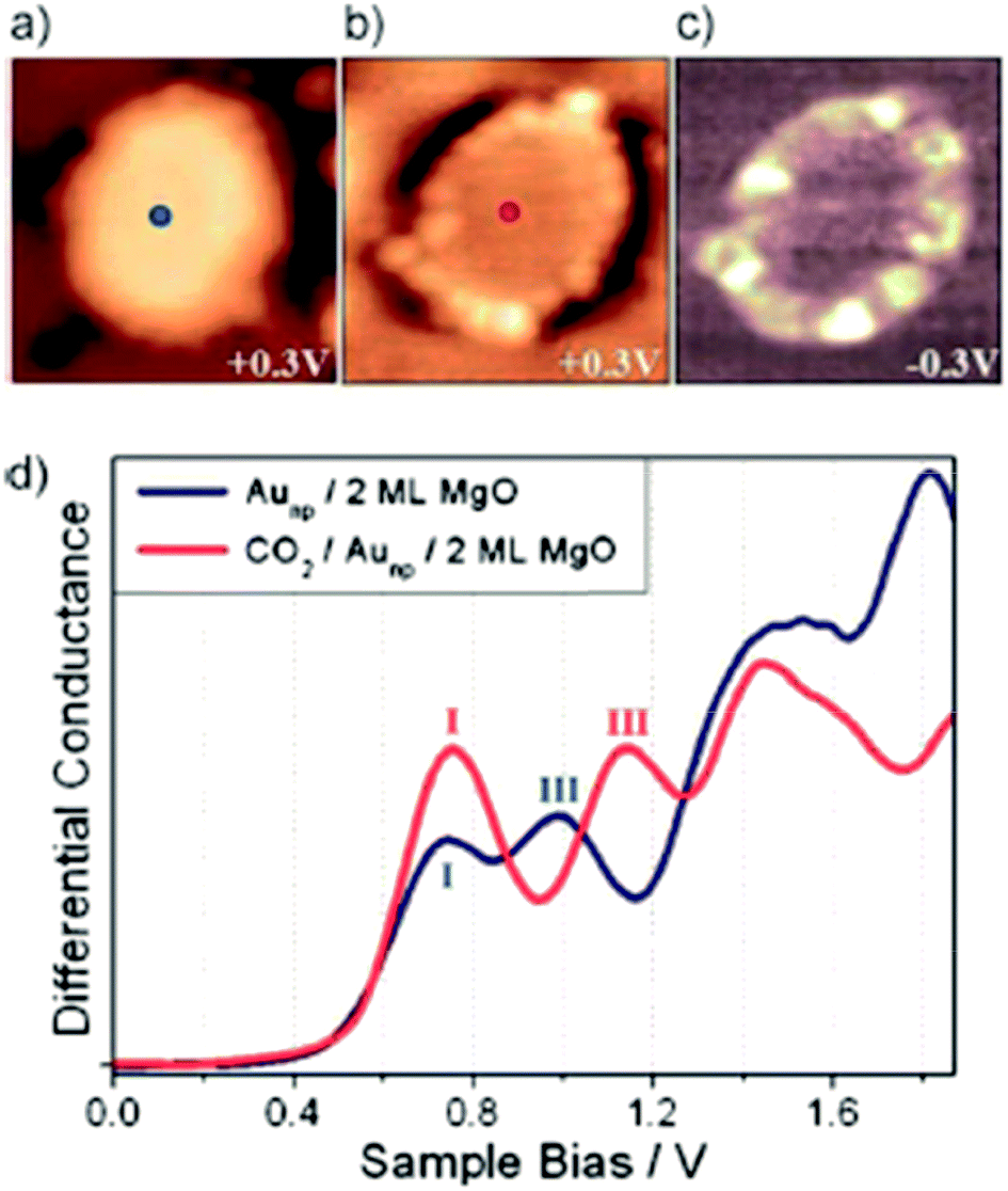 | ||
| Fig. 5 STM topographic images of a pristine planar Au cluster (a) before and (b) after exposure to CO2, (scan size 8.0 × 8.0 nm2, 50 pA). The Au clusters were prepared by evaporating Au on MgO mono- or bilayer films at 300 K. Subsequently the sample was exposed to 10–15 L of CO2 in a temperature range from 220 to 250 K. Molecules at the cluster perimeter in (b) become visible only when scanning at bias voltages between −0.5 and + 0.5 V. (c) Corresponding dI/dV map, displaying the high localization of electron density at the negatively charged cluster rim. (d) dI/dV spectra taken at the center of the clusters shown in (a) (blue) and (b) (red). The positions of the first (I) and third (III) quantum well state in both spectra are indicated. Note the energy shift towards higher energy of the internal energy scale of the cluster, which is compatible with a CO2 induced decrease of the electron potential well formed by the Au island from ref. 59. | ||
Since the reaction of a CO2 dimer to an oxalate (C2O42−) molecule has been observed on metal surfaces, which had been electron enriched through alkali adsorption,67 it is not surprising that the electron-rich supported Au nano-particles induce the formation of oxalate molecules at their perimeter where the extra electrons are localized. According to the STM studies the reaction is confined to the rim of the particles and the nature of the created species is confirmed through ensemble averaging infrared reflection absorption spectroscopy (IRAS), including isotopic labeling studies. When one investigates the distribution of oxalate molecules along the perimeter one finds inhomogeneities, that may be connected to the above mentioned inhomogeneous distribution of extra electrons along the perimeter. To look deeper into this problem we will perform IETS measurements, which will allow us to investigate the exact nature of the individual molecular species and their formation. Here we present XPS and Auger data to evaluate the charge on the particles and point out the importance of separating initial and final state effects. To address this issue empirically, Wagner established the Auger parameter (α),68 which consists of the difference between the kinetic energies (KEs) of XPS and Auger peaks from the same atom in a given material.69
The change noted in this value (Δα) when comparing the same spectra for a given atom in different environments has been shown to relate to changes exclusively in the final state of core-level photoemission processes via the following equation:
| Δα = Δ(BEXPS + KEAuger) = 2ΔR, | (1) |
A central assumption of this general approach is that ΔBE (−Δεn − ΔRn) will be equal for all electrons, regardless of orbital n. This, however, is empirically false,70 especially when comparing changes in valence and deeper core levels,71 which many continue to do by incorporating easily accessed core-valence-valence Auger measurements into their α experiments. To circumvent this problem associated with the original definition put forth by Wagner, a modified Auger parameter (β) was created72 in which the following (more specific) relationship was proposed:
| Δβ = Δ[2EB(i) − EB(j) + EKin(jii)] = 2ΔRi. | (2) |
In this case β represents a combination of three experimentally measured values that are chosen in a way that no longer requires the assumptions of equality for all orbital energy differences, Δε, and relaxation energy differences, ΔR.73 If, for practical reasons, EB(j) is not accessible in an experiment, a modified version of eqn (2) can be used:
| Δβ = Δ[EB(i) + EKin(jii)] = 2ΔRi. | (3) |
Since ΔRi = 1/2Δβ and ΔEB = −Δεi − ΔRi, the initial-state orbital energy shift Δεi can straightforwardly be calculated. The initial- and final-state contributions to the core-level XPS BE shift are then obtained by ΔEB,initial = −Δεi and ΔEB,final = −ΔRi, since, by convention, Δε and ΔR refer to orbital energies and BE(i) = −ε(i). For the present discussion of Au nanoparticles on MgO thin film substrates a negative ΔEB,final, when referenced to atoms in a bulk-like environment, is then indicative of the presence of negatively charged species, and vice versa.
The XPS (Au4f) and Auger spectra (AuM5N67N67) of a clean Au(111) single crystal are shown in Fig. 6 and serve as bulk reference for Δβ determination in the present study. Spectral fitting gives a BE of 84.0 eV for the Au 4f7/2 component, as expected. The M5N67N67 Auger transition consists of three microstates, of which the most intense (1I6, two holes in the 4f, l = +3 orbital) at 2015.5 eV KE was used for analysis.
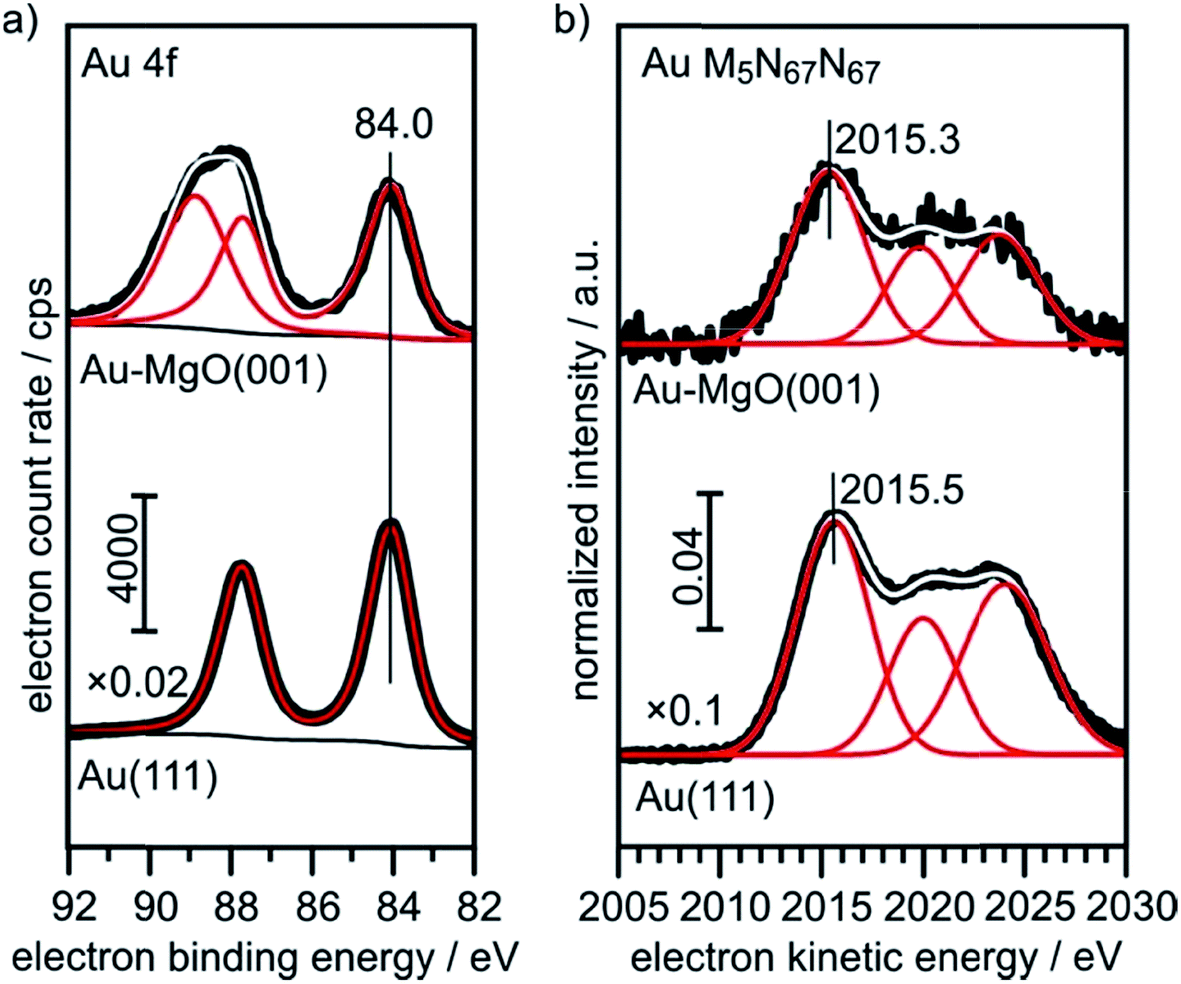 | ||
| Fig. 6 XPS and X-ray excited Auger reference spectra of Au(111) and 0.4 ML Au on 30 ML MgO(001)/Ag(001). | ||
For comparison, we show in Fig. 6 the spectra obtained from large, 3-dimensional Au nano-particles supported on a thick (30 ML) MgO(001) film grown on Ag(001), which has been prepared through the deposition of 0.4 MLE Au at room temperature and subsequent annealing at 573 K. The second component in the Au4f spectra of Au on MgO(001) is due to Mg 2s ionization. There is basically no observable shift between the pure metal substrate and the nano-particulate system in the XPS and Auger spectra, confirming that most of the atoms in the large Au nano-particles are in a bulk-like environment. These spectra need to be compared with those from 0.02 monolayers of Au on a three layer MgO film and on a thirty layer MgO film, taken directly after deposition at 100 K and after annealing at 300 K and 573 K, respectively (Fig. 7). Due to the low Au concentration the spectra are considerably noisier, but they may be clearly fitted by the equivalent components used to fit the spectra in Fig. 6. Note that the spectra obtained directly after deposition at 100 K can only be fitted through the inclusion of two Au species, with one species featuring a considerably higher binding and smaller electron kinetic energy. We will see below that this is compatible with positively charged Au particles even for the ultrathin film.
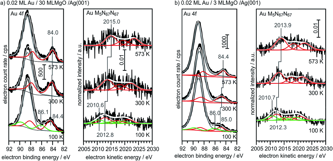 | ||
| Fig. 7 XPS and X-ray excited Auger spectra of 0.02 ML Au/30 ML MgO (a) and 0.02 ML Au/3 ML MgO (b) for different annealing temperatures (bottom: 100 K; middle: 300 K; top: 573 K). | ||
Via the combination of XPS binding energy shifts and kinetic energy shifts in Auger spectra we are in a position to calculate the modified Auger parameter, which allows a separation of initial state effects, directly connecting to the charge of the particle, and the final state effects due to the screening of the final hole-state. Table 1 summarizes the XPS and Auger data as well as the initial and final state contributions according to the modified Auger parameter (β). Fig. 8 shows a graphical representation of the various shifts. At 100 K, before the system has been equilibrated, there are positively charged Au species, possibly caused by the deposition process or the nucleation of gold on defect sites, present on both the ultrathin and the thick MgO(001) films. Their presence is consistent with the results of previous XPS and IRAS studies of Au deposited on MgO(001)/Ag(001) thin films.74 After heating to 300 K the system equilibrates, the positively charged species have disappeared, and the shifts change considerably. In the following we only discuss the situation after equilibration. In the case of the thick MgO film the initial state shifts of the main component are small and negative, indicating only minor charge transfer across the Au/MgO interface, and the BE shifts observed in XPS are dominated by final-state contributions. The decrease of ΔBEfinal with increasing annealing temperature, which reflects the enhanced possibility of the Au 6s electrons to screen the hole, is consistent with thermally induced particle coarsening.
| T K | Au 4f eV | Au M5N67N67 eV | ΔEB eV | ΔEkin eV | ΔEB,final eV | ΔEB,initial eV | |
|---|---|---|---|---|---|---|---|
| Au(111) | 300 | 84.0 | 2015.5 | ||||
| 0.4 ML Au/30 ML MgO | 573 | 84.0 | 2015.3 | 0 | −0.2 | 0.1 | −0.1 |
| 0.02 ML Au/3 ML MgO | 100 | 84.39 | 2012.8 | 0.39 | −2.70 | 1.155 | −0.765 |
| 86.15 | 2010.6 | 2.15 | −4.90 | 1.375 | 0.775 | ||
| 300 | 84.14 | 2013.69 | 0.14 | −1.81 | 0.835 | −0.695 | |
| 573 | 84.0 | 2015 | 0 | −0.50 | 0.25 | −0.25 | |
| 0.02 ML Au/30 ML MgO | 100 | 84.96 | 2012.32 | 0.96 | −3.18 | 1.11 | −0.15 |
| 86.04 | 2010.67 | 2.04 | −4.83 | 1.395 | 0.645 | ||
| 300 | 84.70 | 2013.1 | 0.7 | −2.40 | 0.85 | −0.15 | |
| 573 | 84.46 | 2013.9 | 0.46 | −1.60 | 0.57 | −0.11 |
 | ||
| Fig. 8 Graphical representation of the EB-shifts derived from Δβ measurements for 0.02 ML Au on 3 ML MgO(001)/Ag(001) (left) and 0.2 ML Au on 30 ML MgO(001)/Ag(001) (right) with reference to Au(111) from Table 1. | ||
The situation is different for the ultrathin MgO films: here the initial state shifts are considerably bigger and negative indicating negatively charged Au particles. In particular, we note that, while the final state shifts follow a similar trend for Au on the ultrathin and the thick MgO films, the ΔEB,initial contribution remains large after annealing at 300 K and gets considerably reduced only after heating to 573 K. The latter finding is consistent with a strong reduction of the number of negatively charged, interfacial Au atoms and indicates a change of the Au particle morphology. This is corroborated by inspection of the STM images of Au deposited on ultrathin (2 ML) MgO(001) films shown in Fig. 9 where the particle sizes and their distributions are represented for different Au deposition temperatures (Fig. 9(a) and (b)) and sample annealing temperatures (Fig. 9(c)–(f)). Some of these images have been published in a previous study,75 where we had indicated that in a temperature range around 450 K the particles change from a 2-dimensional to a 3-dimensional morphology. Here, we include results for a larger set of annealing temperatures and, in light of the discussion about CO2 activation noted at the beginning of this chapter, focus in particular on the evaluation of the images with respect to mean particle area and length of the particle perimeter (Fig. 9(g) and (h)).
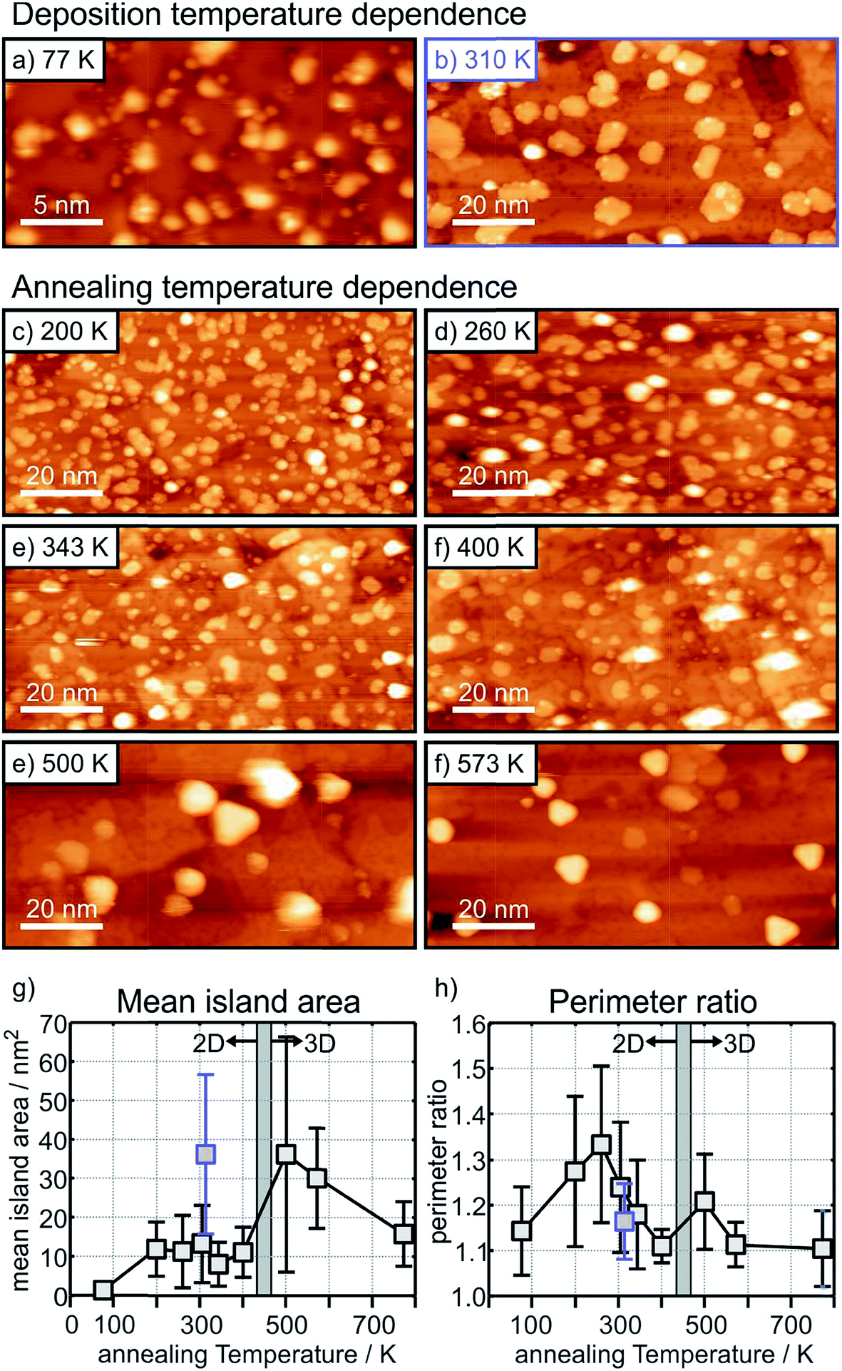 | ||
| Fig. 9 STM images taken at LN2 temperature of Au islands and nanoparticles on 2 monolayers MgO(001)/Ag(001) formed after deposition at 77 K (a), 25 nm × 13 nm, and 310 K (b), 100 nm × 50 nm, and after annealing the sample shown in (a) at a progressively higher temperature, (c–f), 100 nm × 50 nm. Tunneling conditions: Ubias = +(0.5–0.75) V, It = 30 pA. The mean Au island area and perimeter ratio (see text) are plotted as a function of the annealing temperature in (g) and (h). (Note: the large error bar of the data point at 500 K results from the poor image quality due to a bad STM tip). | ||
Fig. 9(a) and (b) (a: 25 nm × 13 nm, and b: 100 nm × 50 nm) have been taken directly after deposition at 77 K and 310 K, respectively. At 77 K very small islands and individual atoms are observed, and we know from previous studies that this leads to positively charged species.74 At deposition at room temperature larger flat islands are formed. Fig. 9(c) to (f) are images taken after heating to the given temperatures starting from the 77 K preparation.
It is clear from Fig. 9(g) that after an initial particle agglomeration between 100 K and 200 K the mean particle area remains rather constant between 200 K and 400 K, in the temperature range where 2-dimensional Au particles are stable. After crossing the 2D-to-3D transition, the mean particle area first increases, but decreases again at higher annealing temperatures due mainly to approaching a more favorable spherical particle shape. Note that 2-dimensional Au particles prepared through deposition at room temperature have a much larger mean particle area than those obtained through annealing the low-temperature deposits to a similar temperature (compare Fig. 9(b) and (e) and see the blue mark in Fig. 9(g)), which hints at different nucleation properties and diffusion barriers at the different deposition and annealing temperatures. Most important for the present discussion is the morphological change of the 2-dimensional particles at annealing temperatures between 200 K and 400 K. While the particles display rather arbitrary shapes below 300 K (Fig. 9(c) and (d)), they exhibit a more regular circular shape, and hence a reduced fraction of perimeter atoms, at higher temperature (Fig. 9(e) and (f)). To put this observation in a more quantitative term we plot in (Fig. 9(h)) the perimeter ratio, which is defined as the ratio of the observed perimeter length of an island in relation to the perimeter length of a circular island with the same area, as a function of temperature. It is clear that there is a maximum at 260 K. Since between 200 K and 400 K the island size remains constant one may conclude that the activity might be highest for a sample prepared by annealing to 260 K because the number of perimeter atoms is largest in this case. This conclusion is based on the discussion concerning CO2 activation discussed at the beginning of this chapter. This is a prediction that needs to be verified through future experiments.
Summarizing this part we notice that the detailed analysis of the XPS and Auger data corroborates the conclusions based on the analysis of the STM data in previous work, that the Au particles carry a negative charge, which is responsible for the observed reactivity of the rim of the particles towards the formation of oxalate species.
Conclusions
We have discussed two different case studies of oxide supported metal catalysts using a model approach. Here we presented mainly XPS data in order to complement results gained by a number of other techniques used in previous studies on the same systems. Since X-ray photoelectron spectroscopy is a generally applied technique, it is important to discuss those results in perspective to the available information. The case studies demonstrate that the simplest interpretation just using the observed shifts in binding energy would be misleading and that a more careful analysis based on a more sophisticated analysis allows us to retrieve information that corroborates results derived from a combination of complementary techniques.Acknowledgements
We thank the German Science Foundation (DFG) through the Cluster of Excellence UniCat and the Fonds der Chemischen Industrie for financial support.References
- H.-J. Freund, N. Nilius, T. Risse, S. Schauermann and T. Schmidt, ChemPhysChem, 2011, 12, 79–87 CrossRef PubMed.
- J. Sauer and H.-J. Freund, Catal. Lett., 2015, 145, 109–125 CrossRef.
- M. Bäumer and H.-J. Freund, Prog. Surf. Sci., 1999, 61, 127–198 CrossRef.
- H.-J. Freund, J. Am. Chem. Soc., 2016, 138, 8985–8996 CrossRef PubMed.
- C. T. Campbell, Surf. Sci. Rep., 1997, 27, 1–111 CrossRef.
- H. J. Freund, Angew. Chem., Int. Ed., 1997, 36, 452–475 CrossRef.
- M. Bäumer, J. Libuda and H.-J. Freund, in Chemisorption and Reactivity on Supported Clusters and Thin Films, ed. R. M. Lambert and G. Pacchioni, Kluwer Academic Publishers Dordrecht, 1997, vol. 331, pp. 61–104 Search PubMed.
- U. Heiz, F. Vanolli, L. Trento and W. D. Schneider, Rev. Sci. Instrum., 1997, 68, 1986 CrossRef.
- U. Diebold, J.-M. Pan and T. E. Madey, Surf. Sci., 1995, 331–333, 845 CrossRef.
- R. Persaud and T. E. Madey, in The Chemical Physics of Solid Surfaces, ed. D. A. King and D. P. Woodruff, Elsevier, 1997, vol. 8, pp. 407–447 Search PubMed.
- D. W. Goodman, Surf. Rev. Lett., 1995, 2, 9–24 CrossRef.
- D. W. Goodman, Surf. Sci., 1994, 299–300, 837–848 CrossRef.
- H.-J. Freund, Phys. Status Solidi B, 1995, 192, 407–440 CrossRef.
- R. M. Jaeger, H. Kuhlenbeck, H. J. Freund, M. Wuttig, W. Hoffmann, R. Franchy and H. Ibach, Surf. Sci., 1991, 259, 235–252 CrossRef.
- J. Libuda, F. Winkelmann, M. Bäumer, H.-J. Freund, T. Bertrams, H. Neddermeyer and K. Müller, Surf. Sci., 1994, 318, 61–73 CrossRef.
- U. Bardi, A. Atrei and G. Rovida, Surf. Sci., 1992, 268, 87–97 CrossRef.
- C. Becker, J. Kandler, H. Raaf, R. Linke, T. Pelster, M. Dräger, M. Tanemura and K. Wandelt, J. Vac. Sci. Technol., A, 1998, 16, 1000–1005 Search PubMed.
- J. G. Chen, J. E. Crowell and J. T. Yates Jr, Surf. Sci., 1987, 185, 373–393 CrossRef.
- D. N. Belton and S. J. Schmieg, Surf. Sci., 1988, 199, 518–536 CrossRef.
- J. G. Chen, M. L. Colaianni, W. H. Weinberg and J. T. Yates Jr, Surf. Sci., 1992, 279, 223–232 CrossRef.
- D. N. Belton and S. J. Schmieg, Surf. Sci., 1988, 202, 238–254 CrossRef.
- F. Rochet, S. Rigo, M. Froment, C. d’Anterroches, C. Maillot, H. Roulet and G. Dufour, Adv. Phys., 1986, 35, 237–274 CrossRef.
- The Physics of SiO2 and its Interfaces, in Proceedings of the International Topical Conference on the Physics of SiO2 and Its Interfaces Held at the IBM Thomas J. Waston Research Center, ed. S. T. Pantelides, Pergamon Press, Yorktown Heights, New York, March 22-24, 1978 Search PubMed.
- M. Bäumer, D. Cappus, H. Kuhlenbeck, H. J. Freund, G. Wilhelmi, A. Brodde and H. Neddermeye, Surf. Sci., 1991, 253, 116 CrossRef.
- H. Kuhlenbeck, C. Xu, B. Dillmann, M. Haßel, B. Adam, D. Ehrlich, S. Wohlrab, H.-J. Freund, U. A. Ditzinger, H. Neddermeyer, M. Neuber and M. Neumann, Berichte der Bunsengesellschaft für physikalische Chemie, 1992, 96, 15 CrossRef.
- F. Rohr, M. Bäumer, H. J. Freund, J. A. Mejias, V. Staemmler, S. Müller, L. Hammer and K. Heinz, Surf. Sci., 1997, 372, L291–L297 CrossRef.
- R. Rohr, M. Bäumer, H. J. Freund, J. A. Mejias, V. Staemmler, S. Müller, L. Hammer and K. Heinz, Surf. Sci., 1997, 389, 391 CrossRef.
- D. W. Goodman, J. Vac. Sci. Technol., A, 1996, 14, 1526 Search PubMed.
- J. P. Hogan, J. Polym. Sci., Part A: Polym. Chem., 1970, 8, 2637–2652 CrossRef.
- E. Groppo, C. Lamberti, S. Bordiga, G. Spoto and A. Zecchina, Chem. Rev., 2005, 105, 115–184 CrossRef PubMed.
- B. M. Weckhuysen, R. A. Schoonheydt, J. M. Jehng, I. E. Wachs, S. J. Cho, R. Ryoo, S. Kijlstra and E. Poels, J. Chem. Soc., Faraday Trans., 1995, 91, 3245–3253 RSC.
- M. P. McDaniel, in Adv. Catal., ed. C. G. Bruce and K. Helmut, Academic Press, 2010, vol. 53, pp. 123–606 Search PubMed.
- C. Brown, J. Krzystek, R. Achey, A. Lita, R. Fu, R. W. Meulenberg, M. Polinski, N. Peek, Y. Wang, L. J. van de Burgt, S. Profeta, A. E. Stiegman and S. L. Scott, ACS Catal., 2015, 5, 5574–5583 CrossRef.
- E. Groppo, C. Lamberti, S. Bordiga, G. Spoto and A. Zecchina, J. Catal., 2006, 240, 172–181 CrossRef.
- E. L. Lee and I. E. Wachs, J. Phys. Chem. C, 2007, 111, 14410–14425 Search PubMed.
- M. P. Conley, M. F. Delley, G. Siddiqi, G. Lapadula, S. Norsic, V. Monteil, O. V. Safonova and C. Copéret, Angew. Chem., Int. Ed., 2014, 53, 1872–1876 CrossRef PubMed.
- M. F. Delley, F. Núñez-Zarur, M. P. Conley, A. Comas-Vives, G. Siddiqi, S. Norsic, V. Monteil, O. V. Safonova and C. Copéret, Proc. Natl. Acad. Sci. U. S. A., 2014, 111, 11624–11629 CrossRef PubMed.
- P. C. Thüne, J. Loos, A. M. de Jong, P. J. Lemstra and J. W. Niemantsverdriet, Top. Catal., 2000, 13, 67–74 CrossRef.
- P. C. Thüne, J. Loos, X. Chen, E. M. E. van Kimmenade, B. Kong and J. W. Niemantsverdriet, Top. Catal., 2007, 46, 239–245 CrossRef.
- B. Yang, W. E. Kaden, X. Yu, J. A. Boscoboinik, Y. Martynova, L. Lichtenstein, M. Heyde, M. Sterrer, R. Wlodarczyk, M. Sierka, J. Sauer, S. Shaikhutdinov and H.-J. Freund, Phys. Chem. Chem. Phys., 2012, 14, 11344–11351 RSC.
- S. Shaikhutdinov and H.-J. Freund, J. Phys.: Condens. Matter, 2015, 27, 443001 CrossRef PubMed.
- C. Büchner, L. Lichtenstein, X. Yu, J. A. Boscoboinik, B. Yang, W. E. Kaden, M. Heyde, S. K. Shaikhutdinov, R. Włodarczyk, M. Sierka, J. Sauer and H.-J. Freund, Chem.–Eur. J., 2014, 20, 9176–9183 CrossRef PubMed.
- Q. Pan, et al. , J. Catal., 2018, 357, 12–19 CrossRef.
- L. Lichtenstein, C. Büchner, B. Yang, S. Shaikhutdinov, M. Heyde, M. Sierka, R. Włodarczyk, J. Sauer and H.-J. Freund, Angew. Chem., Int. Ed., 2012, 51, 404–407 CrossRef PubMed.
- L. Lichtenstein, M. Heyde and H.-J. Freund, J. Phys. Chem. C, 2012, 116, 20426–20432 Search PubMed.
- X. Yu, E. Emmez, Q. Pan, B. Yang, S. Pomp, W. E. Kaden, M. Sterrer, S. Shaikhutdinov, H.-J. Freund, I. Goikoetxea, R. Wlodarczyk and J. Sauer, Phys. Chem. Chem. Phys., 2016, 18, 3755–3764 RSC.
- P. Larkin, in Infrared and Raman Spectroscopy, Elsevier, Oxford, 2011, pp. 55–62, DOI:10.1016/b978-0-12-386984-5.10004-7.
- I. Lee and F. Zaera, J. Phys. Chem. B, 2005, 109, 2745–2753 CrossRef PubMed.
- M. F. Delley, G. Lapadula, F. Núñez-Zarur, A. Comas-Vives, V. Kalendra, G. Jeschke, D. Baabe, M. D. Walter, A. J. Rossini, A. Lesage, L. Emsley, O. Maury and C. Copéret, J. Am. Chem. Soc., 2017, 139, 8855–8867 CrossRef PubMed.
- A. Fong, Y. Yuan, S. L. Ivry, S. L. Scott and B. Peters, ACS Catal., 2015, 5, 3360–3374 CrossRef.
- R. Włodarczyk, M. Sierka, J. Sauer, D. Löffler, J. J. Uhlrich, X. Yu, B. Yang, I. M. N. Groot, S. Shaikhutdinov and H.-J. Freund, Phys. Rev. B, 2012, 85, 085403 CrossRef.
- M. Wang, J.-Q. Zhong, J. Kestell, I. Waluyo, D. J. Stacchiola, J. A. Boscoboinik and D. Lu, Top. Catal., 2017, 60, 481–491 CrossRef.
- D. Löffler, J. J. Uhlrich, M. Baron, B. Yang, X. Yu, L. Lichtenstein, L. Heinke, C. Büchner, M. Heyde, S. Shaikhutdinov, H.-J. Freund, R. Włodarczyk, M. Sierka and J. Sauer, Phys. Rev. Lett., 2010, 105, 146104 CrossRef PubMed.
- W. E. Kaden, et al. , Top. Catal., 2017, 60, 471–480 CrossRef.
- C. Büchner, L. Lichtenstein, S. Stuckenholz, M. Heyde, F. Ringleb, M. Sterrer, W. E. Kaden, L. Giordano, G. Pacchioni and H.-J. Freund, J. Phys. Chem. C, 2014, 118, 20959–20969 Search PubMed.
- W.-D. Schneider, et al. , Chem.–Eur. J., 2018, 24, 2317–2327 CrossRef PubMed.
- D. Ricci, A. Bongiorno, G. Pacchioni and U. Landman, Phys. Rev. Lett., 2006, 97, 036106 CrossRef PubMed.
- M. Sterrer, T. Risse, M. Heyde, H.-P. Rust and H.-J. Freund, Phys. Rev. Lett., 2007, 98, 206103 CrossRef PubMed.
- F. Calaza, C. Stiehler, Y. Fujimori, M. Sterrer, S. Beeg, M. Ruiz-Oses, N. Nilius, M. Heyde, T. Parviainen, K. Honkala, H. Häkkinen and H.-J. Freund, Angew. Chem., Int. Ed., 2015, 54, 12484–12487 CrossRef PubMed.
- C. Stiehler, F. Calaza, W.-D. Schneider, N. Nilius and H.-J. Freund, Phys. Rev. Lett., 2015, 115, 036804 CrossRef PubMed.
- X. Lin, N. Nilius, M. Sterrer, P. Koskinen, H. Häkkinen and H.-J. Freund, Phys. Rev. B, 2010, 81, 153406 CrossRef.
- X. Lin, N. Nilius, H. J. Freund, M. Walter, P. Frondelius, K. Honkala and H. Häkkinen, Phys. Rev. Lett., 2009, 102, 206801 CrossRef PubMed.
- C. Stiehler, Y. Pan, W.-D. Schneider, P. Koskinen, H. Häkkinen, N. Nilius and H.-J. Freund, Phys. Rev. B, 2013, 88, 115415 CrossRef.
- A. Stamatovic, K. Stephan and T. D. Märk, Int. J. Mass Spectrom. Ion Processes, 1985, 63, 37–47 CrossRef.
- E. L. Quitevis and D. R. Herschbach, J. Phys. Chem., 1989, 93, 1136–1139 CrossRef.
- R. N. Compton, P. W. Reinhardt and C. D. Cooper, J. Chem. Phys., 1975, 63, 3821–3827 CrossRef.
- F. M. Hoffmann, M. D. Weisel and J. A. K. Paul, in Carbon Dioxide Chemistry, Woodhead Publishing, 1994, pp. 55–63, DOI:10.1016/b978-1-85573-799-0.50011-x.
- C. D. Wagner, Faraday Discuss. Chem. Soc., 1975, 60, 291–300 RSC.
- C. D. Wagner and A. Joshi, J. Electron Spectrosc. Relat. Phenom., 1988, 47, 283–313 CrossRef.
- R. N. Sodhi and R. G. Cavell, J. Electron Spectrosc. Relat. Phenom., 1983, 32, 283–312 CrossRef.
- P. S. Bagus, A. Wieckowski and H. Freund, Chem. Phys. Lett., 2006, 420, 42–46 CrossRef.
- G. Hohlneicher, H. Pulm and H.-J. Freund, J. Electron Spectrosc. Relat. Phenom., 1985, 37, 209–224 CrossRef.
- W. E. Kaden, C. Büchner, L. Lichtenstein, S. Stuckenholz, F. Ringleb, M. Heyde, M. Sterrer, H.-J. Freund, L. Giordano, G. Pacchioni, C. J. Nelin and P. S. Bagus, Phys. Rev. B, 2014, 89, 115436 CrossRef.
- M. A. Brown, F. Ringleb, Y. Fujimori, M. Sterrer, H.-J. Freund, G. Preda and G. Pacchioni, J. Phys. Chem. C, 2011, 115, 10114–10124 Search PubMed.
- C. P. O’Brien, K. H. Dostert, M. Hollerer, C. Stiehler, F. Calaza, S. Schauermann, S. Shaikhutdinov, M. Sterrer and H. J. Freund, Faraday Discuss., 2016, 188, 309–321 RSC.
| This journal is © The Royal Society of Chemistry 2018 |