DOI:
10.1039/D4MA00455H
(Paper)
Mater. Adv., 2024,
5, 6309-6318
Preparation of bismuth-doped CsPbBr3 perovskite single crystals for X-ray and gamma-ray sensing applications†
Received
2nd May 2024
, Accepted 25th June 2024
First published on 26th June 2024
Abstract
Perovskite materials are potential photo-absorbers, and their solution-processed perovskite layers are widely reported in photodetection devices. However, defects in perovskites pose a serious challenge to device performance. One possible way to overcome this set-back is growing a perovskite single crystal and deploying it in photon detection devices. Herein, we report the growth of pure and Bi-doped CsPbBr3 perovskite single-crystals and their high-energy photodetection characteristics. The Bi-doped CsPbBr3 perovskite single-crystals exhibited good photodetection characteristics in the visible, X-ray and gamma-ray regions. Under an illumination of 470 and 530 nm, the Bi-doped CsPbBr3 perovskite single-crystal photodetector displayed a linear response for the biasing voltage ranging from 2 V to 5 V. The device displayed a higher magnitude of photocurrent and exhibited a better ON/OFF ratio of ∼596 at λ = 470 nm and ∼24 at λ = 530 nm. The gamma ray detection properties of the Bi-doped CsPbBr3 perovskite single crystal were studied using two different radioactive sources with varying activity levels. A characterization study using a portable X-ray device revealed an excellent response to varying tube voltages and currents. The present study reveals the versatility of the Bi-doped CsPbBr3 perovskite single-crystals in photon detection under a wide range of illumination.
Introduction
Photodetectors are among the most commonly used sensor devices for acquiring information. Among the various radiation detectors, sensitive gamma-ray detectors are notable in various applications in medical imaging,1 nuclear energy,2 scientific research,3 and radiation protection.4,5 In general, two radiation detection techniques are used: direct and indirect. In the direct radiation detection technique, high-energy photons are mostly directly converted into electronic signals for which semiconductor crystals can be primary contenders.4,6,7 Semiconductor crystals are viable as gamma-ray spectral detectors as they have higher stopping power, higher mobility lifetime for efficient charge collection, large resistance to noise for better signal quality, lower trap density for decreased charge trapping, and low cost for a measurable structure.8,9 Gamma-ray spectroscopy can resolve the energy of incoming gamma rays and identify radio-active species and isotopes. Germanium has been widely used for gamma-ray spectroscopy for over 40 years.10,11 Recently, organic–inorganic lead halide perovskites have been demonstrated as a promising candidate for developing high performance radiation detectors because of their impressive optical and electronic properties,8,12 including long change-carrier diffusion lengths, tuneable bandgaps, low defect density,13 high mobility-lifetime (μτ) and unique defect tolerant nature.14 In recent decades, several semiconducting materials, such as CdTe,15,16 mercuric iodide (HgI2),2 and CdZnTe (CZT),17 have been studied for direct radiation detection applications.18 Unfortunately, none of them is an ideal candidate. Specifically, it is expensive to achieve high-quality spectral grade crystal CdZnTe, which is grown using the high-temperature processing Czochralski method. Lead halide perovskite-based materials are widely used in radiation detection and are considered important in this field.6,8 Several studies have tuned the optical and electronic characteristics of halide perovskites by doping them with certain hetero-valent cations. In this respect, cations In3+, Ag+, Sb3+ and Bi3+ are particularly interesting because their valence electronic shell is isoelectronic to lead, and the ns2 lone pair is essential for defect tolerance.19,20 In a highly symmetric chemical environment, certain ions combine to form narrow-band compounds that are essential for optical applications in halide perovskites. Bi3+ is of particular interest as a dopant due to its stability and ionic radius, which is similar to lead (1.03 and 1.19 A).21 One of the critical issues addressed by doping halide perovskites with bismuth is the possibility of shifting the absorption threshold toward longer wavelengths, which was assumed due to the optical bandgap tuning by the doping concentration level. It is found that the doping of bismuth into CsPbX3 ternary compounds, where X (Br or Cl), is known for its high density, high resistivity, and wide bandgap, makes them ideal materials for gamma-ray and X-ray detection at room temperature. The modified solution process was used to grow large single crystals of CsPbX3 compounds. CsPbBr3 has already been shown to be effective in detecting X-rays.22 However, even a tiny concentration of native defects and impurities can act as traps and recombination centres, negatively impacting the detector's performance. When photo-excited carriers are trapped at defects, it decreases the spectral resolution, and the surface recombination of carriers reduces the charge collection efficiency.23,24 Additionally, the value of μτ, an essential property of these materials, is degraded by defect concentrations as low as few ppm or even lower.24 Most measurement techniques lack the sensitivity due to detect defects at low levels.21 They cannot ignore native defects, such as vacancies and anti-site defects, which can reduce μτ values and detector efficiency.
In this paper, we successfully doped bismuth into a CsPbBr3 single crystal and found that it partially replaced Pb2+ with Bi3+ in the crystal system. Further, we studied their structural and photophysical properties using XRD, SEM, RAMAN and photoluminescence emission spectroscopy. We fabricated a planar-type photodetector device with an Au/Bi-doped CsPbBr3/Au structure and measured the dark current and photocurrent response at different wavelengths to evaluate the device performance. We also characterized the X-ray and gamma-ray sensing properties of the Bi-doped CsPbBr3 perovskite single-crystal photodetector and discussed the results in detail.
Experimental methods
Chemicals and reagents
Lead bromide (PbBr2 ≥98% Aladdin), cesium bromide (CsBr ≥99.9% Aladdin), bismuth iodide (BiI3 ≥99%, Aladdin) dimethyl sulfoxide (DMSO, ≥99.9%, Macklin), N,N-dimethylformamide (DMF, ≥99.5%, Aladdin) and cyclohexanol (CyOH) were purchased and used without further purification.
ITC growth of Bi-doped CsPbBr3 single crystals
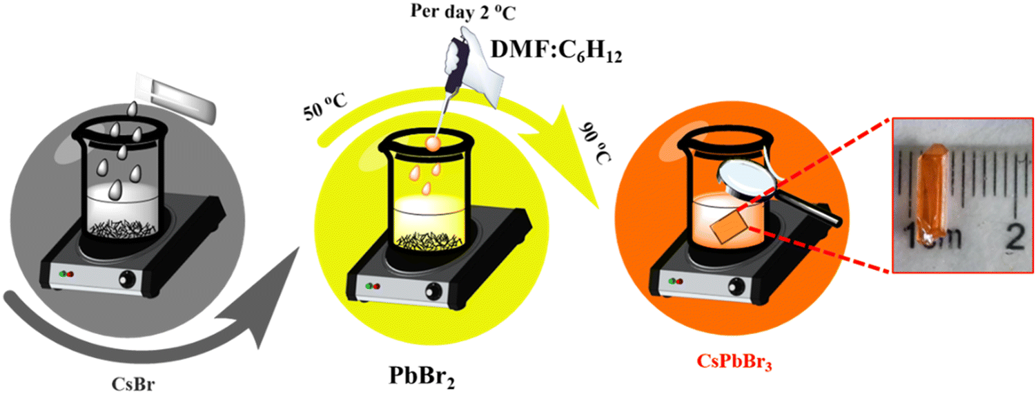
Single crystals of CsPbBr3 were grown by applying a modified inverse temperature recrystallization process.25,26 Initially, a mixture of dimethylsulfoxide (DMSO), dimethylformamide (DMF) and cyclohexanol (CyOH) was prepared. CsBr and PbBr2 were then dissolved in 40 ml of DMSO at concentrations of 0.5 M and 1 M, respectively. The solution mixture was filtered and heated to a temperature range of 50–85 °C. Once it reached this temperature range, 10 ml of CyOH and DMF (prepared by mixing 5 ml of each) was added to the solution. It was then slowly heated to 80 °C at a rate of about 2 °C per day. At the end of the reaction, a tiny seed crystal was formed inside the beaker. Tiny and transparent seeds were picked and placed on the bottom of the beaker to allow for considerable crystal growth. The temperature of the beaker was initially increased by about 2 °C per day and then maintained at around 82 °C. The beakers were covered with glass slides to avoid the fast evaporation of the DMSO. This slow evaporation process allowed supersaturation to be achieved. After one week, a single bar-shaped crystal was extracted from the solution; then, it was washed and dried in a vacuum. After that, Bi-doped CsPbBr3 was synthesized, and the top of the BiI3 layer was coated on the CsPbBr3 single crystals by the spin coating, followed by annealing at 100 °C for 6 hours. This allows the partial replacement of Pb2+ with Bi3+ in the crystal system.
Fabrication of a Bi-doped CsPbBr3 perovskite-based X-ray photodetector
The single-crystal perovskite-based X-ray detector has the vertical structure of Au/Bi-doped CsPbBr3/Au, and the effective area (electrode area) of the device is 1 cm2, which is obtained by the deposition of ∼30 nm thick gold electrodes on both sides of the sample by thermal evaporation.27,28
Characterization
The single crystal's surface morphology was analyzed using field emission electron microscopy (FESEM, FEI Quanta 200 FEI). Single crystal elemental analysis using energy dispersive X-ray spectroscopy (EDX) was carried out using an X-act Oxford Instrument system attached to the SEM. The prepared sample's crystallinity and phase purity are measured from X-ray diffraction (XRD) with the Smart Lab 3 diffractometer, covering the 2θ range from 10° to 80°. UV-absorption measurements were carried out by applying a spectrophotometer (Shimadzu UV-2450), and Edinburgh FS5 took photoluminescence (PL) emission studies. The PL lifetime measurements were carried out using a HORIBA Deltaflex IBH time-correlated single-photon counting (TCSPC) system. Perovskite single crystals were characterized by RAMAN measurements using a Horiba LABRAM HR excited by a 785-nm laser. The current–voltage (I–V) and current–time (I–t) features were measured using the Keithley 4200-SCS parameter analyzer tool with an EPS150FA probe station. AUTO LAB Metrohm PGSTAT M101 has a system used for spectral response behaviour under 470 nm and 530 nm wavelength (LED sources Thorlabs).
Characterization of gamma and X-ray sensing applications
The samples of such single crystals of CsPbBr3 were measured to determine the counts per minute of gamma and X-rays. A data acquisition system was employed, comprising a 60Co radioactive source, 137Cs, and a portable X-ray, connected to a scintillation detector and an analog-digital converter (ADC) electronic system. This system interfaced with a computer and data processing software. The gamma radiation sources (60Co and 137Cs) exhibited low activity. The half-life and IL/I0 = 1 ratio determined the maximum expected radioactive energy emitted, indicating no energy absorption by the medium. This value was independent of the radioactive sample's activity. When material was introduced between the radiation detector and the 60Co, 137Cs, and portable X-ray sources, interactions occurred between the radiation and the matter. In the setup described above, 60Co (Energy: 1.25 MeV) with an activity of 1 μCi and 137Cs (energy: 0.662 MeV) with an activity of 0.93 μCi were emitted for 60 seconds. The results of the trials demonstrated that the measured disintegrations per second (counts per second) agreed well with the theoretical values with excellent accuracy. Photon counting was performed consistently for 60 seconds, which improved the counting of photon emission events and enabled more precise statistical adjustments. Additionally, measurements were taken at various tube voltages and tube currents using a portable X-ray device (MARS 4.2, Litex).
Results and discussion
Structural characterization of the Bi-doped CsPbBr3 perovskite single crystals
An orange-coloured CsPbBr3 single crystal with a size of 5 mm was grown at 65–85 °C using the inverse temperature recrystallization method (ITC) (represented in Scheme 1). The tiny seed crystals were formed initially, amongst which the transparent seed crystals were selectively chosen to grow large single crystals. On top of the large single crystal (5 mm in size), BiI3 was spin-coated to achieve the Bi-doped CsPbBr3 perovskite single crystals. During the process, bismuth ions were intercalated into the surface of CsPbBr3 as represented in Fig. S1 (ESI†). The crystallographic characteristics were investigated by XRD characterization. The powder XRD patterns of the synthesised pure CsPbBr3 and Bi3+ intercalated CsPbBr3 perovskite single crystals are shown in Fig. 1. The diffraction peaks found at 15.15°, 27.31°, 30.62°, 46.60°, and 64.56° for both CsPbBr3 and Bi-doped CsPbBr3 single crystal samples correspond to the (110), (111), (220), (330) and (440) planes, which are in good agreement with the reports.19,29,30 The pure CsPbBr3 perovskite single crystal exhibits an orthorhombic structure (ICSD 97851) with the Pnma space group. A considerable decrease in the diffraction peak intensity is observed for the Bi-doped sample compared to the bare CsPbBr3 perovskite single crystal. This can be ascribed to the occupation of Bi3+ into the Pb vacancies of the CsPbBr3 perovskite single crystal, as reported elsewhere.29,31 However, the 2θ values were slightly shifted to a lower Braggs angle by 0.10° in the Bi-doped CsPbBr3 single crystal due to the incorporation of bismuth halide, which has different ionic radii that could have reacted interracially or superficially in the pure CsPbBr3 crystal. Hence, the doping of bismuth resulted in significant changes in the peak intensities of the perovskite diffractogram.32,33
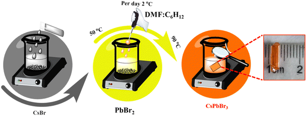 |
| | Scheme 1 Schematic representation of CsPbBr3 single-crystal growth formation. | |
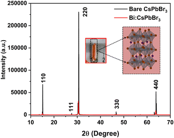 |
| | Fig. 1 Room-temperature X-ray diffraction pattern of CsPbBr3 and Bi-doped CsPbBr3 single crystals. (Inserted image is the single crystal and its crystal structure.). | |
Photo-physical properties of the Bi-doped CsPbBr3 perovskite single crystals
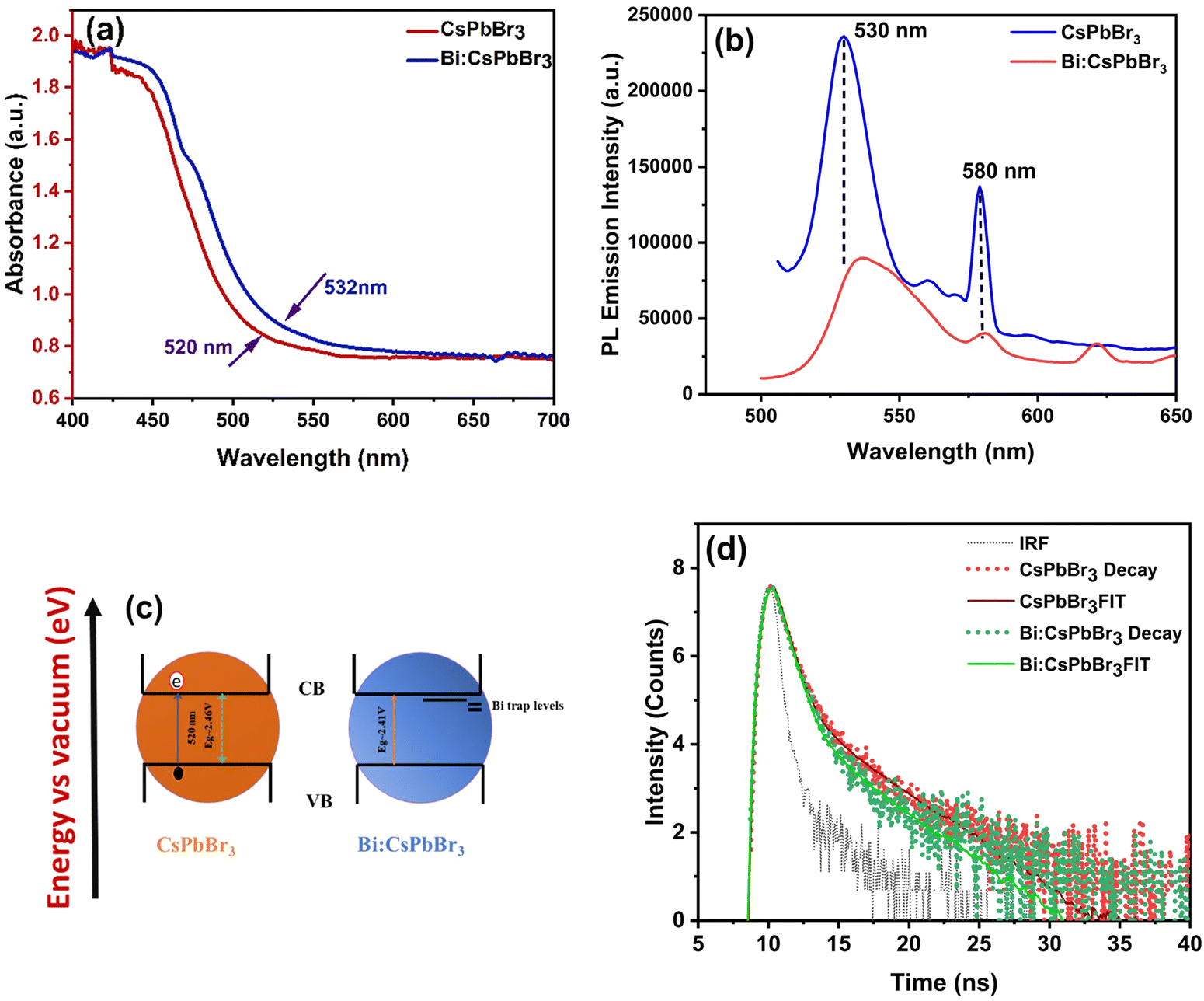
Fig. 2 represents the results obtained from the UV-vis absorption and photoluminescence (PL) emission spectroscopic analyses for CsPbBr3 and Bi-doped CsPbBr3 single crystal samples, respectively. It is observed that there are no distinct peaks in the UV-vis absorption spectrum of both samples. Moreover, the as-prepared CsPbBr3 sample exhibited an absorption onset at 520 nm (Fig. 2a), and the Bi-doped CsPbBr3 sample displayed a slight red-shift around 532 nm. The Tauc plot for the above samples was drawn, and the calculated direct band gap values were 2.4634–36 and 2.41 eV for the pure CsPbBr3 and Bi-doped CsPbBr3 single-crystal samples, respectively37–39 (Fig. S2, ESI†). The observed redshift in the absorption onset and the corresponding decrease in the band gap value are due to the introduction of shallow traps resulting from the Bi doping process.38,40 It has to be noted that the difference in the bandgap values of the corresponding samples is not appreciable, which is due to the lower dopant concentration. Similar observations have been reported for the Bi-doping in CsPbX3 single crystals regardless of the halogen element.19 The photoluminescence emission properties of pure and Bi-doped CsPbBr3 single-crystal samples were studied by recording the PL emission spectrum at an excitation wavelength of 420 nm. As illustrated in Fig. 2b, the pure CsPbBr3 single crystal exhibited two sharp peaks at 530 and 580 nm, which are attributed to the band edge and Br vacancy centre-based recombination, respectively, as reported elsewhere.36,41 The broadening of the PL emission peak at 530 nm along with a slight red-shift in the case of Bi-doped single crystal is attributed to the introduction of shallow traps during the doping process. This observation is in accordance with the UV-vis absorption analysis of the corresponding sample. The introduction of trap states is schematically depicted in Fig. 2c.
 |
| | Fig. 2 (a) UV-vis absorbance spectrum, (b) photoluminescence emission spectrum, (c) schematic representation of Bismuth trap state formation near the conduction band edge and (d) TCSPC lifetime decay curve of solution-processed grown CsPbBr3 single-crystal and Bi-doped CsPbBr3 samples. | |
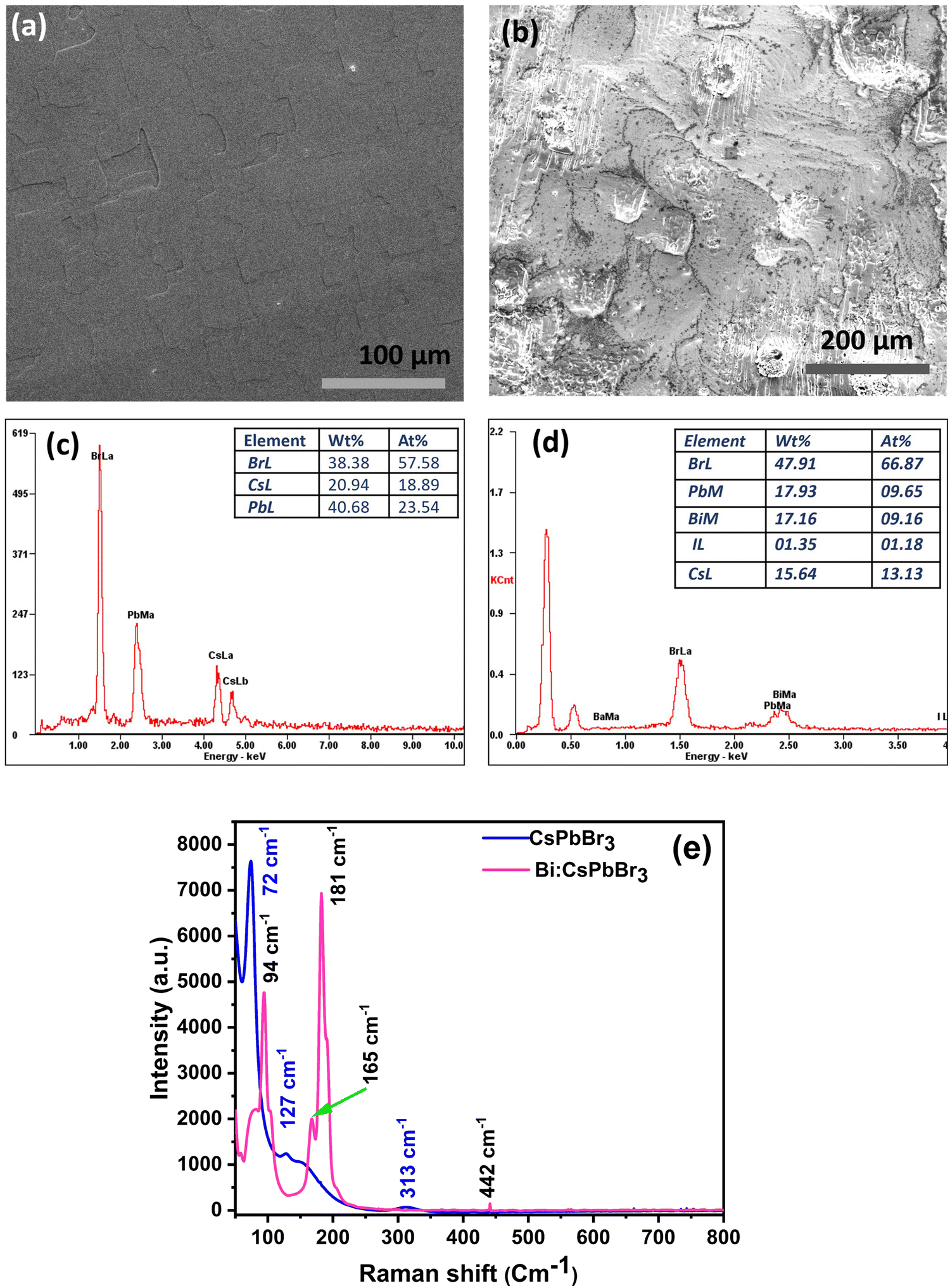
The PL decay curves of the undoped CsPbBr3 and Bi-doped CsPbBr3 single-crystal samples were recorded at their respective emission maxima (at 530 nm) and are shown in Fig. 2d. The average lifetime values are calculated to be 2.67 ns for undoped CsPbBr3, which decreases to 2.25 ns after doping with bismuth. The observed decrease in the PL lifetime values can be attributed to the shallow trap-mediated recombination of photo-excited charge carriers, which is supported by the UV-vis and PL results. Because these shallow traps are introduced inside the band gap near the conduction band edge, a relatively quicker recombination resulted.42 The TCSPC lifetime values of the pure CsPbBr3 and Bi-doped CsPbBr3 single-crystal samples are shown in Table S1 ESI.† The average lifetime value is longer for bare and Bi-doped CsPbBr3 single crystals compared to other nanoparticles and thin films, indicating more efficient extraction of photogenerated electrons. The scanning electron microscopy characterization was carried out, and the micrographs are displayed in Fig. 3a and b. The energy-dispersive X-ray spectroscopy (EDX) elemental graph results of pure CsPBr3 and Bi-doped CsPbBr3 single crystal samples indicate the elemental composition and purity of the corresponding samples (Fig. 3c and d). The Raman spectroscopic analysis was carried out for the CsPBr3 and Bi-doped CsPbBr3 single crystal samples, and the results are shown in Fig. 3e. The pure CsPbBr3 single crystal sample exhibited Raman bands at 72, 127 and 313 cm−1,36 whereas the Bi-doped sample displayed the bands at 94, 165, 181, and 442 cm−1. The vibrational bands at 72 and 94 cm−1 are assigned to the bending mode of the Br–Pb–Br and its antisymmetric partner, respectively.43,44 The peak at 165 cm−1 can be assigned to the symmetric Pb–Br stretching mode, whereas the peak at 127 cm−1 is the asymmetric partner. The bands at 165 cm−1 and 313 cm−1 can be attributed to the liberation of cations involving the deformation of the inorganic cage. The observed vibrational modes of the CsPbBr3 and Bi-doped single crystals elucidated that they are derived mainly from [PbBr6]4− anion.
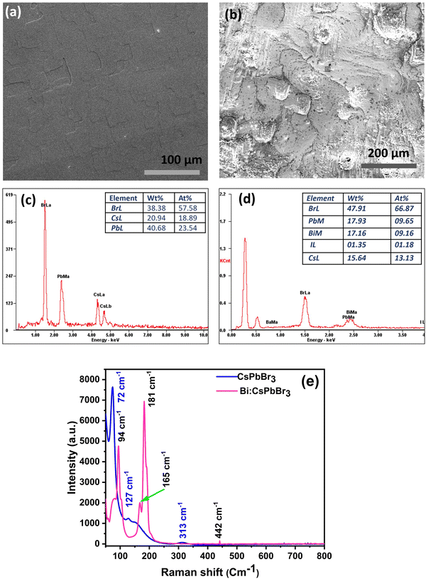 |
| | Fig. 3 (a) and (b) Scanning electron microscopy (SEM) image, (c) and (d) energy-dispersive X-ray spectroscopy (EDX) elemental graph and (e) room-temperature RAMAN spectra (excited at a 785 nm laser) of the CsPbBr3 single crystal and Bi-doped CsPbBr3 samples. | |
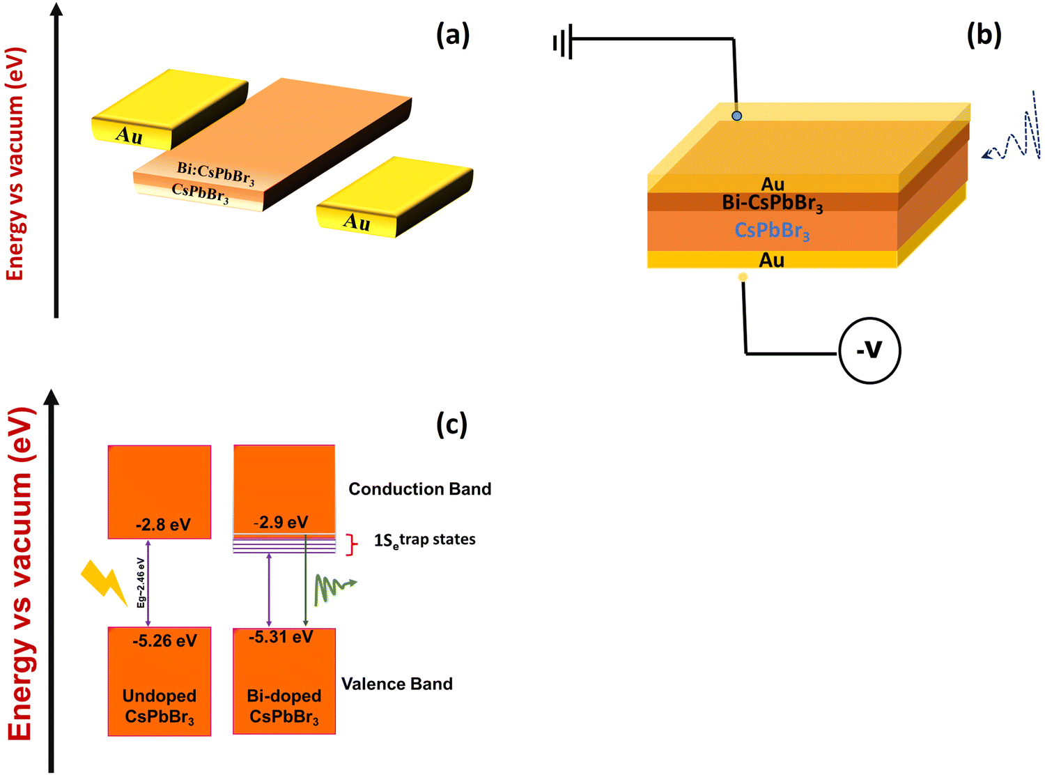
Photocurrent analysis of Bi-doped CsPbBr3 perovskite single crystals
The orthorhombic CsPbBr3 and Bi-doped single crystals were used to construct the photodetector with Au/(Bi-doped) CsPbBr3/Au device structure. The band alignment of CsPbBr3 single crystals with the Au electrode and the schematic diagram of the Bi-doped CsPbBr3 photodetector are shown in Fig. 4a and b, respectively. Fig. 4c depicts the introduction of shallow trap states within the band gap of Bi-doped CsPbBr3, positioned near the bottom of the conduction band edge. The photocurrent measurements were carried out using a low-power illumination of 5 μW to ensure that the light absorption occurred only on the surface of the single crystal. We measured the current–voltage (I–V) characteristics of the undoped CsPbBr3 and Bi-doped CsPbBr3 single-crystal photodetectors in the dark and under light illumination with a bias voltage range of −100 to 100 V. The plots are shown in Fig. 5a and b. The pure CsPbBr3 single crystal showed a dark current value of 0.026 nA for a biasing voltage of 10 V. Upon illumination, the photocurrent increased to 0.83 nA. The Bi-doped CsPbBr3 single crystal produced a dark current value of 0.49 nA for a biasing voltage of 10 V. An interesting increase in the photocurrent value was observed upon illumination. For the same biasing voltage of 10 V, the photocurrent value increased to 5.77 nA. The I–V plots exhibited good linearity in the entire measurement range, thereby indicating that the constructed photodetector devices exhibited good responsivity and sensitivity.
 |
| | Fig. 4 (a) and (b) Schematic representation of the Bi-doped CsPbBr3 photocurrent device and (c) Fermi level and defect state density, valence and conduction band edges by incorporating the bismuth dopant.42,43 | |
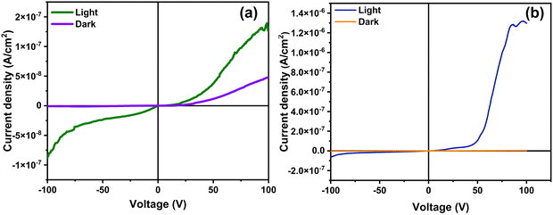 |
| | Fig. 5 (I–V) photocurrent studies of (a) the undoped CsPbBr3 and (b) Bi-doped CsPbBr3 perovskite single crystal. | |
In general, perovskite light absorbers suffer from innumerable complications, such as ion migration, lattice distortion and phase segregation, when subjected to an applied electric field. The absence of such instances in the present case indicates the crystal quality of the samples and resultant resistance to phase change under the applied electric field. Thus, the crystal quality can be indirectly evaluated by analyzing the drift in the dark current of the detectors. The detectors were biased using a high electric field of 100 V, and the resulting dark current was recorded, as demonstrated in Fig. 5b.
X-ray and gamma-ray sensing applications
Introducing perovskite materials in gamma-ray detection is particularly challenging due to the high-voltage accelerated ion migration. The as-prepared Bi-doped CsPbBr3 single crystal was subjected to X-ray and gamma-ray detection. The response characteristics are displayed in Fig. 6a. The Bi-doped CsPbBr3 single crystal responded well to the Cobalt (60Co, energy - 1.25 MeV, activity = 1 μCi) and Cesium (137Cs, energy - 0.662 MeV, activity = 0.93 μCi) sources within the operating voltage ranging from 300 to 600 V, which falls within the GM region, as shown in Fig. 6a. The 60Co produces more particle counts compared to the 137Cs; this is because the 60Co has higher energy and activity than the 137Cs. A portable X-ray characterization study shows a good response to different tube voltages and different tube currents, as shown in Fig. 6b and c. The response of the device was observed as the X-ray tube current varied, which represented the relative dose rate. It was found that the device demonstrated a highly linear response to the variation in the dose rate. This linearity is particularly important for applications in radiation dosimetry. Our recent study showed that the tube voltage ranges from 40 to 100 kV in a unit of 20 kV, and the tube current 122 ranges from 50 to 300 mA in a unit of 50 mA. Fig. 6d shows the mass attenuation coefficients of CsPbBr3, MAPbBr3, MAPbI3 and MAPbCl3 and CZT versus the photon energy according to the XCOM database.45 The increase in tube voltage represents the increase in the number of counts (resulting from the increase in the number of particles). It is therefore clear that the Bi-doped CsPbBr3 single crystal can be used for both X-ray and gamma ray detection and can also be used for high-energy X-ray detection in the future.
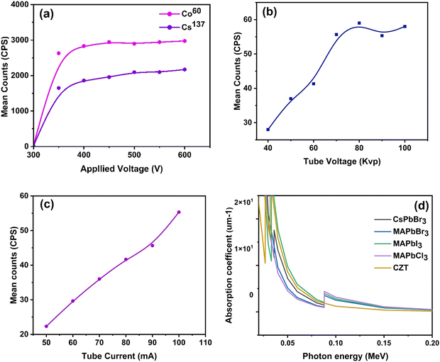 |
| | Fig. 6 Schematic representation of gamma and X-ray detection. (a) Optimization of operating voltage using 60Co and 137Cs. (b) and (c) Characterization at different tube voltages and currents using portable X-ray, and (d) the mass attenuation coefficients of CsPbBr3, MAPbBr3, MAPbI3 and MAPbCl3versus the photon energy according to the XCOM database.45 | |
Photocurrent analysis of Bi-doped CsPbBr3 single crystal thin film
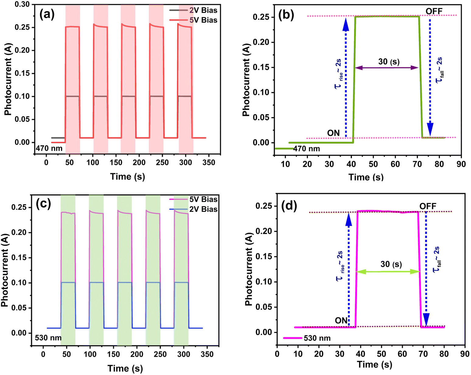
We fabricated Bi-doped CsPbBr3 thin films by dispersing single crystals in DMSO/DMF and spin coating on an FTO substrate. The spin-coated thin films were used to construct photodetectors with FTO/Bi-doped CsPbBr3/Au device structure.46,47 Schematic representation of Bi-doped CsPbBr3 perovskite-based thin-film photodetector fabrication is shown in Fig. S3 (ESI†). The crystallographic characteristics were investigated by XRD characterization. The powder XRD patterns of the CsPbBr3 and Bi-doped CsPbBr3 perovskite thin-film samples on the FTO substrate are shown in Fig. S4 (ESI†). Spectral response curves obtained from the thin-film photodetector study for wavelengths of 470 nm and 530 nm were measured over time at two biasing voltages of 2 V and 5 V. The photocurrent curves in Fig. 7(a–d) show that the prepared thin-film samples exhibit an increase in the photocurrent values as the biasing voltage increases. While irradiating the device with 470 nm and 530 nm light sources, the photocurrent values were observed to be 0.25 mA and 0.20 mA, respectively, for the 5 V bias. The rise and decay time were recorded at an applied bias voltage of 5 V by periodically switching the light ON and OFF at 30-second intervals.
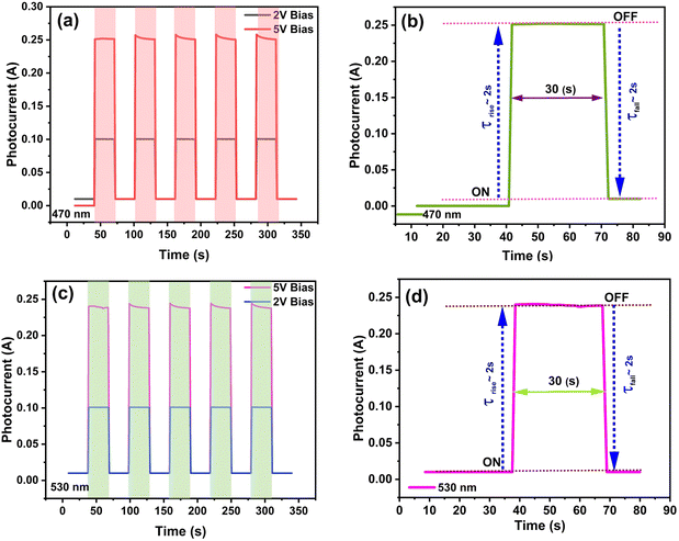 |
| | Fig. 7 (I–V) Photocurrent studies of Bi-doped CsPbBr3 perovskite-based thin-film photodetectors under different light source (a, b) 470 nm and (c, d) 530 nm wavelength at bias 2 V and 5 V. | |
The device exhibited a higher magnitude photocurrent value under a low-intensity power λ = 470 nm LED source with an ON/OFF ratio of Ion/Idark = 596 and for λ = 530 nm LED source, and the ON/OFF ratio was about Ion/Idark ∼24 at 5 V biasing voltage, recording a fast response and recovery time (Table S2, ESI†). The samples tested with low-power intensity illumination are shown in Fig. S5 (ESI†). The calculated responsivity of the Bi-doped CsPbBr3 thin-film perovskite photodetector was 0.35 A W−1. Furthermore, based on the current–voltage curves, the Bi-doped CsPbBr3 thin-film perovskite device demonstrated a better response to blue (470 nm) when compared to the green (530 nm) wavelength. The device maintained good performance after being stored under ambient conditions for over three months.
Conclusions
We successfully demonstrated the synthesis of high-quality Bi-doped CsPbBr3 single crystals by using the ITC solution growth method, and their photophysical properties and sensing were investigated in detail. The photophysical characterization of the CsPbBr3 and Bi-doped CsPbBr3 system and enhancement in the photocurrent measurements were tested with different radioactive sources, and we characterized both X-ray and gamma rays at various activity levels. A portable X-ray characterization study demonstrated an excellent response to different tube voltages and tube currents. This linearity is particularly important for applications in radiation dosimetry. The thin-film-based photodetector results reflected the device performance of the Bi-doped CsPbBr3 thin-film perovskite device, which demonstrated a better response to blue (470 nm) when compared to green (530 nm) wavelength, even after being stored under ambient conditions over three months. Based on the overall performance, the Bi-doped CsPbBr3 perovskite crystal can be used for X-rays and gamma rays. High-energy X-rays can also be detected in the near future using this crystal.
Author contributions
Premkumar Sellan. and Lei Wei conceived the idea. Premkumar Sellan prepared the samples and performed the optical and morphological characterization, and collected the data. Premkumar Sellan conceived the idea for the construction of a photocurrent device. Abida Perveen, Din Nasrud writing review & editing and supporting for samples testing. Manigandan Selvam data curation, Sakthivel Chandrasekar review & editing. Pitchaikannu Venkatraman supporting the characterization of radiation detection, Byung Seong Bae and Damian Chinedu Onwudiwe writing review & editing. Premkumar Sellan and Lei Wei analyzed the collected data and wrote the manuscript and all other authors took part in their respective data analyses.
Data availability
All the related experimental data that support the findings of this research work are accessible from the corresponding author by means of a reasonable request. Some of the experimental results, such as Fig. S1–S5, are provided in the ESI† data file.
Conflicts of interest
There are no conflicts to declare.
Acknowledgements
This work is financially supported by International cooperative research project of Jiangsu province (BZ2022008), National Key Research and Development Program of China (2022YFE0139100), National Natural Science Foundation Project of China (62175028), Program 111_2.0 in China (BP0719013).
Notes and references
- F. Liu,
et al., Recent Progress in Halide Perovskite Radiation Detectors for Gamma-Ray Spectroscopy, ACS Energy Lett., 2022, 7, 1066–1085 CrossRef CAS.
- J. S. Iwanczyk, W. F. Schnepple and M. J. Masterson, The effect of charge trapping on the spectrometric performance of HgI2 gamma-ray detectors, Nucl. Instrum. Methods Phys. Res., Sect. A, 1992, 322, 421–426 CrossRef.
- H. L. Malm, T. W. Raudorf, M. Martini and K. R. Zanio, Gamma Ray Efficiency Comparisons for Si(Li), Ge, CdTe and HgI2 Detectors, IEEE Trans. Nucl. Sci., 1973, 20, 500–509 CAS.
- M. Partridge, B.-M. Hesse and L. Müller, A performance comparison of direct- and indirect-detection flat-panel imagers, Nucl. Instrum. Methods Phys. Res., Sect. A, 2002, 484, 351–363 CrossRef CAS.
- D. V. Kalaga,
et al., Some industrial applications of gamma-ray tomography, J. Taiwan Inst. Chem. Eng., 2009, 40, 602–612 CrossRef CAS.
- L. Protesescu,
et al., Nanocrystals of Cesium Lead Halide Perovskites (CsPbX 3, X = Cl, Br, and I): Novel Optoelectronic Materials Showing Bright Emission with Wide Color Gamut, Nano Lett., 2015, 15, 3692–3696 CrossRef CAS PubMed.
- X. Geng,
et al., Lead-Free Halide Perovskites for Direct X-Ray Detectors, Adv. Sci., 2023, 10, 2300256 CrossRef CAS PubMed.
- H. Wei and J. Huang, Halide lead perovskites for ionizing radiation detection, Nat. Commun., 2019, 10, 1066 CrossRef PubMed.
- L. Zhao,
et al., High-yield growth of FACsPbBr3 single crystals with low defect density from mixed solvents for gamma-ray spectroscopy, Nat. Photonics, 2023, 17, 315–323 CrossRef CAS.
- R. J. Cooper, M. Amman and K. Vetter, High resolution gamma-ray spectroscopy at high count rates with a prototype High Purity Germanium detector, Nucl. Instrum. Methods Phys. Res., Sect. A, 2018, 886, 1–6 CrossRef CAS.
- A. J. Tavendale, Large Germanium Lithium-Drift p-i-n Diodes for Gamma-Ray Spectroscopy, IEEE Trans. Nucl. Sci., 1965, 12, 255–264 CAS.
- R. Gupta,
et al., Synthesis and characterization of all-inorganic (CsPbBr3) perovskite single crystals, Mater. Adv., 2022, 3, 7865–7871 RSC.
- Y. Feng,
et al., Low defects density CsPbBr3 single crystals grown by an additive assisted method for gamma-ray detection, J. Mater. Chem. C, 2020, 8, 11360–11368 RSC.
- J. Kang and L. W. Wang, High Defect Tolerance in Lead Halide Perovskite CsPbBr3, J. Phys. Chem. Lett., 2017, 8, 489–493 CrossRef CAS PubMed.
- Y. Eisen, A. Shor and I. Mardor, CdTe and CdZnTe gamma ray detectors for medical and industrial imaging systems, Nucl. Instrum. Methods Phys. Res., Sect. A, 1999, 428, 158–170 CrossRef CAS.
- Y. Eisen, A. Shor and I. Mardor, CdTe and CdZnTe X-ray and gamma-ray detectors for imaging systems, IEEE Trans. Nucl. Sci., 2004, 51, 1191–1198 CAS.
-
K. Lee
et al.
, Development of x-ray and gamma-ray CZT detectors for homeland security applications, ed. R. S. Harmon, J. H. Holloway Jr. & J. T. Broach, 2010, 766423 DOI:10.1117/12.850113.
- C. Szeles, CdZnTe and CdTe materials for X-ray and gamma ray radiation detector applications, Phys. Status Solidi B, 2004, 241, 783–790 CrossRef CAS.
- E. Jedlicka,
et al., Bismuth Doping Alters Structural Phase Transitions in Methylammonium Lead Tribromide Single Crystals, J. Phys. Chem. Lett., 2021, 12, 2749–2755 CrossRef CAS PubMed.
- P. K. Nayak,
et al., Impact of Bi 3+ Heterovalent Doping in Organic–Inorganic Metal Halide Perovskite Crystals, J. Am. Chem. Soc., 2018, 140, 574–577 CrossRef CAS PubMed.
- O. A. Lozhkina,
et al., Invalidity of Band-Gap Engineering Concept for Bi3+ Heterovalent Doping in CsPbBr3 Halide Perovskite, J. Phys. Chem. Lett., 2018, 9, 5408–5411 CrossRef CAS PubMed.
- J. Peng,
et al., Crystallization of CsPbBr3 single crystals in water for X-ray detection, Nat. Commun., 2021, 12, 1531 CrossRef CAS PubMed.
- J. Ma, T. J. Miao and J. Tang, Charge carrier dynamics and reaction intermediates in heterogeneous photocatalysis by time-resolved spectroscopies, Chem. Soc. Rev., 2022, 51, 5777–5794 RSC.
- M. Sebastian,
et al., Excitonic emissions and above-band-gap luminescence in the single-crystal perovskite semiconductors CsPbBr3 and CsPbCl3, Phys. Rev. B: Condens. Matter Mater. Phys., 2015, 92, 235210 CrossRef.
- M. I. Saidaminov,
et al., High-quality bulk hybrid perovskite single crystals within minutes by inverse temperature crystallization, Nat. Commun., 2015, 6, 7586 CrossRef PubMed.
- Y. Rakita,
et al., Low-Temperature Solution-Grown CsPbBr3 Single Crystals and Their Characterization, Cryst. Growth Des., 2016, 16, 5717–5725 CrossRef CAS.
- S. Premkumar, D. Nataraj, G. Bharathi, S. Ramya and T. D. Thangadurai, Highly Responsive Ultraviolet Sensor Based on ZnS Quantum Dot Solid with Enhanced Photocurrent, Sci. Rep., 2019, 9, 18704 CrossRef CAS PubMed.
- S. Premkumar, D. Nataraj, G. Bharathi, O. Y. Khyzhun and T. D. Thangadurai, Interfacial Chemistry-Modified QD-Coupled CdTe Solid Nanowire and Its Hybrid with Graphene Quantum Dots for Enhanced Photocurrent Properties, ChemistrySelect, 2017, 2, 10771–10781 CrossRef CAS.
- Y. Wang,
et al., Epitaxial Growth of Large-Scale Orthorhombic CsPbBr3 Perovskite Thin Films with Anisotropic Photoresponse Property, Adv. Funct. Mater., 2019, 29, 1904913 CrossRef CAS.
- M. Li, X. Zhang, K. Matras-Postolek, H.-S. Chen and P. Yang, An anion-driven Sn2+ exchange reaction in CsPbBr 3 nanocrystals towards tunable and high photoluminescence, J. Mater. Chem. C, 2018, 6, 5506–5513 RSC.
- Ch. K. Møller, Crystal Structure and Photoconductivity of Caesium Plumbohalides, Nature, 1958, 182(4647), 1436 CrossRef.
- R. Gupta,
et al., Synthesis and characterization of all-inorganic (CsPbBr3) perovskite single crystals, Mater. Adv., 2022, 3, 7865–7871 RSC.
- J. Zhang,
et al., n-Type Doping and Energy States Tuning in CH3NH3Pb1–xSb2x/3I3 Perovskite Solar Cells, ACS Energy Lett., 2016, 1, 535–541 CrossRef CAS.
- H. Lan,
et al., All-inorganic CsPbBr3 thin-film solar cells prepared by single-source physical vapor deposition, Mater. Sci. Semicond. Process., 2021, 132, 105869 CrossRef CAS.
- Y. He,
et al., High spectral resolution of gamma-rays at room temperature by perovskite CsPbBr3 single crystals, Nat. Commun., 2018, 9, 1609 CrossRef PubMed.
- X. Wei,
et al., Low-temperature architecture of a cubic-phase CsPbBr3 single crystal for ultrasensitive weak-light photodetectors, Chem. Commun., 2021, 57, 7798–7801 RSC.
- R. Gupta,
et al., Synthesis and characterization of all-inorganic (CsPbBr3) perovskite single crystals, Mater. Adv., 2022, 3, 7865–7871 RSC.
- O. A. Lozhkina,
et al., Invalidity of Band-Gap Engineering Concept for Bi3+ Heterovalent Doping in CsPbBr3 Halide Perovskite, J. Phys. Chem. Lett., 2018, 9, 5408–5411 CrossRef CAS PubMed.
- R. Wang,
et al., Bi3+-doped CH3NH3PbI3: Red-shifting absorption edge and longer charge carrier lifetime, J. Alloys Compd., 2017, 695, 555–560 CrossRef CAS.
- X. Zhang,
et al., All-Inorganic Perovskite Nanocrystals for High-Efficiency Light Emitting Diodes: Dual-Phase CsPbBr3-CsPb2Br5 Composites, Adv. Funct. Mater., 2016, 26, 4595–4600 CrossRef CAS.
- M. Chen, Y. Yuan, Y. Liu, D. Cao and C. Xu, High-quality all-inorganic CsPbBr3 single crystals prepared by a facile one-step solution growth method, RSC Adv., 2022, 12, 14838–14843 RSC.
- V. Naresh, T. Jang, Y. Pang and N. Lee, Highly luminescent dual-phase CsPbBr3/Cs4PbBr6 microcrystals for a wide color gamut for backlight displays, Nanoscale, 2022, 14, 17789–17801 RSC.
- S. Ghosh,
et al., Vibrational study of lead bromide perovskite materials with variable cations based on Raman spectroscopy and density functional theory, J. Raman Spectrosc., 2021, 52, 2338–2347 CrossRef CAS.
-
O. Yaffe
et al.
, in The nature of dynamic disorder in lead halide perovskite crystals (Conference Presentation), ed. Bakulin, A. A., Banerji, N. & Lovrincic, R., Physical Chemistry of Interfaces and Nanomaterials XV 48, SPIE, 2016 DOI:10.1117/12.2236330.
-
M. J. Berger
et al.
, XCOM: Photon Cross Sections Database: NIST Standard Reference Database 8, NIST, 2013, 2013 Search PubMed.
- S. Premkumar,
et al., Stable Lead-Free Silver Bismuth Iodide Perovskite Quantum Dots for UV Photodetection, ACS Appl. Nano Mater., 2020, 3, 9141–9150 CrossRef CAS.
- S. Premkumar,
et al., Ag2BiI5 Perovskite Quantum Dots Passivated with Oleylamine Sulfide for Solar Cells and Detection of Cu(II) Ions, ACS Appl. Nano Mater., 2021, 4, 9895–9903 CrossRef CAS.
|
| This journal is © The Royal Society of Chemistry 2024 |
Click here to see how this site uses Cookies. View our privacy policy here. 
 Open Access Article
 This Open Access Article is licensed under a Creative Commons Attribution-Non Commercial 3.0 Unported Licence
 *a,
Manigandan
Selvan
b,
Abida
Perveen
a,
Din
Nasrud
a,
Sakthivel
Chandrasekar
c,
Pitchaikannu
Venkatraman
d,
Devaraj
Nataraj
*a,
Manigandan
Selvan
b,
Abida
Perveen
a,
Din
Nasrud
a,
Sakthivel
Chandrasekar
c,
Pitchaikannu
Venkatraman
d,
Devaraj
Nataraj