 Open Access Article
Creative Commons Attribution 3.0 Unported Licence
Binder polymer influence on the electrical and UV response of organic field-effect transistors†
Jinghai Li‡
a,
Adrián Tamayo‡a,
Aleix Quintanaa,
Sergi Riera-Galindoa,
Raphael Pfattner a,
Yanyan Gongab and
Marta Mas-Torrent
 *a
*a
aInstitut de Ciència de Materials de Barcelona, ICMAB-CSIC, Campus UAB, 08193 Bellaterra, Cerdanyola, Spain. E-mail: mmas@icmab.es
bState Key Laboratory of Biobased Material and Green Papermaking, Qilu University of Technology (Shandong Academy of Sciences), Jinan, 250353, P. R. China
First published on 30th January 2023
Abstract
The use of blends of small molecule organic semiconductors (OSCs) with insulating binding polymers has been shown to be a promising route to facilitate the processing of OSCs over large areas using printing techniques. Here we fabricated organic field-effect transistors (OFETs) and phototransistors using the benchmark OSC 7-decyl-2-phenyl[1]benzothieno[3,2-b][1]benzothiophene (Ph-BTBT-10) and blends of this material with polystyrene (PS), poly(pentafluorostyrene) (PFS) and poly(methyl methacrylate) (PMMA). We show that the nature of the binding polymer has a significant impact on the device performance. The OFETs showing the best performance are the ones based on blends of PS since they reveal less interfacial traps, leading to devices with higher mobility, threshold voltage close to zero and high bias stress stability. The lowest OFET performance is found in the devices based on PMMA blends due to the higher density of majority charge carrier (i.e., holes) traps. On the other hand, regarding the response of the devices to UV light, the PFS and pristine films exhibited the highest photoresponse, which was attributed to the higher density of minority charge carrier (i.e., electrons) traps. Therefore, this work demonstrates that the binding polymer is a useful tool to optimise the OFET electrical characteristics as well as its photoresponsivity.
10th Anniversary StatementThe Journal of Materials Chemistry and, subsequently, the Journal of Materials Chemistry C, has always been one of our priority journals in our research group to publish our latest results on the preparation of new materials and devices as well as on their electrical characterization. This journal has a good balance of work reporting fundamental studies, such as structure–property correlation studies, that are combined with more applied investigations. We also had the chance to contribute with several Highlight papers, which we believe provide an overview of current recent research tendencies in materials science in a concise way. |
Introduction
The development of printing techniques compatible with roll-to-roll processes to deposit organic semiconductors (OSCs) is key for the progress and implementation of organic electronic devices, such as organic field-effect transistors (OFETs).1–4 Small molecule OSCs can be easily purified and can form more ordered crystalline thin films than polymers. However, the preparation of homogenous thin films of small molecule OSCs employing printing techniques can be challenging due to the limited solubility of these materials, their poor stability under ambient conditions and dewetting problems caused by the low viscosity of their solutions.5–8 This can be mainly circumvented by blending the OSCs with insulating binding polymers.9,10 The use of blends has been shown to enhance the thin film processability, crystallinity and environmental stability.9,11–14 In addition, the use of binding polymers can provide an additional tool to tune the device properties.15,16 In fact, binding polymers have been exploited to control the diffusion of dopants, stabilise metastable polymorphs and reduce interfacial traps.17–20Wide ranging opportunities for OFETs are open in sensing applications since they can provide a multi-parametric electric response to physical or chemical changes in the environment with high sensitivity. In particular, OFETs are promising platforms for developing light detectors (i.e., phototransistors). Photodetectors convert light into an electrical signal and have relevant technological applications in biomedical imaging, sensing, optical communication and environmental monitoring.21–24 The use of OFETs as photodetectors offers the possibility of detection wavelength tuneability, low-cost manufacturing, and compatibility with flexible substrates.25–27 For instance, photodetectors with high sensitivity in the UV range but negligible response in the visible range are desired in applications such as health care, chemical and pollutant sensing, combustion and flame detection, military applications and radiation detection.28 Traditional UV detectors often require filters or waveguides to separate UV from visible light, increasing the device complexity.29 Hence, OSCs that only absorb in the UV region can represent an appealing low-cost alternative for some applications.
When an incident photon is absorbed by the OSC an exciton is created and it diffuses through the OSC until it reaches a trap (i.e., localised electronic state in the OSC band gap created by chemical impurities, structural disorder, interfacial or environmental effects, etc.)29 that dissociates it into an electron and a hole. By trapping and de-trapping the minority or majority charge carriers, the recombination rate is reduced, increasing one kind of carrier concentration.30 This can lead to an increase in the phototransistor current and a shift of the threshold voltage. Charges can be trapped at intrinsic defects at the semiconductor channel or at the OSC/dielectric interface.25 Therefore, it is possible to manipulate the charge trapping process and thus the photoresponse, by modifying the thin film morphology and interfaces.31–33
In this study, we fabricated OFETs based on blends of the high performing p-type OSC 7-decyl-2-phenyl[1]benzothieno[3,2-b][1]benzothiophene (Ph-BTBT-10, Fig. 1) with different binding polymers and investigated the effect of these blends on the OFET performance as well as on the device photoresponsivity to UV light. Binding polymers have been employed as a tool to improve the OSC processability and to achieve more homogenous thin films. In addition, it is known that binding polymers also have an effect on the device characteristics.34–37 Here, it was found that the nature of the binding polymer influences the trap density of majority and minority charge carriers. The best OFET performance is found in the blend films exhibiting a lower level of traps, while the worst performance is encountered in the films with a higher level of majority charge carrier traps. In contrast, the optimum photoresponse is revealed by the films exhibiting a higher density of minority charge carrier traps. Therefore, this work demonstrates that the binding polymer is a useful tool to tune and optimise the device properties.
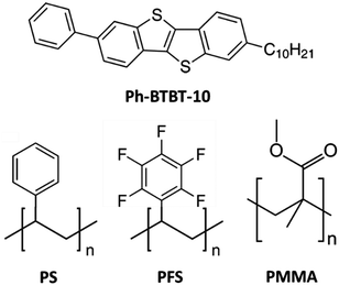 | ||
| Fig. 1 Chemical structures of the employed small molecule organic semiconductor (top) and the binding polymers (bottom). | ||
Results and discussion
The OSC Ph-BTBT-10 was selected due to the fact that it is soluble in organic solvents and, hence can be processed from solution, exhibits a high mobility and, further, in the solid state, it absorbs in the UV region of 330–390 nm (maximum at 363 nm Fig. S1a, ESI†) but is transparent in the visible region.38,39 Thus, this OSC is a promising OSC to detect UV light.40,41Thin films of Ph-BTBT-10 and blends of this material with polystyrene (PS), poly(pentafluorostyrene) (PFS) and poly(methyl methacrylate) (PMMA) were deposited using the bar-assisted meniscus shearing (BAMS) technique on Si/SiO2 substrates, employing the same deposition conditions as previously reported (see the Experimental section10,13,42,43). The use of binding polymers typically gives rise to a vertical phase separation, where, commonly, the OSC crystallises on top of a layer of the binding polymer. The nature of the binding polymer though can influence this phase separation and the crystallisation of the OSC at the interface. Noticeably, none of these binding polymers absorb light in the UV-Vis region above 320 nm (Fig. S1b, ESI†).
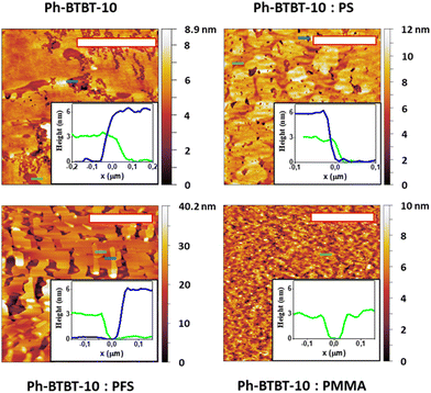
The optical polarised microscope images of the thin films revealed a polycrystalline structure with small crystal domains for all blends (Fig. S2, ESI†). In addition, the films were characterised by atomic force microscopy (AFM) (Fig. 2). All the thin films are around 20 nm thick and show a very low roughness in the range 2–6 nm (Table S1, ESI†). The nature of the binding polymer results in thin films with different morphology. In the case of PFS-based films, more incomplete molecular layers are formed and thus more terraces are observed. It should be also noticed that the crystalline domains are much smaller in the PMMA blend films in comparison with the other ones. Furthermore, steps of around 2.9 ± 0.2 and 5.9 ± 0.3 nm high are observed in all the cases, which correspond to an extended molecular monolayer and bilayer, respectively. This is indicative that the OSC is crystallising on the top part of the films, as previously observed (inset Fig. 2).38,42
The films were also investigated by X-ray diffraction (XRD). All samples displayed the same XRD pattern as the one previously reported for Ph-BTBT-10 films, which corresponds to a herringbone packing (Fig. S3, ESI†).38,42,44 Only the (00l) reflections are discernible, indicating that the molecules are preferentially oriented with the ab plane parallel to the substrate. Comparing the position of the first (001) peak, small shifts can be distinguished, which might be indicative of some lattice strain caused by different binding polymers.45,46
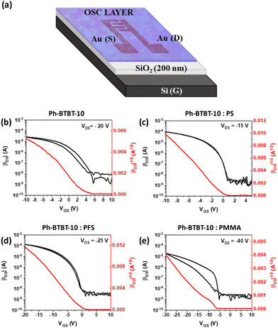
The OSC thin films were investigated as an active layer in OFETs, in a bottom gate bottom contact structure, with the aim of exploring how the binder polymer affects their electrical performance (see Fig. 3a for the device configuration). The transfer characteristics for all the devices in the saturation regime are shown in Fig. 3b–e (see Fig. S4 for the output characteristics, ESI†), and the parameters extracted are collected in Table 1.
| Ink formulation | Pristine | PS | PFS | PMMA |
|---|---|---|---|---|
| a The photoresponsivity measurements were carried out under a light power of 486 μW cm−2 and an active area of 2.5 × 10⁻³ cm2. The photocurrent value was extracted at VDS = −1 V and at VGS = VON of the device without UV exposure. The OFET parameters are averaged from 20 different devices, while the photoresponse parameters correspond to the average of 3 devices. | ||||
| Mobility (cm2 V−1 s−1) | 0.33 ± 0.08 | 1.2 ± 0.1 | 0.41 ± 0.10 | 0.10 ± 0.05 |
| Threshold Voltage (V) | 2 ± 1 | −0.2 ± 0.9 | 2 ± 2 | −7 ± 1 |
| Nt(eV−1 cm2) | (2.5 ± 0.4) × 1012 | (9.3 ± 0.7) × 1011 | (1.9 ± 0.6) × 1012 | (4.1 ± 0.9) × 1012 |
| β | 0.61 ± 0.01 | 0.55 ± 0.01 | 0.74 ± 0.02 | 0.78 ± 0.02 |
| τ (s) | (3.6 ± 0.1) × 103 | (1.9 ± 0.1) × 104 | (4.5 ± 0.1) × 103 | (7.9 ± 0.1) × 103 |
| Photoresponsivity (mA W−1)a | (3.2 ± 0.3) × 102 | (2.0 ± 0.4) × 10 | (3.9 ± 0.3) × 102 | (3.7 ± 0.9) × 10 |
The devices exhibit p-type OFET behaviour. The transfer characteristics show lower hysteresis when the OSC is blended with PS and PFS compared to the devices based on only the pristine OSC. However, the OFETs based on Ph-BTBT-10 blended with PMMA clearly reveal an enhanced hysteresis, which can be caused by the hole trapping effect of the polar ester groups of this polymer.47–49 The devices based on blends of PS show average threshold voltage values (Vth) close to zero, while the ones based on the pristine OSC and blends of PFS show values slightly positively shifted (+2 V) and the blends with PMMA show higher negative Vth values (i.e., −7 V). Positive Vth values are indicative of some unintentional doping, which can be caused by water from the environment in the case of pristine films and it has also been previously observed in blends based on fluorinated polymers due to p-doping of the OSC caused by the strong dipole moments of C–F bonds.46,50 On the other hand, the negative Vth value found in the PMMA blend is attributed to charge trapping at the interface, which hinders the switching on of the OFET. Finally, PS blends give rise to devices less doped and with lower interfacial traps, as previously observed with a variety of OSCs, which was ascribed to the passivation of the SiO2 dielectric that prevents water penetration.12,13,17,21,51 Indeed, the interfacial hole trap densities (Nt) have been estimated from the sub-threshold swing (SS). In agreement with the previous observations, PMMA films exhibit the higher density of hole-traps, while the PS films the lowest one (Table 1).
Taking into account the field effect mobility, the highest value is found with the PS blend with an average mobility of 1.2 ± 0.1 cm2 V−1 s−1. The pristine and PFS blends achieve mobility values of 0.33 ± 0.08 and 0.41 ± 0.10 cm2 V−1 s−1, respectively. Finally, the PMMA blends show the lowest mobility (i.e., 0.10 ± 0.05 cm2 V−1 s−1), which can be partly due to the lower size of the crystalline domains and the higher hole trap density. It should also be noticed that often the films based on PMMA show a double slope in the mobility extraction. In previous works, the use of PMMA in similar films gave analogous results (i.e., films with lower crystal domains and reduced performance).49
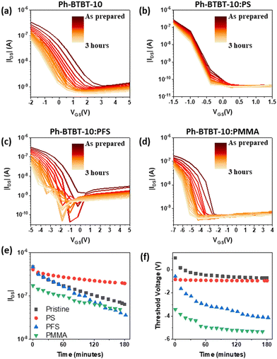
The operational stability of the OFETs was explored in a dark and ambient atmosphere (50 ± 5% humidity). The bias stress stability in OFETs is determined by the interfacial traps but also by other factors such as the grain sizes (i.e., the thin film morphology).52,53 The bias stress tests consisted in the application of a drain voltage VDS= −1 V and gate voltages (VGS) giving similar source-drain current (IDS) (pristine: VGS = −7 V; PS blend: VGS = −2 V; PFS blend: VGS = −5 V; PMMA blend: VGS = −9 V), and measuring the transfer characteristics in the linear regime (VDS= −1 V) every 10 minutes for 3 hours (Fig. 4). Clearly, it is observed that the most operationally stable device is the one based on the PS blend, where the recorded transfer curves are almost overlapping. In contrast, in the pristine films and in the other blends a significant shift of Vth is taking place during the test.
The IDS decay caused by the bias stress was fitted with the following eqn (1), which relates the IDS decay with the concentration of traps:54–56
 | (1) |
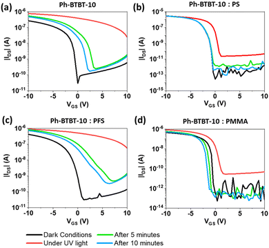
Subsequently, the electrical photoresponse of the devices under UV light was measured. A UV LED with a spectral output centred at 375 nm, close to the maximum of Ph-BTBT-10 absorbance, was employed as the light source, which was calibrated using a power meter to determine light intensity (Fig. S5, ESI†). In Fig. 5 the transfer characteristic plots of the devices before and upon exposition to the UV light are shown. Furthermore, the recovery curves after the light exposition are also plotted in the same figure.
It can be observed that a large increase in the off current and a significant shift of the Vth towards positive values is observed in the pristine and PFS blend films.57–60 This implies an enhancement in the majority of charge carriers (i.e., holes).25,59 Notice that the leakage gate current under illumination is two orders of magnitude lower (Fig. S6, ESI†). In the films based on PMMA and PS this phenomenon is much less pronounced. In addition, in these latter films the transfer characteristics recover their initial source-drain current values quickly after irradiation, which does not occur in the pristine and PFS blend devices.
The photoresponsivity (R), defined as the photocurrent (Ilight − Idark) generated by unit of optical power density of the incident light (P) (eqn (2)), was calculated for all the films (Table 1).
 | (2) |
The highest photoresponse was found for the Ph-BTBT-10 (P = (3.2 ± 3) × 102 mA W−1) and Ph-BTBT-10:PFS films (P = (3.9 ± 3) × 102 mA W−1). These values were two orders of magnitude higher than the one found for the PMMA-based films, while the PS blends showed an intermediate response. In the case of the pristine films, the hydroxyl groups of the SiO2 dielectric are known to act as electron traps.61 Regarding the PFS blends, the effect of the dipole groups could also lead to electron trapping.50,62,63 Thus, the interfacial electron trap density induced by the PFS binder polymer or the SiO2 interface boosts the photoresponse of the OFETs. This is due to the fact that when the generated excitons are dissociated, the electrons are trapped, reducing the hole–electron recombination and increasing the measured hole source-drain current. In contrast, the lower response of the PMMA films can be explained by the fact that, as previously mentioned, the ester groups of the polymer act as trapping sites for holes and, therefore, the increase of measured current is less noticeable.33
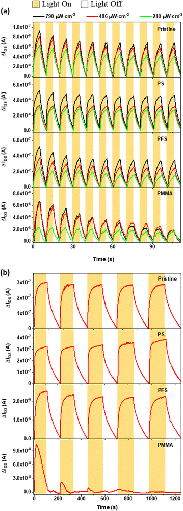
The dynamic photoresponse of all the prepared OFETs was evaluated by monitoring the IDS as a function of time under three different powers of UV illumination (210, 486 and 790 μW cm−2). Fig. 6a shows the dynamic photoresponse behaviour for a short illumination pulse time of 5 s with recovery periods of also 5 s. Notice that in these measurements the devices were in the ON state: VDS was kept at −1 V and, in order to have a similar initial IDS (i.e., 1 μA), the applied VGS for the pristine, PS, PFS and PMMA blends were −4.5, −1, −0.7 and −11 V, respectively. In all the cases, after illumination an increase in IDS is observed, which tends to recover when the light is switched off. As expected, the increase in current is greater when more power light is applied. It is observed that with time the PMMA films respond less to light. This is more clearly visualised when performing longer light pulses (110 s of light exposition and recovery), as shown in Fig. 6b. Therefore, it is demonstrated that the PMMA blends not only show a lower photoresponse but they also exhibit a very poor photostability.
Experimental section
Materials
Ph-BTBT-10 was purchased from TCI chemicals, PMMA (25![[thin space (1/6-em)]](https://www.rsc.org/images/entities/char_2009.gif) 000 g mol−1) from Polysciences, Inc., and PS (Mw 280
000 g mol−1) from Polysciences, Inc., and PS (Mw 280![[thin space (1/6-em)]](https://www.rsc.org/images/entities/char_2009.gif) 000 g mol−1), PFS (polydisperse), 2,3,4,5,6-pentafluorothiophenol (PFBT, 97%) and o-xylene (≥99.5%) were purchased from Sigma-Aldrich. All the materials were used as received.
000 g mol−1), PFS (polydisperse), 2,3,4,5,6-pentafluorothiophenol (PFBT, 97%) and o-xylene (≥99.5%) were purchased from Sigma-Aldrich. All the materials were used as received.
Device fabrication
Interdigitated evaporated source and drain electrodes (Cr (5 nm) and Au (40 nm)) were fabricated by photolithography on a heavily n-doped Si wafer (Si-Mat) with a 200 nm oxide layer. The channel length and width were fixed at 50 μm and 5000 μm, respectively. The substrates were cleaned in an ultrasonic bath with acetone and isopropanol and then dried under nitrogen flow. The gold surface of the source and drain electrodes was then chemically modified with a self-assembled monolayer of PFBT. The substrates were first cleaned using ultraviolet ozone for 25 min, and were then immersed in a 10−3 M solution of PFBT in isopropanol for 15 minutes. Afterwards, the substrates were rinsed with isopropanol and dried with nitrogen.Pristine Ph-BTBT-10 and blend solutions of Ph-BTBT-10 with PMMA, PFS and PS at a weight ratio of 2![[thin space (1/6-em)]](https://www.rsc.org/images/entities/char_2009.gif) :
:![[thin space (1/6-em)]](https://www.rsc.org/images/entities/char_2009.gif) 1 were dissolved in o-xylene (2.5 wt%). Previously to their deposition, all solutions were heated at 105 °C. The active layers were deposited on the substrates using the BAMS technique at 10 mm s−1 and at a substrate temperature of 105 °C, using home-designed equipment.10,13,19,42 Note that all the fabrication process was carried out under ambient conditions and no post-thermal treatments were required.
1 were dissolved in o-xylene (2.5 wt%). Previously to their deposition, all solutions were heated at 105 °C. The active layers were deposited on the substrates using the BAMS technique at 10 mm s−1 and at a substrate temperature of 105 °C, using home-designed equipment.10,13,19,42 Note that all the fabrication process was carried out under ambient conditions and no post-thermal treatments were required.
Electrical measurements
The electrical measurements were performed under ambient conditions using an Agilent B1500A semiconductor devices analyser connected to the samples with a Karl Suss probe station. The UV light system was a home-made setup with an UV LED (LED370E from ThorLabs) with a spectra intensity distribution centred at λ = 370 nm (power information shown in the ESI† Fig. S4). An opaque box to shade the ambient light was used. Transfer characteristics were measured in the saturation regime. The mobility and threshold voltage were extracted in the saturation regime using eqn (3):
 | (3) |
The interfacial trap density per unit area (NT) was estimated using the relationship (eqn (4)):
 | (4) |
Thin-film characterisation
Optical microscope images were taken using an Olympus BX51 equipped with a polariser and analyser. X-ray diffraction measurements were carried out with a Siemens D-50![[thin space (1/6-em)]](https://www.rsc.org/images/entities/char_2009.gif) 000 diffractometer. The Cu K radiation used was 1.54187 Å. Atomic Force Microscopy (AFM) images were taken with a 5100 and 5500LS SPM system from Agilent Technologies. Surface topography and film thickness were examined using a 5500LS SPM system from Agilent Technologies and subsequent data analysis was performed by using Gwyddion 2.61 software. The absorption spectrum of the polymer solutions and the OSC thin films prepared on quartz substrates were measured using a UV-visible Jasco spectrophotometer (V-780) on films.
000 diffractometer. The Cu K radiation used was 1.54187 Å. Atomic Force Microscopy (AFM) images were taken with a 5100 and 5500LS SPM system from Agilent Technologies. Surface topography and film thickness were examined using a 5500LS SPM system from Agilent Technologies and subsequent data analysis was performed by using Gwyddion 2.61 software. The absorption spectrum of the polymer solutions and the OSC thin films prepared on quartz substrates were measured using a UV-visible Jasco spectrophotometer (V-780) on films.
Conclusions
In summary, in this work we fabricated thin films of the OSC Ph-BTBT-10 and blends of this material with three different binding polymers: PS, PFS and PMMA. The Ph-BTBT-10 OSC was selected since it exhibits a high hole mobility, it can be processed from solution and is absorbed in the UV region, thus being a promising material for the development of UV-photodetectors.It was observed that the nature of the binding polymer has a dramatic effect on the electrical OFET properties. The films based on PS exhibited the best performance, showing the highest mobility, a Vth close to zero, a low level of interfacial traps and a high bias stress stability. In contrast, the PMMA blends showed the poorest performance, which was mainly attributed to the higher level of interfacial hole traps (i.e., majority carriers). Taking into account the UV photoresponse, a different scenario was encountered. In this case, the pristine films and the PFS blend films exhibited the highest response. This was explained by the higher density of electron traps (i.e., minority carriers), which promoted a larger increase in the measured hole current after exciton generation and dissociation. On balance, the devices based on the Ph-BTBT-10:PFS blend showed the most promising electrical performance with an optimum UV-light photoresponse.
All in all, this work demonstrates that the use of binding insulating polymers provides an additional and highly valuable tool to tune and optimise the device electrical response.
Conflicts of interest
There are no conflicts to declare.Acknowledgements
This work was funded by the projects GENESIS PID2019-111682RB-I0 and Severo Ochoa FUNFUTURE CEX2019-000917-S from MCINN/AEI/10.13039/501100011033/and by the Generalitat de Catalunya (2017-SGR-918). J. L. acknowledges funding from the Chinese Scholarship Council (CSC). J. L. is enrolled in the UAB Materials Science PhD program. S.R-G. acknowledges support from the Marie Skłodowska Curie Cofund, Beatriu de Pinós Fellowship (AGAUR-2019 BP 00200). R. P. acknowledges support from the Ramón y Cajal Fellowship (Ref. RyC2019-028474-I).Notes and references
- S. Riera-Galindo, A. Tamayo and M. Mas-Torrent, ACS Omega, 2018, 3, 2329–2339 CrossRef CAS PubMed.
- O. Yildiz, Z. Wang, M. Borkowski, G. Fytas, P. W. M. Blom, J. J. Michels, W. Pisula and T. Marszalek, Adv. Funct. Mater., 2022, 32, 2107976 CrossRef CAS.
- Z. Lu, C. Wang, W. Deng, M. T. Achille, J. Jie and X. Zhang, J. Mater. Chem. C, 2020, 8, 9133–9146 RSC.
- Y. Diao, L. Shaw, Z. Bao and S. C. B. Mannsfeld, Energy Environ. Sci., 2014, 7, 2145–2159 RSC.
- Y. Yamaguchi, Y. Kojiguchi, S. Kawata, T. Mori, K. Okamoto, M. Tsutsui, T. Koganezawa, H. Katagiri and T. Yasuda, Chem. Mater., 2020, 32, 5350–5360 CrossRef CAS.
- A. Gasperini, X. A. Jeanbourquin, A. Rahmanudin, X. Yu and K. Sivula, Adv. Mater., 2015, 27, 5541–5546 CrossRef CAS PubMed.
- X. Yao, W. Shao, X. Xiang, W. J. Xiao, L. Liang, F. G. Zhao, J. Ling, Z. Lu, J. Li and W. S. Li, Org. Electron., 2018, 61, 56–64 CrossRef CAS.
- B. Lim, H. Sun and Y. Y. Noh, Dyes Pigm., 2017, 142, 17–23 CrossRef CAS.
- S. Riera-Galindo, F. Leonardi, R. Pfattner and M. Mas-Torrent, Adv. Mater. Technol., 2019, 4, 1900104 CrossRef CAS.
- I. Temiño, F. G. Del Pozo, M. R. Ajayakumar, S. Galindo, J. Puigdollers and M. Mas-Torrent, Adv. Mater. Technol., 2016, 1, 1600090 CrossRef.
- A. B. Naden, J. Loos and D. A. Maclaren, J. Mater. Chem. C, 2014, 2, 245–255 RSC.
- M. R. Niazi, R. Li, E. Qiang Li, A. R. Kirmani, M. Abdelsamie, Q. Wang, W. Pan, M. M. Payne, J. E. Anthony, D. M. Smilgies, S. T. Thoroddsen, E. P. Giannelis and A. Amassian, Nat. Commun., 2015, 6, 8598 CrossRef CAS PubMed.
- F. G. del Pozo, S. Fabiano, R. Pfattner, S. Georgakopoulos, S. Galindo, X. Liu, S. Braun, M. Fahlman, J. Veciana, C. Rovira, X. Crispin, M. Berggren and M. Mas-Torrent, Adv. Funct. Mater., 2016, 26, 2379–2386 CrossRef CAS.
- J. Smith, R. Hamilton, Y. Qi, A. Kahn, D. D. C. Bradley, M. Heeney, I. McCulloch and T. D. Anthopoulos, Adv. Funct. Mater., 2010, 20, 2330–2337 CrossRef CAS.
- N. Shin, J. Kang, L. J. Richter, V. M. Prabhu, R. J. Kline, D. A. Fischer, D. M. DeLongchamp, M. F. Toney, S. K. Satija, D. J. Gundlach, B. Purushothaman, J. E. Anthony and D. Y. Yoon, Adv. Funct. Mater., 2013, 23, 366–376 CrossRef CAS.
- A. C. Arias, F. Endicott and R. A. Street, Adv. Mater., 2006, 18, 2900–2904 CrossRef CAS.
- A. Campos, S. Riera-Galindo, J. Puigdollers and M. Mas-Torrent, ACS Appl. Mater. Interfaces, 2018, 10, 15952–15961 CrossRef CAS PubMed.
- Q. Zhang, F. Leonardi, S. Casalini and M. Mas-Torrent, Adv. Funct. Mater., 2017, 27, 1703899 CrossRef.
- T. Salzillo, A. Campos, A. Babuji, R. Santiago, S. T. Bromley, C. Ocal, E. Barrena, R. Jouclas, C. Ruzie, G. Schweicher, Y. H. Geerts and M. Mas-Torrent, Adv. Funct. Mater., 2020, 30, 2006115 CrossRef CAS.
- D. Kwak, H. H. Choi, B. Kang, D. H. Kim, W. H. Lee and K. Cho, Adv. Funct. Mater., 2016, 26, 3003–3011 CrossRef CAS.
- A. Tamayo, I. Fratelli, A. Ciavatti, C. Martínez-Domingo, P. Branchini, E. Colantoni, S. De Rosa, L. Tortora, A. Contillo, R. Santiago, S. T. Bromley, B. Fraboni, M. Mas-Torrent and L. Basiricò, Adv. Electron. Mater., 2022, 8, 2200293 CrossRef CAS.
- J. Clark and G. Lanzani, Nat. Photonics, 2010, 4, 438–446 CrossRef CAS.
- Z. Wu, Y. Zhai, W. Yao, N. Eedugurala, S. Zhang, L. Huang, X. Gu, J. D. Azoulay and T. N. Ng, Adv. Funct. Mater., 2018, 28, 1805738 CrossRef.
- X. Wu, S. Mao, J. Chen and J. Huang, Adv. Mater., 2018, 30, 1705642 CrossRef PubMed.
- Y.-C. Lin, W.-C. Yang, Y.-C. Chiang and W.-C. Chen, Small Sci., 2022, 2, 2100109 CrossRef CAS.
- H. Ren, J. De Chen, Y. Q. Li and J. X. Tang, Adv. Sci., 2021, 8, 2002418 CrossRef CAS PubMed.
- J. Tao, D. Liu, Z. Qin, B. Shao, J. Jing, H. Li, H. Dong, B. Xu and W. Tian, Adv. Mater., 2020, 32, 1907791 CrossRef CAS PubMed.
- Y. Yuan and J. Huang, Adv. Opt. Mater., 2016, 4, 264–270 CrossRef CAS.
- H. F. Haneef, A. M. Zeidell and O. D. Jurchescu, J. Mater. Chem. C, 2020, 8, 759–787 RSC.
- M. Shou, Q. Zhang, H. Li, S. Xiong, B. Hu, J. Zhou, N. Zheng, Z. Xie, L. Ying and L. Liu, Adv. Opt. Mater., 2021, 9, 2002031 CrossRef CAS.
- D. Ljubic, C. S. Smithson, Y. Wu and S. Zhu, ACS Appl. Mater. Interfaces, 2016, 8, 3744–3754 CrossRef CAS PubMed.
- T.-Y. Huang, C.-H. Chen, C.-C. Lin, Y.-J. Lee, C.-L. Liou and G.-S. Liu, J. Mater. Chem. C, 2019, 7, 11014–11021 RSC.
- H. L. Park, I. H. Lee, C. M. Keum, S. H. Lee and S. D. Lee, Thin Solid Films, 2016, 619, 297–301 CrossRef CAS.
- J. Huang, J. Du, Z. Cevher, Y. Ren, X. Wu and Y. Chu, Adv. Funct. Mater., 2017, 27, 1604163 CrossRef.
- L. Gao, S. Hou, Z. Wang, Z. Gao, X. Yu and J. Yu, Micromachines, 2019, 10, 716 CrossRef PubMed.
- I. Song, J. Ahn, X. Shang and J. H. Oh, ACS Appl. Mater. Interfaces, 2020, 12, 49926–49934 CrossRef CAS PubMed.
- Y. Pan and G. Yu, Chem. Mater., 2021, 33, 2229–2257 CrossRef CAS.
- H. Iino, T. Usui and J. I. Hanna, Nat. Commun., 2015, 6, 6828 CrossRef CAS PubMed.
- H. Iino and J. I. Hanna, Polym. J., 2017, 49, 23–30 CrossRef CAS.
- B. Li, Y. Zhang, Y. Liu, Y. Ren, X. Zhu, L. Sun, X. Zhang, F. Yang, R. Li and W. Hu, Crystals, 2022, 12, 651 CrossRef CAS.
- R. Raveendran, M. Nagaraj and M. A. G. Namboothiry, ACS Appl. Electron. Mater., 2020, 2, 3336–3345 CrossRef CAS.
- A. Tamayo, S. Hofer, T. Salzillo, C. Ruzié, G. Schweicher, R. Resel and M. Mas-Torrent, J. Mater. Chem. C, 2021, 9, 7186–7193 RSC.
- M. Berteau-Rainville, A. Tamayo, T. Leydecker, A. Pezeshki, E. Orgiu and M. Mas-Torrent, Appl. Phys. Express, 2021, 119, 103301 CAS.
- S. Hofer, J. Unterkofler, M. Kaltenegger, G. Schweicher, C. Ruzié, A. Tamayo, T. Salzillo, M. Mas-Torrent, A. Sanzone, L. Beverina, Y. Geerts and R. Resel, Chem. Mater., 2021, 33, 1455–1461 CrossRef CAS PubMed.
- G. Giri, E. Verploegen, S. C. B. Mannsfeld, S. Atahan-Evrenk, D. H. Kim, S. Y. Lee, H. A. Becerril, A. Aspuru-Guzik, M. F. Toney and Z. Bao, Nature, 2011, 480, 504–508 CrossRef CAS PubMed.
- A. Tamayo, T. Salzillo and M. Mas-Torrent, Adv. Mater. Interfaces, 2022, 9, 2101679 CrossRef CAS.
- J. H. Park, Y. T. Lee, H. S. Lee, J. Y. Lee, K. Lee, G. B. Lee, J. Han, T. W. Kim and S. Im, ACS Appl. Mater. Interfaces, 2013, 5, 1625–1629 CrossRef CAS PubMed.
- W. Huang, J. Yu, X. Yu and W. Shi, Org. Electron., 2013, 14, 3453–3459 CrossRef CAS.
- T. Salzillo, F. D’Amico, N. Montes, R. Pfattner and M. Mas-Torrent, CrystEngComm, 2021, 23, 1043–1051 RSC.
- E. S. Shin, W. T. Park, Y. W. Kwon, Y. Xu and Y. Y. Noh, ACS Appl. Mater. Interfaces, 2019, 11, 12709–12716 CrossRef CAS PubMed.
- D. Khim, Y. Xu, K. J. Baeg, M. Kang, W. T. Park, S. H. Lee, I. B. Kim, J. Kim, D. Y. Kim, C. Liu and Y. Y. Noh, Adv. Mater., 2016, 28, 518–526 CrossRef CAS PubMed.
- R. Ahmed, C. Simbrunner, G. Schwabegger, M. A. Baig and H. Sitter, Org. Electron., 2014, 15, 3203–3210 CrossRef CAS.
- S. G. J. Mathijssen, M. Kemerink, A. Sharma, M. Cölle, P. A. Bobbert, R. A. J. Janssen and D. M. De Leeuw, Adv. Mater., 2008, 20, 975–979 CrossRef CAS.
- H. Sinno, S. Fabiano, X. Crispin, M. Berggren and I. Engquist, Appl. Phys. Lett., 2013, 102, 113306 CrossRef.
- C. H. Kim, Solid-State Electron., 2019, 153, 23–26 CrossRef CAS.
- X. Qiu, J. Guo, P. Chen, K. Chen, Y. Liu, C. Ma, H. Chen and Y. Hu, Small, 2021, 17, 2101325 CrossRef CAS PubMed.
- S. Calvi, M. Rapisarda, A. Valletta, M. Scagliotti, S. De Rosa, L. Tortora, P. Branchini and L. Mariucci, Org. Electron., 2022, 102, 106452 CrossRef CAS.
- R. Liguori, W. C. Sheets, A. Facchetti and A. Rubino, Org. Electron., 2016, 28, 147–154 CrossRef CAS.
- D. Bharti, V. Raghuwanshi, I. Varun, A. K. Mahato and S. P. Tiwari, Superlattices Microstruct., 2017, 109, 538–544 CrossRef CAS.
- H. Yu, Z. Bao and J. H. Oh, Adv. Funct. Mater., 2013, 23, 629–639 CrossRef CAS.
- M.-H. Yoon, C. Kim, A. Facchetti and T. J. Marks, J. Appl. Phys., 2006, 128, 12851–12869 CAS.
- S. Kim, K. Suzuki, A. Sugie, H. Yoshida, M. Yoshida and Y. Suzuki, Sci. Technol. Adv. Mater., 2018, 19, 486–494 CrossRef CAS PubMed.
- S. Riera-Galindo, L. Chen, M. S. Maglione, Q. Zhang, S. T. Bromley, C. Rovira and M. Mas-Torrent, Appl. Phys. A: Mater. Sci. Process., 2022, 128, 322 CrossRef CAS.
Footnotes |
| † Electronic supplementary information (ESI) available: Additional thin film characterization and electrical measurements and data analysis. See DOI: https://doi.org/10.1039/d2tc05066h |
| ‡ Equally contributed |
| This journal is © The Royal Society of Chemistry 2023 |

