DOI:
10.1039/C4DT00336E
(Paper)
Dalton Trans., 2014,
43, 10529-10540
Layered germanium tin antimony tellurides: element distribution, nanostructures and thermoelectric properties†
Received
31st January 2014
, Accepted 13th February 2014
First published on 13th February 2014
Abstract
In the system Ge–Sn–Sb–Te, there is a complete solid solution series between GeSb2Te4 and SnSb2Te4. As Sn2Sb2Te5 does not exist, Sn can only partially replace Ge in Ge2Sb2Te5; samples with 75% or more Sn are not homogeneous. The joint refinement of high-resolution synchrotron data measured at the K-absorption edges of Sn, Sb and Te combined with data measured at off-edge wavelengths unambiguously yields the element distribution in 21R-Ge0.6Sn0.4Sb2Te4 and 9P-Ge1.3Sn0.7Sb2Te5. In both cases, Sb predominantly concentrates on the position near the van der Waals gaps between distorted rocksalt-type slabs whereas Ge prefers the position in the middle of the slabs. No significant antisite disorder is present. Comparable trends can be found in related compounds; they are due to the single-side coordination of the Te atoms at the van der Waals gap, which can be compensated more effectively by Sb3+ due to its higher charge in comparison to Ge2+. The structure model of 21R-Ge0.6Sn0.4Sb2Te4 was confirmed by high-resolution electron microscopy and electron diffraction. In contrast, electron diffraction patterns of 9P-Ge1.3Sn0.7Sb2Te5 reveal a significant extent of stacking disorder as evidenced by diffuse streaks along the stacking direction. The Seebeck coefficient is unaffected by the Sn substitution but the thermal conductivity drops by a factor of 2 which results in a thermoelectric figure of merit ZT = ∼0.25 at 450 °C for both Ge0.6Sn0.4Sb2Te4 and Ge1.3Sn0.7Sb2Te5, which is higher than ∼0.20 for unsubstituted stable layered Ge–Sb–Te compounds.
Introduction
Compounds in the system Ge–Sb–Te (so-called GST materials) with the general formula (GeTe)nSb2Te3 are widely used as phase-change materials (PCM) for rewritable optical data storage media and in non-volatile PCRAM devices.1–4 Data is stored by means of a reversible phase transition from a metastable crystalline to an amorphous phase of the PCMs, which involves significant changes in the optical and electrical properties. Consequently, erasing corresponds to recrystallization. The performance mainly depends on kinetic effects as a fast transition between the amorphous and crystalline phases is crucial for efficient write–erase cycles. The substitution of thin-film GST materials with Sn5–10 increases the crystallization speed which enables fast erasing. It additionally decreases the melting point, which is favourable since it means that less energy is required for the amorphization. Both effects are due to the lower average bond dissociation energy of Sn–Te compared to Ge–Te.11 As the material properties required for PCMs are, at least in part, similar to those of good thermoelectrics,12 metastable GST materials turned out to exhibit thermoelectric figures of merit ZT of up to 1.3.13ZT depends on the Seebeck coefficient S, the electrical σ and the thermal conductivity κ; ZT = S2σTκ−1. Approaches to improving the ZT values focus on either influencing κ or the power factor S2σ. However, both are interdependent according to the Wiedemann–Franz law (λ/σ = LT; with Lorenz number L). Sn doping should influence the thermoelectric properties as phonon scattering is enhanced when an element with a different atomic number is included on the same Wyckoff position.14 In (GeTe)nSb2Te3 phases with n ≥ 3, quenching the disordered rocksalt-type high-temperature phase (stable above ∼500 °C), which corresponds to the metastable crystalline phase of PCMs, yields metastable pseudo-cubic materials with pronounced nanostructures. They are often characterized by irregularly spaced and often intersecting defect layers13,15,16 with limited lateral extension whose concentration depends on the GeTe content n. The highest ZT values (1.3 at ∼450 °C) were observed for quenched phases with n = 12 or 19.13
At temperatures below ∼500 °C – the exact temperature mainly depending on n –, layered trigonal phases of (Ge1−xSnxTe)nSb2Te3 with less favorable thermoelectric properties are thermodynamically stable. They are formed by long-term annealing at temperatures below the existence range of the cubic high-temperature phase or during very slow cooling. These phases contain distorted rocksalt-type slabs with alternating anion (Te) and cation layers (Ge/Sb) which are separated by van der Waals gaps. In the case of 9P-Ge2Sb2Te5 or 21R-GeSb2Te4, these slabs consist of 9 or 7 alternating anion and cation layers, respectively (compare Fig. 3 and 7).17,18
Sn-doped GST materials are a challenge for crystal structure determination as elements with similar electron counts (Sb, Sn, Te) are often disordered in comparable systems. The almost non-existing scattering contrast requires resonant X-ray diffraction to determine the element distribution over the Wyckoff sites present.19–21 In diffraction experiments with wavelengths near the absorption edges, anomalous dispersion significantly changes the atom form factors of the respective elements and thus enhances the scattering contrast. The element distribution in single crystals of multinary tellurides has been unambiguously investigated by means of resonant X-ray diffraction, e.g. for 39R-M0.067Sb0.667Te0.266 (M = Ge, Sn),22 21R-SnSb2Te4![[thin space (1/6-em)]](https://www.rsc.org/images/entities/char_2009.gif) 23 and 9P-Ge2Sb2Te524 Therefore, it is a promising method to get a deeper insight into the structure–properties relationship of thermoelectric Sn-doped GST materials.
23 and 9P-Ge2Sb2Te524 Therefore, it is a promising method to get a deeper insight into the structure–properties relationship of thermoelectric Sn-doped GST materials.
Results and discussion
The solid solution series (Ge1−xSnx)Sb2Te4 (x = 0–1)
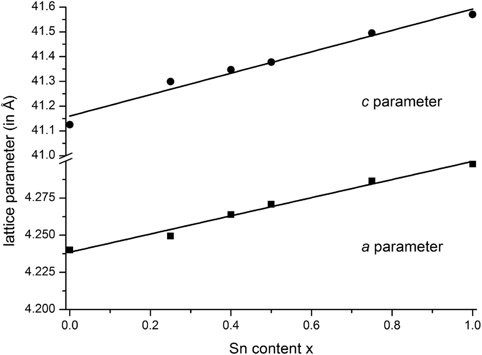
Samples with the compositions (Ge1−xSnx)Sb2Te4 (x = 0.25, 0.40, 0.50, 0.75) were obtained from stoichiometric melts of the elements. Rietveld refinements prove that they are single-phase and that all members of the solid solution series exhibit a 21R-type structure (space group R![[3 with combining macron]](https://www.rsc.org/images/entities/char_0033_0304.gif) m), they are isostructural to the end members GeSb2Te425 and SnSb2Te4.23 The trend of the lattice parameters is linear according to Vegard's law over the whole region of the solid solution (Fig. 1). The occupancy factors were chosen according to the results of the single-crystal structure analysis based on resonant scattering data (see below). The occupancy of Sb on each cation's Wyckoff position was fixed to the value of Ge0.6Sn0.4Sb2Te4 and the difference to full occupancy was filled with Ge and Sn according to their site preference ratio from the resonant single crystal refinement. With increasing Sn content, the bond lengths between cation and anion positions slightly increase according to the Rietveld refinement results; however, the standard deviations are rather large (cf. Fig. S1 in the ESI†). Yet, this reflects the larger ionic radius of Sn in comparison to Ge. Fig. 2 shows the result of the Rietveld refinement for Ge0.5Sn0.5Sb2Te4, the other plots are given in the ESI (Fig. S2–S4†). Crystallographic data are summarized in Table 1, the refined parameters are given in Table 2.
m), they are isostructural to the end members GeSb2Te425 and SnSb2Te4.23 The trend of the lattice parameters is linear according to Vegard's law over the whole region of the solid solution (Fig. 1). The occupancy factors were chosen according to the results of the single-crystal structure analysis based on resonant scattering data (see below). The occupancy of Sb on each cation's Wyckoff position was fixed to the value of Ge0.6Sn0.4Sb2Te4 and the difference to full occupancy was filled with Ge and Sn according to their site preference ratio from the resonant single crystal refinement. With increasing Sn content, the bond lengths between cation and anion positions slightly increase according to the Rietveld refinement results; however, the standard deviations are rather large (cf. Fig. S1 in the ESI†). Yet, this reflects the larger ionic radius of Sn in comparison to Ge. Fig. 2 shows the result of the Rietveld refinement for Ge0.5Sn0.5Sb2Te4, the other plots are given in the ESI (Fig. S2–S4†). Crystallographic data are summarized in Table 1, the refined parameters are given in Table 2.
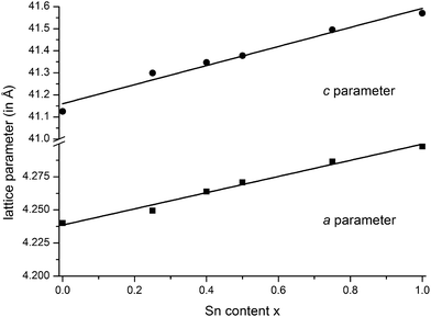 |
| | Fig. 1 Vegard's plot of compounds in the series (Ge1−xSnx)Sb2Te4 (x = 0–1); c parameter (top) and a parameter (bottom); values for GeSb2Te425 and SnSb2Te423 taken from literature. | |
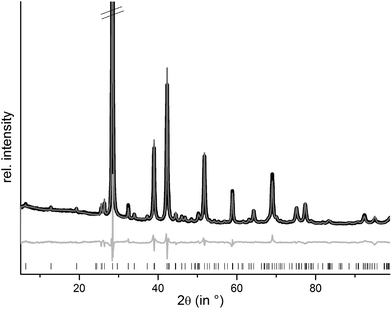 |
| | Fig. 2 Rietveld refinement of 21R-Ge0.5Sn0.5Sb2Te4 (the strongest reflection is cut off); vertical lines indicate calculated reflection positions, experimental (black) and calculated pattern (gray) and difference plot (below) are shown. | |
Table 1 Results from the Rietveld refinements for (Ge1−xSnx)Sb2Te4 compounds with x = 0.25, 0.4, 0.5, 0.75
| Compound |
Ge0.75Sn0.25Sb2Te4 |
Ge0.6Sn0.4Sb2Te4 |
Ge0.5Sn0.5Sb2Te4 |
Ge0.25Sn0.75Sb2Te4 |
| Formula mass (in g mol−1) |
838.06 |
844.97 |
849.58 |
861.11 |
|
F(000) |
1039.5 |
1048 |
1053 |
1066.5 |
| Crystal system/space group |
Trigonal/Rm (no. 166) |
|
Z
|
3 |
| Cell parameters (in Å) |
a = 4.24950(12) |
a = 4.26384(14) |
a = 4.27072(13) |
a = 4.28656(14) |
|
c = 41.299(3) |
c = 41.346(3) |
c = 41.376(3) |
c = 41.495(4) |
| Cell volume (in Å3) |
645.87 (6) |
650.973(7) |
653.66(6) |
660.30(7) |
| X-ray density (in g cm−3) |
6.46 |
6.47 |
6.48 |
6.50 |
| Absorption coefficient (in mm−1) |
162.24 |
163.77 |
164.97 |
167.88 |
| Wavelength (in Å) |
Cu Kα1 (λ = 1.540596 Å) |
| 2θ range (in °) |
5 ≤ 2θ ≤ 99 |
| Profile function |
Fundamental parameters (direct convolution approach) |
| Restraints |
6 |
| Reflections |
115 |
117 |
117 |
119 |
| Parameters/thereof background |
37/18 |
37/18 |
37/18 |
37/18 |
|
R
p/Rwp |
0.0235/0.0349 |
0.0234/0.0340 |
0.0238/0.0342 |
0.0246/0.0369 |
|
R
Bragg
|
0.0350 |
0.0331 |
0.0333 |
0.0332 |
| GooF |
1.326 |
1.436 |
1.451 |
1.567 |
Table 2 Wyckoff positions, atom coordinates, occupancy factors (cf. text: according to nominal composition, not refined) and isotropic displacement parameters Biso (in Å3) for (Ge1−xSnx)Sb2Te4 compounds with x = 0.25, 0.4, 0.5, 0.75
| Atom |
Formula |
Position |
Wyckoff position |
x y z
|
Occupancy |
B
iso
|
| Ge/Sn/Sb |
Ge0.75Sn0.25Sb2Te4 |
C1 |
3a |
0 0 0 |
0.4065/0.1355/0.458 |
1.56(13) |
| Ge0.6Sn0.4Sb2Te4 |
0 0 0 |
0.378/0.1634/0.458 |
1.33(13) |
| Ge0.5Sn0.5Sb2Te4 |
0 0 0 |
0.271/0.271/0.458 |
1.10(9) |
| Ge0.25Sn0.75Sb2Te4 |
0 0 0 |
0.1355/0.4065/0.458 |
1.90(14) |
| Ge/Sn/Sb |
Ge0.75Sn0.25Sb2Te4 |
C2 |
6c |
0 0 0.42746(16) |
0.1718/0.0572/0.771 |
1.56(13) |
| Ge0.6Sn0.4Sb2Te4 |
0 0 0.42740(16) |
0.1107/0.1183/0.771 |
1.34(13) |
| Ge0.5Sn0.5Sb2Te4 |
0 0 0.42725(14) |
0.1145/0.1145/0.771 |
1.10(9) |
| Ge0.25Sn0.75Sb2Te4 |
0 0 0.4277(2) |
0.0572/0.1718/0.771 |
1.90(14) |
| Te |
Ge0.75Sn0.25Sb2Te4 |
A1 |
6c |
0 0 0.13205(15) |
1 |
1.61(11) |
| Ge0.6Sn0.4Sb2Te4 |
0 0 0.13208(15) |
1 |
1.21(11) |
| Ge0.5Sn0.5Sb2Te4 |
0 0 0.13251(14) |
1 |
1.58(12) |
| Ge0.25Sn0.75Sb2Te4 |
0 0 0.1324(2) |
1 |
1.55(12) |
| Te |
Ge0.75Sn0.25Sb2Te4 |
A2 |
6c |
0 0 0.2900(2) |
1 |
1.61(11) |
| Ge0.6Sn0.4Sb2Te4 |
0 0 0.2904(2) |
1 |
1.21(11) |
| Ge0.5Sn0.5Sb2Te4 |
0 0 0.28993(18) |
1 |
1.58(12) |
| Ge0.25Sn0.75Sb2Te4 |
0 0 0.2898(3) |
1 |
1.55(12) |
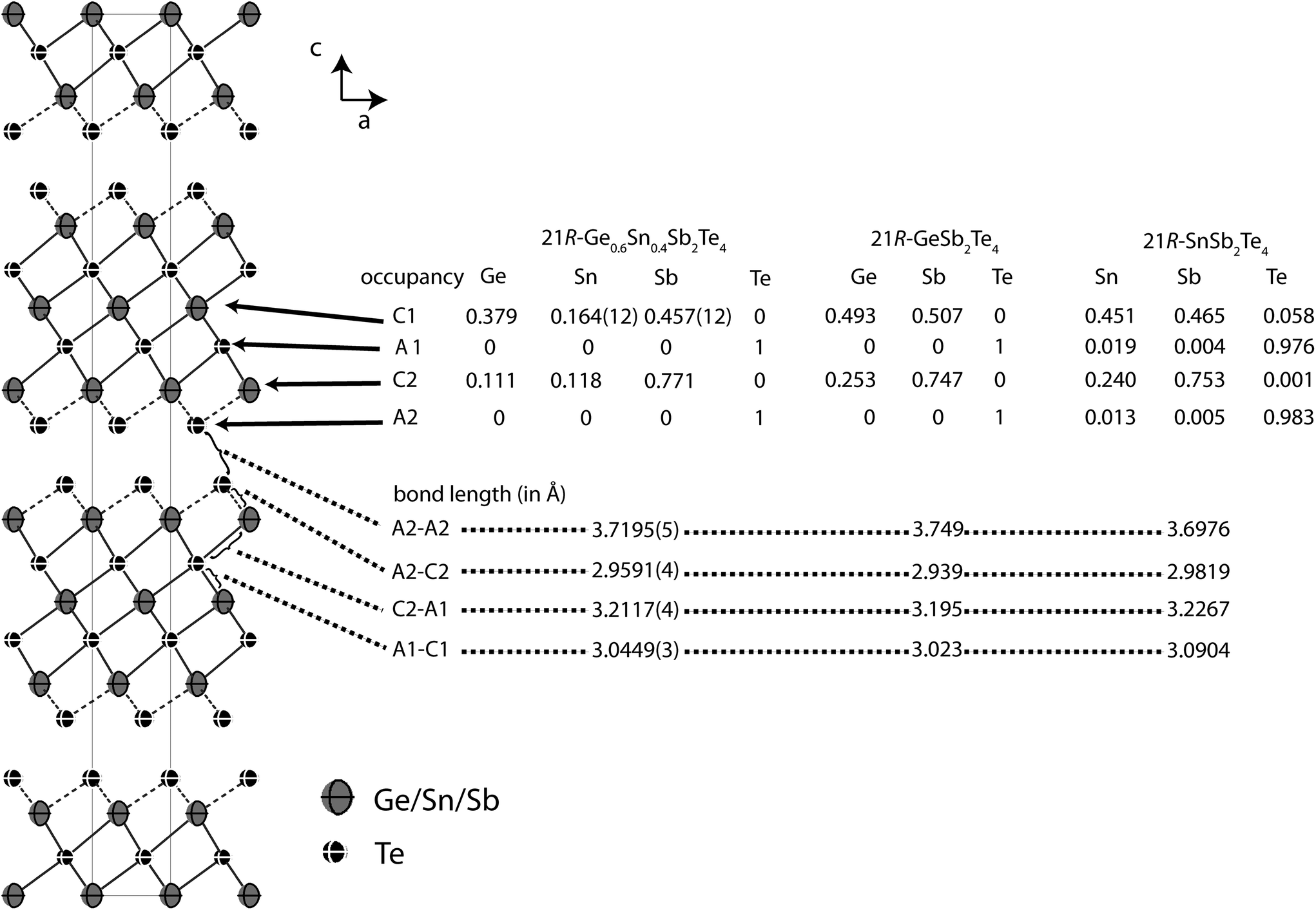
In order to precisely determine the element distribution, a single crystal for resonant diffraction experiments was grown by chemical transport (cf. Experimental section). Energy-dispersive X-ray spectroscopy (EDX) yields a composition of Ge9.5(5)Sn6.0(5)Sb28.7(3)Te55.8(4) (averaged from 3 point analyses). Taking into account normal valence states, this corresponds to the formula Ge0.6Sn0.4Sb2Te4 (calculated atom%: Ge8.6Sn5.7Sb28.6Te57.1). This compound forms a 21R In3Te4-type structure with distorted rocksalt-type slabs as described above, which is depicted in Fig. 3.25–29 The three slabs per unit cell are separated by van der Waals gaps with Te–Te distances (between the atoms A2, cf.Table 4 and Fig. 3) of 3.720 Å which indicate a partially covalent interaction (sum of van der Waals radii: 4.42 Å).30 This is comparable to the corresponding Te–Te distances in 21R-type phases like GeSb2Te4,25 SnSb2Te423 or PbSb2Te4.31 Among all these phases, these distances do not differ more than about 2%. The bond lengths in the distorted 3 + 3 coordination of the cations (C2) next to the van der Waals gap are 2.959 Å towards the gap (C2–A2) and 3.2117 Å towards the center of the slabs (C2–A1), respectively (cf. Fig. 3); the bond angles are A2–C2–A2: 92.19°; A1–C2–A1: 83.18 and A1–C2–A2: 92.15°. The cation-centered octahedra in the middle of the slabs are almost regular with bond lengths of 3.045 Å and angles of 88.88° and 91.12° (A1–C1–A1). While Sn is almost uniformly distributed over both cation positions (occupancy factors 11.8% on position C2 and 16.3% on C1, respectively, cf.Fig. 3), Sb clearly prefers the position near the van der Waals gap (77.1% on position C2). In contrast, the position in the centre of the rocksalt-type slab (C1) shows almost equal amounts of Ge (37.8%) and Sb (45.8%). The same trend can be found in comparable compounds like GeSb2Te4,25 SnSb2Te4,23 PbSb2Te431 and GeBi2Te4.32Tables 3 and 4 summarize the crystal data and give the parameters of the refinement. The atomic coordinates obtained from the single-crystal data and from the corresponding Rietveld refinement are very similar, taking into account their standard deviation, the single-crystal values are of course more precise.
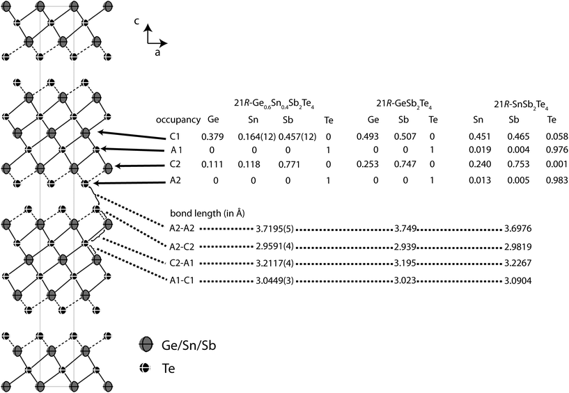 |
| | Fig. 3 Atom distribution (occupancy factors, missing esd’s are a consequence of constraints) for each position and bond length in the refined model of 21R-Ge0.6Sn0.4Sb2Te4 at 293 K (displacement ellipsoids drawn at 99% probability level) compared with GeSb2Te425 and SnSb2Te423 (cation–anion antisite disorder is not significant in SnSb2Te4, the esd’s of the occupancy factors are ∼0.006). | |
Table 3 Crystallographic data on the structure refinement of 21R-Ge0.6Sn0.4Sb2Te4 at 293 K; residual electron density averaged over all datasets
| |
Ge0.6Sn0.4Sb2Te4 |
|
R = ∑|Fo − Fc|/∑|Fo|.
wR = [∑[w(F0 − Fc)2]/∑[w(F0)2]]1/2; w = 1/[σ2(F) + 0.0004 (F02)].
|
| Formula mass (in g mol−1) |
844.97 |
| Cell parameters (in Å) |
a = 4.26384(14), c = 41.346(3) |
| Cell volume (in Å3) |
650.973(7) |
| Crystal system/space group |
Trigonal, Rm (no. 166) |
| X-ray density (in g cm−3) |
6.47 |
|
F(000) |
1048 |
| Formula units (per unit cell) |
3 |
| Crystal size (in mm) |
0.10 × 0.09 × 0.01 |
| Wavelength (in Å) |
0.71073 |
0.56356 |
0.42468 |
0.40681 |
0.38979 |
All datasets |
| Sin(θ)/λ |
0.70 |
0.75 |
0.65 |
0.55 |
0.60 |
|
| Absorption coefficient (in mm−1) |
22.47 |
11.91 |
5.55 |
9.34 |
12.04 |
|
| Measured/independent reflections |
2667/370 |
2112/366 |
5351/790 |
5334/383 |
8716/370 |
|
|
R
int
|
0.0634 |
0.0408 |
0.0310 |
0.0401 |
0.0392 |
|
|
R
σ
|
0.0268 |
0.0374 |
0.0252 |
0.0380 |
0.0277 |
|
| Parameters/restraints |
22/15 |
| Residual electron density (min/max) (in e Å−3) |
−1.91/+3.36 |
|
R
(obs)
|
0.0370 |
0.0533 |
0.0419 |
0.0473 |
0.0366 |
0.0362 |
|
wR
(obs)
|
0.0544 |
0.1082 |
0.0898 |
0.1021 |
0.0754 |
0.0509 |
|
R
(all)
|
0.0424 |
0.0596 |
0.0500 |
0.0536 |
0.0513 |
0.0411 |
|
wR
(all)
|
0.0563 |
0.1092 |
0.0918 |
0.1053 |
0.0811 |
0.0516 |
| GooF(obs) |
1.25 |
2.25 |
1.93 |
2.24 |
1.53 |
1.59 |
| GooF(all) |
1.15 |
2.04 |
1.73 |
2.08 |
1.41 |
1.46 |
Table 4 Structure parameters of 21R-Ge0.6Sn0.4Sb2Te4 at 293 K: atom positions and coordinates, occupancy factors (on each position two parameters were refined and the other is calculated from the difference to full occupancy), equivalent isotropic (ueq in Å2) and anisotropic displacement parameters (uij in Å2; u23 = u13 = 0)
| Atom |
Position |
Wyckoff |
x
|
y
|
z
|
Occupancy |
u
eq
|
u
11 = u22 = 2u12 |
u
33
|
| Ge/Sn/Sb |
C1 |
3a |
0 |
0 |
0 |
Ge 0.379 |
0.02466(17) |
0.0235(2) |
0.0269(3) |
| Sb 0.457(12) |
| Sn 0.164(12) |
| Ge/Sn/Sb |
C2 |
6c |
0 |
0 |
0.426568(11) |
Ge 0.111 |
0.02434(12) |
0.02234(14) |
0.0284(2) |
| Sb 0.771 |
| Sn 0.118 |
| Te |
A1 |
6c |
0 |
0 |
0.132947(8) |
Te 1 |
0.01858(11) |
0.01922(13) |
0.01729(17) |
| Te |
A2 |
6c |
0 |
0 |
0.289989(7) |
Te 1 |
0.01581(10) |
0.01666(13) |
0.01412(17) |
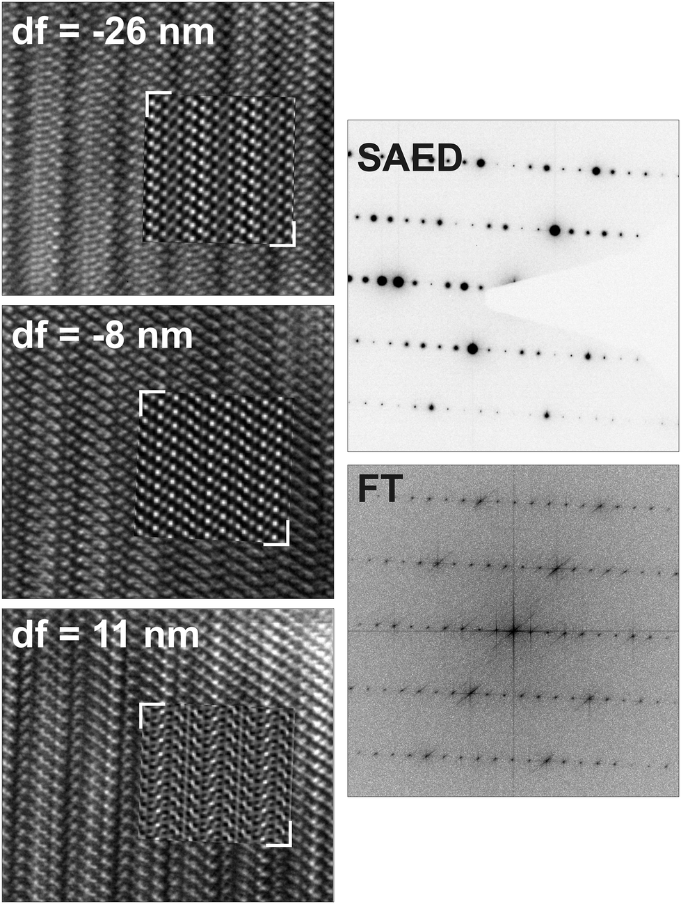
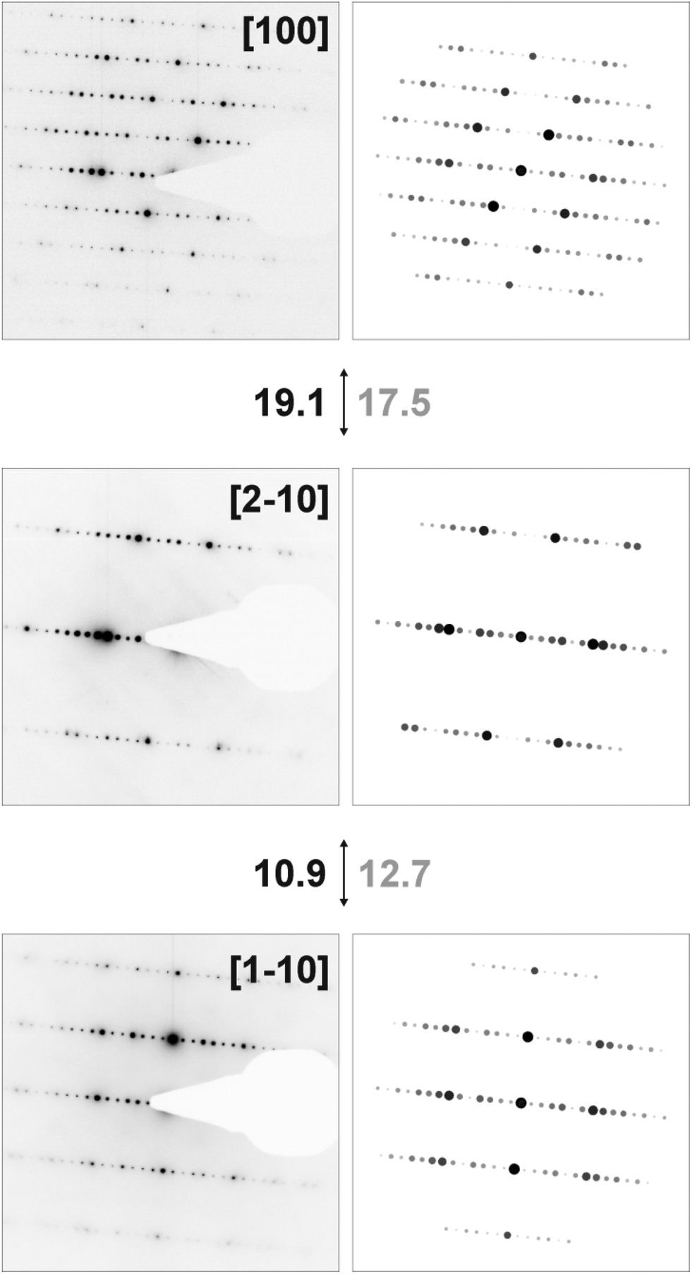
HRTEM images and diffraction patterns of a thinned crystal of Ge0.75Sn0.25Sb2Te4 whose composition was confirmed by TEM-EDX (measured Ge12.2(7)Sn5.5(11)Sb29(2)Te53(2); calculated Ge10.7Sn3.6Sb28.6Te57.1) match well with the simulations (Fig. 4 and 5). The average c parameter from TEM experiments is 41(1) Å in accordance with 41.346(3) Å obtained by X-ray diffraction (Table 1). No phase separation or exsolution was observed; the sample is homogeneous. In the SAED patterns, as well as in the Fourier transform of the HRTEM image, every seventh reflection is strong, which indicates that there are seven layers per rocksalt-type slab corresponding to a trigonal structure (Rm) with a 21R stacking sequence. The variance of the interatomic distances derived from X-ray data is also visible in the HRTEM images; they show sequences of 7 atom layers separated by van der Waals gaps (Fig. 4). This is confirmed by image simulations based on the structure model of Ge0.75Sn0.25Sb2Te4 determined by Rietveld refinement on X-ray powder data. No diffuse intensities along [001]* are visible in the SAED patterns; therefore, no stacking disorder is present.
 |
| | Fig. 4 Fourier filtered HRTEM images (zone axis <100>, different defocus values) with inserted image simulations (thickness 6 unit cells along the viewing direction, Cs = 1.2, spread of defocus 2.14 nm, beam semiconvergence angle of 0.4 mrad) based on the structure model for Ge0.75Sn0.25Sb2Te4 determined by Rietveld refinement on X-ray powder data (left); corresponding Fourier transform (for df = −8 nm) and SAED pattern (right). | |
 |
| | Fig. 5 SAED patterns of Ge0.75Sn0.25Sb2Te4 and corresponding simulations (kinematical intensities) based on the corresponding structure model determined by Rietveld refinement (cf. Tables 1 and 2) with calculated (black) and measured (gray) tilt angles between the zone axes. | |
Mixed crystals (Ge1−xSnx)2Sb2Te5 (x = 0.35, 0.5)
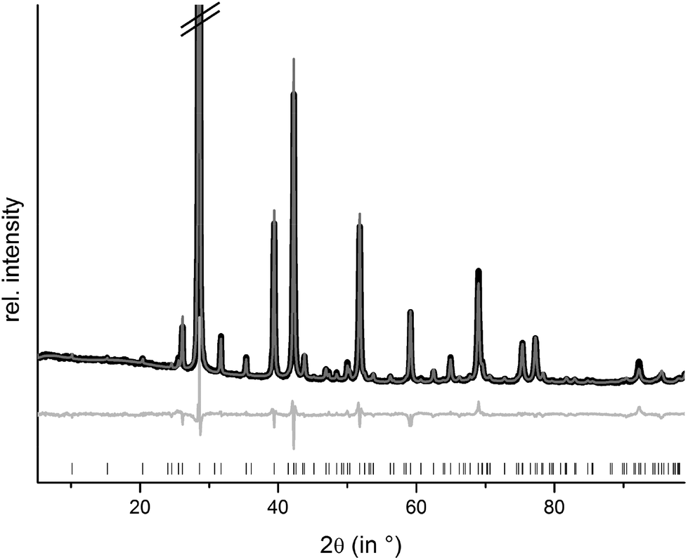
Rietveld refinements confirm that homogeneous samples of (Ge1−xSnxTe)2Sb2Te3 with x = 0.50 and 0.35 could be obtained by melting stoichiometric amounts of the pure elements, quenching in water and subsequently annealing them. The compounds are isostructural to the end member 9P-Ge2Sb2Te5; however, the other end member Sn2Sb2Te5 does not exist. The sample with x = 0.75 contains a small amount of a side phase. This is most likely due to a partial decomposition,8 probably into Ge1−xSnxSb2Te4 and Ge1−xSnxTe. Structure refinements using the Rietveld method were carried out with powder diffraction data of GeSnSb2Te5 and Ge1.3Sn0.7Sb2Te5 (cf. Experimental section). Constraints concerning the sum formula and element distribution were set up in the same way as explained above for (Ge1−xSnx)Sb2Te4. Fig. 6 shows the results of the Rietveld refinement of GeSnSb2Te5, the corresponding data for Ge1.3Sn0.7Sb2Te5 are presented in the ESI (Fig. S5†). Further information about the refinements of the GeSnSb2Te5 and Ge1.3Sn0.7Sb2Te5 powder samples is given in Table 5, the refined atom parameters are listed in Table 6.
 |
| | Fig. 6 Rietveld refinement of 9P-GeSnSb2Te5; (the strongest reflection is cut off); vertical lines indicate calculated reflection positions, experimental (black) and calculated pattern (gray) and difference plot (below) are shown. | |
Table 5 Results from the Rietveld refinements of GeSnSb2Te5 and Ge1.3Sn0.7Sb2Te5
| Sum formula |
Ge1.3Sn0.7Sb2Te5 |
GeSnSb2Te5 |
| Formula mass (in g mol−1) |
1059.01 |
1072.84 |
|
F(000) |
386.6 |
392 |
| Crystal system/space group |
Trigonal/Pm1 (no. 164) |
|
Z
|
1 |
| Cell parameters (in Å) |
a = 4.25792(11) |
a = 4.27486(7) |
|
c = 17.3657(14) |
c = 17.4165(8) |
| Cell volume (in Å3) |
272.66(3) |
275.635(16) |
| X-ray density (in g cm−3) |
6.45 |
6.46 |
| Absorption coefficient (in mm−1) |
158.50 |
161.19 |
| Wavelength (in Å) |
Cu Kα1 (λ = 1.540596 Å) |
| 2θ (in °) |
5 ≤ 2θ ≤ 99 |
| Profile function |
Fundamental parameters (direct convolution approach) |
| Restraints |
6 |
| Reflections |
148 |
148 |
| Parameters/thereof background |
38/18 |
38/18 |
|
R
p/Rwp |
0.0258/0.0375 |
0.0226/0.0340 |
|
R
Bragg
|
0.0212 |
0.0158 |
| GooF |
1.660 |
1.430 |
Table 6 Wyckoff-positions, atom coordinates, occupancy factors (cf. text: according to nominal composition, not refined), isotropic displacement parameters (in Å3) for GeSnSb2Te5 and Ge1.3Sn0.7Sb2Te5 from powder data
| Atom |
Formula |
Position |
Wyckoff position |
x y z
|
Occupancy |
B
iso
|
| Te |
Ge1.3Sn0.7Sb2Te5 GeSnSb2Te5 |
A1 |
1a |
0 0 0 |
1 |
1.56(10) |
| 0 0 0 |
1 |
1.41(8) |
| Ge/Sn/Sb |
Ge1.3Sn0.7Sb2Te5 GeSnSb2Te5 |
C1 |
2d |
2/3 1/3 0.1190(11) |
0.472/0.126/0.402 |
1.70(13) |
| 2/3 1/3 0.1097(9) |
0.299/0.299/0.402 |
2.26(10) |
| Te |
Ge1.3Sn0.7Sb2Te5 GeSnSb2Te5 |
A2 |
1a |
1/3 2/3 0.2065(8) |
1 |
1.56(10) |
| 1/3 2/3 0.2082(6) |
1 |
1.41(8) |
| Ge/Sn/Sb |
Ge1.3Sn0.7Sb2Te5 GeSnSb2Te5 |
C2 |
2c |
0 0 0.3235(6) |
0.178/0.224/0.598 |
1.70(13) |
| 0 0 0.3244(5) |
0.201/0.201/0.598 |
2.26(10) |
| Te |
Ge1.3Sn0.7Sb2Te5 GeSnSb2Te5 |
A3 |
2d |
2/3 1/3 0.4183(8) |
1 |
1.56(10) |
| 2/3 1/3 0.4189(6) |
1 |
1.41(8) |
A single crystal obtained by chemical transport was used for resonant diffraction experiments in order to precisely determine the element distribution. The composition of the single crystal was determined by SEM-EDX. Taking into account electroneutrality, the formula is very close to Ge1.3Sn0.7Sb2Te5 (experiment: Ge15.7(10)Sn8.2(2)Sb21.6(4)Te54.4(14), calculated: Ge14.4Sn7.8Sb22.2Te55.6).
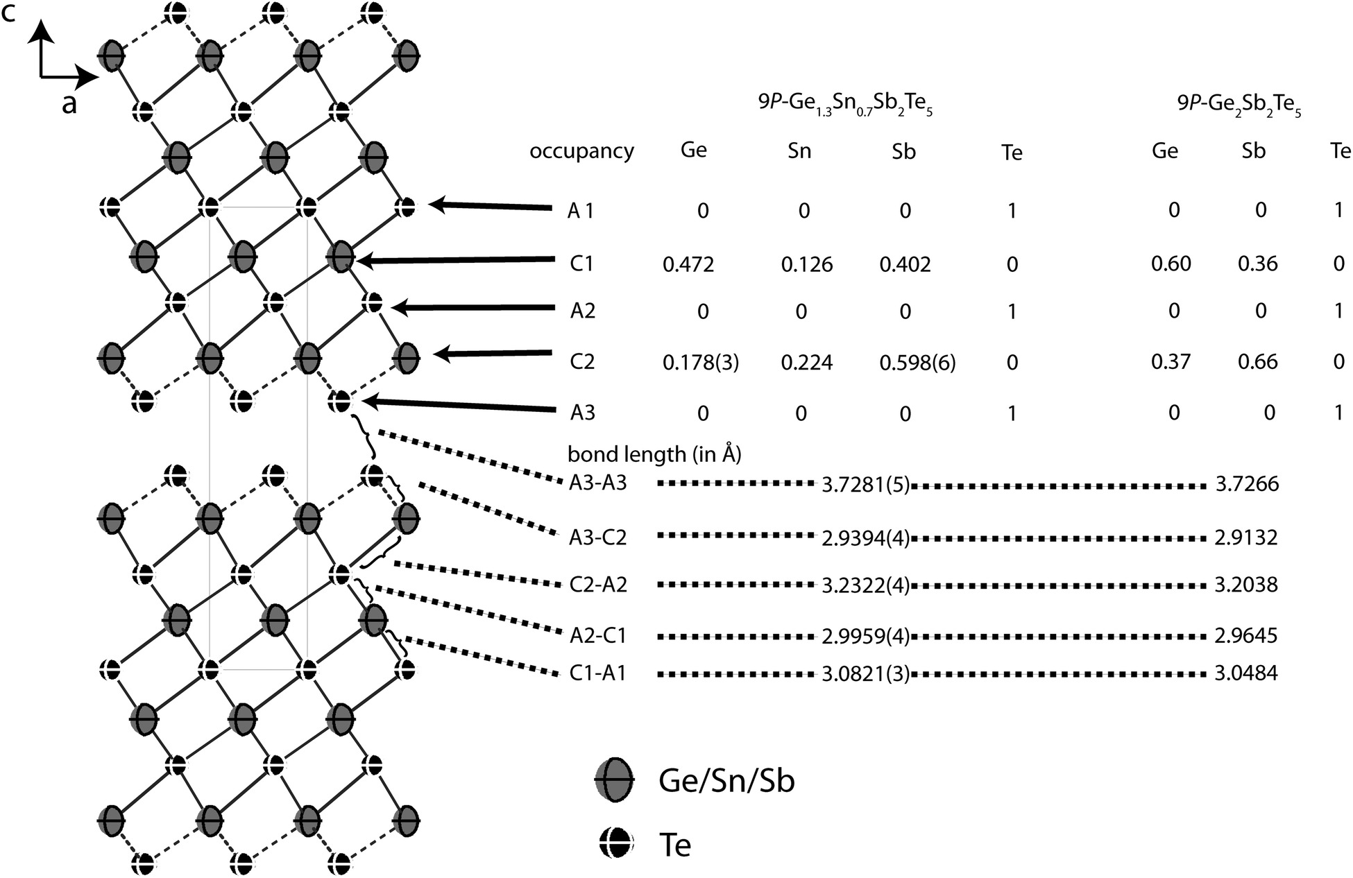
Similar to Ge2Sb2Te5, Ge1.3Sn0.7Sb2Te5 forms the 9P-Pb2Bi2Se5 structure type with 9 alternating anion and cation layers, respectively, per distorted rocksalt-type slab and unit cell. The slabs contain two additional layers compared to 21R-GeSb2Te4 but their arrangement is very similar (cf. Fig. 7). Further information about the structure analysis is given in the Experimental section, Table 7 presents details of the refinement; refined atom parameters are given in Table 8.
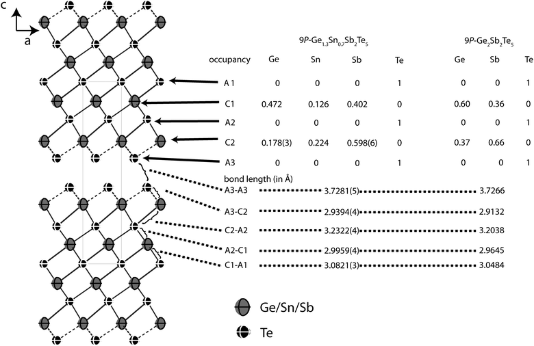 |
| | Fig. 7 Atom distribution (occupancy factors, missing esd's are a consequence of constraints) for each element and bond lengths in the refined model of Ge1.3Sn0.7Sb2Te5 at 293 K (displacement ellipsoids drawn at 99% probability level) compared with Ge2Sb2Te5.24 | |
Table 7 Crystallographic data on the structure refinement of 9P-Ge1.3Sn0.7Sb2Te5 at 293 K; residual electron density averaged over all datasets
| Formula |
Ge1.3Sn0.7Sb2Te5 |
|
R = ∑|Fo − Fc|/∑|Fo|.
wR = [∑[w(F0 − Fc)2]/∑[w(F0)2]]1/2; w = 1/[σ2(F0) + 0.0016(F02)].
|
| Formula mass (in g mol−1) |
1058.96 |
| Cell parameters (in Å) |
a = 4.25793(11), c = 17.3657(14) |
| Cell volume (in Å3) |
270.83(7) |
| Crystal system/space group |
Trigonal, Pm1 (no. 164) |
| X-ray density (in g cm−3) |
6.45 |
|
F(000) |
439 |
|
Z
|
1 |
| Crystal size (in mm) |
0.20 0.09 0.03 |
| Wavelength (in Å) |
0.71073 |
0.56356 |
0.42468 |
0.40681 |
0.38979 |
All datasets |
| Sin(θ)/λ |
0.71 |
0.70 |
0.52 |
0.70 |
0.50 |
|
| Absorption coefficient (in mm−1) |
23.23 |
12.31 |
6.81 |
9.32 |
12.12 |
|
| Measured/independent reflections |
2667/370 |
2112/366 |
5351/790 |
5334/383 |
8440/950 |
|
|
R
int
|
0.0634 |
0.0406 |
0.0310 |
0.0401 |
0.0391 |
|
|
R
σ
|
0.0268 |
0.0374 |
0.0252 |
0.0383 |
0.0254 |
|
| Parameters/restraints |
19/13 |
| Residual electron density (min/max) (in e Å−3) |
−1.95/+2.64 |
|
R
(obs)
|
0.0362 |
0.0516 |
0.0382 |
0.0436 |
0.0350 |
0.0393 |
|
wR
(obs)
|
0.0532 |
0.0771 |
0.0763 |
0.0814 |
0.0700 |
0.0722 |
|
R
(all)
|
0.0416 |
0.0579 |
0.0463 |
0.0498 |
0.0456 |
0.0470 |
|
wR
(all)
|
0.0552 |
0.0786 |
0.0786 |
0.0745 |
0.0745 |
0.0753 |
| GooF(obs) |
1.22 |
1.60 |
1.64 |
1.78 |
1.46 |
1.53 |
| GooF(all) |
1.12 |
1.46 |
1.48 |
1.69 |
1.37 |
1.41 |
Table 8 Structure parameters of 9P-Ge1.3Sn0.7Sb2Te5 at 293 K: atom positions and coordinates, occupancy factors (on each position two parameters were refined and the other is calculated from the difference to full occupancy), equivalent isotropic (ueq in Å2) and anisotropic displacement parameters (uij in Å2; u23 = u13 = 0)
| Atom |
Position |
Wyckoff |
x
|
y
|
z
|
Occupancy |
u
eq
|
u
11 = u22 = 2u12 |
u
33
|
| Te1 |
A1 |
1a |
0 |
0 |
0 |
Te 1 |
0.01699(10) |
0.01752(13) |
0.01593(17) |
| Ge/Sn/Sb2 |
C1 |
2d |
2/3 |
1/3 |
0.10705(3) |
Sb 0.402(6) |
0.02547(13) |
0.02393(16) |
0.0286(2) |
| Ge 0.472(3) |
| Sn 0.126(7) |
| Te3 |
A2 |
2d |
1/3 |
2/3 |
0.205655(18) |
Te 1 |
0.01729(9) |
0.01789(11) |
0.01608(15) |
| Ge/Sn/Sb4 |
C2 |
2c |
0 |
0 |
0.32650(3) |
Sb 0.598(6) |
0.02326(10) |
0.02144(13) |
0.02692(18) |
| Ge 0.178(3) |
| Sn 0.224(7) |
| Te5 |
A3 |
2d |
2/3 |
1/3 |
0.41930(2) |
Te 1 |
0.02015(9) |
0.02072(12) |
0.01900(16) |
Fig. 7 gives an overview of the structure and the element distribution in comparison with Ge2Sb2Te5. The Te atoms at the van der Waals gap (A3) have a distance of 3.728 Å to the next slab, which is slightly larger than for Ge0.6Sn0.4Sb2Te4 (3.720 Å). The bond length alteration in the rocksalt-type slabs is comparable to the 21R-type (Ge1−xSnx)Sb2Te4 phases described above. The coordination sphere of cations near the van der Waals gap (C2) corresponds to distorted octahedrons with shorter bonds (2.939 Å) to the unsaturated Te atoms at the van der Waals gap (A3) and longer ones to the Te atom in the middle of the slab (A2, 3.232) Å; the bond angles indicate pronounced distortion (A3–C2–A3: 92.82°, A3–C2–A2: 92.17°, A2–C2–A2: 82.40°). The C1 octahedrons closer to the center of the slab are more regular with bond lengths of 2.996 and 3.082 Å to the Te atoms A1 and A2, respectively (bond angles: A1–C1–A1: 87.38°, A2–C1–A2: 90.57°; A2–C1–A1: 91.00°). In Ge1.3Sn0.7Sb2Te, all bonds are slightly longer than in Ge0.6Sn0.4Sb2Te4 and Ge2Sb2Te5.24 This is due to the higher Sn content (ionic radii: Sn 0.69 Å, Ge 0.53 Å).30 The larger Sb with its higher oxidation state concentrates on the position C2 near the van der Waals gap (occupancy 59.8%), where Sn (22.4%) is also slightly preferred in comparison to Ge (17.8%). The cation position C1 is occupied by more Ge (47.2%) than Sb (40.2%) and a little Sn (12.6%). The atomic coordinates of Ge1.3Sn0.7Sb2Te5 obtained from single crystal refinement and Rietveld analysis, respectively, differ by up to 10σ. This is probably due to the fact that standard deviations are often underestimated in the Rietveld method.
TEM investigations of the quenched bulk samples of GeSnSb2Te5 corroborate the structure and composition of this quaternary trigonal phase, TEM-EDX measurements yield Ge12.1(2)Sn12.3(2)Sb23.2(5)Te52.5(5) (calculated for GeSnSb2Te5: Ge11.1Sn11.1Sb22.2Te55.5). For a crushed fragment of the ingot with the nominal composition Ge1.3Sn0.7Sb2Te5 used for thermoelectric characterization (see below), EDX yields Ge14.8(2)Sn9.5(2)Sb21.6(5)Te54.0(5) (calculated for Ge1.3Sn0.7Sb2Te5: Ge14.4Sn7.8Sb22.2Te55.5). HRTEM images as well as SAED patterns of the same sample show a d-value of 17 Å which corresponds to the [001]* direction of 9P-Ge2−xSnxSb2Te5. Diffuse streaks along [001]* (cf. Fig. 8) indicate a certain degree of stacking disorder or the presence of rocksalt-type slabs with varying thickness.
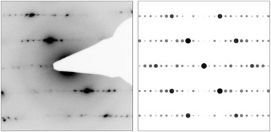 |
| | Fig. 8 Experimental SAED pattern (zone axis <110>, left) of a crystal from a bulk sample of Ge1.3Sn0.7Sb2Te5 and the corresponding calculated one (right) based on the structure model from Ge1.3Sn0.7Sb2Te5. | |
Thermoelectric properties
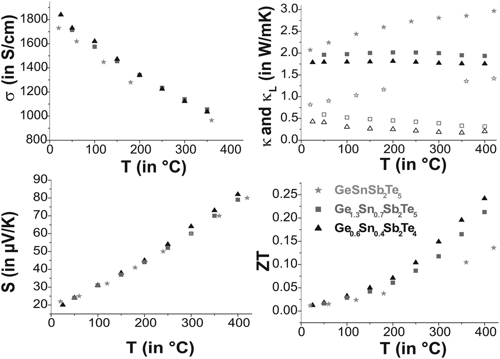
Ge0.6Sn0.4Sb2Te4 and Ge1.3Sn0.7Sb2Te5, for which single-crystal data are available, as well as GeSnSb2Te5 show metallic behavior in their electrical conductivity σ, the absolute values are similar and lie in the range of poor metals (cf. Fig. 9). Compared to water-quenched GeSb2Te4 and Ge2Sb2Te5, which exhibit the crystal structure of the corresponding stable phases, the values of the Sn-containing samples are lower by a factor of 3;33σ of Ge0.6Sn0.4Sb2Te4 is about 50% of that of melt-spun, i.e. rapidly solidified GeSb2Te4 at room temperature and 75% at 430 °C, respectively, while the values of melt-spun Ge2Sb2Te533 are approximately equal to those of quenched Ge1.3Sn0.7Sb2Te5 as reported here. The Seebeck coefficients S of the samples investigated are very similar. The values for Ge1.3Sn0.7Sb2Te5 and GeSnSb2Te5 are in the same range as those of water-quenched Ge2Sb2Te5 and ∼25% lower than those of the melt spun compound between 180 °C and 380 °C.33 This might be due to grain boundaries or anti-site defects in the melt spun sample.
 |
| | Fig. 9 Thermoelectric properties of Ge0.6Sn0.4Sb2Te4, Ge1.3Sn0.7Sb2Te5 and GeSnSb2Te5: electrical conductivity and Seebeck coefficient (left side top to bottom); lattice thermal conductivity (κ bold and κL open faced) and thermoelectric figure of merit (right side top to bottom). | |
The difference in the ZT values is a consequence of the different thermal conductivities κ. These are only 67% (Ge1.3Sn0.7Sb2Te5) and 56% (Ge0.6Sn0.4Sb2Te4), respectively, of those of the unsubstituted samples (3.2 W mK−1 for GeSb2Te4 and 3.0 W mK−1 for Ge2Sb2Te5 at room temperature).34 The phononic part κL of the thermal conductivity (electronic part calculated using L = 2.44 × 10⁻⁸ V2 K−2 which is a typical value for good metals and degenerate semiconductors35) decreases slightly with increasing temperature for Ge0.6Sn0.4Sb2Te4 and Ge1.3Sn0.7Sb2Te5 while it increases for GeSnSb2Te5. Therefore, Sn substitution reduces κ for lower substitution rates (Ge1.3Sn0.7Sb2Te5 and Ge0.6Sn0.4Sb2Te4 compared with Ge2Sb2Te5 and GeSb2Te4), which results in ZT values up to 0.25 higher than those of the unsubstituted samples (ZT up to 0.2).33 Since κ of GeSnSb2Te5 increases with temperature, its ZT value at high temperatures is significantly lower than that of Ge1.3Sn0.7Sb2Te5.
Conclusion
Homogeneous bulk samples of Sn-substituted GST materials have so far been investigated predominantly as thin films, because their performance as PCMs can be enhanced by substituting Sn into the structure.5,6,10 Compounds with a similar composition but a different structure could be obtained as bulk samples by quenching stoichiometric melts of the elements involved. The layered phases of Ge0.6Sn0.4Sb2Te4 and Ge1.3Sn0.7Sb2Te5 show improved thermoelectric properties compared to the stable modifications of GeSb2Te4 and Ge2Sb2Te5 since the thermal conductivity is decreased while the Seebeck coefficient remains nearly unaffected at high temperatures (∼400 °C). The lower thermal conductivity might be due to the introduction of an additional element in the cation substructure that can act as a phonon scattering center. Detailed structural data on the element distribution obtained from single crystals grown by chemical transport reactions show that the cations are not randomly distributed but exhibit clear preferences for certain positions. Ge1−xSnxSb2Te4 and (Ge1−xSnx)2Sb2Te5 form layered phases comparable to those known from the corresponding stable modifications of GST materials. The trend of the element distribution is comparable in the new Sn-containing compounds as well as in unsubstituted GeSb2Te4, Ge2Sb2Te5 and other compounds with the same structure type like SnSb2Te4, PbSb2Te4 and GeBi2Te4.23–25,31,32 The position near the van der Waals gap is preferably occupied by Sb, whereas the position in the center of the distorted rocksalt-type slabs is shared by almost equal amounts of Sb and Ge. Sn shows a slight preference for the position near the van der Waals gap. This element distribution can be explained by the unsaturated coordination of the Te atoms next to the van der Waals gaps, which can be compensated more effectively by Sb3+ than by Ge2+ due to the higher formal charge. The polarizability and covalent bonding character may also play a role and explain why the behavior of Sn is comparable to that of Sb, yet to a lesser extent. The Te–Te distances at the van der Waals gaps are nearly the same for all of the stable 21R-type and 9P-type compounds whereas the cation–anion bond lengths increase slightly with increasing Sn content.
Layered GST materials substituted with Sn open up a field of easily accessible thermoelectrics which can be produced as a bulk material in large amounts. The use of Sn instead of much more expensive Ge may also reduce the cost significantly. As these layered phases are thermodynamically stable, the thermoelectric properties are not influenced by changing nanostructures or by decomposition. The results concerning the element distribution and the distortion of coordination polyhedra may also be valuable as a model for PCMs in order to describe the local environment in amorphous and crystalline thin films of Sn-doped GST materials.
Experimental section
Sample preparation
Bulk samples were prepared by melting stoichiometric mixtures of the elements Ge (99.999%, Aldrich), Sn (99.99%, Alfa Aesar), Sb (99.9999%, Smart Elements) and Te (99.999%, Alfa Aesar) in sealed silica glass ampoules under an argon atmosphere at 950 °C (for 2 h–24 h) and quenching in water. Subsequently, the samples were annealed for about 48 h at temperatures between 450 °C and 590 °C (detailed information can be found in Table S1 in the ESI†). Samples for thermoelectric measurements (ca. 3–4 g) were melted at 950 °C (2 h) in ampoules with a flat bottom, quenched in air, annealed (Ge0.6Sn0.4Sb2Te4: 6 d at 540 °C; Ge1.3Sn0.7Sb2Te5: 2 d at 490 °C; GeSnSb2Te5: 20 h at 550 °C) and subsequently quenched in air. Single crystals of Ge0.6Sn0.4Sb2Te4 and Ge0.75Sn0.25Sb2Te4 were grown by chemical transport reactions in sealed silica glass ampoules under vacuum using ∼20 mg of I2 with temperature gradients from ca. 580 °C to 500 °C for 1 d (composition of the starting material: Ge0.5Sn0.5Sb2Te4 and GeSnSb2Te5, respectively). Ge1.3Sn0.7Sb2Te5 crystals were grown at ∼600 °C (20 h) using the intrinsic gradient of a tube furnace for 20 h from GeSnSb2Te5 as the starting material, adding 20 mg of SbI3 as a transport agent. In all cases, plate-like single crystals could be obtained from the cold end of the ampoule; residual transport agent was removed by washing with acetone.
Electron microscopy and X-ray spectroscopy
The composition of the single crystals used for structure determination was confirmed by energy dispersive X-ray spectroscopy (EDX) on planar crystal faces using a Jeol JSM-6500F scanning electron microscope with an EDX detector (model 7418, Oxford Instruments).
For TEM investigations on Ge1.3Sn0.7Sb2Te5, a finely powdered part of the sample used for thermoelectric measurements was dispersed on a copper grid coated with a holey carbon film. Single crystals of Ge0.75Sn0.25Sb2Te4 (EDX analysis see above) grown by chemical transport were embedded in two-component glue and placed between silicon wafers and glass panels. These “sandwiches” were fixed in brass tubes with an inner diameter 2 mm. Slices of 0.2 mm thickness were cut from the tube and polished to 80–90 μm thickness using SiC coated sandpaper. In the middle of the disks, conical cavities were produced using a dimple grinder (model 650, Gatan) and diamond polishing paste (Electron Microscopy Science) and holes were fabricated using a precision argon ion polishing system (model 691, Gatan). The samples were mounted on a double-tilt holder with maximum tilt angles of ±30°. The measurements were performed on an FEI Titan 80–300 equipped with a field-emission gun operating at 300 kV, a Gatan UltraScan 1000 (2k × 2k) camera and an EDX detector system TOPS 30 (EDAX). The results were evaluated using the Digital Micrograph36 and ES Vision37 software packages. SAED patterns were calculated applying the kinematical approximation and HRTEM images were simulated using the multislice method as implemented in the JEMS38 and EMS program package.39
X-ray powder diffraction
X-ray powder patterns were recorded on a Huber G670 Guinier camera equipped with a fixed imaging plate and integrated read-out system using Cu Kα1 radiation (Ge(111) monochromator, λ = 1.54056 Å). Specimens were prepared by crushing representative parts of the samples and fixing powders on Mylar foils using hair-fixing spray. Lattice parameters were determined by pattern fitting (Rietveld method) using TOPAS ACADEMIC40 with structure models obtained from the single-crystal structure analyses. Shifted Chebychev background functions were used, crystallite strain was described using a Voigt function and preferred orientation was refined with spherical harmonics of the 6th order. All functions were implemented in the TOPAS program suite. Atomic coordinates were set equal for atoms sharing one position and one common isotropic displacement parameter each was used for anions and cations, respectively. Further details of the Rietveld refinements are available from the Fachinformationszentrum Karlsruhe, D-76344 Eggenstein-Leopoldshafen (Germany), on quoting the depository numbers CSD 426668 (Ge0.75Sn0.25Sb2Te4), CSD 426672 (Ge0.5Sn0.5Sb2Te4), CSD 426667 (Ge0.25Sn0.75Sb2Te4) and CSD 426669 (GeSnSb2Te5) as well as the names of the authors and citation of the paper (Fax: +49-7247-808-666; E-mail: E-mail: crysdata@fiz-karlsruhe.de).
Single crystal and synchrotron diffraction methods
Laboratory single crystal datasets were recorded on an IPDS I diffractometer (Stoe & Cie.) with an imaging plate detector using Mo Kα radiation (graphite monochromator, λ = 0.71073 Å). Synchrotron data of the same crystals were collected at beamline ID1141 of the ESRF (Grenoble) on a heavy-duty diffractometer (Huber) with vertical rotation axis equipped with a Frelon2 K CCD detector. The beamline provides a beam tuneable by undulators in the required energy range from 22 keV to 32 keV (0.56 Å to 0.39 Å) near the K absorption edges of Sn (29.195 keV, 0.42468 Å), Sb (30.477 keV, 0.40681 Å), Te (31.818 keV, 0.38979 Å) and far away from the edges (22.00 keV, 0.56357 Å). In order to measure high-angle data, a detector offset was used. The datasets were indexed and integrated using SMART42 and SAINT.43 Laboratory datasets were absorption corrected numerically using XRED44 and XSHAPE;45 synchrotron data consisted of several different datasets, which were combined and absorption corrected semiempirically using SADABS.46 In both cases, the Laue symmetry m was applied. Joint least-squares refinements employing multiple datasets19 were carried out with JANA2006.47 The dispersion correction terms Δf′ and Δf′′ were calculated from X-ray fluorescence spectra (energy-dispersive XFlash detector; Rontec) via the Kramers–Kronig transform48 using the program CHOOCH.49 The refinement aimed at determining the element distribution in the compounds simultaneously for each element on each crystallographic position; full total occupancy was assumed on all atom positions as suggested by the results of previous investigations.22–24 Occupancy factors were constrained in order to fix the sum formula according to the result of the EDX measurements to prevent the overall scale factor from diverging. Elements with occupancy factors close to zero within their standard deviation (or slightly negative) were deleted on the respective positions until only elements with occupancy factors >3σ were present. Atomic coordinates and ADPs of atoms occupying the same site were set as equal. Cell parameters determined from powder samples have been used due to their higher precision. Further details of the single-crystal structure investigation are available from the Fachinformationszentrum Karlsruhe, D-76344 Eggenstein-Leopoldshafen (Germany), on quoting the depository number, CSD 426670 (Ge0.6Sn0.4Sb2Te4) and CSD 42671 (Ge1.3Sn0.7Sb2Te5) as well as the names of the authors and citation of the paper (Fax: +49-7247-808-666; E-mail: E-mail: crysdata@fiz-karlsruhe.de).
Thermoelectric properties
Commercial and in-house-built facilities of the DLR (Cologne) were used to determine the temperature dependence of the electrical and thermal conductivities as well as the Seebeck coefficient from room temperature up to approximately 500 °C under a He atmosphere. Peltier influences on the measurement of the electrical conductivity were reduced by a four-point-probe setup using an AC method (low frequency method using 7 Hz). The electrical resistivity was calculated according to ρ = (1/GF) × R, (GF: correction of cross section and thickness of the sample as well as distance between probe tips). For the determination of the Seebeck coefficient a small temperature gradient across the sample was established while slowly changing the environment temperature in order to obtain Seebeck coefficients for each mean sample temperature. Type-N thermocouples were directly attached to the sample in order to measure both the Seebeck voltage and the temperature.50,51 The thermal conductivity was calculated from the thermal diffusivity (measured using a laser-flash apparatus, Netzsch LFA 427), the heat capacity (determined by differential scanning calorimetry, Netzsch DSC 404), and the density of the samples (measured using a Mohr's balance). The experimental errors were estimated at 5% for the electrical conductivity, 5% for the Seebeck coefficient, and 8% for the thermal conductivity. The data were calculated by averaging between heating and cooling measurements; the values were interpolated to get 50 °C steps in order to calculate ZT and κL.
Acknowledgements
We thank T. Miller for laboratory single-crystal data collections, C. Minke for SEM operation and EDX analyses and W. Schönau for technical support with the thermal conductivity measurements. Special thanks go to Dr Gavin Vaughan and Dr Jonathan Wright for their help during synchrotron data collection and evaluation as well as to Dr Loredana Erra for her support during measurements at ESRF. Preliminary studies by Dr M. N. Schneider are acknowledged. We gratefully acknowledge Prof. Dr W. Schnick's generous support of this work. This investigation was funded by the Deutsche Forschungsgemeinschaft (grant OE530/1-2) and the ESRF (project HS-4363). Part of the project was also financed by the European Union (European Social Fund, NFG “Effiziente Energienutzung: Neue Konzepte und Materialien”).
Notes and references
- M. Wuttig and S. Raoux, Z. Anorg. Allg. Chem., 2012, 638, 2455 CrossRef CAS.
- S. Raoux, Annu. Rev. Mater. Res., 2009, 39, 25 CrossRef CAS.
- T. Siegrist, P. Merkelbach and P. Wuttig, Annu. Rev. Condens. Matter Phys., 2012, 3, 215 CrossRef CAS.
- T. Matsunaga, H. Morita, R. Kojima, N. Yamada, K. Kifune, Y. Kubota, Y. Tabata, J.-J. Kim, M. Kobata, E. Ikenaga and K. Kobayashi, J. Appl. Phys., 2008, 103, 093511 CrossRef.
- K. Wang, D. Wamwangi, S. Ziegler, C. Steimer, M. J. Kang, S. Y. Choi and M. Wuttig, Phys. Status Solidi A, 2004, 201, 3087 CrossRef CAS.
- R. Kojima and N. Yamada, Jpn. J. Appl. Phys., 2001, 40, 5930 CrossRef CAS.
- C. Xu, B. Liu, Z.-T. Song, S.-L. Feng and B. Chen, Chin. Phys. Lett., 2005, 22, 2929 CrossRef CAS.
- W. D. Song, L. P. Shi, X. S. Miao and C. Chong, Appl. Phys. Lett., 2007, 90, 91904 CrossRef.
- J. Xu, F. Rao, Z. Song, M. Xia, C. Peng, Y. Gu, M. Zhu, L. Wu, B. Liu and S. Feng, Electrochem. Solid-State Lett., 2012, 15, H59 CrossRef CAS.
- K. Wang, C. Steimer, D. Wamwangi, S. Ziegler, M. Wuttig, J. Tomforde and W. Bensch, Microsyst. Technol., 2007, 13, 203 CrossRef CAS.
-
D. R. Lide, CRC Handbook of Chemistry and Physics, CRC, New York, 82nd edn, 2001, pp. 9–51 Search PubMed.
- M. N. Schneider, T. Rosenthal, C. Stiewe and O. Oeckler, Z. Kristallogr., 2010, 224, 463 Search PubMed.
- T. Rosenthal, M. N. Schneider, C. Stiewe, M. Döblinger and O. Oeckler, Chem. Mater., 2011, 23, 4349 CrossRef CAS.
- G. J. Snyder and E. S. Toberer, Nat. Mater., 2008, 7, 105 CrossRef CAS PubMed.
- T. Matsunaga, H. Morita, R. Kojima, N. Yamada, K. Kifune, Y. Kubota, Y. Tabata, J.-J. Kim, M. Kobata, E. Ikenaga and K. Kobayashi, J. Appl. Phys., 2008, 103, 093511 CrossRef.
- S. Roux, W. Wojciech and D. Ielmini, Chem. Rev., 2010, 110, 240–267 CrossRef PubMed.
- T. Matsunaga, N. Yamada and Y. Kubota, Acta Crystallogr., Sect. B: Struct. Sci., 2004, 60, 685 CrossRef PubMed.
- O. G. Karpinsky, L. E. Shelimova, M. A. Kretova and J.-P. Fleurial, J. Alloys Compd., 1998, 268, 112 CrossRef CAS.
- S. Welzmiller, P. Urban, F. Fahrnbauer, L. Erra and O. Oeckler, J. Appl. Crystallogr., 2013, 46, 769 CrossRef CAS.
- J. L. Hodeau, V. Favre-Nicolin, S. Bos, H. Renevier, E. Lorenzo and J. F. Berar, Chem. Rev., 2001, 101, 1843 CrossRef CAS PubMed.
- A. K. Cheetham and A. P. Wilkinson, Angew. Chem., Int. Ed., 1992, 31, 1557 CrossRef.
- M. N. Schneider, F. Fahrnbauer, T. Rosenthal, M. Döblinger, C. Stiewe and O. Oeckler, Chem. - Eur. J., 2012, 18, 1209 CrossRef CAS PubMed.
- O. Oeckler, M. N. Schneider, F. Fahrnbauer and G. Vaughan, Solid State Sci., 2011, 13, 1157 CrossRef CAS.
- P. Urban, M. N. Schneider, L. Erra, S. Welzmiller, F. Fahrnbauer and O. Oeckler, CrystEngComm, 2013, 15, 4823 RSC.
- L. E. Shelimova, O. G. Karpinskii, T. E. Svechnikova, I. Y. Nikhezina, E. S. Avilov, M. A. Kretova and V. S. Zemskov, Inorg. Mater., 2008, 44, 371 CrossRef CAS.
- H. W. Shu, S. Jaulmes and J. Flahaut, J. Solid State Chem., 1988, 74, 277 CrossRef CAS.
- A. G. Talybov, Sov. Phys. Crystallogr., 1961, 6, 40 Search PubMed.
- G. Concas, T. M. de Pascale, L. Garbato, F. Ledda, F. Meloni, A. Rucci and M. Serra, J. Phys. Chem. Solids, 1992, 53, 791 CrossRef CAS.
- T. B. Zhukova and A. I. Zaslavskii, Sov. Phys. Crystallogr., 1972, 16, 796 Search PubMed.
- R. D. Shannon, Acta Crystallogr., Sect. A: Cryst. Phys., Diffr., Theor. Gen. Crystallogr., 1976, 32, 751 CrossRef.
- L. E. Shelimova, O. G. Karpinskii, T. E. Svechnikova, E. S. Avilov, M. A. Kretova and V. S. Zemskov, Inorg. Mater., 2004, 40, 1264 CrossRef CAS.
- O. G. Karpinsky, L. E. Shelimova, M. A. Kretova and J.-P. Fleurial, J. Alloys Compd., 1998, 265, 170 CrossRef CAS.
- F. Yan, T. J. Zhu, X. B. Zhao and S. R. Dong, Appl. Phys A: Solid Surf., 2007, 88, 425 CrossRef CAS.
- P. P. Konstantinov, L. E. Shelimova, M. A. Avilov, M. A. Kretova and V. S. Zemskov, Inorg. Mater., 2001, 37, 662 CrossRef CAS.
- G. S. Kumar, G. Prasad and R. O. Pohl, J. Mater. Chem., 1993, 28, 4261 CAS.
-
DigitalMicrograph 3.6.1, Gatan Software, Brisbane, Australia, 2007 Search PubMed.
-
ESVision, 4.0.164, Emispec Systems Inc., Tempe, USA, 1994–2002 Search PubMed.
-
P. Stadelmann, JEMS, version 3.3525U2008, CIME-EPFL, Switzerland, 1999–2008 Search PubMed.
- P. A. Stadelmann, Ultramicroscopy, 1987, 21, 131 CrossRef CAS.
-
A. Coelho, TOPAS Academic, V. 4.1. Coelho Software, Brisbane, 2007 Search PubMed.
-
G. B. M. Vaughan, J. P. Wright, A. Bytchkov, C. Curfs, C. Gundlach, M. Orlova, L. Erra, H. Gleyzolle, T. Buslaps, A. Götz, G. Suchet, S. Petitdemange, M. Rossat, L. Margulies, W. Ludwig, A. Snigirev, I. Snigireva, H. Sørensen, E. M. Lauridsen, U. L. Olsen, J. Oddershede and H. F. Poulsen, Proceedings of the 31st Risø International Symposium on Materials Science: Challenges in materials science and possibilities in 3D and 4D characterization techniques, 2010, vol. 521, p. 457 Search PubMed.
-
J. L. Chambers, K. L. Smith, M. R. Pressprich and Z. Jin, SMART, V.5.625, Bruker AXS, Madison, USA, 1997–2001 Search PubMed.
-
SAINT, V6.01, Bruker AXS, Madison, USA, 1999 Search PubMed.
-
STOE, X-RED 32, Version 1.03, 2002 Search PubMed.
-
STOE, X-SHAPE, Version 1.05, 1999 Search PubMed.
-
SADABS, V2.03, Bruker AXS, Madison, USA, 1999 Search PubMed.
-
V. Petricek, M. Dusek and L. Palatinus, JANA2006 – The CrystallographicComputing System, Institute of Physics, Praha, Czech Republic, 2006 Search PubMed.
- R. de L. Kronig, J. Opt. Soc. Am., 1926, 12, 547 CrossRef.
- G. Evans and R. F. Pettifer, J. Appl. Crystallogr., 2001, 34, 82 CrossRef CAS.
- J. de Boor, C. Stiewe, P. Ziolkowski, T. Dasgupta, G. Karpinski, E. Lenz, F. Edler and E. Müller, J. Electron. Mater., 2013, 42, 1711 CrossRef.
- J. de Boor and E. Müller, Rev. Sci. Instrum., 2013, 84, 065102 CrossRef CAS PubMed.
Footnote |
| † Electronic supplementary information (ESI) available: Additional graph, table and Rietveld plots for Ge0.75Sn0.25Sb2Te4, Ge0.6Sn0.4Sb2Te4, Ge0.25Sn0.75Sb2Te4, Ge1.3Sn0.7Sb2Te5. See DOI: 10.1039/c4dt00336e |
|
| This journal is © The Royal Society of Chemistry 2014 |
Click here to see how this site uses Cookies. View our privacy policy here.  Open Access Article
 This Open Access Article is licensed under a Creative Commons Attribution-Non Commercial 3.0 Unported Licence