
 Open Access Article
 This Open Access Article is licensed under a Creative Commons Attribution-Non Commercial 3.0 Unported Licence
Thermochemical stability, and electronic and dielectric properties of Janus bismuth oxyhalide BiOX (X = Cl, Br, I) monolayers†
Tilak
Das
 *a and
Soumendu
Datta
b
*a and
Soumendu
Datta
b
aUniversità degli Studi Milano-Bicocca, Dipartimento di Scienza dei Materiali, via R. Cozzi, 55, Milano – 20125, Italy. E-mail: tilak.das@unimib.it
bDepartment of Condensed Matter Physics and Material Sciences, Satyendra Nath Bose National Centre for Basic Sciences, JD Block, Sector-III, Salt Lake City, Kolkata – 700 106, India
First published on 7th February 2020
Abstract
Ultrathin monolayers of bismuth oxyhalide materials BiOX (X = Cl, Br, I) grown along 〈001〉 are studied using first-principles density functional theory. Both pristine BiOX and Janus  (X, X′ = Cl, Br, I) monolayers are investigated by analyzing their structural stability using formation enthalpy and phonon density of states. On the other hand, their thermochemical reactivity is understood from their surface energy trends in symmetric and asymmetric terminations. The theoretically measured optical band gaps and fundamental band gaps of these Janus monolayers are compared with their pristine counterparts BiOX and BiOX′ as well as to the known experimental measurements. All of the possible Janus
  monolayers possess structural, electronic and optical properties intermediate to the corresponding properties of the two associated pristine BiOX and BiOX′ monolayers. According to the formation enthalpy, stabilization is equally favorable for all the monolayers, whereas the lowest surface energy is found for BiOCl0.5Br0.5, leading to excellent thermochemical reactivity which is consistent with recent experimental measurements. The frequency dependent dielectric functions are simulated in the density functional perturbation theory limit, and the optical band gaps are estimated from the absorption and reflectance spectra, and are in excellent agreement with the known experimentally measured values. High frequency dielectric constants of these materials with 2D symmetry are estimated from G0W0 calculations including local field and spin–orbit effects. The larger dielectric constants and wider differences in the charge carriers’ effective masses also provide proof that this new class of 2D materials has potential in photo-electrochemical applications. Thus, fabricating Janus monolayers of these oxyhalide compounds would open up a rational design strategy for tailoring their optoelectronic properties, which may offer guidance for the design of highly efficient optoelectronic materials for catalysis, valleytronic, and sensing applications.
1. Introduction
In the past decade of two dimensional (2D) materials such as graphene and transition metal dichalcogenides (TMDs),1–3 bismuth oxyhalides BiOX (X = Cl, Br, I) have attracted significant research attention due to their applications in medicine,4,5 sensing,6 and green energy harvesting via photocatalysis.7–12 During the last decade, bulk BiOX has seemed to be very useful to the scientific community investigating solar energy conversion applications, due to its promising photo-electrochemical efficiency and band gap that is tuneable over a wide range from the ultraviolet to the visible spectrum of solar light.13,14 In recent times, these materials have also been explored experimentally as well as theoretically which are being another new resource of the 2D materials and useful for valleytronics and band gap engineering.15In its bulk phase, BiOX belongs to a tetragonal space group (P4/nmm; No: 129; symmetry group: D4h) where two square sublattices formed by bismuth layers with stacking faults are extended in the ab-plane (in-plane). A so-called ultrathin monolayer is formed with a chemical stoichiometric formulation of [X1−(Bi2O2)2+X1−] and is extended in the in-plane direction. Two consecutive [X1−(Bi2O2)2+X1−] slabs connect with each other via a weak van der Waals (vdW) interaction, with a spacial separation of ∼2–3 Å along the crystallographic 〈001〉 direction, i.e. the out-of-plane direction (see Fig. 1). Thus, this special layer stacking of the bismuth oxyhalide family opens up the further possibility of exfoliation into 2D nanoflakes using bismuth based oxyhalide materials.
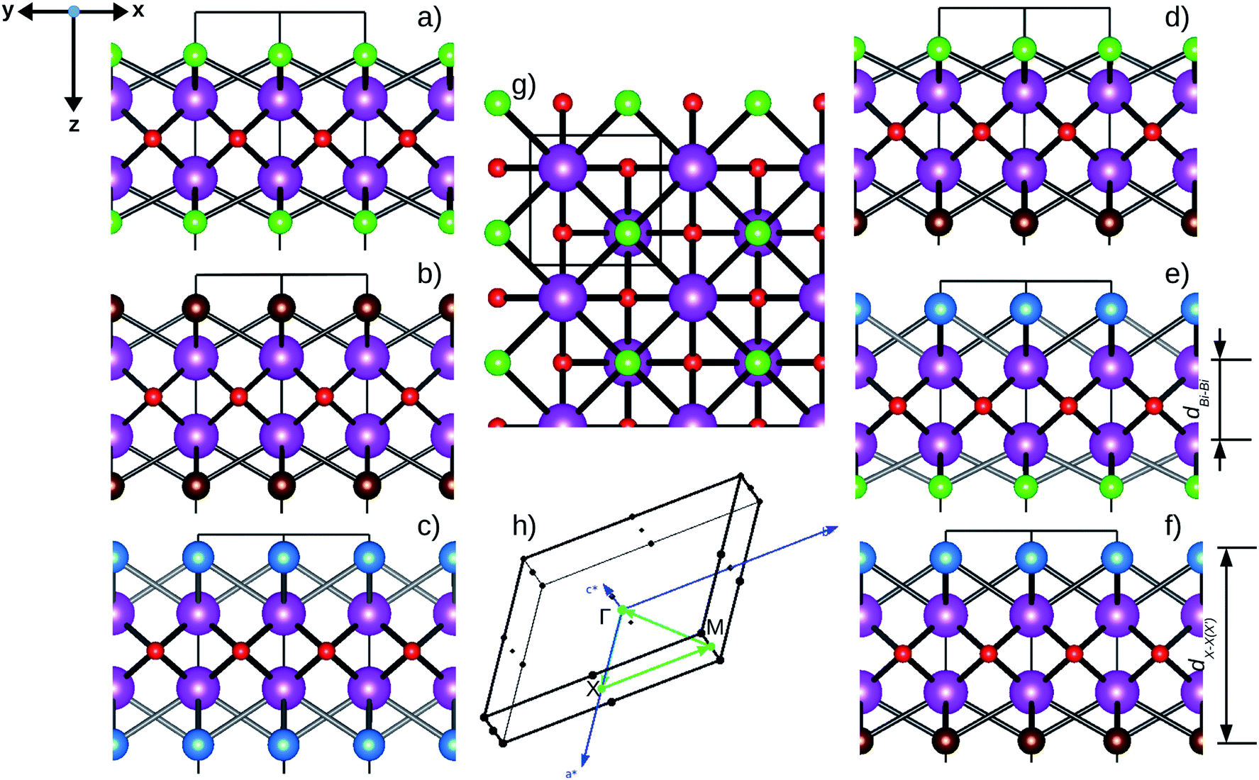 | ||
Fig. 1 Optimized crystal structures of pristine BiOX (left panels a, b, c) and Janus  (right panels d, e, f) monolayers in side view. The conventional tetragonal unit cell is used for all calculations, as marked with the black solid box. The top view is shown only for one case, i.e. the BiOCl monolayer (panel g). The high symmetry k-path is indicated with the green colored solid line in the first Brillouin zone (panel h) for the chosen case of the BiOCl monolayer, and was obtained using the Xcrysden tool. In the structure plots, the large violet colored balls correspond to the Bi atoms, the small red colored balls are the O atoms, and the medium sized green, brown, and blue colored balls are the Cl, Br, and I atoms, respectively, and the plots were obtained with the VESTA crystal structure visualization tool.16 The width of the ML, dX–X(X′), and the inner (Bi2O2)2+ laminar width, dBi–Bi, are marked with double headed arrows. (right panels d, e, f) monolayers in side view. The conventional tetragonal unit cell is used for all calculations, as marked with the black solid box. The top view is shown only for one case, i.e. the BiOCl monolayer (panel g). The high symmetry k-path is indicated with the green colored solid line in the first Brillouin zone (panel h) for the chosen case of the BiOCl monolayer, and was obtained using the Xcrysden tool. In the structure plots, the large violet colored balls correspond to the Bi atoms, the small red colored balls are the O atoms, and the medium sized green, brown, and blue colored balls are the Cl, Br, and I atoms, respectively, and the plots were obtained with the VESTA crystal structure visualization tool.16 The width of the ML, dX–X(X′), and the inner (Bi2O2)2+ laminar width, dBi–Bi, are marked with double headed arrows. | ||
The bulk phases of these BiOX systems are known to be indirect band gap semiconductors, as evident from recent experiments17 and first-principles density functional theory calculations.20,21 The reported electronic band gaps obtained from these calculations for the bulk BiOCl, BiOBr and BiOI systems are 3.37 (3.72), 2.82 (2.93) and 2.00 (2.11) eV, respectively, using plane-wave full-potentials implemented in the LAPW basis Wien2k code and mBJ hybrid calculations22,23 (PAW pseudopotential based HSE06 hybrid functional calculations24,25). These are indeed in reasonable agreement with the available experimentally measured values of 3.4, 2.9 and 1.8 eV, respectively.17 However, the band gaps of crystalline monolayers of BiOX with pristine or Janus morphology are not well discussed in the available experimental or theoretical literature to date. More specifically, a clear discussion of the Kohn–Sham band gap versus the optical band gap obtained from the absorption spectra is still lacking for these 2D materials.
Usually, the 2D morphology of bulk layered semiconducting materials results in efficient photocatalytic properties,26 primarily due to the large specific surface area and efficient separation of the photo-generated electron–hole pairs, and hence longer life-time of the created excitons.18,19 Thus, the 2D structure of these layered oxyhalides, either in the monolayer or few layer morphology, could be useful for standalone photocatalysts for next generation solar energy harvesting. Several recent reports are worth mentioning in this respect, such as the one by Guan et al.12 that enkindles the hope of synthesizing a four layered BiOCl thin film (width ∼2.7 nm) by mechanical exfoliation techniques and subsequent theoretical work27 using hybrid functional calculations within density functional theory (DFT) and predicting a lower binding energy (∼2–8 meV per atom) for monolayer formation. Thus, considering the experimental feasibility of exfoliation of these layered materials, further exploration of the structural as well as photo-induced charge transport properties of 2D thin layers of BiOX materials by detailed computational studies is required.
Recently, a Janus monolayer (ML) of MoSSe was synthesized experimentally by breaking the out-of-plane structural symmetry of the MoS2 layer and replacing the S atomic layer with a Se atomic layer.28 Also, first-principles calculations have predicted that the Janus MoSSe monolayer is a potential water splitting photocatalyst utilizing a wide part of the solar spectrum.29 It is well known that structural symmetry is a key factor in determining the electronic properties in the case of 2D materials. Therefore, breaking the structural symmetry in the pristine monolayer is expected to affect its electronic30,31 and mechanical32 properties, which leads to unusual physical and chemical properties for the Janus morphology.
Nowadays, great efforts have also been made to optimize and improve the optoelectronic properties of bismuth oxyhalide materials in their bulk as well as few layer morphologies by several means33 such as chemical doping,34,35 manipulating vacancy concentrations as well as increasing the defect density,36,37 fabricating solid solutions,38–49 and building heterostructures of BiOX.50,51 However, first-principles calculations investigating the structure, stability and properties of these nanostructured alloys or 2D nanoflakes of BiOX are unknown.52,53 In this respect, an effort to design Janus monolayers from their pristine counterparts considering various halogen combinations would be a smart approach to further engineering the electronic and optical properties of these ultrathin 2D oxyhalide materials.
Thus, in the present study, we have performed a detailed first-principles analysis of the thermochemical and dynamical stabilities, and electronic and dielectric properties of the stoichiometric pristine and Janus monolayers. Taking into account the combination of two halogen species out of the three possibilities (i.e. Cl, Br, I), a total of three Janus  monolayers are feasible, namely BiOCl0.5Br0.5, BiOCl0.5I0.5 and BiOBr0.5I0.5; see Fig. 1 for details. Due to lack of understanding of the chemical and physical properties while moving across from the pristine BiOX to the Janus
  monolayers, we have performed electronic band structure and dielectric function simulations corresponding to their optimized structures. We choose standard ground state DFT calculations based on the PBE-GGA functional including dispersion energy correction at the D3 level and spin–orbit (SO) coupling effects.54,55 The detailed structural stability analysis has been performed in terms of phonon density of states, and formation energy as well as surface energy computation for the symmetric and asymmetric surface terminations with halogen atoms in the respective pristine and Janus monolayers. Also, charge carrier mobilities are discussed in terms of their effective-mass and correlated with their possible role in photocatalytic applications. Finally, optical band gaps are extracted from the Tauc plot over the PBE-D3 + SO functional calculated real and imaginary parts of the dielectric function and correlated with the calculated fundamental band gaps from electronic bands structure and the known experimental optical band gaps. Further analysis of the dielectric constants at the optical frequency limit for materials with 2D symmetry, i.e. monolayers, has been conducted based on the values calculated through single shot GW calculations (G0W0) within 3D periodic boundary conditions using the quasi-electron and quasi-hole approach.56,57 Here, the crystal local field effect (LFE) was included via the random phase approximation (RPA)58 over the ground state wavefunction from the PBE-D3 and PBE-D3 + SO calculations.
2. Computational details
All first-principles calculations have been performed using pseudopotentials and plane-wave basis DFT code with the Vienna Ab initio Simulation Package (VASP).24,25,59 The ion–electron interactions are described via the projector augmented wave (PAW) method. The initial structures of these monolayers have been constructed from the known experimental bulk structures of the respective BiOX systems, which were then fully relaxed (lattice position and stress on the cell volume) using the generalized gradient approximation (GGA) of the exchange-correlation energy functional as formulated by Perdew, Burke and Ernzerhof (PBE)54 and including dispersion correction at the D3 level.55 In addition the effect of spin–orbit coupling is also considered during the structural optimization and calculation of properties.In the valence electronic configuration within the PAW basis choice, we have considered 23 electrons for Bi (5s25p65d106s26p3), 6 electrons for O (2s22p4) and 7 electrons for halogen X (ns2np5) atoms with n = 3, 4 and 5 respectively for Cl, Br and I. For the surface or slab like calculations within the periodic plane-wave approach, a vacuum separation of nearly 20 Å between the slab of material and its neighboring images was chosen.
The convergence of all monolayer structural optimizations was ensured with a 9 × 9 × 1 Monkhorst–Pack k-mesh sampling within the irreducible Brillouin Zone (IBZ). The energy cut-off for the plane-wave expansion was set to 600 eV, while an energy convergence criterion of the order of 10−8 eV for each self-consistency cycle was ensured for reasonable accuracy, with the computed theoretical hydrostatic pressure on the ultrathin monolayers less than 0.1 GPa. More specifically, the structural optimization calculations were performed until the maximal component of force on each atom and stress on the supercell volume of each slab system were close to the known optimum limits as reported previously for other 2D materials including TMDs or MXene and their heterostructures with graphene.3,60–62
For calculating the phonon density of states (DOS) on the pristine and Janus monolayers of bismuth oxyhalides, a minimum 4 × 4 × 1 supercell of the unit cell containing 6 atoms, i.e. a total of 96 atoms, and in-plane parameters ∼15–16 Å, was sufficient for convergence. The dynamical matrices are calculated using the plane-wave VASP code within the finite displacement technique, considering a total of 36 possible displacements in each of the ultrathin film models. Then, for post-processing and estimating force constants and phonon DOS plots, we used the PHONOPY interface63 (more details are given in ESI Section S0†).
The electronic density of states is calculated using the tetrahedron smearing method with energy resolution of 0.01 eV and Gauss broadening of 0.1 eV with a Gamma centered 9 × 9 × 1 k-mesh. The frequency dependent complex dielectric functions, ε(ω), for all the monolayers are calculated with density functional perturbation theory including D3 level dispersion energy correction and spin–orbit coupling effects. A Gaussian broadening of 0.2 eV was applied to the calculated dielectric function, which is comparable to the known experimental broadening limit of 0.1–0.4 eV from ellipsometry measurements of dielectric functions.64,65 The static values of the dielectric constants in the optical frequency limit, ε1(ω = 0), for the monolayers are also computed for the PBE-D3 + SO ground state using the G0W0 method56 as implemented in the VASP code. We find that a Gamma centered k-mesh of dimension 9 × 9 × 1 within the IBZ and four times empty bands were enough for converging the optical transitions and dielectric constants, including local field effects up to the 150 eV plane-wave cut-off via random phase approximation.58 The dielectric constants calculated from the 3D periodic boundary conditions in the PAW methodology are transformed into values for materials with 2D symmetry.66
3. Results and discussion
3.1 Fully optimized geometry of monolayers
In order to gain a better understanding of the qualitative variation of properties from one monolayer to another, either for pristine or Janus models, we have first thoroughly analyzed their optimized crystal structures. Fig. 1 shows the PBE-D3 + SO optimized structures for all six monolayers. The left side panels a, b and c show the pristine monolayers, and the right side panels d, e and f show the Janus models, along with the conventional IBZ in the middle panel h. In the other middle panel, g, the top view of only one pristine monolayer, BiOCl, is shown for clarity.In the case of the pristine monolayers, the (Bi2O2)2+ inner lamina is terminated by the same halogen species [X]1− or [X′]1− on either side of the (001) surface, but in the Janus models the same (Bi2O2)2+ lamina is now terminated by two different halogen atoms [X]1− and [X′]1−. Therefore, to analyze the structural differences between these two classes of monolayers, we have observed the variation of the width of the (Bi2O2)2+ lamina, dBi–Bi, and the total width, dX–X(X′), for each ultrathin monolayer, and their in-plane lattice constants. In the rest of the manuscript text, whenever applicable, we have denoted the stoichiometric Janus monolayers or solid solutions of  using the notation
  (y = 0.5) following the known nomenclature used in the experimental literature.40,41 Our estimated values of the geometric parameters for all six monolayers obtained from both PBE-D3 and PBE-D3 + SO calculations are compared and are given in Table 1.
 monolayers, obtained from PBE-D3 and PBE-D3 + SO calculations. The width of the (Bi2O2)2+ lamina, dBi–Bi, and the total width of the monolayers, dX–X(X′), are tabulated. For each pristine monolayer, computed values of these parameters for the respective bulk systems obtained from a previous first-principles study employing PBE-D3 + SO calculations are provided within the square brackets 21
| Monolayers | a = b (Å) | d Bi–Bi (Å) | d X–X(X′) (Å) | |||
|---|---|---|---|---|---|---|
| PBE-D3 | PBE-D3 + SO | PBE-D3 | PBE-D3 + SO | PBE-D3 | PBE-D3 + SO | |
| BiOCl | 3.88 | 3.88 [3.91] | 2.57 | 2.59 [2.55] | 5.40 | 5.40 [5.20] |
| BiOBr | 3.93 | 3.94 [3.94] | 2.54 | 2.56 [2.53] | 5.77 | 5.78 [5.61] |
| BiOI | 4.02 | 4.03 [4.02] | 2.48 | 2.49 [2.48] | 6.21 | 6.23 [6.13] |
| BiOCl0.5Br0.5 | 3.91 | 3.91 | 2.56 | 2.57 | 5.58 | 5.63 |
| BiOCl0.5I0.5 | 3.95 | 3.95 | 2.53 | 2.54 | 5.81 | 5.83 |
| BiOBr0.5I0.5 | 3.97 | 3.97 | 2.51 | 2.52 | 5.99 | 6.00 |
Similar trends in the changes of the in-plane lattice parameters are seen for bulk phases21 and pristine monolayers.27 The minor impact of structural relaxation on the in-plane lattice parameters of these oxyhalides is similar to other classes of vdW layered oxides – V2O5 or MoO3, as reported earlier.68 The total width of the pristine ML is, however, relatively larger compared to the values for the respective bulk phase. Note that the width of the inner (Bi2O2)2+ lamina for the pristine monolayers decreases with increasing atomic number of the associated halogen species, which is similar to the trend observed for the bulk phases on moving along BiOCl → BiOBr → BiOI. Such a trend is usually expected, as the (Bi2O2)2+ lamina is sandwiched between two layers of heavier halogen atoms. It is also to be noted that the inclusion of the SO coupling effect in the case of the pristine BiOX monolayers slightly affects the width of the inner (Bi2O2)2+ lamina, and the total width, dX–X(X′) is reduced by nearly 0.02 Å (less than 1%).
For each Janus monolayer, it is interesting to note from Table 1 that these three geometric parameters assume almost intermediate values with respect to the corresponding values of the two associated pristine MLs. For example, the in-plane lattice constants and the total width of the Janus BiOBr0.5I0.5 ML are nearly averages of the corresponding values in the pristine BiOBr and BiOI monolayers. A similar trend also exists for the other two Janus MLs. Likewise, the width of the inner (Bi2O2)2+ lamina for each Janus monolayer corresponds to an intermediate value between the respective values for the two associated pristine MLs. It is therefore seen that the qualitative trend in the variation of the lattice parameters for the Janus MLs is the same as that seen for the pristine ML systems if we assign an equivalent atomic number to the halogen species of each Janus model based on the average of the atomic numbers of its two constituent X and X′ halogen species. It should be mentioned here that the lattice constants in a  (y = 0.5) solid solution reported in previous work have been predicted to assume an intermediate value between those for the two pristine BiOX and BiOX′ nanostructures of similar size,53 though the variation of the lattice constant with composition largely deviated from the Vegard’s law type variation. Further, we note from Table 1 that the inclusion of SO coupling for the calculation of lattice parameters in the case of the Janus monolayers does not introduce any drastic changes compared to the trend seen without the SO coupling effect. The SO contribution to the width of the Janus BiOCl0.5Br0.5 monolayer is relatively larger (∼0.05 Å) compared to the rather negligible effect for the other two Janus monolayers (∼0.01 Å). Above all, it is crucial now to better understand their structural and thermodynamical stability because of their simultaneous changes in geometry, and this is discussed in the next section.
3.2 Thermodynamical stability
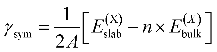
Similar to other 2D materials, the main properties of these newly designed monolayers are essentially governed by their thermodynamical reactivity and stabilities. Thus, the thermodynamical stabilities of these optimized monolayers have been analyzed in the following section by computing their formation enthalpies, as well as surface energies with symmetric and asymmetric termination of two facets. However, note that the impact of thermal expansion has not been explicitly included in the present study. Thus, all energy values are reported at 0 K temperature. Before proceeding to the next subsection, let us discuss the possible structural and dynamical stability of these monolayers based on the PBE-D3 + SO calculations on the fully optimized geometry, as discussed in an earlier section. Indeed, previously reported phonon band dispersion confirms the possibility of dynamically stabilizing these pristine monolayers of BiOX (X = Cl, Br, I).27 Similarly, we have also seen such stability of these pristine phases and report here the results for the BiOCl monolayer in terms of the phonon density of states (see ESI Fig. S1†). In addition, we have also computed the phonon DOS of the Janus models (ESI Section S0†), which shows possible structural stability of the BiOCl0.5Br0.5 and BiOBr0.5I0.5 monolayers, however the Janus BiOCl0.5I0.5 monolayer looks dynamically unstable at the PBE-D3 + SO level. This is probably due to the larger mismatch of the Cl and I atomic radii in these ultrathin films of bismuth oxyhalides.| Eform = Eslab − [n × (μBi + μO) + m × μX + m′ × μX′] | (1) |
 monolayer, obtained from PBE-D3 + SO calculations
| Pristine monolayers | E form (eV f.u.−1) | Janus monolayers | E form (eV f.u.−1) |
|---|---|---|---|
| BiOCl | −3.714 | BiOCl0.5Br0.5 | −3.635 |
| BiOBr | −3.550 | BiOCl0.5I0.5 | −3.451 |
| BiOI | −3.260 | BiOBr0.5I0.5 | −3.386 |
In the first observation from this table, the negative values of the calculated formation energies indicate the feasibility of experimental synthesis of these ultrathin films either in the pristine or Janus configuration. Indeed, the order of magnitude of our calculated formation energies is similar for both types of monolayers (varying within the range −3.3 to −3.8 eV f.u.−1). Therefore, all of them are equally favorable. Among the pristine monolayer systems, it is seen from Table 2 that the formation energies become less negative with increasing halogen atomic number, whereas a mixed trend is found for the Janus systems as expected. Compared with a previous study of first-principles calculations for the pristine cases,27 we note that our calculated results show reasonable agreement and reveal a similar trend. Out of the three pristine systems, the BiOCl monolayer has the lowest formation energy, while the Janus BiOCl0.5Br0.5 monolayer has the lowest formation energy among the three Janus models. Therefore, our results for the formation energy predict that this particular Janus ML will be more likely to be thermodynamically stable with good durability, similar to the pristine BiOCl reported in previous experimental observations,69,70 as well as first-principles theoretical analysis.71 Hence, it is now very crucial to better understand the role of the surface energies in rationalizing the relative thermochemical reactivities, and this is discussed in the next subsection.
 | (2) |
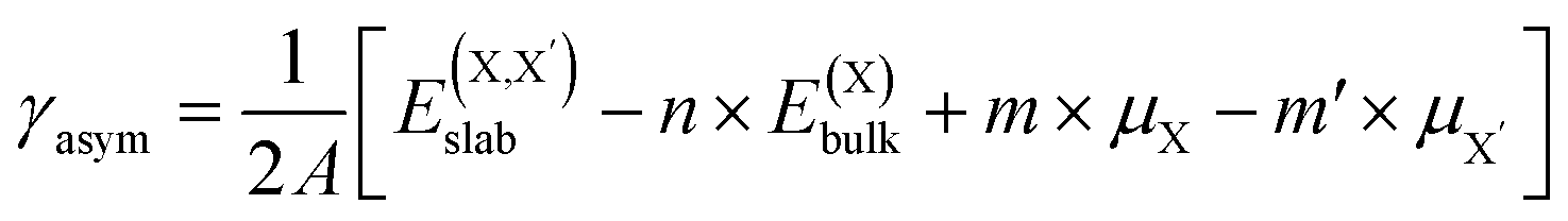 | (3) |
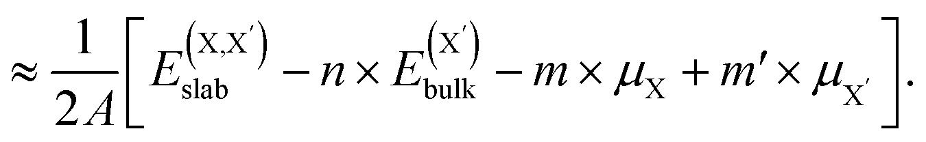 | (4) |
 or
or  and
and  , as obtained from our first-principles calculations. The in-plane surface area A is taken from the fully relaxed geometry of the monolayers. Our calculated values of the surface energies obtained from our PBE-D3 + SO methodology are given in Table 3. It should be noted that the surface energies for the Janus MLs obtained using either eqn (3) or eqn (4) are equivalent, despite the choice of reference bulk pristine unit cell of BiOX or BiOX′.
 monolayers obtained from PBE-D3 + SO calculations
| Pristine monolayers | γ sym (J m−2) | Janus monolayers | γ asym (J m−2) |
|---|---|---|---|
| BiOCl | 0.154 | BiOCl0.5Br0.5 | 0.026 |
| BiOBr | 0.113 | BiOCl0.5I0.5 | 0.417 |
| BiOI | 0.100 | BiOBr0.5I0.5 | 0.277 |
From a first look at Table 3, it is clear that all the values of the calculated surface energies have a similar order of magnitude to those of other recently studied 2D materials based on transition metal chalcogenides, for example MoS2 (ref. 73 and 74), or oxides with 2D facets, like TiO2 (ref. 75). Therefore, these oxyhalide ultrathin films could be expected to have a similar degree of thermodynamical durability and reactivity in their various optoelectronic applications. Among the three pristine monolayers, the order of magnitude of the estimated surface energy varies within the range of 0.1–0.2 J m−2, with the lowest value for the pristine BiOI monolayer. On the other hand, a rather irregular trend in the variation of the surface energies is seen for the Janus monolayers. It is interesting to note that the lowest value appears for the Janus BiOCl0.5Br0.5 monolayer and is nearly 0.03 J m−2, while the largest value corresponds to the Janus BiOCl0.5I0.5 monolayer (0.42 J m−2), and an almost average value is observed for the Janus BiOBr0.5I0.5 monolayer. Thus, the trend in the variation of the surface energies for these Janus monolayers is also interesting, as again their values fall in between the corresponding values for the two associated pristine monolayers, and one may expect a stronger thermodynamical reactivity for the BiOCl0.5I0.5 Janus film. However, it will be harder to synthesize, as it would be difficult to insert and stabilize a larger size I atom in place of a smaller size Cl atom or vice versa. This is consistent with our earlier comment based on the phonon DOS of this particular Janus ultrathin film. On the other hand, the less reactive Janus BiOCl0.5Br0.5 film will be easier to synthesize with the lowest cost of energy due to the similar atomic sizes. In fact, the surface stability of this particular Janus monolayer, BiOCl0.5Br0.5, is five times higher than that of the pristine BiOCl monolayer. Indeed, this is in good agreement with the recently measured surface energy and moderate photocatalytic performance of the crystalline BiOClyBr1−y (y = 0.5) system synthesized via a hydrothermal or solid solution route.40,41 It also is interesting to note that our prediction of the superiority of the Janus BiOCl0.5Br0.5 film is based on the analysis of both the formation enthalpy and the surface energy. Further, according to our estimation, the formation of the Janus BiOBr0.5I0.5 monolayer is feasible due to the moderate energy cost of creation and its thermodynamical reactivity, and this would require further experimental exploration. Thus, it is quite important now to understand the charge carrier dynamics and nature of the band gap obtained from the electronic properties along with the thermodynamic stabilities, and this is discussed in the next section.
3.3 Electronic band structure, effective-mass and density of states
For a preliminary understanding of the electronic properties and their variation in the Janus models, we have analyzed the electronic band structures and effective-masses of the charge carriers at the band-edge extrema along with the density of states around the Fermi level (EF).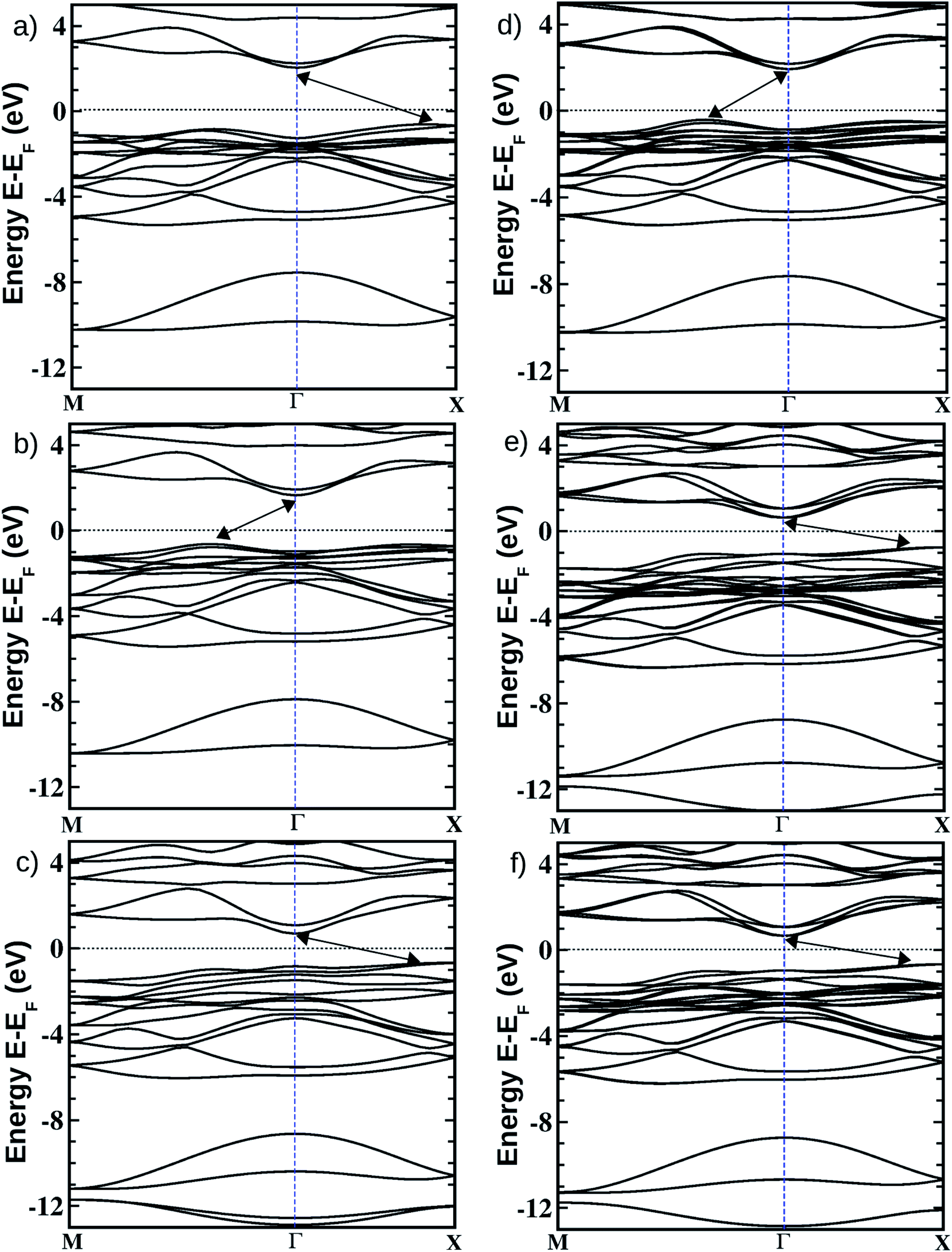 | ||
| Fig. 2 Electronic band structures of the pristine (left side panels a, b, and c respectively for BiOCl, BiOBr, and BiOI) and Janus (right side panels d, e, and f respectively for BiOCl0.5Br0.5, BiOCl0.5I0.5, and BiOBr0.5I0.5) monolayers obtained from PBE-D3 + SO calculations. The zero energy line crossing the y-axis is scaled with respect to the Fermi energy (EF), which is shown with a thin black dotted line. Band-edge extrema are denoted with double headed arrows. | ||
In Table 4, we have provided our PBE-D3 + SO calculated values of the indirect (marked with double headed arrows on the band structure plots) as well as the direct (at Γ-point) band gaps for each of these ultrathin monolayers. Our calculated PBE-D3 + SO indirect band gap values are 2.56 eV, 2.30 eV and 1.35 eV respectively for the pristine BiOCl, BiOBr and BiOI monolayers. Note that the corresponding values for their respective bulk phases were 2.63, 2.11 and 1.46 eV as obtained from previous PBE-D3 + SO calculations.21 Thus, unlike the case of semiconducting quantum dots,76,77 the effect of quantum confinement on the variation of the band gap on going from the bulk phase to the monolayer geometry of these layered oxyhalides is not significant. This has also been observed recently for ultrathin films of other layered oxides like V2O5 and MoO3.68,78 Recently reported fundamental band gaps for the pristine monolayers obtained from DFT calculations using the HSE06 functional are also tabulated in the last column of Table 4. These values are 3.79 (4.80) eV, 3.41 (4.50) eV and 2.3 (3.00) eV, respectively, for the BiOCl, BiOBr and BiOI phases.27,79 Even though the computations are done in the same plane-wave code and the trend of the results is similar in ref. 27 and ref. 79, there is a remarkable difference in their absolute values (off by nearly 1 eV), which is possibly due to different choices for the valence states of the elements, the supercell size in the slab-vacuum model and the plane-wave cut-off energy. However, the magnitudes of these theoretically predicted band gaps appear to be somewhat overestimated by the HSE06 hybrid functional calculations when they are compared with the experimentally reported optical band gap values. Thus, a careful investigation of the optical properties, for example the dielectric function computations and hence the estimation of the optical band gaps, is very crucial for these monolayers, and has not been properly elaborated on in previous studies. Indeed, this has been corroborated in the next section.
| Monolayers | Band gap (eV) | Effective-masses | Previous DFT data (eV) | |||
|---|---|---|---|---|---|---|
| Indirect | Direct | Electron | Hole | GGA | HSE06 | |
| BiOCl | 2.56 | 3.25 | 0.03m0 | 0.13m0 | 2.91 | 3.79, 4.80 |
| BiOBr | 2.30 | 2.58 | 0.02m0 | 0.13m0 | 2.68 | 3.41, 4.50 |
| BiOI | 1.35 | 1.54 | 0.02m0 | 0.23m0 | 1.68 | 2.30, 3.00 |
| BiOCl0.5Br0.5 | 2.34 | 2.79 | 0.03m0 | 0.12m0 | ||
| BiOCl0.5I0.5 | 1.43 | 1.68 | 0.04m0 | 0.21m0 | ||
| BiOBr0.5I0.5 | 1.30 | 1.59 | 0.03m0 | 0.22m0 | ||
On the other hand, for the Janus monolayers it is interesting to note from Table 4 that the estimated band gap for each Janus system lies in between the band gaps of the two associated pristine MLs, for both direct and indirect band gaps. Therefore, there is a relative lowering of the magnitude of the band gap for these Janus  MLs (where atomic number of X′ > atomic number of X) compared to the band gap of one of the constituent pristine monolayers, which will be advantageous for their application in the domains of photocatalysis and electromagnetic field induced optoelectronics.
It is important to mention here that the band gap and the nature of the band-edges play an important role in photocatalytic water splitting.80 In fact, materials with direct band gaps are good absorbers of light photons for creating excitons, whose life-time is quite crucial for redox reactions in photocatalysis or band off-set in optoelectronic device applications. Whereas, an indirect band gap prohibits photon absorption but enhances the life-time of the photo-generated carriers. Thus, a compromise between these two phenomena is a vital feature of these newly designed Janus  models due to their competitive band dispersion. Further, the magnitudes of the direct band gaps are seen to be larger than the magnitudes of the indirect band gaps for the respective monolayers with moderate differences (∼0.1–0.7 eV). Specifically, the dispersions between the direct and indirect transitions in the case of the pristine BiOI as well as the Janus BiOBr0.5I0.5 monolayers are within a small range of 0.1–0.3 eV. Thus, one may expect a small amount of external perturbation such as strain, or a transverse electric field may induce interesting band gap engineering for device applications. An estimation of effective-masses of photo-generated carriers in these monolayers is an alternative way to measure their life-time before recombination, and is discussed in the next subsection.
 are very small within a narrow range of 0.02–0.04m0 on the Γ to X k-path (Γ to M for the pristine BiOBr and Janus BiOCl0.5Br0.5 monolayers) and show very little variation among all the systems. On the other hand, the hole effective-masses
  are comparatively larger and show similar variation within a range of 0.12–0.23m0. The difference in electron and hole effective masses is large (5–10 times). This is advantageous in the suppression of electron–hole recombination for photo-electrochemical applications of these ultrathin monolayers.
The orders of magnitude of the calculated values of  and
and  can be understood from the nature of the band structure at the band-edge extrema, where the second order energy derivative was calculated, which is inversely proportional to the effective masses at the given k-point of the IBZ. The BCB for each monolayer mainly consists of the Bi-6p state which is far away from the Bi nucleus, mostly retains its atom-like properties and possesses large curvature, which gives small values of
  . On the other hand, the TVB consists of the halogen-np state which is relatively closer to its nucleus and is affected more by its nucleus’s attraction. As a result, the curvature of the TVB is less, which results in comparatively large values for
  . It is also seen from Table 4 that
  for the pristine monolayers usually shows an increasing trend with increasing atomic number of the halogen species involved. For the Janus models,
  is large and there is little variation for all three systems due to admixture of the two halogen species involved in the formation of the valence band. It should be pointed out here that the large dispersion of the BCB edge characterizes each of the studied monolayers as an n-type semiconducting material. Hence, visualizing the orbital hybridization with electronic density of states (DOS) is discussed in the next subsection.
 models, the same ordering of admixture of the participating orbitals as seen in the case of the pristine monolayers persists in the formation of their valence and conduction bands, with nearly average contributions from the halogen species corresponding to the X and X′ atoms. More careful analysis of the nature of the band-edges reveals that the TVB originates from the halogen’s np orbital and the BCB originates from the Bi-sp orbital. Due to the different nature of the band-edges, the magnitudes of the effective-masses of electrons and holes are distinctly different. With the TVB being made up of the halogen’s orbitals, it is pushed up with increasing atomic number for the pristine BiOX monolayers, and thereby the band gap decreases (cf.Table 4) simultaneously. In the case of the Janus
  monolayers, the TVB is dominated by the X′-np orbital as the atomic number of X′ is larger than the atomic number of X. Due to hybridization of the X′-np orbitals with the X-np orbitals, the TVB lies grossly in between the TVBs of the pristine BiOX and BiOX′ monolayers. We note that the total width of the valence band is nearly 5 eV for the pristine BiOCl monolayer and increases up to 6 eV as we move from the pristine BiOCl monolayer to the BiOBr and BiOI monolayers, according to our PBE-D3 + SO calculations. Whereas a mixed trend in the valence bandwidth is seen for the Janus monolayers, with calculated values of 5.5–6.2 eV. Overall, the changes in the band gaps for the Janus monolayers happen due to the shifting of the TVB, while the BCB arising from the Bi-sp state remains almost unaffected.
 | ||
| Fig. 3 Calculated total DOS of the monolayers and their corresponding projection onto the Bi, O and halogen atoms, obtained from PBE-D3 + SO calculations. The TDOS, Bi-PDOS and O-PDOS are represented by the shaded black region, and the red and green colored curves, respectively. The Cl-PDOS, Br-PDOS and I-PDOS are represented by the cyan, blue and maroon colored curves, respectively, for both the pristine MLs (left side panels a, b, and c respectively for BiOCl, BiOBr, and BiOI) and Janus MLs (right side panels d, e, and f respectively for BiOCl0.5Br0.5, BiOCl0.5I0.5, and BiOBr0.5I0.5). The zero energy crossing the x-axis is scaled to the Fermi energy (EF). | ||
One of our goals is to elaborate on the technical aspect of optical band gap measurement based on the theoretically measured optical absorption and reflectance spectra obtained from a cheaper first-principles approach. First of all, very high overestimation of the band gap for pristine monolayers of these bismuth oxyhalides does not motivate us to apply the HSE06 hybrid functional. For example, as we have noted, the earlier reported band gaps of the pristine models obtained from the HSE06 functional are 3.79–4.80 eV versus 3.4 eV (experimental) for BiOCl; 3.41–4.50 eV versus 2.9 eV (experimental) for BiOBr; and 2.30–3.00 eV versus 1.8 eV (experimental) for BiOI. Moreover, use of the computationally expensive HSE06 functional would need a further fitting parameter for band gap (scissor operator) without significant impact on the optical transitions. Thus, the hybrid functional HSE06 is not chosen here due to the unexpectedly good band gap results obtained from the PBE-GGA functional (cf.Table 4) which arise from the Bi-sp and O-p hybridization (cf.Fig. 3). However, such strange behavior is well known from the earlier literature on the bismuth based ternary compounds Bi4Ge3O12 and BiVO4 in their bulk phases.81,82 A possible explanation could be the fact that band gap underestimation by Kohn–Sham DFT and incomplete relativistic treatment of Bi electrons lead to this result. More details on the correlation of electronic and optical properties are given in the next section.
3.4 Optical properties simulation
We have calculated the complex frequency dependent dielectric function, ε(ω) within the linear optical properties limit using pseudopotentials and plane-wave based calculations for all monolayers, where ω is comparable to the incident photon energy frequency. The dielectric function is written as ε(ω) = ε1(ω) + iε2(ω). Here, ε1(ω) and ε2(ω) are the real and imaginary parts of the dielectric function, respectively. It must be mentioned in this context that indirect optical transitions are forbidden in our calculations within the linear optical properties limit due to the exclusion of phonons, as discussed earlier for other binary insulators83 and two dimensional low gap semiconductors.84,85 Also, our calculated dielectric function data do not include many-body effects, i.e. excitons and trions.86,87 The calculated average dielectric function is plotted against the incident photon energy for each of these six ultrathin monolayers in Fig. 4. As mentioned earlier, these optical spectra simulations are done within the density functional perturbation theory including dispersion correction at the D3 level, crystal local-field and spin–orbit coupling effects. Details of the real and imaginary parts of the dielectric function with in-plane and out-of-plane polarization are given in ESI Section S3.† In these plots, we have shown the real and imaginary parts of ε(ω) as estimated from PBE-D3 + SO calculations (indigo dashed curves), whereas only the calculated imaginary part, ε2(ω), of the dielectric function obtained from PBE-D3 calculations is given (thick black solid line) in order to visualize the role of spin–orbit effects in optical spectra. | ||
Fig. 4 Calculated frequency dependent real and imaginary parts of the dielectric function, ε1(ω) and ε2(ω), for the pristine BiOX (left side panels a, b, and c for BiOCl, BiOBr, and BiOI respectively) and Janus  monolayers (right side panels d, e, and f for BiOCl0.5Br0.5, BiOCl0.5I0.5, and BiOBr0.5I0.5 respectively) obtained from PBE-D3 + SO (indigo dashed line) and PBE-D3 (black solid line) levels of calculations. The solid tangents in the lower energy parts of the ε2(ω) curves of the PBE-D3 + SO data show the Tauc plots. The vertical dashed lines correspond to the major transitions in jointdensity of states, is the upper bound of the optical band gap within independent particle approximation as visible on ε1(ω). monolayers (right side panels d, e, and f for BiOCl0.5Br0.5, BiOCl0.5I0.5, and BiOBr0.5I0.5 respectively) obtained from PBE-D3 + SO (indigo dashed line) and PBE-D3 (black solid line) levels of calculations. The solid tangents in the lower energy parts of the ε2(ω) curves of the PBE-D3 + SO data show the Tauc plots. The vertical dashed lines correspond to the major transitions in jointdensity of states, is the upper bound of the optical band gap within independent particle approximation as visible on ε1(ω). | ||
Our predicted optical band gaps for these ultrathin monolayers obtained from theoretical optical spectroscopy measurements are tabulated in Table 5. It is seen that the predicted lower bounds of the optical band gaps obtained from the absorption spectra for the pristine monolayers are ∼2.7 eV, 2.1 eV and 1.2 eV respectively for the pristine BiOCl, BiOBr and BiOI monolayers. On the other hand, the predicted upper bounds for these pristine monolayers are ∼3.3 eV, 2.9 eV and 2.1 eV respectively. Note that the reported optical band gaps obtained from recent experimental measurements of UV-vis diffuse reflectance spectra (DRS) and photoluminescence emission spectra of  (y = 1) solid solutions are ∼3.4 eV for BiOClyBr1−y (y = 1), 2.9 eV for BiOBryI1−y (y = 1) and 1.8 eV for BiOIyCl1−y (y = 1) phases, respectively.41 Thus, our predicted optical band gaps obtained using PBE-D3 + SO calculations rather reasonably define the upper and lower bounds for these pristine monolayers, which are ∼3.3–2.7 eV, 2.9–2.1 eV and 2.1–1.2 eV. The effect of spin–orbit coupling has subsequently red shifted the optical band gap by nearly 0.5–0.6 eV, which can be seen from the black solid line plots for ε2(ω).
 , for the pristine as well as the Janus monolayers obtained from different levels of first-principles calculations for 2D slab models are reported. The values in square brackets are obtained from the 3D supercell model with slab-vacuum approach as calculated using the 3D periodic DFT code VASP
| Monolayers | Optical band gap (eV) | Dielectric constant, ε1avg(ω = 0) from 2D Models | |||
|---|---|---|---|---|---|
| Previous know exp.40,41 | Present work PBE-D3 + SO | PBE-D3 | PBE-D3 + SO | PBE-D3 + SO/LFE-RPA | |
| BiOCl | 3.4 | 2.7–3.3 | 5.89 [2.48] | 6.22 [2.55] | 2.42 [2.09] |
| BiOBr | 2.9 | 2.1–2.9 | 7.16 [2.93] | 7.37 [3.03] | 4.72 [2.43] |
| BiOI | 1.8 | 1.2–2.1 | 8.41 [3.55] | 9.50 [3.91] | 7.03 [3.06] |
| BiOCl0.5Br0.5 | 2.77–2.91 | 2.3–3.1 | 6.27 [2.65] | 6.66 [2.77] | 3.51 [2.24] |
| BiOCl0.5I0.5 | 2.10 | 1.9–2.8 | 7.25 [3.01] | 7.81 [3.18] | 5.27 [2.53] |
| BiOBr0.5I0.5 | 2.05 | 1.8–2.3 | 7.57 [3.19] | 8.26 [3.38] | 5.76 [2.67] |
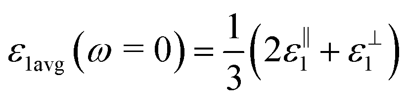
Using the same strategy, our predicted optical band gaps for the Janus  (y = 0.5) monolayers are also quite satisfactory compared to experimental DRS measurements on nanostructured flakes. The predicted optical band gaps for the Janus monolayers as well as the reported experimental values for the corresponding materials are given in Table 5. For example, the optical band gap for crystalline nanostructures of BiOClyBr1−y (y = 0.5) is reported as 2.77–2.91 eV,40,41 whereas our prediction from the absorption spectra in the present study is 2.3–3.1 eV. Likewise, our predicted optical band gaps for the other two Janus monolayers, namely the BiOClyI1−y (y = 0.5) and BiOBryI1−y (y = 0.5) phases are 1.9–2.8 eV and 1.8–2.3 eV, respectively. Note that the experimentally measured optical band gaps for the two crystalline nano-alloy BiOClyI1−y and BiOBryI1−y phases with y = 0.5 are ∼2.10 eV and 2.05 eV, respectively. It is therefore clearly seen that these experimental values for the nanostructured solid solutions or flakes follow a similar trend to that seen in our predictions either from our calculated optical spectra or from our electronic band structure analysis. Once again the band gaps predicted from the absorption spectra in the case of the Janus monolayers have values intermediate to the band gap values of the two associated pristine monolayers. However, we must conclude the section with caution that the optical band gaps (direct band gaps) measured in our theoretically calculated absorption spectra slightly differ from the measured fundamental direct band gaps as seen from the band structure analysis (cf.Table 4). In fact, the computed absorption coefficient in our theoretical calculations is actually proportional to the square of the incident photon energy, therefore a direct band gap is extracted, i.e. the so-called optical band gap, and thus the Tauc tangent must be drawn with care. However, the dielectric constant at the optical frequency limit is one of the crucial parameters for 2D ultrathin films in optoelectronic applications. Finally, at the limit q → 0, using the quasi-particle approach in the G0W0 method including SO effects, the high frequency dielectric constant ε1avg(ω = 0) was estimated, and it is discussed in the next subsection.
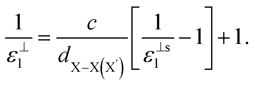
 , for these monolayers calculated at the theoretical levels of PBE-D3, PBE-D3 + SO and PBE-D3 + SO including LFE corrections via RPA (so-called G0W0 method). The in-plane and out-of-plane dielectric constants are denoted with ε‖1 and ε⊥1, respectively. However, note that the computed dielectric constants calculated from periodic code like VASP for 2-dimensional slabs, i.e. monolayers, are limited, and thus one needs to convert the results from pseudo 3-dimensional models into proper 2-dimensional models by eliminating the vacuum effect. From the principle of capacitors connected in series with two dielectric mediums in a slab-vacuum model [pseudo 3D supercell],66,67 the in-plane and out-of-plane parts of the dielectric constants are given respectively by eqn (5) and (6),
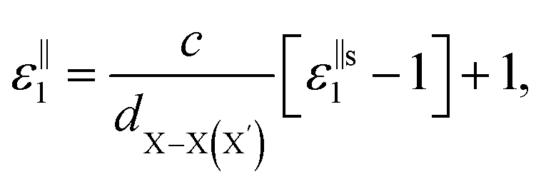 | (5) |
 | (6) |
4 Conclusions and outlook
We have studied the structural and thermochemical stability, and the optoelectronic properties of pristine and Janus monolayers of bismuth oxyhalides, BiOX (X = Cl, Br, I), using the first-principles PBE-D3 + SO level of DFT computations. The calculated values of lattice parameters, band gaps, effective-masses of the charge carriers at the band-edge extrema, and average static dielectric constants for each of the studied Janus monolayers correspond to intermediate values between those observed for the two constituent pristine monolayers BiOX and BiOX′. Structural stability was confirmed from the phonon DOS, i.e. the pristine monolayers are geometrically stable, similar to the known previous literature. On the other hand, two of the Janus monolayers, BiOCl0.5Br0.5 and BiOBr0.5I0.5, are only possibly stable based on their geometry at the PBE-D3 + SO level of theory. According to our surface energy analysis considering both symmetric and asymmetric terminations of the (001) surface, the Janus BiOCl0.5Br0.5 monolayer is energetically more feasible to synthesize. The calculated fundamental band gaps for the studied monolayers are compared with their optical band gaps, considering their potential for solar energy absorption in the UV-vis domain. All these studied monolayers possess an indirect band gap as confirmed by the electronic band structure analysis and a large difference in the effective-masses of electrons and holes (5–10 times). The moderate deviation between the magnitudes of the indirect and direct band gaps for the Janus monolayers is interesting and indicates that a small amount of external perturbation may induce interesting band gap engineering and the possibility of optoelectronic applications. This indeed needs further experimental investigations. The Janus BiOCl0.5Br0.5 monolayer is expected to be an excellent photocatalyst since the optical band gap is in the UV-vis part of the solar spectrum. Our predicted optical band gap for this particular monolayer, 2.3–3.1 eV, is a reasonable match with the known experimental DRS measured optical band gap, 2.77–2.91 eV. The Br atoms in one of the facets of BiOCl0.5Br0.5 have a crucial role in hybridization with Bi, which results in the distinct structural, electronic, and optical properties of this Janus monolayer compared to the pristine BiOCl monolayer. However, the Janus BiOBr0.5I0.5 monolayer would be useful for the same purpose, because it has the largest value of effective-mass difference. We also discovered that the effects of spin–orbit coupling on these monolayers are minor for the structural parameters, but stronger for the dielectric functions. Considering their importance for visible light photocatalytic applications, further experimental investigation using spectroscopic ellipsometry measurements could be useful to validate our predictions about the dielectric constants, ε1(ω = 0), for this new class of two dimensional oxyhalide materials. Also, in future a higher level theoretical investigation using GW-BSE, for example, needs to be performed in order to properly describe excitons and trions in the calculated optical absorption within the UV-vis solar spectrum range.
Conflicts of interest
There are no conflicts to declare.Acknowledgements
S. D. thanks the Department of Science and Technology, India for support through an INSPIRE Faculty Fellowship, Grant No. IFA12-PH-27.References
- K. S. Novoselov, A. K. Geim, S. V. Morozov, D. Jiang, Y. Zhang, S. V. Dubonos, I. V. Grigorieva and A. A. Firsov, Science, 2004, 306, 666 CrossRef CAS PubMed.
- A. K. Geim, Science, 2009, 324, 1530 CrossRef CAS PubMed.
- Q. H. Wang, K. Kalantar-Zadeh, A. Kis, J. N. Coleman and M. S. Strano, Nat. Nanotechnol., 2012, 7, 699 CrossRef CAS PubMed.
- J. Rotmensch, J. L. Whitlock, M. L. Deitz, J. J. Hines, R. C. Reba, E. P. Horwitz and P. V. Harper, Abstr. Pap. Am. Chem. Soc., 1998, 216, U926 Search PubMed.
- G. G. Briand and N. Burford, Chem. Rev., 1999, 99, 2601 CrossRef CAS PubMed.
- C. R. Michel, N. L. L. Contreras and A. H. Martinez-Preciado, Sens. Actuators, B, 2011, 160, 271 CrossRef CAS.
- N. Kijima, K. Matano, M. Saito, T. Oikawa, T. Konishi, H. Yasuda, T. Sato and Y. Yoshimura, Appl. Catal., A, 2001, 206, 237 CrossRef CAS.
- R. Ghosh, S. Maiti and A. Chakraborty, Tetrahedron Lett., 2004, 45, 6775 CrossRef CAS.
- K.-L. Zhang, C.-M. Liu, F.-Q. Huang, C. Zheng and W.-D. Wang, Appl. Catal., B, 2006, 68, 125 CrossRef CAS.
- J. Zhang, F. Shi, J. Lin, D. Chen, J. Gao, Z. Huang, X. Ding and C. Tang, Chem. Mater., 2008, 20, 2937 CrossRef CAS.
- X. Zhang, Z. Ai, F. Jia and L. Zhang, J. Phys. Chem. C, 2008, 112, 747 CrossRef CAS.
- M. Guan, C. Xiao, J. Zhang, S. Fan, R. An, Q. Cheng, J. Xie, M. Zhou, B. Ye and Y. Xie, J. Am. Chem. Soc., 2013, 135, 10411 CrossRef CAS PubMed.
- X. Xiao, C. Liu, R. Hu, X. Zuo, J. Nan, L. Li and L. Wang, J. Mater. Chem., 2012, 22, 22840 RSC.
- D. S. Bhachu, S. J. A. Moniz, S. Sathasivam, D. O. Scanlon, A. Walsh, S. M. Bawaked, M. Mokhtar, A. Y. Obaid, I. P. Parkin, J. Tang and C. J. Carmalt, Chem. Sci., 2016, 7, 4832 RSC.
- D. Deng, K. S. Novoselov, Q. Fu, N. Zheng, Z. Tian and X. Bao, Nat. Nanotechnol., 2016, 11, 218–230 CrossRef CAS PubMed.
- K. Momma and F. Izumi, J. Appl. Crystallogr., 2011, 44, 1272–1276 CrossRef CAS.
- H. An, Y. Du, T. Wang, C. Wang, W. Hao and J. Zhang, Rare Met., 2008, 27, 243 CrossRef CAS.
- S. Haastruo, et al. , 2D Materials, 2018, 5, 042002 CrossRef.
- A. C. Riis-Jensen, M. Pandey and K. S. Thygensen, J. Phys. Chem. C, 2018, 122, 24520–24526 CrossRef CAS.
- A. M. Ganose, M. Cuff, K. T. Butler, A. Walsh and D. O. Scanlon, Chem. Mater., 2016, 28, 1980 CrossRef CAS PubMed.
- S. Dutta, T. Das and S. Datta, Phys. Chem. Chem. Phys., 2018, 20, 103–111 RSC.
- P. Blaha, K. Schwarz, G. K. H. Madsen, D. Kvasnicka and J. Luitz, WIEN2K, An Augmented Plane Wave + Local Orbitals Program for Calculating Crystal Properties, ed. K. Schwarz, Technische Universitiät Wien, Vienna, 2001 Search PubMed.
- F. Tran and P. Blaha, Phys. Rev. Lett., 2009, 102, 226401 CrossRef PubMed.
- G. Kresse and J. Hafner, Phys. Rev. B: Condens. Matter Mater. Phys., 1993, 47, 558–561 CrossRef CAS PubMed; G. Kresse and J. Furthmüller, Comput. Mater. Sci., 1996, 6, 15 CrossRef.
- G. Kresse and D. Joubert, Phys. Rev. B: Condens. Matter Mater. Phys., 1999, 59, 1758–1775 CrossRef CAS.
- A. K. Singh, K. Methew, H. Zhuang and R. G. hennig, J. Phys. Chem. Lett., 2015, 6, 1087 CrossRef CAS PubMed.
- X. Zhang, B. Li, J. Wang, Y. Yuan, Q. Zhang, Z. Gao, L.-M. Liu and L. Chen, Phys. Chem. Chem. Phys., 2014, 16, 25854 RSC.
- A.-Y. Lu, H. Zhu, J. Xiao, C.-P. Chu, Y. Han, M.-H. Chiu, C.-C. Cheng, C.-W. Yang, K.-H. Wei, Y. Yang, Y. Wang, D. Sokaras, D. Nordlund, P. Yang, D. A. Muller, M.-Y. Chou, X. Zhang and L.-J. Li, Nat. Nanotechnol., 2017, 12, 744 CrossRef CAS PubMed.
- X. Ma, X. Wu, H. Wang and Y. Wang, J. Mater. Chem. A, 2018, 6, 2295 RSC.
- F. Li, W. Wei, P. Zhao, B. Huang and Y. Dai, J. Phys. Chem. Lett., 2017, 8, 5959–5965 CrossRef CAS PubMed.
- J. Wang, H. Shu, T. Zhao, P. Liang, N. Wang, D. Cao and X. Chen, Phys. Chem. Chem. Phys., 2018, 20, 18571 RSC.
- Y. Guo, Y. Bai and J. Zhao, Appl. Phys. Lett., 2017, 110, 163102 CrossRef.
- H. Cheng, B. Huang and Y. Dai, Nanoscale, 2014, 6, 2009–2026 RSC.
- G. Jiang, X. Wang, Z. Wei, X. Li, X. Xi, R. Hu, B. Tang, R. Wang, S. Wang, T. Wang and W. Chen, J. Mater. Chem. A, 2013, 1, 2406–2410 RSC.
- L. Zhang, Z.-K. Tang, W.-M. Lau, W.-J. Yin, S.-X. Hu and L.-M. Liu, Phys. Chem. Chem. Phys., 2017, 19, 20968–20973 RSC.
- M. Guan, C. Xiao, J. Zhang, S. Fan, R. An, Q. Cheng, J. Xie, M. Zhou, B. Ye and Y. Xie, J. Am. Chem. Soc., 2013, 135, 10411–10417 CrossRef CAS PubMed.
- Y. Huang, H. Li, M.-S. Balogun, W. Liu, Y. Tong, X. Lu and H. Ji, ACS Appl. Mater. Interfaces, 2014, 6, 22920–22927 CrossRef CAS PubMed.
- T. B. Li, G. Chen, C. Zhou, Z. Y. Shen, R. C. Jin and J. X. Sun, Dalton Trans., 2011, 40, 6751–6758 RSC.
- J. Cao, B. Xu, B. Luo, H. Lin and S. Chen, Catal. Commun., 2011, 13, 63–68 CrossRef CAS.
- H. Gnayem and Y. Sasson, ACS Catal., 2013, 3, 186–191 CrossRef CAS.
- K. Ren, J. Liu, J. Liang, K. Zhang, X. Zheng, H. Luo, Y. Huang, P. Liu and X. Yu, Dalton Trans., 2013, 42, 9706 RSC.
- X. Zhang, L.-W. Wang, C.-Y. Wang, W.-K. Wang, Y.-L. Chen, Y.-X. Huang, W.-W. Li, Y.-J. Feng and H.-Q. Yu, Chem.–Eur. J., 2015, 21, 11872–11877 CrossRef CAS PubMed.
- X. Zhang, C.-Y. Wang, L.-W. Wang, G.-X. Huang, W.-K. Wang and H.-Q. Yu, Sci. Rep., 2016, 6, 22800 CrossRef CAS PubMed.
- H.-Y. Xu, X. Han, Q. Tan, X.-L. He and S.-Y. Qi, Catalysis, 2017, 7, 153 Search PubMed.
- H.-Y. Xu, X. Han, Q. Tan, K.-J. Wu and S.-Y. Qi, Front. Mater. Sci., 2017, 11, 120–129 CrossRef.
- J. Lu, Q. Meng, H. Lv, L. Shui, M. Jin, Z. Zhang, Z. Chen, M. Yuan, X. Wang, J.-M. Liu and G. Zhou, J. Alloys Compd., 2018, 732, 167–177 CrossRef CAS.
- X. Jia, Q. Han, X. Wang and J. Zhu, Photochem. Photobiol., 2018, 94, 942–954 CrossRef CAS PubMed.
- Q. Y. Liu, G. Han, Y. F. Zheng and X. C. Song, Sep. Purif. Technol., 2018, 203, 75–83 CrossRef CAS.
- L. Qi, Y. Yang, P. Zhang, Y. Le, C. Wang and T. Wu, Appl. Surf. Sci., 2019, 467–468, 792–801 CrossRef CAS.
- G. Dai, J. Yu and G. Liu, J. Phys. Chem. C, 2011, 115, 7339–7346 CrossRef CAS.
- L. Kong, Z. Jiang, H. H. Lai, R. J. Nicholls, T. Xiao, M. O. Jones and P. P. Edwards, J. Catal., 2012, 293, 116–125 CrossRef CAS.
- H. Zhang, L. Liu and Z. Zhou, Phys. Chem. Chem. Phys., 2012, 14, 1286–1292 RSC.
- Z.-Y. Zhao, Q.-L. Liu and W.-W. Dai, Sci. Rep., 2016, 6, 31449 CrossRef CAS PubMed.
- J. P. Perdew, K. Burke and M. Ernzerhof, Phys. Rev. Lett., 1996, 77, 3865–3868 CrossRef CAS PubMed.
- S. Grimme, J. Antony, S. Ehrlich and H. Krieg, J. Chem. Phys., 2010, 132, 154104 CrossRef PubMed.
- L. Hedin, Phys. Rev., 1965, 139, A796 CrossRef.
- M. Gajdoš, K. Hummer, G. Kresse, J. Furthmüller and F. Bechstedt, Phys. Rev. B: Condens. Matter Mater. Phys., 2006, 73, 045112 CrossRef.
- S. Baroni and R. Resta, Phys. Rev. B: Condens. Matter Mater. Phys., 1986, 33, 7017 CrossRef CAS PubMed.
- G. Kresse and J. Furthmüller, Phys. Rev. B: Condens. Matter Mater. Phys., 1996, 54, 11169–11186 CrossRef CAS PubMed.
- R. C. Andrew, R. E. Mapasha, A. M. Ukpong and N. Chetty, Phys. Rev. B: Condens. Matter Mater. Phys., 2012, 85, 125428 CrossRef.
- Y. Xie and P. R. C. Kent, Phys. Rev. B: Condens. Matter Mater. Phys., 2013, 87, 235441 CrossRef.
- P. Chakraborty, T. Das, D. Nafday, L. Boeri and T. Saha-Dasgupta, Phys. Rev. B, 2017, 95, 184106 CrossRef.
- A. Togo and I. Tanaka, Scr. Mater., 2015, 108, 1–5 CrossRef CAS.
- N. Vast, L. Reining, V. Olevano, P. Shchattschneider and B. Jouffrey, Phys. Rev. Lett., 2002, 88(3), 037601 CrossRef PubMed.
- L. Lajaunie, F. Boucher, R. Dessapt and P. Moreau, Phys. Rev. B: Condens. Matter Mater. Phys., 2013, 88, 115141 CrossRef.
- A. Laturia, M. L. Van de Put and W. G. Vandenberghe, npj 2D Mater. Appl., 2018, 2(6), 1–6 CAS.
- J. Weng and S.-P. Gao, Phys. Chem. Chem. Phys., 2018, 20, 26453 RSC.
- T. Das, S. Tosoni and G. Pacchioni, Comput. Mater. Sci., 2019, 163, 230–240 CrossRef CAS.
- J. Jiang, K. Zhao, X. Xiao and L. Zhang, J. Am. Chem. Soc., 2012, 134, 4473–4476 CrossRef CAS PubMed.
- K. Zhao, L. Zhang, J. Wang, Q. Li, W. He and J. J. Yin, J. Am. Chem. Soc., 2013, 135, 15750–15753 CrossRef CAS PubMed.
- T. Jing, Y. Dai, X. Ma, W. Wei and B. Huang, Phys. Chem. Chem. Phys., 2016, 18, 7261 RSC.
- X. Tian, T. Wang, L. Fan, Y. Wang, H. Lu and Y. Mu, Appl. Surf. Sci., 2018, 427, 357–362 CrossRef CAS.
- K. Weiss and J. M. Phillips, Phys. Rev. B: Solid State, 1976, 14, 5392 CrossRef CAS.
- Y. Guo, Z. Wang, L. Zhang, X. Shen and F. Liu, Phys. Chem. Chem. Phys., 2016, 18, 14449–14453 RSC.
- N. Roy, Y. Shon and D. Pradhan, ACS Nano, 2013, 7, 2532–2540 CrossRef CAS PubMed.
- S. Datta, M. Kabir, T. Saha-Dasgupta and D. D. Sarma, J. Phys. Chem. C, 2008, 112, 8206–8214 CrossRef CAS.
- S. Datta, M. Kabir and T. Saha-Dasgupta, Phys. Rev. B: Condens. Matter Mater. Phys., 2012, 86, 115307 CrossRef; S. Datta and B. Rahaman, AIP Advances, 2015, 5, 117231 CrossRef.
- F. Li and Z. Chen, Nanoscale, 2013, 5, 5321 RSC.
- M. M. Barhoumi, A. Abboud, L. Debbichi, M. Said, T. Björkman, D. Rocca and S. Lebégue, Beilstein J. Nanotechnol., 2019, 10, 823–832 CrossRef CAS PubMed.
- I. E. Castelli, T. Olsen, S. Datta, D. D. Landis, S. Dahl, K. S. Thygesen and K. W. Jacobsen, Energy Environ. Sci., 2012, 5, 5814–5819 RSC.
- G. E. Jellison Jr, S. Auluck, D. J. Singh and L. A. Boatner, J. Appl. Phys., 2010, 107, 013514 CrossRef.
- M. W. Stoltzfus, P. M. Woodward, R. Seshadri, J.-H. Klepeis and B. Bursten, Inorg. Chem., 2007, 46, 3839–3850 CrossRef CAS PubMed.
- S. Drablia, H. Meradji, S. Ghemid, N. Boukhris, B. Bouhafs and G. Nouet, Mod. Phys. Lett. B, 2009, 23(26), 3065–3079 CrossRef CAS.
- P. Miró, M. Audiffred and T. Heine, Chem. Soc. Rev., 2014, 43, 6537 RSC.
- L. Matthes, O. Pulci and F. Bechstedt, New J. Phys., 2014, 16, 105007 CrossRef.
- K. F. Mak, K. He, C. Lee, G. H. Lee, J. Hone, T. F. Heinz and J. Shan, Nat. Mater., 2013, 12, 207 CrossRef CAS PubMed.
- M. Druppe, T. Deilmann, P. Kruger and M. Rohlfing, Nat. Commun., 2017, 8, 2117 CrossRef PubMed.
- J. K. Cooper, S. Gul, F. M. Toma, L. Chen, Y.-S. Liu, J. Guo, J. W. Ager, J. Yano and I. D. Sharp, J. Phys. Chem. C, 2015, 119, 2969–2974 CrossRef CAS.
- D. Li and W. Y. Ching, Phys. Rev. B: Condens. Matter Mater. Phys., 1996, 54(19), 13616 CrossRef CAS PubMed.
- T. Das, X. Rocquefelte, R. Laskowski, L. Lajaunie, S. Jobic, P. Blaha and K. Schwarz, Chem. Mater., 2017, 29(8), 3380–3386 CrossRef CAS.
- J. C. Tauc, Mater. Res. Bull., 1968, 3, 37–46 CrossRef CAS.
- J. C. Tauc, Optical Properties of Solids, North-Holland, Amsterdam, 1972, p. 372 Search PubMed.
Footnote |
| † Electronic supplementary information (ESI) available. See DOI: 10.1039/c9na00750d |
| This journal is © The Royal Society of Chemistry 2020 |