Polyimide-based microfluidic devices
Stefan
Metz
*,
Raphael
Holzer
and
Philippe
Renaud
Swiss Federal Institute of Technology Lausanne, DMT-IMS, EPFL, CH-1015, Lausanne, Switzerland. E-mail: stefan.metz@epfl.ch
First published on 9th August 2001
Abstract
This paper describes the development of polyimide-based microfluidic devices. A layer transfer and lamination technique is used to fabricate flexible microfluidic channels in various shapes and with a wide range of dimensions. High bond strengths can be achieved by cure cycle adaptation and surface treatment of the polyimide layers prior to bonding. The polyimide microchannels can be combined with metallization layers to fabricate electrodes inside and outside channels. The resulting devices can be used for flexible fluidic and electrical connectors, implantable fluid delivery devices, microelectrodes with embedded fluidic channels, chip-based flow cytometry and for a great variety of other applications in medical, chemical or biological research.
Introduction
Since basic microfluidic devices, such as valves and ink jet printer heads, have made their way to industrial mass production, recent developments in microfluidics have mainly been driven by the ‘lab on a chip’ and ‘μTAS’ vision, where complex microfluidic systems are required for molecular biology, chemistry and medicine. Most microfluidic systems for biology and medicine operate in the low or moderate pressure range. However, when high flow rates are desired, the fluidic device may have to withstand increased internal pressures. Due to the downscaling of surface area, microchannels can also be operated at relatively high pressures. The material from which the channel is fabricated imposes additional constraints, for example, when an insulating material is desired or when distinct surface characteristics are important. Furthermore, it is often necessary to combine additional features, such as electrodes or selective membranes, with the channel structure. Especially for applications in biotechnology and medicine, polymer-based microdevices have gained increased interest due to the low fabrication costs, the well-known micromachining techniques and the wide variety of available materials, such as PDMS,1 PMMA2 or SU-8.3Channels have been micromachined in a great variety of materials and by several well-known methods, including bonding, sacrificial layer techniques and lamination. Bonding techniques require microstructured open channel geometries on one substrate, which are subsequently covered with a second material to form closed channels. Adhesion between the substrates is then established by, for example, anodic bonding4 or fusion bonding.5 By this technique, rigid microchannels have been fabricated in silicon, Pyrex or quartz.
The sacrificial layer method uses a dissolvable material to form the channel geometry. This sacrificial structure is embedded in other materials to form the microchannels and is subsequently removed by solvent dissolution,6 anodically assisted wet etching,7 which is faster than conventional wet etching, or heating.8 Silicon oxide, metals and photoresist have been proposed as sacrificial materials and the technique has been used to manufacture channels in silicon, silicon oxide, metals and several polymers. However, the fabrication method can be quite time consuming, especially for small channel sizes, as the dissolution process is usually diffusion limited.9 This leads to a prolonged exposure of the substrate to the etchant that can result in device destruction due to the harsh chemical environment. A second constraint is imposed by solubility mismatches. For example, easily dissolvable photoresists cannot be used as sacrificial layers for most spin-on polymers, as the solvent inherently present in the liquid polymer precursor will attack the sacrificial layer.
Lamination is probably the most commonly used technique for the fabrication of microfluidic devices in polymers. Open channel structures can be micromachined by laser ablation10 or photolithography11 and subsequently closed by a laminated cover layer. In an additional step, inlet and outlet holes are micromachined for fluidic interconnections. The adhesion and bonding strength at the interface, i.e. substrate and laminated cover layer, is essential for the performance of the microfluidic devices.
For applications in biosciences, polyimides offer advantages over other polymers, such as their excellent chemical and thermal stability, low water uptake and good biocompatibility.12 Furthermore, polyimides are well known from IC manufacturing processes and have already been used to fabricate microfluidic devices.13 Because of the aforementioned advantages, we have chosen polyimides as an IC process compatible material for the fabrication of microfluidic devices.
Different lamination techniques have been proposed to fabricate simple polyimide-based microfluidic devices. Glasgow14 used a polyimide solvent bonding technique where microfluidic devices are fabricated between two wafers. Open channels are patterned on a first wafer, a second wafer is spin-coated with polyimide precursor and the two wafers are put in contact and bonded together in a vacuum oven. The method can suffer from inhibited solvent evaporation during final cure (imidization). As the fabricated channels are located between two wafers, high internal pressures can develop which might create debonding forces. Mangriotis presented a layer transfer technique where a fully cured (imidized) Kapton™ foil is bonded to the open channel structures by using a thin layer of polyimide precursor as adhesive.15 With this method the top layer is not easily structured and only Kapton™ foils with a certain thickness can be used.
This paper presents the development of polyimide-based microfluidic devices where an adapted lamination technique is used to fabricate microchannels in a wide range of geometries and dimensions. We have combined polyimide-based microchannels with metallization layers leading to complex and versatile microfluidic devices. Basic flow characteristics have been investigated and burst pressures tests performed.
Fabrication
An adapted lamination and layer transfer technique was employed to fabricate flexible microfluidic channels by using two different polyimides, a photosensitive type (PI-2732, DuPont) and a non-photosensitive type (PI-2611, DuPont). The first one can be microstructured by photolithography and the second type by dry etching techniques. In the following section we will outline only the fabrication process for the photosensitive polyimide. For the non-photosensitive polyimide the photolithography step can be replaced by dry etching techniques. Polyimide dry etching is best carried out in oxygen plasmas with a silicon oxide etch mask to achieve highly anisotropic etching and avoid mask resputtering.The devices are micromachined on a carrier substrate and resulting structures can be removed from the fabrication support by using a release technique based on anodic metal dissolution of aluminium. If flexible microchannels are not required, the devices can be left on the silicon carrier, which may in turn be used for fluidic interconnection via KOH-etched rear access holes. For the later release of the microstructures, chrome (20 nm), gold (100 nm) and sacrificial aluminium (500 nm) are evaporated on 100 mm Pyrex or silicon substrates. On the aluminium surface, a 5–20 μm thick layer of photosensitive polyimide (PI-2732, DuPont) is applied, photostructured and cured (350 °C) for 1 h under nitrogen in a conventional oven (Fig. 1(a)). Subsequently, a layer of titanium–platinum (50 nm Ti adhesion layer/200 nm Pt metallization layer) is sputtered on the substrate and structured by dry etching using a positive photoresist (3.5 μm S1818, Shipley) as etch mask (Fig. 1(b)). If no metallization layer is required for the actual design, this step can be left out without further modification of the process. A second layer of photosensitive polyimide with a thickness between 5 and 30 μm defines the channel walls and insulates the metallization layer where embedded metallic conductors are desired. For electrodes inside channels or electrical contacts the polyimide is removed (Fig. 1(c)). This layer is spin coated, photostructured and cured under nitrogen for 1 h at 100–150 °C.
 | ||
| Fig. 1 Fabrication steps for polyimide-based microfluidic devices with integrated metallization layer. Metallization step (b) can be skipped if no integrated electrodes are wanted. | ||
For lamination with a polyimide cover layer, the surface is treated with n-methyl-2-pyrrolidone (NMP) (swelling agent), i.e. immersion of the wafer and subsequent spin-drying. As the second layer is not yet completely imidized, there is still polyimide precursor (polyamic acid) present in it. This layer then tends to swell under the influence of a strong solvent, which enables a higher interdiffusion with the layer to be laminated. On a second carrier substrate, a thin Mylar™ foil is made to adhere temporarily through means of surface tension by injecting water between the Mylar™ foil and the wafer. The foil is spin coated with a 5–20 μm thick layer of photosensitive polyimide (Fig. 1(d)). Following a softbake step on a hotplate, the second substrate is flipped over and bonded to the open channel structures of the first wafer by lamination (Fig. 1(e)). The lamination is repeated after removal of the second carrier wafer. After peeling off the Mylar™ foil (Fig. 1(f)), the top layer of polyimide is photostructured and the devices are again cured under nitrogen at 350 °C for 1 h (Fig. 1(g)). For the release (Fig. 1(h)) the wafer with the polyimide electrodes is fixed opposite a Pt counter electrode in a concentrated sodium chloride solution (NaCl–H2O, 1∶5). A positive potential is applied to the wafer with the polyimide devices in the range of several hundred millivolts. During the anodic metal dissolution process16 of aluminium, the gold remains on the substrate due to the difference in the electrochemical potential compared with aluminium and ensures electrical contact until the structures are released. This release is a gentle and smooth process as it can be carried out in a sodium chloride water solution at room temperature. Due to the low water absorption of the polyimide the devices are not damaged during this procedure and no residual aluminium was observed on the dissociated devices. After release, the polyimide structures need to be rinsed and dried. Fluidic interconnection is established by gluing metallic connectors on the channel inlets. For connecting the electrical leads to external circuitry, multi-pole connectors can be reflow-soldered to the contact pads on the polyimide. Combining the devices with the external connectors can be carried out before or after their release from the fabrication support.
Results
Microfluidic channels with a great variety of shapes and dimensions have been fabricated. The flexible channels have heights of 5–20 μm, widths from 30 to 500 μm and lengths of up to 7 cm. We have fabricated multi-channel structures with separated channels, channel junctions and channel intersections. Fig. 2 shows two adjacent channels with 100 μm width and 20 μm internal channel height. No interface is visible between the open channel pre-structures and the laminated top layer, which indicates good channel sealing. Fig. 3 shows the channel inlet/outlet to which metallic tubes are connected with epoxy glue for prototyping (see also Fig. 5). | ||
| Fig. 2 Cross-section of two adjacent channels in polyimide (width 100 μm, height 20 μm). No interface is visible at the laminated junction between the channel pre-structures and the cover layer. | ||
 | ||
| Fig. 3 Fluidic inlet/outlet with a microchannel leading towards it (channel width 200 μm). The inlet is later connected to metallic tubes by epoxy glue (see also Fig. 5). | ||
 | ||
| Fig. 4 Cross-section of a wide channel (width 500 μm, height 20 μm). For an aspect ratio of 25 (width/height) the lamination technology yields open channels without deflection. | ||
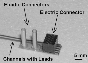 | ||
| Fig. 5 Microprobe combining fluidics with electrodes for electrophysiological stimulation and recording. Electric and fluidic interconnection is established with reflow-soldered, surface-mounted multipole connectors and glued metallic tubes. Devices with up to 4 electrodes and two independent channels have been realized. | ||
The imidization results in shrinkage of the polyimide (30–40%), which decreases the height of the film and degrades the sharpness of the sidewalls. Apart from the decrease in feature size, we have not observed any problems with deformation. We found that even for channel widths of 500 μm the laminated cover layer does not deflect (Fig. 4). The detailed compromise between polyimide cure and feature distortion due to shrinkage was not yet examined.
A pressure drop experiment was carried out to evaluate the flow characteristics and to perform burst pressure tests. A precision syringe pump with adjustable speed was employed to generate different flow rates by pumping filtered, de-ionized (DI) water into the channels. A pressure transducer was flush mounted close to the channel inlet to minimize the error in measurement due to the pressure drop through the fluidic connections. The outlet of the channel is open to the atmosphere, but floating on a DI water surface to avoid pressure variations due to droplet build-up at the channel outlet. The channels were tested up to a pressure of 19 bar and with a maximum flow rate of 10 ml s−1. Burst pressures were measured by clamping the outlet of the fluid-filled channel under constant flow rate.
Due to limitations in the current experimental setup, burst pressure tests could only be carried out up to 19 bar. However, transient pressure overshoots indicate values of more than 20 bar and no leakage failure was observed after several hours of operation at 19 bar. Pressure drop data has been obtained for several channels with different rectangular cross-sections (Fig. 6) up to a maximum operating pressure of 14 bar at the channel inlet. For higher pressures the flow rate accuracy could not be guaranteed with the existing experimental setup. A linear relationship between the flow rate and the pressure drop is obvious, indicating that no change of hydraulic diameter due to deformation of the polyimide occurs in the tested pressure range.
 | ||
| Fig. 6 Pressure drop data for 2.5 cm long channels at different flow rates. With decreasing channel size (width × height) the pressure drop increases linearly. | ||
The final devices can be used as flexible fluidic connectors or heat exchangers. More complex geometries may be obtained by a layer stacking technique where layer after layer is laminated and structured by photolithography. Thus, polyimide-based, multi-level channel systems may be generated for three-dimensional microfluidic systems following the principle described for PDMS rapid prototyping by Jo.17
The interface between the channel pre-structures and the laminated cover layer does not seem to be more susceptible to chemical attack than the top or bottom layers. The final channel structures were exposed for several days to sodium chloride and sodium hypochlorite solution, which is an etchant for polyimide.18 The samples showed no significant change during flow rate experiments or burst pressure tests.
Microchannels combined with electrodes
The fabrication method is well adapted to combining microchannels with a metallization layer. We have previously reported on the fabrication, characterization and application of polyimide-based microelectrodes for recording of muscle activity (EMG) and stimulation of biological tissue.19 By combining the polyimide–platinum–polyimide sandwich structure with the polyimide-based microchannels versatile microdevices can be fabricated. Flexible fluidic and electrical interconnections between microdevices become possible.As an example, we have fabricated microchannels with embedded microelectrodes. These devices are meant to extend the capabilities of existing interfaces to biological tissue. The implantable, polyimide-based structures can be used for delivery or probing of fluids to biological tissue with good spatial precision in the vicinity of stimulation or recording sites. Thus, it is possible to combine microfluidics and microelectrodes on the same implantable, flexible structure. However, the devices can also remain on their substrates and can be used as microelectrode arrays with an embedded fluidic network to deliver nutritive solution to cultured cells.3 Probe-style designs in a great variety of shapes and dimensions have been fabricated. The channel heights are again 5–30 μm, widths range from 50 to 200 μm and total device lengths are up to 5 cm. The devices incorporate an interconnection area, the probe with electrodes and fluidic outlets, and a common ground electrode (Fig. 5). Electrode sites have sizes from 50 × 50 μm2 to 200 × 200 μm2 with monopolar or multi-polar arrangements. The channel outlets for fluid delivery have dimensions between 50 × 50 μm2 and 100 × 100 μm2. For the first prototypes, a design with up to 4 recording sites and two independent channels was fabricated. Fig. 7 shows a recording site with openings through the polyimide to the titanium–platinum metallization and the outlet ports of two fluidic channels.
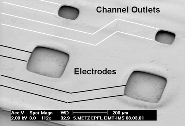 | ||
| Fig. 7 SEM image of the active area of a microelectrode with recording/stimulation electrodes (200 × 200 μm2) and fluidic outlets (100 × 100 μm2) for local delivery of a bioactive fluid with good spatial resolution. The embedded channels and metallization lines are not visible in the picture. Their position has been illustrated by drawing black and white lines on the picture. | ||
Furthermore, microchannels with electrodes inside the channels can be fabricated. These devices can be used in the field of electrochemical research10 or for the detection of particles flowing through the channel.20 An example is illustrated in Fig. 8, showing three metallization lines (width 50 μm and 250 nm thickness) and a channel of 100 μm width with an electrode at the bottom of the channel.
 | ||
| Fig. 8 Cross-section of a polyimide device with three adjacent interconnection lines (left side) and a microchannel (width 100 μm, height 20 μm) with an electrode inside the channel (right side). | ||
Discussion
The key principle of this adapted lamination method is to utilize the chemical reaction of the polyimide curing process. Semi-cured polyimide films are subsequently converted to fully imidized polyimide by thermal cure. This principle is also applied for the production of multichip-modules (MCM) by spincoating precursor solutions to form a film, and then soft-baking these films to cause them to partially convert to the imidized form, before spinning on a second layer. Since the second layer is spun onto a partially imidized layer, the chains will interpenetrate and yield a strong interface.21Polyimide-based microfluidic devices as presented above can potentially suffer from leakage when debonding occurs at the polyimide–polyimide interfaces. It has been shown that polyimide–polyimide adhesion can be considerably improved by increasing the interdiffusion distance between two layers.21,22 Interdiffusion across the interface, which allows polymer chains to entangle with each other, was identified as the main mechanism of adhesion. It was found that a large diffusion distance, at least 200 nm, is required to obtain a bond whose strength is equal to that of the bulk material. The degree of interdiffusion is primarily determined by the cure temperature of the two layers and is favored by a low first layer cure temperature and a high second layer cure temperature.21 It is therefore critical to adapt curing cycles to obtain high bond strength between subsequent polyimide layers. We found that best results can be obtained if the first layer is cured at a temperature between 100 and 150 °C followed by a second cure after the cover layer has been laminated with a temperature higher than 300 °C. Secondly, adhesion-strengthening interdiffusion can also be increased by the structural and rheological changes brought about in the underlayer by the sorption of a strong solvent,22 which acts as a swelling agent. In the case of polyimide, the choice of NMP as a solvent was a natural one, since it is the primary solvent in the polyamic acid solution. The swelling agent is removable, since the NMP is completely desorbed during the cure of the second polyimide layer. Depending on the desired swelling effect, the first layer can be immersed in NMP from minutes to hours and at increased temperatures. A prolonged exposure to NMP at high temperatures results in good adhesion even if the first polyimide layer has been cured at temperatures higher than 150 °C.
While Frazier’s method11 relied upon residual solvent, the method by Glasgow14 bakes out most of the solvent, and a small controlled quantity of solvent solution containing polyimide precursor is added at the interface. Solvent evaporation during final cure is difficult as the fabricated channels are located between two wafers. The correct trade-off for the right amount of solvent to add is hard to achieve in order to avoid unbonded areas, channel blocking, bubbles or voids. Glasgow’s technique yields rigid channels, as the fabrication process uses a glass cover with polyimide spun-on to be bonded to the open channel structures. Therefore, high quality bonds depend also upon the flatness and stiffness of the substrate. If both substrates are thick, good contact across most of the interface requires the substrates to be very flat. In our case, only a thin Mylar™ foil is covering the transferred polyimide layer during lamination. The layer can conform and ensure good contact throughout the interface. The solvent swells the polyimide layer, which also encourages contact between the layers.
The method proposed by Mangriotis15 adds a controlled quantity of solvent solution containing polyimide precursor as adhesion layer at the interface between the partially cured polyimide and the Kapton sheet. It was shown that the lamination of fully cured Kapton films with an intermediate layer of spin-coated polyimide precursor yields weaker interfaces compared to laminating an only partially imidized layer. Stoffel et al. were able to form a strong laminate structure by modifying the surface of the Kapton™ base film, causing the region within 200 nm of the surface to reconvert to polyamic acid (polyimide precursor).23 A layer in contact with this modified film will result in a diffuse interface between the base film and the laminated film. The laminated film will diffuse to the depth of the modified polyamic acid layer. This surface modification corresponds to our situation where the polyimide is only partially imidized on both sides of the interface.
The adapted lamination and layer transfer technique employs a second carrier substrate to prepare the cover layer. After detaching the second substrate and the Mylar™ foil, the laminated layer can be structured by photolithography or dry etching techniques to open the channel inlet and outlet ports. Via those channel openings, solvent can evaporate during the final cure to avoid high internal pressures, which can cause debonding. Mylar™ foils were found to be an appropriate material as they adhere well to the support wafer during spinning. After lamination, the foils can be easily detached from the polyimide since their adherence was merely from surface tension and not via a crosslinking mechanism. We have successfully laminated polyimide layers on various substrates, such as glass, silicon, aluminium, and over the entire wafer size we observed no voids or bubbles.
Polyimide cover layer thickness and softbake parameters can be adapted to obtain optimum results for the lamination. If the prepared layer is softbaked for too long, the residual solvent content is too low and it can delaminate after the lamination step. A minimum adhesion of the laminated layer is necessary to perform the photolithography or dry etching step. If the softbake is too short, the polyimide precursor remains partly liquid and can potentially fill up the channels. It must be noted that the softbake step has to be carried out at moderate temperatures and extended softbake times to avoid water vapor between the Mylar™ foil and the second carrier substrate. Otherwise, the Mylar™ foil will start to detach from the carrier substrate and buckle, leading to a non-uniform softbake.
The polyimide–polyimide bond strengths have not yet been quantified. The bond strength has been qualitatively evaluated by trying to detach a laminated polyimide layer. For that purpose, a silicon substrate was spin-coated with a first polyimide layer after applying an adhesion promoter. This first polyimide layer was then partially cured and treated with NMP as outlined above. By using the layer transfer and lamination technique, we covered this first layer with a laminated, second layer. A part of the wafer was not laminated to serve as starting point for the de-lamination of the second polyimide layer. The samples were then cured as described previously. The de-lamination of the second polyimide layer was not possible before rupture of the film, indicating that the adhesion strength is comparable to the properties of the bulk material. We are currently working on a quantitative analysis of the bond strengths between laminated polyimide layers.
A metallization layer can easily be combined with the polyimide structures. For gold or platinum metallizations, a titanium or chrome adhesion layer is required. In appropriate post-processing steps, electrode surfaces can be altered, for example, by covering with porous platinum or activated iridium oxide films to improve impedance characteristics. Silver electrodes inside channels can be electrochemically modified to Ag/AgCl reference electrodes for electrophysiological measurements in biosciences.
From contact angle observations of de-ionized water drops on polyimide and from the capillary behavior, we conclude that our polyimide-based devices are moderately hydrophilic. However, the surface energy of polyimide can be altered by plasma processing techniques. An increased hydrophobicity is accomplished by a nitrogen trifluoride plasma,24 where fluorine is introduced into the surface of the polyimide. In contrast to that, an oxygen plasma treatment will increase the hydrophilic character of the polyimide.25
Conclusion
The design and fabrication of polyimide-based microfluidic devices have been described, basic flow characteristics of the microchannels evaluated and burst pressure tests performed. The described fabrication technology offers advantages over previously reported methods. The laminated polyimide sheet can be photostructured to form the channel top layer and provide channel access holes. Due to the open channel ports, the solvents present in the polyimide precursor can escape during the final cure avoiding high internal pressures that can cause bonding failure. Furthermore, cure cycles can be adapted to increase interdiffusion between partially cured polyimide layers, which are subsequently bonded. A swelling agent surface treatment can additionally be used to increase bond strength. The polyimide–polyimide bond strengths were found to be roughly comparable to the bulk properties. By combining the lamination technique with other well-known process steps, such as the introduction of a metallization layer, versatile devices can be fabricated. With these two technologies, most of the demands for lab-on-a-chip applications can be met. The microdevices consist entirely of polyimide, except where electrodes are incorporated inside the channels. Polyimides are well known for their good mechanical and electrical material properties and are increasingly examined for applications other than passivation layers in microelectronics. Furthermore, the process is compatible with integrated circuit processing technology and integrated sensor fabrication, and thus many integrated microsystems can be envisioned.Acknowledgement
This work was founded by the Leenaards Foundation within the project ‘Hearing and talking to the neuronal network of a living insect using an implantable microprocessor-based device.’ Clean room processing was done at the EPFL Center for Microtechnology (CMI) with the support of Ph. Flückiger, C. Hibert, G.-A. Racine, G. Clerc, Y. Deillon, W. Baer, I. Magnenat and J. M. Voirol.References
- D. C. Duffy, J. C. McDonald and O. J. A. Schueller, Anal. Chem., 1998, 70, 4974 CrossRef CAS.
- P. M. Martin, D. W Matson, W. D. Bennett and D. J. Hammerstrom, Proc. SPIE, 1998, 3515, 172 Search PubMed.
- M. O. Heuschkel, L. Guerin, B. Buisson, D. Bertrand and P. Renaud, Sens. Actuators, B, 1998, B48, 356 CrossRef.
- N. F Raley, J. C. Davidson and J. W. Balch, Proc. SPIE, 1995, 2639, 40 Search PubMed.
- M. Stjernstrom and J. Roeraade, J. Micromech. Microeng., 1998, 8, 33 CrossRef CAS.
- J. Brazzle, I. Papautsky and A. B. Frazier, IEEE Eng. Med. Biol. Mag., 1999, 18, 53 CrossRef CAS.
- J. C. Selby and M. A. Shannon, Technical Digest. Solid State Sensor and Actuator Workshop. Transducer Research Foundation, Cleveland, OH, USA, 1998, pp. 252–5 Search PubMed.
- H. J. Suh, P. Bharathi, D. J. Beebe and J. S. Moore, J. Microelectromech. Syst., 2000, 9, 198 CrossRef CAS.
- K. Walsh, J. Norville and T. Yu. Chong, presented at 14th IEEE International Conference on Micro Electro Mechanical Systems, Interlaken, Switzerland, 2001, pp. 114–7..
- J. S. Rossier, M. A. Roberts, R. Ferrigno and H. H. Girault, Anal. Chem., 1999, 71, 4294 CrossRef CAS.
-
A. B. Frazier, presented at 38th Midwest Symposium on Circuits and Systems, Rio de Janeiro, Brazil, 1996, pp. 505–8.
![[*]](https://www.rsc.org/images/entities/char_e103.gif) The paper outlines a wafer-to wafer bonding technique with embedded microchannels, which uses polyimide as adhesive.
The paper outlines a wafer-to wafer bonding technique with embedded microchannels, which uses polyimide as adhesive. - R. R. Richardson, J. A. Miller and W. M. Reichert, Biomaterials, 1993, 14, 627 CrossRef CAS.
- C. Goll, W. Bacher, B. Bustgens, D. Maas, W. Menz and W. K. Schomburg, J. Micromech. Microeng., 1996, 6, 77 CrossRef CAS.
- I. K. Glasgow, D. J. Beebe and V. E. White, Sensors-and-Materials, 1999, 11, 269 Search PubMed .
This paper describes a solvent bonding technique where microfluidic devices are fabricated between two wafers. Open channels are patterned on a first wafer, a second wafer is spin-coated with polyimide precursor and the two wafers are put in contact and bonded together in a vacuum oven.
-
M. D. Mangriotis, S. S. Mehendale, T. Z. Liu, A. M. Jacobi, M. A. Shannon and D. J. Beebe, presented at 10th International Conference on Solid-State Sensors and Actuators, Transducers ′99, Sendai, Japan, 1999, pp. 772–5.
This paper outlines a layer transfer technique where a fully cured Kapton™ foil is bonded to the open channel structures by using a thin layer of polyimide precursor as adhesive.
- M. Datta, IBM J. Res. Dev., 1993, 37, 207 Search PubMed.
- B. H. Jo, L. M. Van Lerberghe, K. M. Motsegood and D. J. Beebe, J. Microelectromech. Syst., 2000, 9, 76 CrossRef CAS.
- C. Trautmann, W. Bruechle, R. Spohr, J. Vetter and N. Angert, Nucl. Instrum. Methods Phys. Res., Sect. B , 1996, B111, 70 CrossRef.
- S. Metz, F. Oppliger, R. Holzer, B. Buisson, D. Bertrand and P. Renaud, presented at IEEE EMBS Special Topic Conference on Microtechnology in Medicine and Biology, Lyon, France, 2000, pp. 619–23.
- S. Gawad, M. Wütherich, L. Schild, O. Dubochet and P. Renaud, presented at 11th International Conference on Solid-State Sensors and Actuators, Munich, Germany, 2001, pp. 1190–3.
- H. R. Brown, A. C. M. Yang, T. P. Russell, W. Volksen and E. J. Kramer, Polymer, 1988, 29, 1807 CrossRef CAS . This paper illustrates the importance of cure cycle adaptation between polyimide layers to improve adhesion. Good adhesion results from a low cure temperature of the first layer followed by a higher cure temperature of the final layer sandwich.
- K. L. Saenger, H. M. Tong and R. D. Haynes, J. Polym. Sci., Part C: Polym. Lett., 1989, 27, 235 Search PubMed .
This paper outlines the influence of swelling agent treatment of polyimide layers before lamination. Adhesion strengthening can be fostered by the sorption of a strong solvent.
- N. C. Stoffel, M. Hsieh, E. J. Kramer and W. Volksen, IEEE Trans. Compon., Packag., Manuf. Technol., Part B:, 1996, 19, 417 Search PubMed .
The paper reports on the formation of strong polyimide laminates by modifying the surface of a Kapton™ base film, causing the region within
200 nm of the surface to reconvert to polyamic acid (polyimide precursor). A layer in contact with this modified film will result in a diffuse interface between the base film and the laminated film leading to high bond strengths after the cure.
- M. A. Petrich and H. Y. Lu, Materials Science of High Temperature Polymers for Microelectronics Symposium, Materials Research Society, Pittsburgh, PA, USA, 1991, pp. 323–8 Search PubMed.
- B. R. Zhu, H. Iwata, I. Hirata and Y. Ikada, J. Adhes. Sci. Technol., 2000, 14, 351 Search PubMed.
| This journal is © The Royal Society of Chemistry 2001 |