
CdS/CdSe co-sensitized 3D SnO2/TiO2 sea urchin-like nanotube arrays as an efficient photoanode for photoelectrochemical hydrogen generation†
Cheng Li,
Haifeng Zhang and
Chuanwei Cheng*
Shanghai Key Laboratory of Special Artificial Microstructure Materials and Technology, School of Physics Science and Engineering, Tongji University, Shanghai 200092, P. R. China. E-mail: cwcheng@tongji.edu.cn
First published on 30th March 2016
Abstract
In this paper, we report a novel electrode of 3D ordered CdS/CdSe co-sensitized sea urchin-like SnO2/TiO2 nanotube arrays for photoelectrochemical hydrogen production. This novel photoanode presents excellent PEC performance, yielding a maximum photocurrent density of ∼6 mA cm−2 at 1.4 V vs. RHE under light illumination AM 1.5 (100 mW cm−2), which is due to the 3D structural effect of the SnO2/TiO2 sea urchin nanotubes, stepwise cascade band alignment between SnO2/TiO2 and CdS/CdSe as well as the improvement of light harvesting in the visible region.
The utilization of photoelectrochemical (PEC) cells that convert solar energy into hydrogen fuel is a promising way to address the world's increasing energy demand as well as the reduction of the CO2 emission.1–4 The PEC water splitting processes consist of four main steps, i.e., light absorption, charge separation, charge transport and the charge recombination process.5 As such, an ideal photoelectrode should process high specific surface area, excellent charge transport and light harvesting ability. Since the innovative report on photocatalysis of water splitting using TiO2–Pt system,6 great effort has been devoted to design novel electrodes with tailored nanostructures in order to boost the efficiency.7–11 For instance, 1D nanowires,12 nanotubes,13 3D branched nanowires14,15 and 3D urchin structured photoelectrodes have been explored.16,17 Especially, 3D sea urchin structures that combine both 3D hollow spheres and 1D building blocks are particularly attractive due to their high specific surface area and strong light scattering ability.16–19 SnO2 with wide band gap (3.6 eV) and high electron mobility (100–200 cm2 V−1 S−1) in contrast to TiO2 (∼0.1–1 cm2 V−1 S−1) is a promising candidate for optoelectronic devices. Moreover, the type II band alignment between SnO2 and TiO2 makes the SnO2/TiO2 composite to be very attractive in solar cells,20–22 photocatalysis23 and water splitting application.24,25 Besides, coupling metal oxide semiconductor with narrow band gap sensitiser such as CdS26,27 and/or CdSe28–31 is an effective approach to improve the conversion efficiency by improving the light harvesting ability in the visible region.
Herein, we report an innovative electrode of 3D SnO2/TiO2 sea urchin-like nanotube arrays by combination of ZnO sea urchin structures as templates and atomic layer deposition of SnO2 and TiO2 for the first time. The hollow sea urchin nanotube structures might be more beneficial for quantum dots loading and electrolyte infiltration in contrast to that of nanowires structures. CdS and CdSe quantum dots are further used as co-sensitizer for extending the visible light absorption edge. PEC measurements demonstrate that CdS/CdSe co-sensitized 3D SnO2/TiO2 sea urchin-like nanotubes electrode presents the best performance in contrast to that of SnO2/TiO2 sea urchin-like nanotubes and only CdS sensitized one.
The 3D SnO2/TiO2 sea urchin like nanotubes arrays were fabricated by using the SnO2 hollow spheres/ZnO nanorods sea urchins as sacrificial templates and subsequent ALD deposition of SnO2 and TiO2 layer. The fabrication process is illustrated in Fig. S1† and the typical SEM images of SnO2/ZnO urchins are presented in Fig. S2.† It can be seen that the ZnO nanorods are radially grown on the surfaces of each microsphere, forming a periodical sea urchin pattern in a large area. After the ALD deposition of SnO2 and TiO2 and removal of ZnO templates, the SnO2/TiO2 nanotube sea urchin-like arrays were obtained. As shown in Fig. 1a, perfectly patterned sea urchin arrays are still reserved. From a high-magnification view in Fig. 1b, the overall diameter of individual SnO2/TiO2 nanotube sea urchin is about 5 μm. The SEM images of SnO2/TiO2 sea urchin-like nanotubes after CdS quantum dots sensitization and CdS/CdSe co-sensitization are displayed in Fig. 1c–f, respectively, it can be observed the quantum dots layer are uniformly coated on the nanotubes surfaces, without influencing the periodical characteristics. Besides, no obvious nanoparticles aggregation was observed. Further EDX measurement (Fig. S3†) confirms the chemical elements in CdS/CdSe sensitized SnO2/TiO2 sea urchin nanotube arrays.
 | ||
| Fig. 1 SEM images of (a and b) 3D SnO2/TiO2 sea urchin-like nanotubes; CdS sensitized (c and d) and CdS/CdSe co-sensitized (e and f) 3D sea SnO2/TiO2 urchin-like nanotubes. | ||
The microstructures of the SnO2/TiO2 urchin-like nanotubes and quantum dots sensitized samples were further characterized by transmission electron microscopy (TEM) and HRTEM. The typical TEM image of SnO2/TiO2 nanotubes in Fig. 2a clearly demonstrates the core/shell hybrid nanotube morphology. From the TEM image (inset of Fig. 2a), it can be seen that the tube wall thickness of SnO2 and TiO2 are ∼10 nm and ∼5 nm, respectively. The HRTEM image of SnO2/TiO2 nanotube in Fig. 2b indicates that the SnO2 is crystalline. The measured lattice 0.24 nm is corresponding to the (200) plane of rutile phase of SnO2. The TEM and HRTEM image in Fig. 2c and d represent the structure of CdS sensitized SnO2/TiO2 urchin-like nanotubes, indicating that the CdS layer is distributed uniformly on the surface of the SnO2/TiO2 nanotube. As shown in Fig. 2d, a clear interface between CdS and TiO2 can be observed. The measured lattices 0.34 nm is corresponding to the (002) plane of CdS. The thickness of CdS layer is about 8 nm. Fig. 2e and f show the TEM and HR-TEM image of the of CdS/CdSe co-sensitized SnO2/TiO2 urchin-like nanotubes, suggesting that CdSe nanoparticles were deposited on the surface successfully. As shown in Fig. 2f, the measured lattice of 0.34 nm and 0.22 nm are corresponding to the (002) plane of CdS and the (110) plane of CdSe.
 | ||
| Fig. 2 TEM and HR-TEM images of (a and b) 3D SnO2/TiO2 sea urchin-like nanotubes, inset of (a) is individual SnO2/TiO2 nanotube; CdS sensitized (c and d) and CdS/CdSe co-sensitized (e and f) 3D SnO2/TiO2 sea urchin-like nanotubes. | ||
To further investigate the composition and chemical environment of the as-fabricated CdS/CdSe co-sensitized SnO2/TiO2 urchin-like nanotubes, X-ray photoelectron spectroscopy (XPS) was performed. The high-resolution XPS spectra in Fig. 3a shows the O peaks that were divided into three peaks with binding energy at 530.0, 530.4 and 533.3 eV, which may be ascribed to the Sn–O in SnO2,32 Ti–O in TiO2,33 and hydroxyl groups, respectively. The two peaks in Fig. 3b were corresponding to the Ti 2p3/2 and Ti 2p1/2 with binding energies of 458.8 and 464.7 eV.33 The spectra of Sn 3d in Fig. 3c shows two peaks of Sn 3d3/2 and Sn 3d5/2 with binding energies centered at 486.6 and 495.1 eV, respectively.32 As shown in Fig. 3d, the Cd 3d5/2 peak centered at 405.1 eV and the Cd 3d3/2 peak centered at 411.8 eV.33 The two peaks in Fig. 3e were corresponding to the S 2p3/2 and S 2p1/2 with binding energies of 160.1 and 161.5 eV, indicating that the valence state of S is −2.34 The two peaks centered at 53.9 and 54.8 eV in Fig. 3f are associated with the Se 3d5/2 and Se 3d3/2, which may be ascribed to the Cd–Se bonds.35
 | ||
| Fig. 3 XPS spectra collected from CdS/CdSe co-sensitized 3D SnO2/TiO2 sea urchin-like nanotubes. (a) O 1s; (b) Ti 2p; (c) Sn 3d; (d) Cd 3d; (e) S 2p; (f) Se 3d. | ||
The optical characteristics of the as-fabricated CdS and CdS/CdSe sensitized SnO2/TiO2 sea urchin-like nanotubes were studied by collecting the diffuse light reflectance spectrum with UV-vis spectrophotometer. As shown in Fig. 4, the CdS/CdSe co-sensitized SnO2/TiO2 sea urchin-like nanotubes exhibits the best light harvesting ability in the whole measured wavelength scale in contrast to that of SnO2/TiO2 and CdS sensitized one. The absorption edge is extending to ∼650 nm, corresponding to the bandgap of CdSe quantum dots, which is improving the visible light harvesting ability greatly.
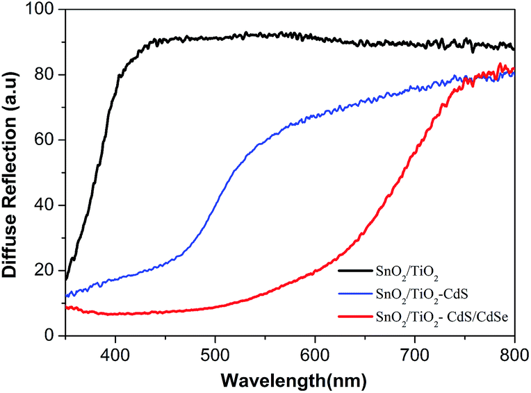 | ||
| Fig. 4 UV-vis diffuse reflectance spectrum of 3D SnO2/TiO2 urchin-like nanotubes, CdS sensitized and CdS/CdSe co-sensitized 3D SnO2/TiO2 urchin-like nanotubes. | ||
The PEC water splitting performance was evaluated by measuring the photocurrent density with a three-electrode electrochemical cell. Fig. 5a presents a group of the linear sweep voltammogram curves collected from SnO2/TiO2, CdS sensitized and CdS/CdSe co-sensitized SnO2/TiO2 sea urchin-like nanotubes photoanodes measured in the dark and under light illumination (AM 1.5, 100 mW−2). It can be seen that all the three samples present very small current density in the dark, while under light illumination, pronounced photocurrent density were observed, especially for the CdS and CdS/CdSe co-sensitized samples. It is worthy noting that the CdS/CdSe co-sensitized SnO2/TiO2 sea urchin-like nanotubes photoelectrode shows the best PEC performance, achieving a maximum photocurrent density of ∼6 mA cm−2 at 1.4 V vs. RHE, which is 15 times and 2 times larger than that of bare SnO2/TiO2 sea urchin-like nanotubes (0.4 mA cm−2) and CdS sensitized one (3 mA cm−2), respectively. The achieved photocurrent density value is also superior to most of the previous reported results in quantum dots sensitized photoelectrodes, such as CdS sensitized TiO2/ZnO urchins (∼3.6 mA cm−2),13 CdS sensitized TiO2 inverse opals (4.84 mA cm−2),4 ZnSe/CdS/CdSe triple-sensitized ZnO nanowire arrays (∼5.3 mA cm−2),36 and CdS/CdSe sensitized hollow TiO2 nanowire arrays (∼4 mA cm−2).37 This might be attributed to the 3D structural effect of SnO2/TiO2 sea urchin-like nanotubes that provides large surface area for quantum dots loading as well as the synergistic effect of CdS and CdSe quantum dots which improves the visible light absorption and charge transfer process. Fig. 5b presents the corresponding transient i–t curves of the three photoelectrodes collected under chopped light illumination (30 s every light/dark cycle) at the bias of 0.9 V vs. RHE, demonstrating excellent photoresponse ability and fast photoswitching property. What's more, the CdS/CdSe co-sensitized SnO2/TiO2 sea urchin-like nanotubes photoelectrode showed very excellent photo-stability with little decay under continuous light illumination, as shown in Fig. 5c.
 | ||
| Fig. 5 (a) Linear sweep voltammograms of different photoanodes measured under light illumination (AM 1.5, 100 mW cm−2) and in the dark. (b) Transient i–t curves of different photoanodes at a fixed bias of 0.9 V vs. RHE under chopped light irradiation (on/off cycles of 30 s). (c) Light stability test at a fixed bias of 0.9 V vs. RHE under light illumination (AM 1.5, 100 mW cm−2). (d) EIS spectra of 3D SnO2/TiO2 sea urchin-like nanotubes, CdS sensitized and CdS/CdSe co-sensitized 3D SnO2/TiO2 sea urchin-like nanotubes. | ||
To understand the charge transfer mechanism of CdS/CdSe sensitized SnO2/TiO2 sea urchin-like nanotubes, electrochemical impedance spectroscopy (EIS) measurement was conducted at open-circuit condition under simulated light illumination. Fig. 5d presents the Nyquist plots of the collected EIS data, which can be fitted by the physical model developed in similar quantum dots sensitized heterostructures.37,38 The semicircle in the high frequency (>104 Hz) in the Nyquist plots corresponds to the charge transfer in TiO2/FTO interface, while the second semicircle portion in the middle frequency range (1–103 Hz) corresponds to the charge transfer resistance at the photoelectrode/electrolyte interface. Apparently, the CdS/CdSe sensitized SnO2/TiO2 urchin-like nanotubes photoanode shows the smallest charge transfer resistance in contrast to that of SnO2/TiO2 and CdS sensitized one, which suggests that the stepwise cascade band alignment between CdS/CdSe and SnO2/TiO2 (as illustrated in Fig. 6b) are facilitating the photo-induced charge separation and transfer process.
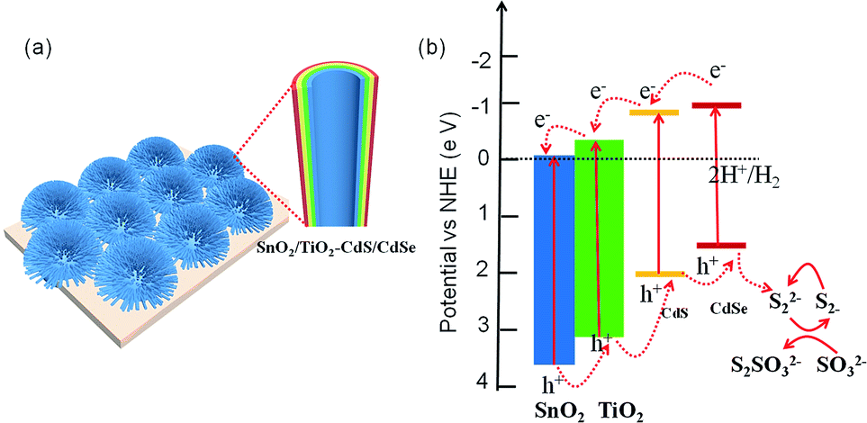 | ||
| Fig. 6 (a) Scheme of the CdS/CdSe co-sensitized of SnO2/TiO2 sea urchin-like nanotube arrays. (b) Band alignment and charge transfer process between the CdS/CdSe and SnO2/TiO2. | ||
The scheme of urchin-like nanotubes arrays and processes of electron transfer in the CdS/CdSe co-sensitized SnO2/TiO2 urchin-like nanotubes photoelectrode can be simplified in Fig. 6a and b. As shown in Fig. 6b, under light illumination, the semiconductor SnO2/TiO2 and QDs absorb the photons and generated electron–hole pairs. Compared with SnO2 and TiO2, CdS has a higher conduction band edge, CdSe has a higher valence band edge, which is advantageous to the charge transportation.31 The stepwise cascade band alignment between the CdS/CdSe and SnO2/TiO2 is facilitating the photo-induced carrier separation and transfer process, as a result in reduction in the electron-holes recombination process. The higher electron mobility of SnO2 nanotubes would be beneficial for improving the charge collection efficiency.24
Based on the above discussions, the excellent PEC performance for 3D CdS/CdSe co-sensitized TiO2/SnO2 electrode can be explained as follows. First, the 3D urchin-like TiO2/SnO2 electrode provided increased surface area for both CdS and CdS quantum dots loading, leading to an enhancement of light harvesting, as evidenced in Fig. 4. Second, the stepwise cascade band alignment between the CdS/CdSe and SnO2/TiO2 is beneficial for the charge separation and transfer process, result in improving the charge separation and collection efficiency.
Conclusions
In summary, we have fabricated a novel three-dimensional sea urchin-like SnO2/TiO2 nanotube arrays photoelectrode by ALD route using ZnO sea urchin as a sacrificial template. The 3D SnO2/TiO2 composite nanotubes design provides increased surface area for CdS and CdSe quantum dots loading and improved charge collection efficiency due to the higher electron mobility of SnO2. The as-fabricated CdS/CdSe co-sensitized SnO2/TiO2 urchin-like nanotubes exhibited excellent photoelectrochemical performance, which is attributed to the improved light harvesting ability by CdS and CdSe and stepwise cascade band alignment between SnO2/TiO2 and CdS/CdSe that facilitates the charge separation and transfer processes. Our approaches may open up new opportunity for design of other multi-components semiconductor electrode for high-efficiency PEC water splitting application.Experimental section
Fabrication of SnO2/TiO2 sea urchin-like nanotube arrays
The 3D SnO2/TiO2 sea urchin-like nanotube arrays were prepared by using ZnO urchin as a sacrificial template combined with atomic layer deposition (ALD) technique. In a typical process: first, the ZnO urchin arrays on FTO substrate were fabricated with a colloid spheres templates and hydrothermal growth route according to our previous reports.16 The ALD SnO2/ZnO coated PS microspheres substrate was immersed into a 35 mL aqueous solution of equimolar zinc nitrate (Zn(NO3)2·6H2O) (0.025 M) and hexamethylenetetramine (C6H12N4) in an autoclave. The reaction was conducted at 95 °C for 3 h. Subsequently, the ZnO urchin arrays were deposited with 10 nm of SnO2 and 5 nm of TiO2 by atomic layer deposition system (Picosun SUNALE R-200). The tin tetrachloride, titanium tetrachloride and H2O were used as Sn, Ti and O precursors, respectively. During the reaction, the reaction chamber was kept at 1.0 mbar with a steady N2 gas at 200 sccm (cubic centimeter per minute) and the deposition temperature was 350 °C. Finally, the as-prepared films were immersed in NH3·H2O for 24 h to remove the ZnO templates, forming the 3D SnO2/TiO2 urchin-like nanotube arrays.Fabrication of CdS/CdSe Co-sensitized SnO2/TiO2 sea urchin nanotube arrays
CdS and CdSe quantum dots were sensitized on the 3D SnO2/TiO2 sea urchin nanotube arrays using a successive ionic layer adsorption and reaction (SILAR) method.4 First, 3 layers of CdS quantum dots were assembled by immersing the substrates Cd(Ac)2 ethanol solution (0.1 M) for 1 min, followed by immersing in the Na2S methanol solution (0.1 M) for 1 min, rinsed with methanol and water respectively, then dried under N2 stream. This procedure was repeated 3 times. Then CdSe quantum dots were deposited with the Cd(NO3)2 and Na2SeSO3 as the Cd and Se source, respectively. The Na2SeSO3 aqueous solution was prepared by stirring and refluxing 0.3 M Se and 0.6 M Na2SO3 at 70 °C until the solution is clear. The CdS sensitized samples were immersed in Cd(NO3)2 ethanol solution for 1 min, rinsed with ethanol, dried under N2 stream, then kept immersing in the Na2SeSO3 aqueous solution at 50 °C for 30 min. This procedure was repeated 5 times for a desirable thickness.Characterizations
The structures and morphology of as-obtained products were characterized by FEI Sirion200 emission scanning electron microscopy (FE-SEM) and JEM 2010F transmission electron microscope (TEM). The diffuse reflectance spectrum was collected by UV-vis spectrophotometer (Hitachi, U3900 H) with an integration sphere.Photoelectrochemical measurements
The PEC properties were measured by a electrochemical workstation (CHI760D, CHI instrument) using three-electrode electrochemical cell, where Pt foil, Ag/AgCl electrode and the as-prepared products serve as the counter electrode, reference electrode and working electrode, respectively. A mixed aqueous solution that contains 0.25 M Na2S and 0.35 M Na2SO3 was used as electrolyte. The PH value was around 12.5, and all the measurements were referred to the reversible hydrogen electrode (RHE) by the equation VRHE = VAg/AgCl + 0.197 + 0.059pH. A 150 W Xe lamp (Zolix SS150) with an AM 1.5 G filter which was calibrated by a standard Si solar cell was used as the light source. Time-dependent photo-response tests were carried out at bias of 0.9 V vs. RHE under chopped light irradiation (30 s every light/dark cycle). The electrochemical impedance spectroscopy (EIS) was obtained at open-circuit condition under simulated light illumination in a three-electrode configuration with a frequency range from 0.1 Hz to 1000 kHz.Acknowledgements
This work was financially supported by 973 Program (Grant no. 2013CB632701), the National Natural Science Foundation of China (Grant no. 51202163) and Doctor Programs Foundation of MOE (20120072120044).Notes and references
- A. J. Bard and M. A. Fox, Acc. Chem. Res., 1995, 28, 141 CrossRef CAS.
- M. G. Walter, E. L. Warren, J. R. McKone, S. W. Boettcher, Q. X. Mi, E. A. Santori and N. S. Lewis, Chem. Rev., 2010, 110, 6446 CrossRef CAS PubMed.
- K. Maeda and K. Domen, J. Phys. Chem. Lett., 2010, 1, 2655 CrossRef CAS.
- C. W. Cheng, S. K. Karuturi, L. J. Liu, J. P. Liu, H. X. Li, L. T. Su, A. I. Y. Tok and H. J. Fan, Small, 2012, 8, 37 CrossRef CAS PubMed.
- F. E. Osterloh, Chem. Soc. Rev., 2013, 42, 2294 RSC.
- A. Fujishima and K. Honda, Nature, 1972, 238, 37–38 CrossRef CAS PubMed.
- B. D. Alexander, P. J. Kulesza, I. Rutkowska, R. Solarska and J. Augustynski, J. Mater. Chem., 2008, 18, 2298 RSC.
- S. C. Warren and E. Thimsen, Energy Environ. Sci., 2011, 9, 5133 Search PubMed.
- Z. S. Li, W. J. Luo, M. L. Zhanag, J. Y. Feng and Z. G. Zou, Energy Environ. Sci., 2013, 6, 347 CAS.
- C. W. Cheng and Y. Sun, Appl. Surf. Sci., 2012, 263, 273 CrossRef CAS.
- Y. J. Hwang, A. Boukai and P. Yang, Nano Lett., 2009, 9, 410 CrossRef CAS PubMed.
- S. W. Boettcher, J. M. Spurgeon, M. C. Putnam, E. L. Warren, D. B. Turner-Evans, M. D. Kelzenberg, J. R. Maiolo, H. A. Atwater and N. S. Lewis, Science, 2010, 327, 185 CrossRef CAS PubMed.
- Z. Zhang and P. Wang, Energy Environ. Sci., 2012, 5, 6506 CAS.
- A. Kargar, K. Sun, Y. Jing, C. Choi, H. Jeong, G. Y. Jung, S. Jin and D. Wang, ACS Nano, 2013, 7, 9407 CrossRef CAS PubMed.
- I. S. Cho, Z. B. Chen, A. J. Forman, D. R. Kim, P. M. Rao, T. F. Jaramillo and X. L. Zheng, Nano Lett., 2011, 11, 4978 CrossRef CAS PubMed.
- C. W. Cheng, H. F. Zhang, W. N. Ren, W. J. Dong and Y. Sun, Nano Energy, 2013, 2, 779–786 CrossRef CAS.
- W. N. Ren, H. F. Zhang, D. Z. Kong, B. Liu, Y. P. Yang and C. W. Cheng, Phys. Chem. Chem. Phys., 2014, 16, 22953 RSC.
- J. Elias, C. Lévy-Clément, M. Bechelany, J. Michler, G.-Y. Wang, Z. Wang and L. Philippe, Adv. Mater., 2010, 22, 1607 CrossRef CAS PubMed.
- D.-M. Tang, G. Liu, F. Li, J. Tan, C. Liu, G. Q. Lu and H. M. Cheng, J. Phys. Chem. C, 2009, 113, 11035 CAS.
- S. H. Ahn, D. J. Kim, W. S. Chi and J. H. Kim, Adv. Funct. Mater., 2014, 24, 5037 CrossRef CAS.
- U. V. Desai, C. Xu, J. Wu and D. Gao, J. Phys. Chem. C, 2013, 115, 3232 Search PubMed.
- A. Thapa, J. T. Zai, H. Elbohy, P. Poudel, N. Adhikari, X. F. Qian and Q. Q. Qiao, Nano Res., 2014, 7, 1154 CrossRef CAS.
- J. G. Yu, Y. Wang and W. Xiao, J. Mater. Chem. A, 2013, 1, 10727 CAS.
- C. W. Cheng, W. N. Ren and H. F. Zhang, Nano Energy, 2014, 5, 132 CrossRef CAS.
- C. T. Gao, Z. M. Zhang, X. D. Li, L. L. Chen, Y. Q. Wang, Y. M. He, F. Teng, J. Y. Zhou, W. H. Han and E. Q. Xie, Sol. Energy Mater. Sol. Cells, 2015, 141, 101 CrossRef CAS.
- W. T. Sun, Y. Yu, H. Y. Pan, X. F. Gao, Q. Chen and L. M. Peng, J. Am. Chem. Soc., 2008, 130, 1124 CrossRef CAS PubMed.
- S. K. Karuturi, C. W. Cheng, L. Liu, L. T. Su, H. J. Fan and A. I. Y. Tok, Nano Energy, 2012, 1, 322 CrossRef CAS.
- H. Jennifer, G. M. Wang, Y. Li and J. Z. Zhang, Nano Lett., 2010, 10, 478 CrossRef PubMed.
- J. Y. Xiao, Q. L. Huang, J. Xu, C. H. Li, G. P. Chen, Y. H. Luo, D. M. Li and Q. B. Meng, J. Phys. Chem. C, 2014, 118, 4007 CAS.
- Z. Ali, I. Shakir and D. J. Kang, J. Mater. Chem. A, 2014, 2, 6474 CAS.
- Y.-L. Lee, C.-F. Chi and S.-Y. Liau, Chem. Mater., 2010, 22, 922 CrossRef CAS.
- L. B. Luo, F. X. Liang and J. S. Jie, Nanotechnology, 2011, 22, 485701 CrossRef PubMed.
- Z. Chen and Y. J. Xu, ACS Appl. Mater. Interfaces, 2013, 5, 13353 CAS.
- N. Zhang, S. Q. Liu, X. Z. Hu and Y.-J. Xu, J. Mater. Chem., 2012, 22, 5042 RSC.
- S. Das, B. Satpati, H. Chauhan, S. Deka, C. Gopinath and T. Bala, RSC Adv., 2014, 4, 64535 RSC.
- H. Xu, R. Mo, C. W. Cheng, G. J. Ai, Q. Chen, S. Yang, H. X. Li and J. X. Zhong, RSC Adv., 2014, 4, 47429–47435 RSC.
- R. Trevisan, P. Rodena, V. Gonzalez-Pedro, C. Sima, R. S. Sanchez, E. M. Barea, I. Mora-Sero, F. Fabregat-Santiago and S. Gimenez, J. Phys. Chem. Lett., 2013, 4, 141 CrossRef CAS PubMed.
- P. Rodenas, T. Song, P. Sudhagar, G. Marzari, H. Han, L. Badia-Bou, S. Gimenez, F. Fabragat-santiago, I. Mora-sero, J. Bisquet, U. Pail and Y. S. Kang, Adv. Energy Mater., 2012, 3, 176 CrossRef.
Footnote |
| † Electronic supplementary information (ESI) available: Scheme of the fabrication process of CdS/CdSe sensitized SnO2/TiO2 urchin nanotubes arrays, SEM image of ZnO sea urchin structure and EDX spectrum of CdS/CdSe co-sensitized SnO2/TiO2 sea urchin-like nanotube arrays. See DOI: 10.1039/c6ra02176j |
| This journal is © The Royal Society of Chemistry 2016 |