DOI:
10.1039/C5RA15054J
(Paper)
RSC Adv., 2015,
5, 91997-92003
Preparation of nano C-ZnO/SnO2 composite photoanode via a two-step solid state reaction with high efficiency for DSSCs
Received
29th July 2015
, Accepted 12th October 2015
First published on 13th October 2015
Abstract
ZnO, SnO2, simple mixed ZnO/SnO2 (S-ZnO/SnO2) and complex composite ZnO/SnO2 (C-ZnO/SnO2) photoanode films were prepared and applied in DSSCs using a Two-step Solid State Reaction (TSSR) method. The photoanode films were characterized using SEM, XRD and a surface area analyzer, and their optical properties were measured with a UV-vis spectrophotometer. The voltage–current density curve (J–V) and incident photon-to-current conversion efficiency (IPCE) were tested to characterize the performance of the different cells. The results demonstrate that the C-ZnO/SnO2 photoanode shows a better uniform film structure, larger surface area and dye loading, which causes the device to have a higher power conversion efficiency (PCE) of 5.36% compared to the other three. A lower electron recombination rate and longer electron lifetime are confirmed for the device based on the C-ZnO/SnO2 photoanode film by analysis with electrochemical impedance spectroscopy (EIS).
Introduction
Dye sensitized solar cells (DSSCs) have attracted great attention since they were found in 1991 by Professors O’Regan and Grätzel.1 Typically, a DSSC is composed of a photoanode (metal-oxide semiconductor film), electrolyte and Pt electrode. The photoanode is related to the dye loading, light scattering and electron injection, transport and recombination, which were all considered to be important for DSSCs, so it had a direct impact on the power conversion efficiency (PCE).2–4 Although TiO2 presented a considerable performance,5,6 some other metal-oxides have been successfully investigated as photoanodes to surpass TiO2, such as ZnO,7,8 SnO2,9,10 Al2O3,11 Nb2O5,12,13 SrTiO3 (ref. 14) and Zn2SnO4.15,16 Among the aforementioned metal-oxides, ZnO has been a promising material to replace TiO2 due to the similar band gap, electrochemical, optical properties and having more flexibility in synthesis and morphologies.17–21 However, compared to TiO2, the PCE of ZnO photoanodes were much lower due to their chemical instability in acidic media.22–24 Even though the performance of SnO2 photoanodes were poorer than TiO2 because of the inherent low conduction band edge, SnO2 showed a higher electron transport that was 2–3 orders faster, indicating that it was more efficient in collecting the injected electrons, which is considered to be an important pathway to improve the PCE of DSSCs.20,25
In order to overcome the drawbacks in ZnO and SnO2, composite photoanodes were studied to weaken the negative impact of each other. Wei Chen employed SnO2 nanoparticles and ZnO nanotetrapods as the DSSC photoanode and obtained a higher PCE of 6.13%.26 A novel ZnO/SnO2 core/shell nanoneedle array with a larger surface area and light harvesting was developed and successfully assembled into a DSSC with a high conversion efficiency of 4.71%.27 Some ZnO/SnO2 nanoporous, ZnO/SnO2 mesoporous and ZnO/SnO2 nanorod electrodes also have been used in DSSCs.28–30 However, most of these composite electrodes were prepared by a multistep method or a combination of different methods, so they were complex, inefficient and needed to be developed.
In this paper, a new simple synthetic method was introduced to prepare a ZnO/SnO2 composite photoanode with a high PCE. A Two-step Solid State Reaction (TSSR) that is low cost, eco-friendly, uses simple technology and equipment, and has high production and high efficiency was developed, involving first a Low Heat Solid State Reaction (LHSSR) and next Mild Sintering (MS), that could prepare the composite photoanode in one step without any other post-processing, which simplified the fabrication process.
Experimental
All chemicals used to prepare the photoanode films in the study were bought from Chengdu KeLong Chemical Reagent Company of China; they were analytical grade and were used without further purification. The DHS-N719 dye, DHS-E23 electrolyte, fluorine-doped tin oxide conductive glass (FTO, 15 Ω sq−1) and Pt electrode came from Dalian Hepta Chroma Solar Technology Company of China to assemble the DSSCs devices.
Synthesis of photoanode materials
A complex composite ZnO/SnO2 oxide was synthesized using a Two-step Solid State Reaction. First, Zn(NO3)2·6H2O and SnCl4·5H2O were put into the agate mortar and ground for 5 min at room temperature (25 °C). Secondly, moderate NaHCO3 was added into the mixture and ground for 1 h. Thirdly, the sample was put into the oven for further reaction at 60 °C for 6 h. Then it was cleaned using deionized (DI) water and alcohol to remove the byproducts and dried to gain the precursor. The complex composite ZnO/SnO2 oxide was obtained after heat treatment at 500 °C for 2 h. The molar ratio of the raw materials was Zn(NO3)2·6H2O : SnCl4·5H2O : NaHCO3 (Zn2+ : Sn4+ : HCO3−) = 1 : 1 : 6, 1 : 2 : 10, 1 : 3 : 14, 3 : 1 : 10, 2 : 1 : 8. The precursors and the complex composite ZnO/SnO2 oxide were briefly named precursor C and C-ZnO/SnO2, respectively, when the molar ratio between Zn2+ and Sn4+ was 2![[thin space (1/6-em)]](https://www.rsc.org/images/entities/char_2009.gif) :1.
:1.
The ZnO and SnO2 oxides were prepared by taking Zn(NO3)2·6H2O or SnCl4·5H2O and reacting with NaHCO3, respectively, and the other steps were same as above. The precursors of them were named precursor A and B. A simple mixed ZnO/SnO2 oxide (S-ZnO/SnO2) was obtained just by mixing the pre-prepared ZnO and SnO2 oxides, and the molar ratio was ZnO:SnO2 = 2:1.
Fabrication of DSSCs
The C-ZnO/SnO2 was ground in an agate mortar to disperse the particles, and ethyl cellulose, terpineol, acetic acid and ethanol were employed to make the film paste. The doctor blade method was used to prepare the film on the FTO glass and the film was sintered via a typical sintering system after drying. The film was immersed in the N719 dye (0.03 mmol L−1) for 12 h at 25 °C when it had cooled to 70 °C. The ZnO, SnO2 and S-ZnO/SnO2 photoanode films were prepared in the same way, and all of the procedures, ratios or raw materials were same as for C-ZnO/SnO2.
For DSSCs, only when the three parts were placed in the right position, could the devices show the best properties. In the study, the Pt electrode was placed on the top of the device and the next layer was the sensitized photoanode film. In order to fix the two electrodes, clips were used to ensure a device with a stable structure. Then, the electrolyte was injected between the electrodes through the hole in the Pt electrode. Finally, the device was packaged. The active area was 0.36 cm2 and kept constant. The devices that were prepared using the ZnO, SnO2, S-ZnO/SnO2 and C-ZnO/SnO2 photoanodes were briefly called Cell 1, Cell 2, Cell 3 and Cell 4, respectively.
Characterization
The phases of all of the photoanode materials were examined using X-ray diffraction (XRD, DX-1000 with Cu Kα radiation), and the scanning range was from 20° to 80°. Scanning electron microscopy (SEM, JSM-7500F) and a Surface Area & Pore Size Analyzer (SA & PSA, F-Sorb3400) were employed to observe and measure the characteristics of the photoanode films. Incident photon-to-current conversion efficiency (IPCE) was measured using an IPCE system (PVE 300). The optical properties of the films were measured using a UV-vis spectrophotometer. The photocurrent–voltage characteristics were measured using an electrochemical work station under a simulated solar spectrum (AM 1.5, 100 mW cm−2).
Results and discussion
Solid reaction process for ZnO/SnO2 fabrication
The XRD spectra of the three different precursors are shown in Fig. 1. The phase compositions of the different precursors were determined according to the inorganic crystal structure database. For precursor A, ZnCO3 (JCPDS no. 83-1765) was found, whereas precursor B existed as a noncrystalline compound. Based on the chemical reaction conditions and raw materials, it was speculated that the noncrystalline Sn(OH)4 was obtained. With the addition of the Sn, the diffraction peaks of ZnCO3 (JCPDS no. 83-1765) were weakened in precursor C. The chemical reactions in the grinding process at room temperature (25 °C) were as follows:| | |
Zn(NO3)2·6H2O + 2NaHCO3 → ZnCO3 + 2NaNO3 + CO2↑ + 7H2O
| (3-1) |
| | |
SnCl4·5H2O + 4NaHCO3 → Sn(OH)4 (noncrystalline) + 4NaCl + 4CO2↑ + 5H2O
| (3-2) |
| | |
2Zn(NO3)2·6H2O + SnCl4·5H2O + 8NaHCO3 → 2ZnCO3 + Sn(OH)4 (noncrystalline) + 4NaNO3 + 4NaCl + 8CO2↑ + 19H2O
| (3-3) |
 |
| | Fig. 1 XRD spectra of the different precursors: A, B, and C were the oxide precursors for ZnO, SnO2, and C-ZnO/SnO2, respectively. | |
The XRD spectra of ZnO, SnO2, S-ZnO/SnO2 and C-ZnO/SnO2 are shown in Fig. 2 to identify the phase composition and purity. For the ZnO and SnO2 samples, all of the sharp diffraction peaks could be accurately matched with the JCPDS card no. 36-1451 or no. 46-1088, which indicated that pure ZnO and SnO2 had been obtained. The S-ZnO/SnO2 sample was a simple mixture of ZnO and SnO2, so the phase composition was a superposition of them. Because of the simple mixing, the crystal content of ZnO and SnO2 in the S-ZnO/SnO2 sample was greatly reduced, correspondingly, the diffraction peaks of ZnO and SnO2 were sharply weakened. However, the diffraction peaks of the C-ZnO/SnO2 were further weakened and these diffraction peaks could be accurately matched with the standard data file JCPDS card no. 75-05763 (ZnO) and no. 46-1088 (SnO2). It could be conjectured that the growth of grains (ZnO and SnO2) has been restricted via the struggle for raw resources and sufficient grinding in the process of the reaction, so its crystallinity decreased slightly. The chemical reactions in the heat treatment process (500 °C, 2 h) were as follows:
| | |
Sn(OH)4 (noncrystalline) → SnO2 + 2H2O
| (3-5) |
| | |
ZnCO3 + Sn(OH)4 (noncrystalline) → ZnO + SnO2 + CO2↑ + 2H2O
| (3-6) |
 |
| | Fig. 2 XRD spectra of the photoanode materials. | |
Analysis of SEM
Fig. 3 shows SEM images of the photoanode films, and the surface morphologies can be known by comparing the four images in Fig. 3A. Even though the particle sizes were small, the surface structure was very irregular because of particle agglomeration for the ZnO photoanode film. In Fig. 3A(b), a better particle dispersibility has been obtained, but a bigger particle diameter goes against a large surface area. The S-ZnO/SnO2 was a simple composite of ZnO and SnO2;it showed the characteristics of both. The small particles (ZnO) attached to bigger ones (SnO2) to form the heterogeneous film structure in Fig. 3A(c). C-ZnO/SnO2 was prepared in stages with sufficient grinding, the formation and growth of different grains (ZnO and SnO2) happened simultaneously. Owing to the struggle for raw resources and sufficient grinding in the process, a small particle size and uniform distribution have been obtained. As a result, the C-ZnO/SnO2 photoanode film showed the best structure, with well-distributed nanoparticles and nanopores, of the four photoanodes.
 |
| | Fig. 3 SEM images of the (a) ZnO, (b) SnO2, (c) S-ZnO/SnO2, and (d) C-ZnO/SnO2 photoanode films; (A) surface images and (B) cross-sectional images. | |
Fig. 3B shows cross-sectional SEM images, and the similar thicknesses are summarized in Table 1. In addition, the partial enlarged views of the cross-sectional morphology (inserted in the top-right corners) and interface combination strength (inserted in the bottom-right corners) are also shown in Fig. 3B. By comparing the four views in the top-right corners, it can be known: (1) the particle agglomeration was significant in the ZnO film, which was consistent with the surface morphology in Fig. 3A(a); (2) a loose and porous structure with a large and uneven pore distribution existed in the SnO2 film; (3) even though the whole structure was uniform, the nanopores were relatively few in Fig. 3B(c); (4) for the C-ZnO/SnO2 film, a uniform distribution of nanoparticles and nanopores has been shown. At the same time, according to the views in the bottom-right corners, some important information was exposed: (1) the interface combination in the SnO2 and S-ZnO/SnO2 photoanode films were very bad, and many cracks had occurred in the interfaces of the films and FTO substrates due to the poor chemical bonding between oxides; (2) for the ZnO and C-ZnO/SnO2 films, the interface combination strengths were superior to the other two; (3) for Fig. 3B(a) and (d), more nanopores were found in the structure of the latter, which was characteristic of a large surface area. Finally, the SEM results show that the C-ZnO/SnO2 film had the optimal structure in terms of the surface and cross-section morphologies, nanoparticle and nanopore distribution or interface bonding state.
Table 1 Film thickness and BET surface area of the photoanode films
| |
ZnO |
SnO2 |
S-ZnO/SnO2 |
C-ZnO/SnO2 |
| Film thickness (μm) |
21.13 |
21.65 |
21.48 |
21.83 |
| BET surface area (m2 g−1) |
49.87 |
51.26 |
54.56 |
78.23 |
The BET surface area of the membrane structure was important for the DSSCs because of its effect on the adsorption of dye molecules. Table 1 shows the BET surface area data of the different films. Because of the homogeneous pore and particle distribution, the BET surface area of C-ZnO/SnO2 photoanode film was the largest compared with the other films, which is consistent with the above results.
Analysis of the optical properties
The optical properties of the sensitized photoanode films were investigated, and the absorption spectra are shown in Fig. 4a. It can be known that the absorbance increased in accordance with the order of C-ZnO/SnO2 > S-ZnO/SnO2 > SnO2 > ZnO in the spectral range of 400–800 nm. It also can be seen intuitively that the C-ZnO/SnO2 photoanode film had the maximum adsorption capacity from the inset photographs in Fig. 4a. According to the BET analysis, the C-ZnO/SnO2 photoanode film showed the largest BET surface area which can provide more interspaces for dye loading. As a result, it showed the best light absorbance, so that a better PCE could be predicted.
 |
| | Fig. 4 (a) UV-vis absorption spectra of the photoanode films; (b) J–V curves of different cells based on the complex composite ZnO/SnO2 photoanode with different molar ratios. | |
Analysis of photoelectric properties
First, the cells based on the complex composite ZnO/SnO2 photoanodes with different molar ratios of raw materials (Zn2+:Sn4+ = 1:1, 1:2, 1:3, 3:1, 2:1) were explored, and the J–V curves are shown in Fig. 4b. It was clear that the devices had better properties when the Zn2+ concentration was increased, but there was a downward trend for the PCE with the increase of Sn4+ concentration no matter in Jsc or Voc. As a result, the optimal performance was obtained when the molar ratio was 2:1, so the ZnO/SnO2 photoanode based on the molar ratio of 2:1 (C-ZnO/SnO2) was selected for further research in this study.
The J–V curves of different cells (under illumination and under dark conditions) are shown in Fig. 5. Obviously, Cell 4 presented the best performance over any other cells, and all of the photovoltaic parameters are shown in Table 2. For the dark-current curves, it was obvious that the inflection points were postponed for Cell 4 when the four curves were compared. The inflection point voltages of Cell 1, Cell 2, Cell 3 and Cell 4 were about 0.37 V, 0.28 V, 0.43 V and 0.52 V, respectively. The postponement of the inflection point indicated that the dark-current was reduced and the recombination of carriers was inhibited, which could be evidence to prove harder electron recombination and a better performance in Cell 4.31
 |
| | Fig. 5 J–V curves of the different cells under (a) illumination and (b) dark conditions. | |
Table 2 Photovoltaic and EIS parameters of the different cells
| Cell |
Voc (V) |
Jsc (mA cm−2) |
FF |
η (%) |
Rs (Ω) |
R1 (Ω) |
R2 (Ω) |
fpeak (Hz) |
τe (ms) |
| Cell 1 |
0.66 ± 0.01 |
3.92 ± 0.22 |
0.57 ± 0.04 |
1.47 ± 0.06 |
12.51 |
6.93 |
87.62 |
36.00 |
4.42 |
| Cell 2 |
0.41 ± 0.03 |
4.38 ± 0.37 |
0.49 ± 0.02 |
0.89 ± 0.11 |
16.36 |
3.98 |
15.95 |
56.16 |
2.83 |
| Cell 3 |
0.65 ± 0.02 |
6.94 ± 0.40 |
0.63 ± 0.04 |
2.92 ± 0.18 |
18.32 |
5.69 |
213.30 |
9.91 |
16.06 |
| Cell 4 |
0.68 ± 0.02 |
12.64 ± 0.23 |
0.63 ± 0.03 |
5.36 ± 0.03 |
18.46 |
5.60 |
377.50 |
7.15 |
22.26 |
The performance stability was an important parameter for the device when the operation time was considered, and it has been explored simply in the study. The intermittency test was used to test the variable behavior of the properties within 12 days, and the interval was 4 days. The results are shown in Fig. 6. It can be known that all of the cells had a good performance stability and the fluctuations in efficiency were very tiny within a small scope, all of the fluctuation range was shown in Table 2.
 |
| | Fig. 6 Performance stability of the different cells over 12 days. | |
The IPCE spectra provide detailed information about the light harvesting of all the cells (Fig. 7). Taking the order of Jsc (Cell 1 < Cell 2 < Cell 3 < Cell 4) in Table 2, the results of the IPCE were consistent with this. Thanks to a larger Jsc, Cell 2 showed a better IPCE when compared with Cell 1, even though the latter had a higher PCE. Cell 4 showed the highest IPCE compared to the other cells in the wavelength range of 350–800 nm, this result was in keeping with that of the J–V curves (Fig. 5). An obvious increase in intensity in the wavelengths around 380–450 nm and 600–700 nm in the IPCE curves of Cell 3 and Cell 4, compared with the Cell 1 and Cell 2, which was caused by the composite structure enhancing the light harvesting ability.
 |
| | Fig. 7 IPCE spectra of different cells. | |
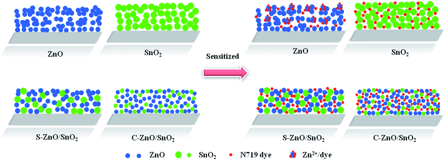
In order to explain the performance differences clearly, a model of the photoanode film structure without and with dye loading has been drawn according to the SEM images, BET analysis and UV-vis absorption and is shown in Fig. 8.
 |
| | Fig. 8 Model of the photoanode film structure without and with dye loading. | |
In Fig. 3, the particle agglomeration was very significant in the ZnO photoanode film, so in the model it was drawn in this way. Meanwhile, some studies have proven that ZnO would dissolve into a N719 dye bath, and that surface aggregation would occur between Zn2+ and the dye (Zn2+/dye).23,24 For the ZnO photoanode film, it can be speculated that the film structure and semiconductor properties of ZnO might be destroyed after 12 h immersing (shown in Fig. 8), so that Cell 1 would have a lower PCE. Owing to the bigger particles and pores, a smaller surface area was obtained, so the dye adsorption capacity of the SnO2 photoanode film was very poor. In addition, thanks to the low conduction band that led to a low photovoltage and fast recombination rate,9,25 Cell 2 showed the lowest open-circuit voltage (Voc) of 0.42 V and a PCE of 0.89%. A typical characteristic of the S-ZnO/SnO2 film was that the nanoparticles with two kinds of size attached to each other to form a heterogeneous film structure with a bad interface combination strength, as shown in Fig. 8. The C-ZnO/SnO2 photoanode film showed a uniform film structure, the largest BET surface area, dye loading and the best interface combination strength, which were all helpful to improve the performance of the DSSCs, so the PCE of Cell 4 was the best with 5.36%.
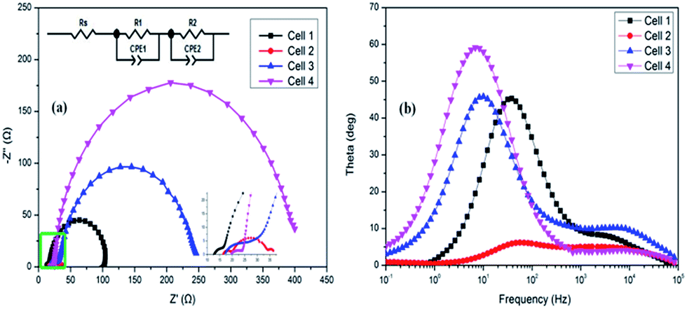
Analysis of electrochemical impedance spectroscopy (EIS)
The typical electrochemical impedance spectroscopy (EIS) Nyquist plots of the above four kinds of cells were studied to investigate the electron transfer at the interfaces of the photoanode film/dye/electrolyte within the frequency region of 0.1–100000 Hz. The EIS spectra are shown in Fig. 9a, the equivalent circuit model of the device and partial enlarged view (green square) are inserted. The arc in the high frequency region showed the electron transfer resistance based on the electrolyte/Pt electrode interface, and the larger arc in the low frequency region represented the recombination of electrons at the photoanode film/dye/electrolyte interface.27,32,33
 |
| | Fig. 9 EIS spectra of the different cells: (a) Nyquist plot; (b) Bode plot. | |
According to the equivalent circuit model, all of the cells have a similar Rs and a close R1 for the same Pt electrode. The R2 told of an easier electron recombination process for the corresponding photoanode, and the R2 follow the order of C-ZnO/SnO2 < S-ZnO/SnO2 < ZnO < SnO2 (as shown in Table 2). Two reasons can be used to explain the lower R2 value of Cell 4: the C-ZnO/SnO2 composite structure offered a better electron transferring channel and a larger surface area with better dye loading resulted in a larger recombination resistance.
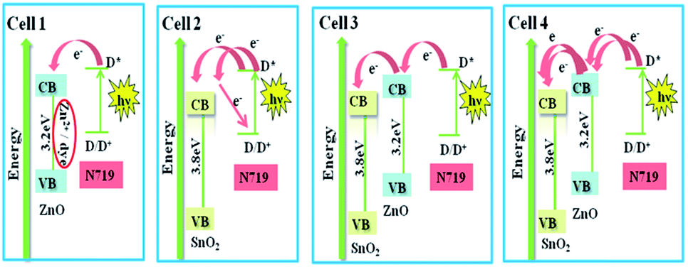
What’s more, the method of charge transfer was also different for the cells. For Cell 1, by virtue of the Zn2+/dye aggregation, the film structure and electronic transmission channel had been destroyed, resulting in a poor performance. Due to the low conduction band in SnO2, which led to a failing electron-injection and fast recombination rate, the carrier concentration and utilization decreased for Cell 2. In the composite structure of S-ZnO/SnO2 and C-ZnO/SnO2, first, the excited electrons were injected into the conduction band of ZnO, and then transfused into the conduction band of SnO2, which would ensure more electrons be collected and a lower recombination. Cell 4 was assembled with the C-ZnO/SnO2 photoanode, which had a larger surface area and dye loading, so more carriers have been showed compared with Cell 3. The simulation of electron transfer in the cells is shown in Fig. 10.34
 |
| | Fig. 10 Simulation of electron transfer. | |
The Bode plot is shown in Fig. 9b to investigate the electron lifetime (τe) of the different cells. The electron lifetime was measured using the following relationship, and the corresponding parameters are shown in Table 2.
where
τe is the electron lifetime, and
f is the frequency of peak.
It was obvious that the τe decreased in the following sequence: C-ZnO/SnO2 > S-ZnO/SnO2 > ZnO > SnO2, which indicated a high-usage of electrons might happen in Cell 4. The EIS results demonstrated that electrons with a lower recombination rate, faster transport and longer lifetime had a positive effect and enhanced the device performance in Cell 4.
Conclusion
Four kinds of photoanodes were fabricated for DSSCs, including ZnO, SnO2, simple mixed ZnO/SnO2 (S-ZnO/SnO2) and complex composite ZnO/SnO2 (C-ZnO/SnO2) using a two-step solid state reaction method (first a low heat solid state reaction and next mild sintering). It is the first time to prepare DSSC photoanode materials using this effective method. The results demonstrate that the C-ZnO/SnO2 photoanode has a larger BET surface area, the best dye-loading ability and a better inhibition of electron–hole recombination. As a result, the DSSC based on the C-ZnO/SnO2 photoanode shows the highest photoelectric conversion efficiency of 5.36%, compared with ZnO, SnO2 and S-ZnO/SnO2. At the same time, the composite photoanode successfully enhances the chemical stability of the device under acidic conditions when immersed for a long time.
Notes and references
- B. O’Regan and M. Grätzel, Nature, 1991, 353, 737–740 CrossRef.
- K. Zhu, N. R. Neale, A. Miedaner and A. J. Frank, Nano Lett., 2007, 7, 69–74 CrossRef CAS PubMed.
- F. F. Santiago, J. Bisquert, G. G. Belmonte, G. Boschloo and A. Hagfeldt, Sol. Energy Mater. Sol. Cells, 2005, 87, 117–131 CrossRef.
- C. Liu, Z. Liu, E. Lei, Y. Li, J. Han, Y. Wang, Z. Liu, J. Ya and X. Chen, Electron. Mater. Lett., 2012, 8, 481–484 CrossRef CAS.
- S. Mathew, A. Yella, P. Gao, R. Humphry-Baker, B. F. E. Curchod, N. Ashari-Astani, I. Tavernelli, U. Rothlisberger, M. K. Nazeeruddin and M. Grätzel, Nat. Chem., 2014, 6, 242–247 CrossRef CAS PubMed.
- Z. Liu, Y. Li, C. Liu, J. Ya, E. Lei, W. Zhao, D. Zhao and L. An, ACS Appl. Mater. Interfaces, 2011, 3, 1721–1725 Search PubMed.
- S. Ameen, M. S. Akhtar, H.-K. Seo, Y. S. Kim and H. S. Shin, Chem. Eng. J., 2012, 187, 351–356 CrossRef CAS.
- Z. Liu, J. Han, K. Guo, X. Zhang and T. Hong, Chem. Commun., 2015, 51, 2597–2600 RSC.
- J. Chen, C. Li, F. Xu, Y. Zhou, W. Lei, L. Sun and Y. Zhang, RSC Adv., 2012, 2, 7384–7387 RSC.
- S. Gubbala, V. Chakrapani, V. Kumar and M. K. Sunkara, Adv. Funct. Mater., 2008, 18, 2411–2418 CrossRef CAS.
- N. Jeon and D. W. Kim, J. Nanosci. Nanotechnol., 2013, 13, 7955–7958 CrossRef CAS PubMed.
- J. Kim and J. Kim, J. Nanosci. Nanotechnol., 2011, 11, 7335–7338 CrossRef CAS PubMed.
- X. Jin, C. Liu, J. Xu, Q. Wang and D. Chen, RSC Adv., 2014, 4, 35546–35553 RSC.
- I. Hod, M. Shalom, Z. Tachan, S. Rühle and A. Zaban, J. Phys. Chem. C, 2010, 114, 10015–10018 CrossRef CAS.
- T. Lana-Villarreal, G. Boschloo and A. Hagfeldt, J. Phys. Chem. C, 2007, 111, 5549–5556 CrossRef CAS.
- K. Wang, Y. T. Shi, W. Guo, X. Q. Yu and T. L. Ma, Electrochim. Acta, 2014, 135, 242–248 CrossRef CAS.
- K. Prabakar, M. Son, W. Y. Kim and H. Kim, Mater. Chem. Phys., 2011, 125, 12–14 CrossRef CAS.
- Q. Zhang, C. S. Dandeneau, X. Zhou and G. Cao, Adv. Mater., 2009, 21, 4087–4108 CrossRef CAS.
- Z. Dong, X. Lai, J. E. Halpert, N. Yang, L. Yi, J. Zhai, D. Wang, Z. Tang and L. Jiang, Adv. Mater., 2012, 24, 1046–1049 CrossRef CAS PubMed.
- Y. F. Tu, Q. M. Fu, X. J. Niu, J. P. Sang, Z. J. Tan, G. Zheng and X. W. Zou, Cryst. Res. Technol., 2013, 48, 138–144 CrossRef CAS.
- X. Kang, C. Jia, Z. Wan, J. Zhuang and J. Feng, RSC Adv., 2015, 5, 16678–16683 RSC.
- Y. Chergui, N. Nehaoua and D. E. Mekki, Comparative Study of Dye-Sensitized Solar Cell Based on ZnO and TiO2 Nanostructures, INTECH Open Access Publisher, 2011 Search PubMed.
- K. Keis, C. Bauer, G. Boschloo, A. Hagfeldt, K. Westermark, H. Rensmo and H. Siegbahn, J. Photochem. Photobiol., A, 2002, 148, 57–64 CrossRef CAS.
- R. Schölin, M. Quintana, E. M. J. Johansson, M. Hahlin, T. Marinado, A. Hagfeldt and H. Rensmo, J. Phys. Chem. C, 2011, 115, 19274–19279 CrossRef.
- A. N. M. Green, E. Palomares, S. A. Haque, J. M. Kroom and J. R. Durrant, J. Phys. Chem. B, 2005, 109, 12525–12533 CrossRef CAS PubMed.
- W. Chen, Y. Qiu, Y. Zhong, K. S. Wong and S. Yang, J. Phys. Chem. A, 2009, 114, 3127–3138 CrossRef PubMed.
- Y. Zhou, C. Xia, X. Hu, W. Huang, A. A. Aref, B. Wang, Z. Liu, Y. Sun, W. Zhou and Y. Tang, Appl. Surf. Sci., 2014, 292, 111–116 CrossRef CAS.
- J. Liu, Y. Gu, Z. Qin and Y. Zhang, Int. Conf. Mater. Renewable Energy Environ., 2014, 1, 66–69 Search PubMed.
- S. Ito, Y. Makari, T. Kitamura, Y. Wada and S. Yanaqida, J. Mater. Chem., 2004, 14, 385–390 RSC.
- N. K. Huu, D. Y. Son, I. H. Jang, C. R. Lee and N. G. Park, ACS Appl. Mater. Interfaces, 2013, 5, 1038–1043 Search PubMed.
- K. H. Ko, Y. C. Lee and Y. J. Jung, J. Colloid Interface Sci., 2005, 283, 482–487 CrossRef CAS PubMed.
- X. Dou, D. Sabba, N. Mathews, L. H. Wong, Y. M. Lam and S. Mhaisalkar, Chem. Mater., 2011, 23, 3938–3945 CrossRef CAS.
- P. Tiwana, P. Docampo, M. B. Johnston, H. J. Snaith and L. M. Herz, ACS Nano, 2011, 5, 5158–5166 CrossRef CAS PubMed.
- J. Han, Z. Liu, K. Guo, J. Ya, Y. Zhao, X. Zhang, T. Hong and J. Liu, ACS Appl. Mater. Interfaces, 2014, 6, 17119–17125 Search PubMed.
|
| This journal is © The Royal Society of Chemistry 2015 |
Click here to see how this site uses Cookies. View our privacy policy here.