
 Open Access Article
 This Open Access Article is licensed under a
 Creative Commons Attribution 3.0 Unported Licence
Dynamic synergy of tin in the electron-transfer layer and absorber layer for advancing perovskite solar cells: a comprehensive review
Azaharuddin Saleem
Shaikh
 a,
Subhash Chand
Yadav
a,
Abhishek
Srivastava
a,
Archana R.
Kanwade
a,
Manish Kumar
Tiwari
a,
Shraddha Manohar
Rajore
a,
Jena Akash Kumar
Satrughna
b,
Mahesh
Dhonde
c and
Parasharam M.
Shirage
*a
a,
Subhash Chand
Yadav
a,
Abhishek
Srivastava
a,
Archana R.
Kanwade
a,
Manish Kumar
Tiwari
a,
Shraddha Manohar
Rajore
a,
Jena Akash Kumar
Satrughna
b,
Mahesh
Dhonde
c and
Parasharam M.
Shirage
*a
aDepartment of Metallurgical Engineering and Materials Science, Indian Institute of Technology Indore, Simrol, Khandwa Road, Indore 453552, India. E-mail: pmshirage@iiti.ac.in; paras.shirage@gmail.com
bDepartment of Physics, Indian Institute of Technology Indore, Simrol, Khandwa Road, Indore 453552, India
cDepartment of Physics, Medi-Caps University, Pigdamber, Rau, Indore, Madhya Pradesh 453331, India
First published on 23rd May 2024
Abstract
The landscape of metal halide-perovskite solar cells (MH-PSCs) has witnessed significant progress in terms of efficiency over the past decade. Nevertheless, concerns over the toxicity of lead (Pb)-based perovskite structures have restrained their full market potential. In response, the exploration of Sn perovskites has emerged as a promising alternative, fueled by their narrow band gaps, superior carrier mobilities, low-temperature production, economic viability, and reduced hysteresis. These Sn perovskites exhibit competitive PCE while addressing the toxicity issues of Pb-based PSCs. This comprehensive review delves into the pivotal role of Sn in advancing PSCs, offering a consolidated understanding of its multifaceted applications. The report extensively examines the incorporation of Sn-based electron-transfer layers (ETLs) and absorber layers within PSCs, encompassing various dimensions, such as synthesis techniques, optoelectrical features, the future of Pb-free solar cells, integration into double PSCs, and the impact of doping strategies. Finally, this review proposes the future perspectives and investigations needed to make Sn-based PSCs a viable alternative to Pb-based MH-PSCs.
1. Introduction
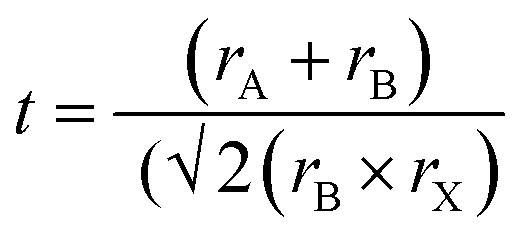
Renowned for their extraordinary potential in solar cells, metal halide perovskite semiconductors have emerged as propitious materials for solar cells, attracting considerable attention since 2009. Over the past few years, the efficiency of PSCs has impressively increased from 3.8% to 26.1%,1 rivalling the advances seen in thin-film solar cells and silicon solar cells. Leading perovskite materials, such as MAPbI3, FAPbI3, and mixed-cation perovskites, have emerged as candidates for high-performance solar devices.2 However, the toxicity associated with lead-based PSCs poses a significant challenge in their widespread adoption and commercial application.3Addressing this concern, the search for alternative environmentally friendly elements to replace Pb in PSCs has gained importance.4 Suitable metal elements should be able to produce a stable perovskite crystal structure; typically exhibiting an ABX3 structure, where A is a monovalent organic or inorganic cation, B is a coordinate divalent metal ion, and X can be any halogen like Cl−, Br−, or I−.5 To obtain a stable perovskite structure, precise ionic radii (r) of A, B, and X ions are essential, as determined by the tolerance factor:6,7
In 2014, Snaith et al. pioneered the utilization of MASnI3 as a light-absorbing material in PSCs, yielding a remarkably promising power conversion efficiency (PCE) of 6.4% within a mesoporous structure.14 This ground-breaking achievement has since sparked substantial interest in Sn perovskites, fuelling extensive research to attain high-performance Sn-based PSCs. Indeed, Sn-based PSCs have received considerable research attention, approximating to the efforts that boosted Pb-based perovskites. Despite their low PCEs and vulnerability of Sn to oxygen and moisture in the ambient atmosphere, which can lead to structural transitions and difficulty in creating pinhole-free films, extensive research has been done globally to develop Sn-based PSCs as an alternative to Pb-based PSCs. Notably, CsSnI3, CH3NH3SnI3 (MASnI3), and (NH2)2CHSnl3 (FASnI3) have been prevalently used in PSCs, and the best-reported PCEs for these devices have reached approximately 7.5%, 12.5%, and 14.1%, respectively,15 indicating high performance even with reduced or Pb-free Sn-based perovskites. The ongoing work in tin-based perovskite research promises to lead the way toward safer, more efficient, and eco-friendly solar cell technologies, thereby contributing significantly to the sustainable development of renewable energy.
Apart from its usage in Pb-free PSCs, Sn oxide (SnO2) has emerged as a preferable choice for the ETL in PSCs, gaining significant attention due to its various advantages,16 including: (i) SnO2 possesses an acute conduction band (CB) with favourable energy levels and band alignments. The ETL–perovskite interface actively enhances the extraction of electrons and effectively prevents the movement of holes. Also, it may help to reduce interfacial strain (by reducing the lattice mismatch) induced during the synthesis process; (ii) SnO2 possesses a wide optical bandgap (∼3.6 eV), which can block UV-light infiltration while allowing excellent transparency throughout the visible range. As a result, a significant portion of light can effectively infiltrate and be assimilated by the perovskite film; (iii) SnO2 displays remarkable bulk electron mobility, reaching 240 cm2 V−1 s−1, coupled with exceptional conductivity (∼7.5 × 10⁻⁶ S cm−1). These characteristics promise to improve electron transport effectively while reducing recombination disadvantages; (iv) SnO2 demonstrates remarkable chemical stability, resistance to UV-light filtration, and reduced photocatalytic activity compared to materials like titanium dioxide (TiO2) and other ETLs, which are critical for maintaining devices’ overall stability and reliability; and (v) SnO2 is ideally suited to low-temperature processing (<200 °C), making it ideal for flexible solar cells, tandem solar cells, and a wide range of commercial perspectives.
Herein, we comprehensively present an overview of the recent progress, remaining challenges, and future perspectives concerning the potential applications of Sn-based ETLs and absorber layers to be utilized in Pb-free PSCs. The review begins by describing and discussing the various synthesis procedures aimed at making high-quality Sn-based perovskite films, focusing on their impact on the performance and operational stability of PSCs. In addition, a comprehensive assessment of the structural, electrical–optical, and modification methodologies, as well as current breakthroughs in SnO2-type ETLs and their significance in PSCs, are discussed. Further, this review thoroughly explores the emerging field of Sn-based perovskites in solar cell applications. In contrast to the prevailing focus on metal halide perovskite semiconductors, it uniquely emphasizes the potential of Sn as a promising lead-free alternative. This review meticulously examines the intricacies, offering a comprehensive understanding of the challenges and opportunities for replacing Pb with environmentally friendly elements. Notably, it goes beyond Sn perovskites’ light-absorbing properties to discuss their application as an ETL, strategically highlighting the advantages of SnO2 in this area. This dual focus, addressing Sn perovskites as both ETLs and absorber layers, provides a holistic perspective on the potential application of Sn perovskites in solar cell technologies. The article's distinctive approach, seamlessly integrating historical perspectives, material properties, synthesis approaches, and potential applications, positions it as a valuable resource for potential readers exploring the evolving landscape of Pb-free PSCs.
2. Role of Sn in the ETL
In recent years, there has been an increasing interest in employing SnO2 as an ETL in PSCs. Despite the initial challenges faced by SnO2 in organic solar cells and dye-sensitized solar cells compared to zinc oxide (ZnO) and TiO2, the landscape shifted significantly in 2015, when several research groups independently introduced SnO2 into PSCs and reported notable improvements in device efficiency. For example, Ma et al. and Kuang et al. reported efficiencies of 7.43% and 14.69%, respectively.17,18 Despite these advancements, challenges related to charge traps and recombination centres, such as oxygen vacancies resulting from high-temperature annealing at 450 °C, were initially encountered in SnO2-based PSCs. To address these issues, researchers developed low-temperature processing methods for SnO2. For instance, Tian et al. achieved a PCE of 13% by spin-coating SnO2 nanoparticles and annealing at 200 °C.19 Fang et al. reported a noteworthy 17.21% efficiency using a low-temperature thermal decomposition process at 180 °C.20 Additionally, Hagfeldt and colleagues employed a low-temperature atomic layer deposition (ALD) approach, achieving a PCE of over 18% with the open-circuit voltage (Voc) exceeding 1.19 V.21Building on these findings, recent breakthroughs by You's group22 demonstrated a certified efficiency of 19.9%, utilizing high-quality SnO2 nanocrystal colloids annealed at a moderate temperature of 150 °C. Recent developments, including meticulous control of the surface passivation layers and interface modifications, have propelled SnO2-based PSCs to efficiencies surpassing 21.6%.23–26 Moreover, the competitiveness of SnO2 with TiO2 in terms of performance is underscored by recent studies. Noteworthy achievements include planar PSC architectures with PCEs exceeding 21% and exceptional stability, retaining 82% of the original PCE after 60 h of use. Other configurations, such as SnO2/PCBM composites and SnO2 alloyed with c-TiO2, have reported PCE values surpassing 19%.27,28 The favourable optoelectronic properties of SnO2 make it a compelling candidate for the ETL in PSCs.29–32 Low-temperature processed SnO2 has demonstrated great promise, showing a PCE of 13% with high stability. Chemical treatments and surface modifications, including elemental doping, surface passivation, and bilayer structures, have further elevated the performance of SnO2-based PSCs.20,33–35 The evolving role of SnO2 as an ETL in PSCs reflects the substantial progress in the use of SnO2, with recent accomplishments showcasing its potential to compete with TiO2-based devices. Ongoing research endeavours are aiming to refine SnO2-based PSCs through innovative approaches, setting the stage for improving the efficiency and stability of next-generation solar cell technologies.
2.1. Synthesis methods for SnO2
Various synthesis techniques are utilized for SnO2 thin films, including sol–gel, hydrothermal, sonochemical, microwave-assisted, ALD, chemical vapour deposition (CVD), and sputtering techniques. The sol–gel method involves converting a precursor sol into a solid gel, offering good film thickness and composition control. Hydrothermal synthesis uses high-pressure and high-temperature conditions to promote film growth with improved crystallinity. Sonochemical and microwave-assisted methods utilize ultrasonic or microwave irradiation to enhance the nucleation and crystallization processes. ALD enables a precise and conformal film deposition, while CVD allows large-scale production. Sputtering offers excellent uniformity and composition control. Understanding the characteristics and experimental conditions of each method is vital for tailoring SnO2 films to specific applications.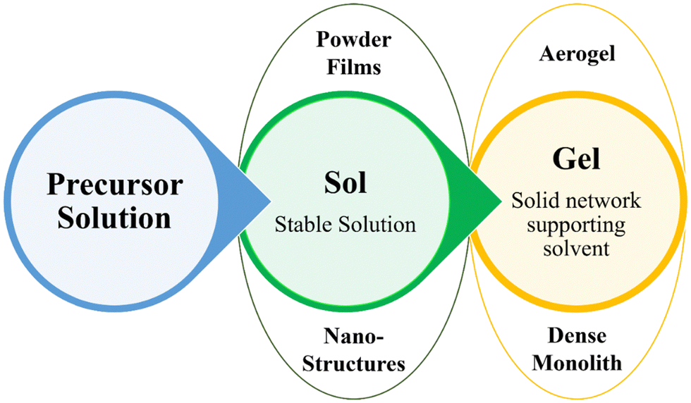 | ||
| Fig. 1 Graphical overview of the sol–gel method and its potential applications. | ||
In materials synthesis, gelation typically involves the irreversible establishment of covalent bonds. When the solution experiences gelation, it culminates in creating unified materials. These gel frameworks can undergo additional treatment through meticulous dehydration and heating, fabricating top-notch ceramic or glass structures. Alternatively, supercritical solvent extraction permits highly porous and lightweight unified forms. Gelation can also occur during various processing stages, frequently via the evaporation of solvents, which yields valuable materials. For instance, films created through spinning or dipping encounter gelation during the drying phase and can subsequently be subjected to heating to generate compact films. Spherical particles can be produced by spray drying, while fibres may emerge through spinning accompanied by evaporation. Furthermore, the introduction of templating agents enables the utilization of gelation to fashion nanoporous materials and other nanostructures, like tubes, fibres, helices, and ribbons.40–43
Films of SnO2 were generated through a spin-coating technique, involving the application of SnO2 organic sol onto pristine substrates at 5000 rpm for 30 s, followed by sintering at 450 °C for 2 h. The SnO2 organic sol was derived by dissolving SnCl2·2H2O in absolute ethyl alcohol, stirring at 80 °C for 3 h, ageing, and subsequently employing it to coat the films at different concentrations. The optimal concentration was found to be 0.5 M.44 The SnO2 ETLs were formed through a solution-based spin-coating technique using SnCl2·2H2O precursor solution, followed by thermal annealing at 180 °C for 1 h and UV-ozone treatment. This low-temperature process yielded excellent SnO2 ETLs, resulting in efficient PSCs. Also, the method is compatible with low-cost, roll-to-roll manufacturing on flexible substrates.45 In a separate investigation, SnO2 nanoparticles were fabricated through a process involving the reaction of SnCl4·5H2O and aqueous TMAH in ethanol. Ultrasonic treatment was then applied, followed by hydrothermal synthesis at 200 °C for 12 h. The outcome was the formation of layers of SnO2 through spin-coating a precursor solution at 2000 rpm, leading to the development of layers with an approximate thickness of 120 nm. This layer of SnO2 could serve as an effective material for transporting electrons in PSCs. The cells achieved an impressive PCE of 18.8%. Notably, even after being stored under standard environmental conditions for 30 days, the SnO2 layer maintained its initial PCE at a level exceeding 90%. This underscores the improved stability of the SnO2 layer.46 Using a different approach, a colloidal solution of SnO2 quantum dots (QD) was created, resulting in a substantial increase in the PSC of 20.1%. This advancement was due to the remarkable optical and electronic characteristics of the ETL based on SnO2 QDs. Experimental assessment illustrated the elevated efficiency of solar cells with this material due to the augmentation of electron extraction and mitigation of charge recombination. The most suitable solution concentrations and ratios for optimal efficacy were also determined.47
Gu et al. successfully prepared SnO2 nanopowders through a hydrous Sn chloride dissolution method, followed by the controlled dropwise addition of 2 M aqueous ammonia solution. The SnO2 nanopowders exhibited a quantum confinement effect, leading to a higher energy absorption edge as the particle size decreased. Samples treated at different temperatures showed varying absorption positions, indicating direct electron transitions in the SnO2 nanocrystals.48 Also, in the work of Adnan et al., a sol–gel synthesis of SnO2 nanoparticles involved mixing Sn(IV) chloride with water, then gradually adding ammonia solution and stirring for 2 h before ageing the solution. The gel obtained was rinsed, dried, and subjected to calcination at 400 °C. This simple method resulted in the creation of nanoparticles of SnO2 showcasing a significant surface area.49 Zhang et al. employed a sol–gel method to synthesize SnO2 nanoparticles by adding 8 mol L−1 of HNO3 to a granulated Sn and citric acid mixture. This addition stabilized the precursor solution, resulting in smaller, evenly shaped SnO2 particles after calcination at different temperatures. The study highlighted the potential of this straightforward approach for controlling the production of SnO2 nanoparticles with desirable properties.50 Aziz et al. used a process involving dissolving hydrated Sn chloride in pure ethanol and stirring for 30 min, followed by adding acetylacetone to initiate the hydrolysis of SnO2. The solution was refluxed at 80 °C for 5 h to form the SnO2 solution. The researchers introduced polyethylene glycol (PEG) as a chemical modifier to control the nanoparticle size and aged the solution for 72 h. Subsequently, the solution was dried at 100 °C for 30 min and subjected to calcination at 450 °C and 600 °C for 1 h, forming SnO2 nanoparticles. By adjusting the calcination temperature and the molecular weight of the PEG, the nanoparticle size could be precisely controlled. This method is a solid foundation for future studies focusing on synthesizing metal oxide nanoparticles with a controlled size and shape, paving the way for various applications in various fields.51Table 1 summarizes the synthetic conditions and improved results obtained with sol–gel methods in some studies.
| Precursors | Synthesis conditions | Result | Ref. |
|---|---|---|---|
| SnCl2·2H2O and ethyl alcohol | Sol temp.: 80 °C | Minimized the occurrence of a charge shunt pathway | 44 |
| Stirring: 3 h | |||
| Ageing: 3 h | |||
| SnCl2·2H2O and ethyl alcohol | Sol temp.: 80 °C | Surface becomes uniform, hence having a positive impact on light transmission | 45 |
| Annealing temp.: 180 °C for 1 h | |||
| SnCl4·5H2O and TMAH in ethanol | Sol temp.: 100 °C for 12 h | High degree of crystallinity, effective electron transfer, and enhancement in the stability of the devices against oxygen and water | 46 |
| SnCl2·2H2O and CH4N2S in deionized water | Sol temp.: RT | 97% transmission in visible light | 52 |
| Ageing: 2 days | |||
| SnCl4·5H2O and ammonia solution | Sol temp.: 80 °C | Increased absorption edge energy due to the quantum confinement effect | 48 |
| Annealing temp.: 400 °C, 500 °C, and 600 °C for 2 h | |||
| SnCl4·5H2O and ammonia solution | Sol temp.: 30 °C to 90 °C | Formation of numerous small nuclei results in a larger sample surface area | 49 |
| Stirring: 2 h | |||
| Ageing: 24 h | |||
| Calcination: 400 °C for 2 h | |||
| Granulated tin, citric acid, nitric acid, aqueous ammonia | Sol temp.: 100 °C | Reduction in particle size | 50 |
| Drying: 100 °C for 5 h in air | |||
| Calcination: 300 °C for 2 h, 400 °C for 2 h, 500 °C for 2 h | |||
| SnCl2·2H2O and ethyl alcohol, acetylacetone, PEG | Sol temp.: 80 °C for 5 h | Control over the size of particles | 51 |
| Ageing: 72 h | |||
| Drying: 100 °C for 0.5 h | |||
| Calcination: 450 °C for 1 h and 600 °C for 1 h |
Table 2 compares devices utilizing SnO2 layers as the ETL, synthesized through the sol–gel method. The FTO/SnO2/MAPbI3/spiro-OMeTAD/Au configuration seems to be the most favourable option, with a higher Voc, improved FF, and superior PCE compared to the FTO/SnO2-ESL/perovskite/HTM/Ag structure. However, the latter configuration exhibited a higher Jsc, indicating efficient light absorption and carrier generation. Further optimization efforts could focus on enhancing the FF and overall device performance of both structures. These discoveries emphasize the importance of carefully selecting materials and designing device structures when aiming for higher performance in PSCs. Ongoing exploration and progress in this domain are needed for enhancing the effectiveness and economic feasibility of these technologies within the realm of renewable energy applications.
| Device structure | V oc [V] | J sc [mA cm−2] | FF [%] | PCE [%] | Ref. |
|---|---|---|---|---|---|
| FTO/SnO2-ESL/MAPbI3/HTM/Ag | 0.86 | 30.99 | 0.39 | 10.33 | 44 |
| FTO/SnO2/MAPbI3/spiro-OMeTAD/Au | 1.11 | 22.83 | 0.64 | 16.02 | 45 |
| FTO/NiO/MAPbI3/C60/SnO2NCs/Ag | 1.12 | 21.8 | 0.77 | 18.8 | 47 |
| ITO/P3CTK/MAPbI3/PC61BM:SnO2/Al | 1.12 | 23.13 | 0.72 | 18.7 | 53 |
| ITO/PEN/SnO2QD-ESL/CsMAFA/spiro-OMeTAD/Au | 1.12 | 23.55 | 0.78 | 20.3 | 52 |
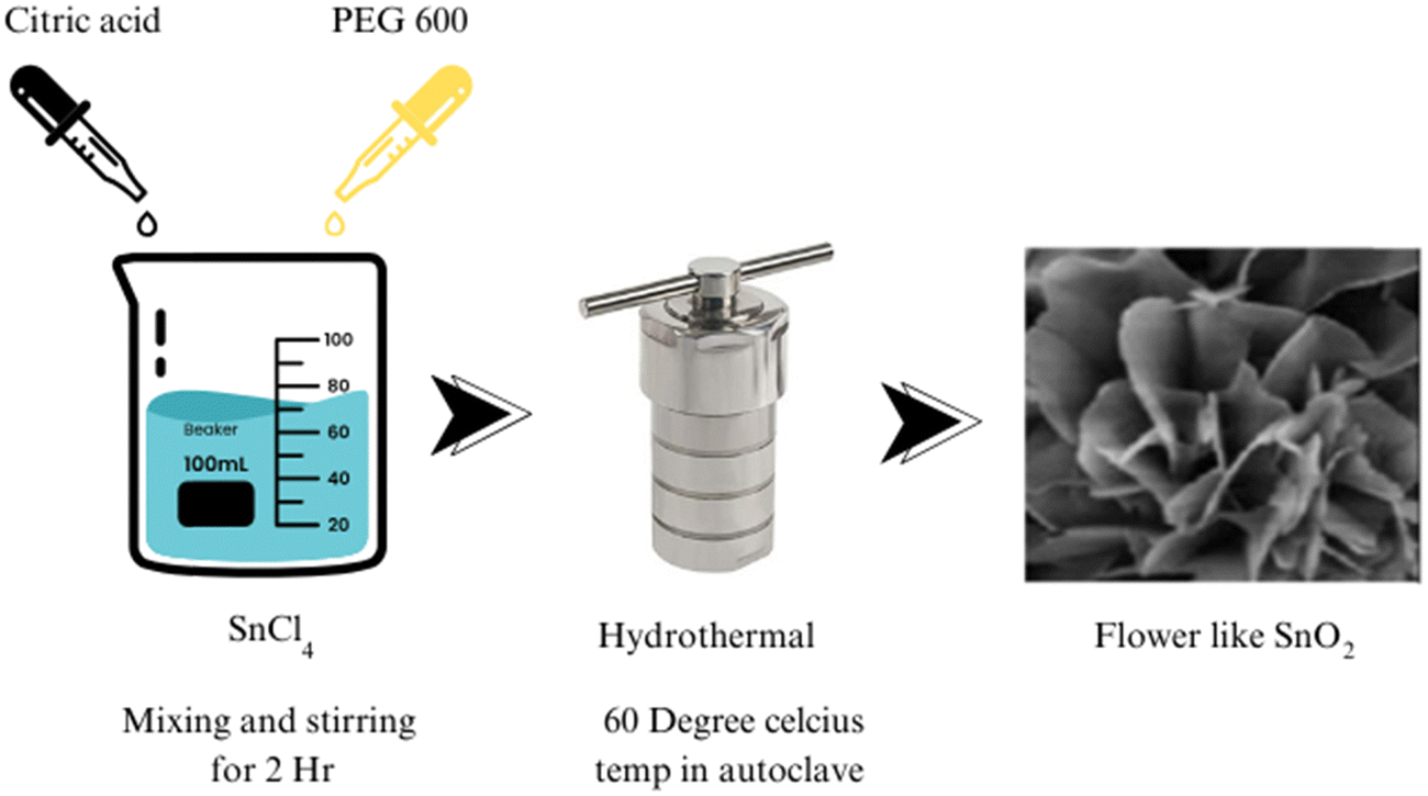 | ||
| Fig. 2 Synthesis of a flower-like morphology of SnO2 using the hydrothermal method. | ||
| Reaction temp. (°C) | Reaction time (h) | Basic reagents | Morphology | Ref. |
|---|---|---|---|---|
| 240 | 15 | SnCl4·5H2O, lysine | Nanoparticles | 57 |
| 250 | 24 | SnCl4·5H2O, CTAB, Triton X-100, sodium hydroxide, sodium dodecyl sulphate | Nanoparticles | 58 |
| 200 | 18 | Urea, SnCl2·2H2O, NaOH | 3D nano spheres | 59 |
| 140 | 16 | SnCl, NH3, NaOH | Nanorods | 60 |
| 140 | 24 | SnCl4·5H2O, NaOH, CTAB | Nanosheets | 61 |
| 150 | 24 | SnCl4·5H2O | Nanorods | 62 |
The hydrothermal method, leveraging its unique capacity to engineer SnO2 thin films with tailored properties, presents a promising avenue for a wide range of applications, encompassing sensing devices and energy-storage systems. By harnessing the advantages offered by hydrothermal synthesis, researchers can forge ahead in developing SnO2 thin films characterized by enhanced functionality and performance, thereby contributing to significant advancements across various technological domains.63
Significant advancements in SnO2 synthesis have been achieved using the hydrothermal method. Through a hydrolysis reaction, ultrathin single-crystalline nanorods of SnO2 were synthesized by Ye et al., showcasing a nonclassical crystallization process. Zeng et al. successfully fabricated hierarchical flower-like SnO2 architectures using a hydrothermal route, as shown in Fig. 2, with the assistance of solid citrate and PEG 600, elucidating the role of chelate complex formation and soft templates. Cheng et al.62 created SnO2 nanorods with a preferred (001) growth direction and high aspect ratio. Hussain et al. achieved the catalyst-free growth of SnO2 micro-sheets, with the thickness increasing as the reaction temperature rose.64 Guo et al. demonstrated the fabrication of hierarchical SnO2 nanostructures using shuttle-shaped nanosheets that transformed into cone-shaped and rod-shaped structures under thermal treatment.65 Wang et al. reported controlling the size and morphology of SnO2 nanoparticles through solution adjustments.66 A novel biomolecule-assisted hydrothermal method for synthesizing sub-10 nm SnO2 nanocrystals with exceptional photocatalytic performance, addressing significant challenges in nanoparticle synthesis and offering a highly efficient approach for organic dye degradation.67 Yin et al. investigated the influence of the reaction conditions on the SnO2 nanocrystal morphology using L-lysine.68 Wang et al. investigated a hydrothermal method to obtain nanoflowers of SnO2 at a large scale.69 Zhang et al. developed a simplistic method for SnO2 microsphere synthesis.70 Lou et al. reported the synthesis of hierarchical SnO2 structures from nanosheets.71 Maksimov et al. obtained SnO2 nanocrystals with diverse morphologies via a hydrothermal synthesis.72 Talebian et al. explored the role of surfactants in controlling the morphology of SnO2.73 Lee et al. utilized a solvothermal synthesis to create a hollow core–shell mesosphere composed of SnO2 nanoparticles.74
Uniform distribution over large areas can be achieved by CVD, ensuring a consistent deposition of the desired material, which is particularly beneficial when homogeneity across the substrate is essential. Additionally, CVD enables the deposition of materials without compositional gradients, ensuring uniformity throughout the deposited layer.75–77 The CVD procedure utilizes a heated furnace that can attain elevated temperatures, a critical factor facilitating effective reactions and/or the breakdown of volatile precursor materials on the substrate's surface, which culminates in the desired formation of deposits. A pressure sensor is integrated into the system to ensure precise control and monitoring during the CVD process. This sensor helps maintain the optimal pressure conditions within the furnace, essential for achieving a consistent and uniform deposition of the desired material. In the CVD set-up, the substrate, typically a wafer, is vertically placed to facilitate the deposition process. This vertical orientation allows for better substrate exposure to the volatile precursors, improving deposition efficiency and uniformity. The process may involve the liberation of gases during the chemical reactions, and so a vacuum pump is employed to manage these gases and maintain controlled conditions. The vacuum pump helps create and sustain the required vacuum environment within the furnace, which is necessary for the CVD process to proceed effectively.63,78,79 The overall set-up and components of the CVD process, including the heated furnace, pressure sensor, vertically placed wafer for deposition, and vacuum pump, are depicted in Fig. 3.
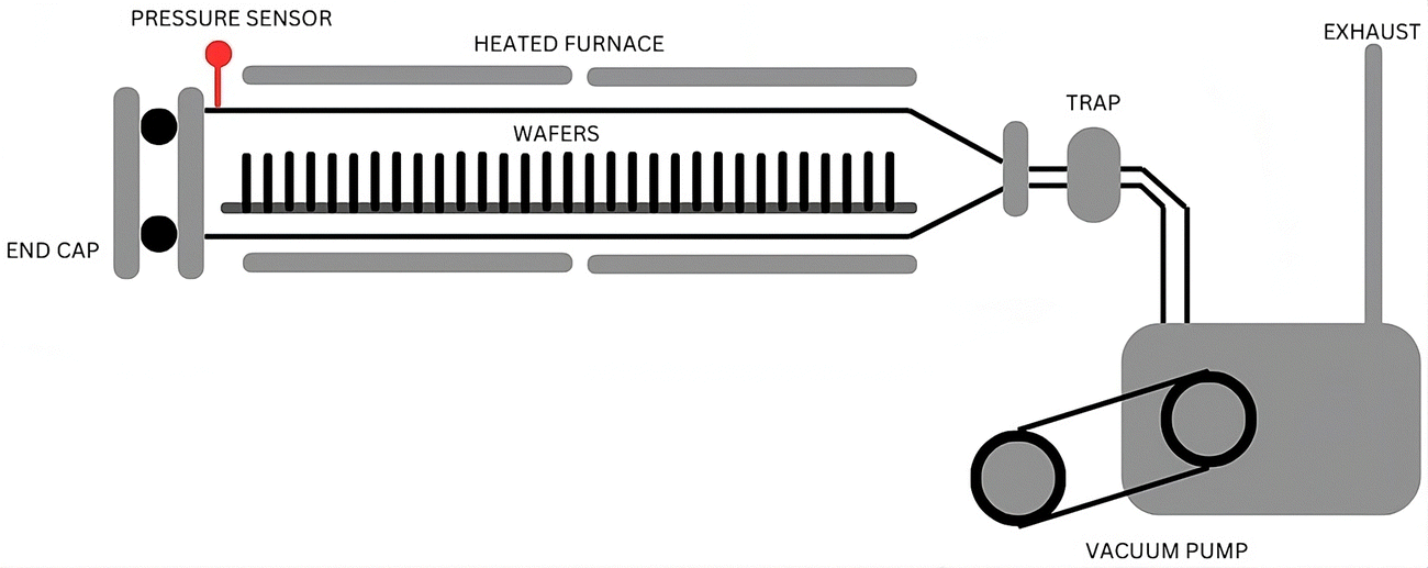 | ||
| Fig. 3 Schematic illustrating the chemical vapour deposition process. | ||
In synthesizing SnO2 nanostructures, CVD offers a simple and efficient technique. By evaporating targets, such as Sn, SnO, and SnO2, at varying temperatures, a wide range of SnO2 nanostructures can be prepared. Hierarchical nano-homojunctions and nano-heterojunctions were achieved with controlled growth by Sun et al.,80 using a multistep thermal vapour deposition route. On the exterior of the single-crystal SnO2 nanobelt bases, multiple aligned SnO2 nanowires or nanobelts were cultivated through a catalyst-free vapor–solid (VS) growth process. The successive development of nanowire or nanobelt levels allowed for a theoretically limitless structure complexity, with different lengths, sizes, and chemical compositions at each branch level. SnO2 nanostructures with various morphologies were synthesized by Ge et al.81 using a catalyser-assisted CVD method, and it was noted that the quality of the SnO2 nanowires could be considerably impacted by the temperature during growth, and as the growth temperature rose, the magnetization lessened. A correlation between magnetization, morphology, and surface-to-volume ratio was also observed, with an increasing trend of magnetization as the surface-to-volume ratio increased. Other authors, including Mathur et al.,82 Yang et al.,83 Manna et al.,84 Liu et al.,85 and Zhang et al.,86 demonstrated control over the morphology, size, and other properties of SnO2 nanostructures could be achieved by adjusting the synthesis conditions such as temperature, deposition time, flow rates, and precursor selection. Barth et al.87 employed a molecule-assisted and gold-catalysed CVD method to obtain aligned SnO2 nanowires using a single-molecular source [Sn-(OtBu)4]. The catalysing function of gold facilitated the advancement of SnO2 on a single-crystal rutile substrate. The Sn4+–O species released during precursor decomposition were especially alloyed with gold nanoparticles or diffused to energetically favoured nucleation sites, leading to a heteroepitaxy of SnO2 on TiO2. Table 4 presents the reaction conditions employed in the CVD method and details of the reagents used.
Using a mild ultrasonic method that was also rapid, facile, and efficient, Qurashi et al. successfully synthesized SnO2 nanoparticles at lower temperatures. Their process offered a simple and effective means to prepare SnO2 nanoparticles.95 Goswami et al. documented the development of hollow SnO2 nanostructures on cellulose acetate using a sonochemical spinning process. By subjecting an ethylene glycol solution of stannous chloride to microwave irradiation, then utilizing ultrasonication, they were able to create hollow SnO2 nanotubes with a notable surface roughness and porosity.96 Gedanken et al. utilized this method to prepare spherical SnO2 nanoparticles, employing a solution of SnCl4 and azodicarbonamide in water. The nanoparticles formed a porous irregular network structure. They also showed an increased particle size with heating, exhibiting rounded hexagonal shapes after sintering at 800 °C.97 Zhu et al. developed a method for fabricating SnO2 nanotubular materials from cotton fibres. Ultrasonic treatment of the cotton fibres in SnCl2 solution followed by calcination preserved the initial cotton morphology, resulting in nanotubular materials.98 Kundu et al. compared the properties, such as microstructural and structural properties, of biosynthesized SnO2 powder through a gel calcination method with those synthesized by sonochemical and sol–gel methods resulting in the formation of highly crystalline SnO2 nanoparticles.99Table 5 outlines the conditions used in the sonochemical method.
Microwave irradiation has gained significant attention due to its ability to expedite the synthesis process, allowing reactions to complete in just a few minutes. This rapid reaction time is a substantial advantage, as it not only saves time but also enhances the overall efficiency of the synthesis process. Microwave heating facilitates the avoidance of temperature and concentration gradients, thus ensuring a uniform environment for the nucleation of nanomaterials.103 One of the crucial benefits of microwave synthesis is its ability to suppress side reactions, resulting in an improved yield and reproducibility of the desired product. By precisely controlling the reaction conditions, microwave-assisted synthesis minimizes undesired by-products and facilitates the production of high-quality SnO2 nanoparticles. This characteristic makes microwave synthesis an essential consideration for developing greener synthesis methodologies. Moreover, microwave-assisted synthesis holds immense potential for advancing the field of nanotechnology by offering a more environmentally friendly approach for the synthesis of nanoparticles. The utilization of microwave irradiation reduces the energy consumption required for synthesis, contributing to sustainable practices. With the increasing global demand for green and sustainable technologies, microwave synthesis is poised to play an important role in the future of synthetic nanotechnology.63,104,105
Kar et al. achieved the rapid synthesis of SnO2 nanorods and nanoparticles using microwave irradiation, where the morphology could be meticulously controlled by changing the irradiation temperature and time. The use of microwave irradiation facilitated a uniform growth and homogeneous heating, producing small, refined, and discrete particles.106 Yoshida et al. improved the microwave-assisted method for synthesizing shape- and size-controlled SnO2 nanocrystals in ethanol–water solvents. Their approach significantly promoted uniform nucleation and shortened the synthesis time, leading to a narrow size distribution of SnO2 particles.107 Patra et al. prepared SnO2 nanoparticles utilizing oleylamine and a capping agent. The choice of capping agents played a crucial role in tuning the crystal growth and morphology, and a texturing effect was observed, indicating preferred directional growth.108 Aoyagi et al. synthesized single SnO2 crystals with different shapes (columnar crystals and silver grass-like nanowhiskers) through the careful microwave heating of a TiO2–SnO2 blend. The shape of the crystals was found to be strongly influenced by the atmosphere during microwave irradiation, indicating a variation in growth mechanisms. Yao et al. synthesized organic-component-wrapped SnO2 QDs using this method. As the irradiation time increased, the QDs formed short chains due to the “oriented attachment” mechanism, which could effectively reduce the interface energy.109 Mathur et al. combined the benefits of microwave heating and a sole-origin molecular precursor for orchestrating the formation of SnO2 nanocrystals. Uniform SnO2 nanocrystals with good water dispersibility were achieved through the utilization of a tin alkoxide source within an ionic liquid medium in their strategy, possibly making them useful for conductive ink applications.110 Ochs et al. documented the microwave-assisted production of nanocrystals of SnO2 that exhibited varied shapes, a trait determined by the specific synthesis parameters. Utilizing the microwave technique enabled the precise creation of SnO2 nanocrystals with customized configurations.111Table 6 outlines the reaction conditions applied in the microwave method, offering a comprehensive overview of the reagents utilized and the resulting morphological characteristics.
| Morphology | Reaction temp. (°C) | Reaction time (h) | Basic reagents | Ref. |
|---|---|---|---|---|
| Nanoparticles | 120 | 0.08 | Tin(IV) acetate, oleic acid, oleylamine | 106 |
| Nanospheres | 120 | 0.75 | Tin(IV) chloride, 1-butyl-3-methylimidazolium tetrafluoroborate, sodium hydroxide | 108 |
| Nanocrystals | 180 | 0.75 | Tin chloride pentahydrate | 107 |
| QDs | 180 | 0.01 | 1-Butyl-3-methylimidazolium tetrafluoroborate, tin(IV)tert-butoxide | 112 |
Lu et al.119 explored the microstructural aspects of epitaxial thin layers of SnO2 grown on α-Al2O3 (012) substrates at a temperature of 600 °C. This could be accomplished using SnCl4 or SnI4 as the Sn source in an ALD set-up. The results revealed that the interface between the film and substrate maintained a flat profile, with no discernible supplementary phases. Table 7 showcases the thickness variation with varying the experimental conditions. However, the metal precursor's selection significantly impacted the film's internal structure and external surface characteristics. Intriguingly, films produced through the SnI4-based process exhibited a consistent thickness, smooth surface, and minimal anti-phase boundaries (APBs), resembling the attributes of a flawless single crystal.
| Precursor | T vap (°C) | P tot (Torr) | Oxygen source | No. of cycles | Thickness (nm) | Ref. |
|---|---|---|---|---|---|---|
| SnCl4 | 0 | 1.8 | H2O2 | 3000 | 93 | 119 |
| SnCl4 | 0 | 2.1 | H2O | 3000 | 117 | |
| SnI4 | 84 | 1.9 | H2O2 | 1000 | 41 | |
| SnI4 | 115 | 10 | O2 | 1000 | 117 |
Contrastingly, a roughened surface, uneven thickness, and a high concentration of defects, including growth twins, stacking faults, APBs, and dislocations, were observed in films created via the SnCl4 route. Valuable insights into the microstructure of epitaxial SnO2 thin films on α-Al2O3 (0 1 2) substrates at 600 °C using different Sn precursors were provided by these findings, which have implications for various applications, such as gas sensors, transparent conductive electrodes, and solar cells. Understanding the influence of the metal precursors on the properties a film can aid in developing high-quality SnO2 thin films for enhanced performance in diverse technologies. Choi et al.120 presented a novel approach for synthesizing SnO2 thin film using the Sn(dmamp)2 precursor. This ALD process involved introducing Sn(dmamp)2 into the reactor with a N2 carrier gas flow, while O3 gas was generated by mixing O2 and N2. Purging between the precursor pulses was carried out with N2, with a purging duration of 10 s and 5 s for Sn(dmamp)2 and O3, respectively. The film growth temperatures ranged from 100 °C to 230 °C. Additionally, certain films underwent rapid thermal annealing under a N2 atmosphere at temperatures ranging from 400 °C to 500 °C for 1 min. The ALD process using Sn(dmamp)2 and O3 thus demonstrated promise for producing highly pure and robust SnO2 films with low carbon and nitrogen contents, making them suitable for diverse applications. Further, the exceptional conformality of the ALD process on the hole structures with aspect ratios of approximately 9 indicate its potential use in microelectronics and nanotechnology.
Furthermore, light was shed on the growth behaviour of SnO2 thin films at varying temperatures in the study, offering valuable insights for optimizing the growth conditions tailored to specific applications. Also, introducing a new Sn precursor expands the range of materials that can be grown via ALD, opening up new possibilities for further research and development in thin-film deposition. Sundqvist's team121 used ALD in a process in which SnI4 was evaporated from a quartz crucible at 115 °C and conveyed to the reaction zone through a nitrogen flow, with oxygen as the source of oxygen. Both computer-controlled ALD and CVD processes were utilized, employing specific pulsing sequences. In the ALD process, pulse durations of 4 s for SnI4, 6 s for the initial nitrogen purge, 4 s for the oxygen pulse, and 6 s for the subsequent nitrogen purge were employed in all the depositions. The simultaneous supply of SnI4 and O2 was carried out in the CVD process. Film depositions were conducted on α-Al2O3 (0 1 2) substrates that had been pre-cleaned in methanol at 75 °C using an ultrasonic bath for 5 min. The growth experiments were performed at temperatures ranging from 350 °C to 750 °C, under a total pressure of 1.3 kPa and a linear gas flow velocity of 0.5 m s−1 for both processes. Upon comparison of the SnO2 thin-film growth using the ALD and CVD techniques with the same precursor combination (SnI4 and O2), it was observed that higher-quality films were achieved through the ALD process. The near-perfect single crystallinity, minimal density of defects, and nearly atomically smooth surfaces were demonstrated by these films. Table 8 provides a comprehensive overview of the precursors, synthesis conditions, growth particulars, and structural characteristics in ALD processes.
| Precursor | Oxygen source | Substrate | Temp. (°C) | Growth per cycle (Å) | Structure | Ref. |
|---|---|---|---|---|---|---|
| SnCl4 | H2O | Si (100) glass | 300 | 0.21 | Amorphous | 120 |
| 350 | 0.38 | Polycrystalline | ||||
| 400 | 0.58 | Polycrystalline | ||||
| 450 | 0.52 | Polycrystalline | ||||
| SnCl4 | H2O | Al2O3-(012) | 300 | 0.4 | Polycrystalline | 121 |
| 600 | 0.3 | Polycrystalline | ||||
| 700 | — | Epitaxial | ||||
| SnI4 | O2 | Al2O3-(012) | 400 | 1.0 | — | 121 and 122 |
| 500 | 1.0 | Low-grade | 123 | |||
| 600 | 1.1 | Epitaxial | ||||
| 750 | 1.2 | Epitaxial | ||||
| SnI4 | H2O | Al2O3-(012) | 100–200 | 0.65 | Amorphous | |
| 200 | 0.65 | Polycrystalline | ||||
| 300 | 0.25 | Epitaxial | ||||
| 400 | 0.2 | Epitaxial | ||||
| SnCl4 | H2O | SiGaAs | 180 | 0.04 | Amorphous | 124 |
| 300 | 0.17 | Polycrystalline | ||||
| SnI4 | O2 | Si/SiO2 (100) | 400 | 0.4 | Polycrystalline | 125 |
| 600 | 1.5 | — | ||||
| 750 | 2.4 | — | ||||
| TDMASn | H2O2 | Glass Si (100) | — | 1.2 | Amorphous | 126 |
| DBTA | O2 | (110) (a-cut) (100) (m-cut) sapphire | 300 | 1.1 | Epitaxial/stoichiometric | 127 |
| Sn(acac)2 | O3 | Si (100) | 175–300 | 1 | — | 128 |
| 200 | — | Amorphous | ||||
| 200–300 | — | — |
In contrast, the CVD process produced films with a considerably rougher morphology, featuring grain boundaries and the formation of twins. This suggests that the ALD method is more suitable for producing high-quality epitaxial films. These findings have important implications for the fabrication of SnO2 films, offering valuable insights into the choice of deposition technique based on the desired film characteristics.
The selection of the reactants in the SnO2 ALD process has a pivotal role in shaping the characteristics of the resultant films. Opting for metal–organic precursors confers notable benefits, including reduced synthesis temperatures, enhanced growth rates, and higher film purity. Among the inorganic precursors, SnI4 holds significant promise in generating films with an even thickness, smooth surfaces, and minimal defect concentrations. To attain polycrystalline films, it is necessary to either elevate the synthesis temperature beyond 250–300 °C or introduce an additional annealing phase. Commonly employed substrates include TiO2 single crystals, sapphire, and YSZ. Table 9 presents a comparative analysis of various device structures, with their corresponding solar cell parameters listed to comprehensively understand their performance.
| Device structure | V oc [V] | J sc [mA cm−2] | FF [%] | PCE [%] | Ref. |
|---|---|---|---|---|---|
| FTO/SnO2/perovskite/spiro-MeOTAD/gold | 1.14 | 21.3 | 0.74 | 18.4 | 129 |
| Glass/FTO/PEALD-SnO2/C60SAM/perovskite/HSL/Au | 1.07 | 21.4 | 0.73 | 17.4 | 130 |
| Glass/FTO/PEALD-SnO2/C60-SAM/perovskite/spiroOMeTAD/Au | 1.13 | 22.69 | 0.76 | 20.41 | 131 |
| Flexible ITO/SnO2/perovskite/spiro/Au | 1.101 | 22.11 | 75.42 | 18.36 | 132 |
The choice of oxidants is also vital. The TDMASn/H2O2 combination typically yields a reasonably high growth rate. Film deposition at temperatures below 100 °C is facilitated by using H2O, benefiting the production of thermally sensitive materials, such as photovoltaic cells and organic light-emitting diodes. The films exhibit the highest conductivity when O3 is utilized as the oxidant, a critical factor for their application in transparent conducting oxides (TCOs).
 | ||
| Fig. 4 Schematic representation of the components involved in RF sputtering. | ||
| Target | Substrate | Vacuum pressure (mbar) | Gas mixture | Annealing conditions (°C) | Power supply (W) | Substrate–target distance (cm) | Ref. |
|---|---|---|---|---|---|---|---|
| Sn and SnF2 | Soda-lime-silica glass | 3.5 × 10⁻⁵ | O2 and Ar | 100 | 75 | — | 140 |
| Sn | — | 3–4 × 10⁻³ | O2 and Ar | 300, 400, 500 | 15 | 10 | 141 |
| SnO2 | Corning glass | 0–5 | Ar + O2 (15% O2) | 100–500 | ∼35 | 5 | 142 |
| Sn | Glass slides, p-Si, ITO | 4 × 10⁻⁶ | O2 and Ar | 200, 400 | 50 | — | 142 |
| Sn | — | — | O2, Ar/O2 mixtures | 500 | 25 | — | 143 |
| Sn | Quartz | 10−6 | Ar and O2 | — | 30 | 5 | 144 |
| Sn | Corning glass | 3–4 × 10⁻³ | Ar and O2 | 300, 400, 500 | 15 | 10 | 145 |
| Ceramic SnO2 | — | 2.6 × 10⁻² | 98% Ar + 2% O2 | 200, 400, 550 | 100 | — | 146 |
| Sn | Glass and Si wafers | 3 × 10⁻⁶ | Ar/O2 mixture | — | 400 | 10 | 147 |
| Ceramic SnO2 | — | 2 × 10⁻⁶ | 98% Ar + 2% O2 | 200, 400, 550 | 100 | — | 148 |
| SnO2 | Alumina plates | 4 × 10⁻⁷ | O2 + Ar | 320–370 | 800 | 8 | 149 |
Herein, we discuss the reported studies that have been done using RF sputtering, the parameters utilized, and the results and study achievements. Zhu et al. reported using RF magnetron sputtering for a SnF2–Sn target in an Ar–O2 atmosphere, whereby FTO films could be successfully obtained at higher O2 fluxes and increasing substrate temperatures. The FTO films exhibited improved crystallinity and a preferred orientation with a higher substrate temperature and O2 flux.140 In another study, the films were found to be amorphous, highly transparent, and exhibited thermoelectric properties. Further, a subsequent annealing at 400 °C in air resulted in crystallization. Notably, the annealed films achieved transmittance above 95% and a high figure of merit (PF) of 1 × 10⁻⁴ W m−1 K−2 at room temperature.142
Abdul Faheem Khan et al. found that annealing led to precipitation of the SnO phase within the tetragonal SnO2 matrix. The particle size of the films remained around 20–30 nm after deposition and annealing. The band gap energy decreased from 3.55 eV to 3.50 eV at 500 °C annealing temperature. In comparison, the SnO2 films demonstrated a high optical conductivity up to 1014 s−1.143 UV-Vis-NIR spectroscopic analysis revealed a high optical transparency >90% at 600 nm wavelength and an optical band gap ranging from 3.4 to 3.8 eV. The n-type conductivity of the samples was investigated by Hall measurements, revealing enhanced carrier concentration and mobility. It was suggested by the results that SnO2 deposited at a substrate temperature of 200 °C holds promise as an efficient ETL for PSCs.144 Also, whether the O2/Ar ratio plays a significant role in the film thickness was investigated, and it was found that the thickness increased with the higher Ar content. Conversely, the band gap increased with decreasing the Ar content. The refractive index exhibited an oscillatory behaviour, and annealing resulted in a decrease in the band gap. The experimental data suggested the involvement of oxygen vacancies and interstitials in the observed phenomena.145 The effect of the substrate temperature and oxygen flow rate on SnO2 thin films was tested for gas sensor applications. It was found that thermal treatment before sensor use stabilized the film's microstructure.146 M. Ruske et al. concluded that his approach could improve the process stability and result in modified layer properties, including higher densities and hardness, than from DC sputtering. The morphology of the layers exhibited a similar dependency on the sputtering pressure, but high pressure led to different crystal orientations. Additionally, the MF samples had higher internal stress, which could be mitigated by increasing the sputtering pressure.150 Annealing was also investigated, and it was found that this led to an augmentation in the particle dimensions, expanding them from 165 nm to 280 nm. Concurrently, the direct optical energy gap experienced a marginal reduction, shifting from 4.21 eV to 4.14 eV. Moreover, alterations in the annealing temperature had a discernible impact on the third-order nonlinear susceptibility, as well as on the values of the free carrier concentration and plasma frequency.148
A relationship between the electronic properties of SnOx films and the sputtering deposition power was reported, which stated that a slight increase in power of less than 2% causes a significant shift in carrier transport from an n-type to p-type behaviour. The optimal performance could be achieved at a sputtering power below the critical value of 120 W, with the highest on/off ratio and a subthreshold swing. However, a slight increase beyond the critical power drastically decreased the on/off ratio. These findings highlight the critical role of the sputtering power in determining the stoichiometry of the SnOx film.149 M. Di Giulio et al. employed reactive sputtering techniques on SnO2 targets and activators like Pt. In comparison, pure SnO2 films could only sense CO at around 300 °C, delivering a peak sensitivity of 120% at a concentration of 500 ppm. However, the performance was markedly elevated in the case of Pt–SnO samples. These samples could detect CO at a mere 170 °C, showcasing a significantly heightened maximum sensitivity of approximately 400% at the same concentration level.148 Further, the optimized annealing condition of 500 °C for 1 h resulted in films with a high hole concentration of 1.14 × 1018 cm−3 and low resistivity of 1.38 Ω cm. Additionally, the films exhibited excellent optical transmission, exceeding 80%.151
2.2. Structural configuration of SnO2
A diverse range of characteristics are displayed by the various phases of SnO2 crystal structures, wherein distinct physical and chemical characteristics are presented by each phase. Understanding and controlling these phase transitions are crucial for tailoring SnO2 for diverse applications, including photovoltaics, battery technologies, gas sensing, and beyond. Incorporating dopants and manipulating the deposition conditions are effective strategies to stabilize and engineer specific phases of SnO2. Nonetheless, challenges persist in achieving pure single-phase cubic or orthorhombic SnO2 at atmospheric pressure, highlighting the need for continued research and innovation in materials science and thin-film deposition techniques.SnO2 is a fascinating material with diverse crystal structures that can be stabilized and transformed through numerous growth techniques and dopants. The most prevalent polymorph of SnO2 is the tetragonal rutile structure (P42/mnm), which serves here as the starting point for understanding the phase transitions and potential applications of SnO2.
SnO2 transforms to its polymorphs under pressure, as shown in Fig. 5. One notable phase transition in SnO2 is from the tetragonal rutile structure (Fig. 5(a)) to the orthorhombic Pnnm phase. This transformation typically occurs under high-pressure conditions, around 12 GPa.152 The metastable version of the orthorhombic phase can also be present, such as the α-PbO2-type orthorhombic or scrutinyite structure (Fig. 5(b)), depending on the specific conditions and oxygen content. The scrutinyite phase, which exhibits exciting physical properties, like improved gas sensing, is an under stoichiometric phase with oxygen vacancies formed by incorporating dopants. For example, introducing dopants like Co and Mn demonstrated the capability to stabilize the scrutinyite phase. This was achieved by replacing Sn within the structure, creating oxygen vacancies.152,153 Continuing the pressure-induced phase transitions, at approximately 17 GPa, the scrutinyite phase transforms into the pyrite-type cubic (Pa3) phase (Fig. 5(c)).154 This cubic phase can be further stabilized at higher pressures, even up to 48 GPa. Around 28 GPa, a ZrO2-type I orthorhombic phase, as shown in Fig. 5(d), becomes stable through a transformation from the pyrite structure (with the Pbca space group). At the same time, the unit cell volume experiences a 2% expansion.33,155,156 Theoretical predictions have proposed that a change in phase from the cubic Pa3 phase to the cubic fluorite-type (Fm3m) phase, as shown in Fig. 5(e), would occur at a reduced pressure of 24 GPa. The key differences between the cubic pyrite and fluorite phases primarily stem from their oxygen arrangement. In the pyrite phase, Sn atoms are coordinated with six oxygen atoms and two more atoms positioned at a greater distance. In contrast, the fluorite phase involves eight oxygen atoms evenly spaced around the Sn. When the pressure is eased, these cubic phases undergo inverse phase changes,155 converting back to orthorhombic and then to tetragonal structures. Furthermore, when subjected to a pressure of 33 GPa, a new crystal structure emerges, as shown in Fig. 5(f), characterized by the orthorhombic phase II in the cotunnite-like configuration. This phase belongs to the Pnam space group; in which within it, the Sn cations are bonded to nine oxygen anions.33,155,156
 | ||
| Fig. 5 Bulk formations of SnO2 polymorphs, with blue and red representing Sn and O atoms, respectively. (a) Rutile in the P42/mnm and CaCl2-type in the Pnnm space groups, (b) R-PbO2-type in the Pbcn space group, (c) pyrite-type in the Pa3h space group, (d) ZrO2-type in the Pbca space group, (e) fluorite-type in the Fm3hm space group, and (f) cotunnite-type in the Pnam space group. | ||
Stabilizing the orthorhombic phase as thin films can be achieved through precise control of the deposition conditions, such as temperature and pressure. Various deposition techniques, including sputtering, pulsed laser deposition (PLD), plasma-enhanced atomic layer deposition (PE-ALD), and mist CVD, have been reported in the literature. Additionally, dopants can play a crucial role in stabilizing specific SnO2 phases. Transition-metal or rare-earth ions can be introduced as dopants, substituting Sn in the lattice. Significantly, dopants exhibiting atomic radii similar to or smaller than Sn4+ cations, such as Mn3+, Mn4+, Zn2+, and Co2+, have exhibited encouraging outcomes in stabilizing the orthorhombic phase. Conversely, ions with larger atomic radii, such as Ce4+ and Ce3+, can stabilize the orthorhombic phase by inducing lattice disorder and structural defects. For example, a solid solution of Sn0.7Ce0.3O2, despite the significant differences in ionic radii, demonstrated a stabilized orthorhombic phase with a molar content of 41%.157–162
Challenges remain in synthesizing pure single-phase cubic or orthorhombic SnO2 at standard pressure, as they often occur as a mixture of phases. Many research investigations have aimed to stabilize metastable phases using methods involving thin-film deposition, but achieving single-phase cubic or orthorhombic SnO2 at atmospheric pressure requires further exploration and development.163,164
2.3. Optical properties of SnO2
SnO2 stands out for its exceptional superior light transmittance, favourable bandgap properties, and exceptional electron mobility, making it an auspicious material for various optoelectronic applications. Its utilization as a transparent electrode material holds exciting possibilities for advancements in light management and energy-conversion technologies. Its wide bandgap and low reflective index enable it to exhibit outstanding light transmittance, achieving a remarkable 90% transmittance in glass.165 This surpasses the transmittance of TiO2 films and FTO glass. Furthermore, SnO2's efficient management of light in the UV-visible region allows photons to penetrate and be absorbed by the perovskite absorber, promoting efficient energy conversion.166One of SnO2's key advantages is its reduced absorption of UV light compared to TiO2, which results in enhanced device stability. Moreover, SnO2 demonstrates exceptional electron mobility, surpassing TiO2 by a factor of 100. Also, SnO2 possesses a deep CB compared to TiO2, making it highly promising for various optoelectronic applications, including solar cells and photodetectors. SnO2 QDs have been recently introduced in thin films. These QD films have achieved remarkable transmittances exceeding 95% in the visible region,167,168 further enhancing SnO2's appeal as a material for transparent conductive oxides. Such characteristics make SnO2 a desirable candidate for transparent electrode materials, offering significant potential for enhancing the efficiency and performance of optoelectronic devices.21Fig. 6(a) shows a comparison between a 60 nm thick SnO2 nanocrystalline film-coated FTO substrate and a compact TiO2 film of similar thickness on the same batch of FTO substrates. Better light transmittance and a wider bandgap were demonstrated by the SnO2 film compared to the TiO2 film, indicating a potential route to achieving an enhanced Jsc and, consequently, a higher PCE for lead halide PSCs.169 In Fig. 6(b), the transmission spectra of different SnO2 films (200-SnO2, 500-SnO2, Mg–SnO2, and mp-SnO2) coated on quartz glass substrates are presented. This approach was taken to overcome the challenge of accurately extracting bandgaps from films coated on FTO substrates, where the shielding effect of the FTO substrate would interferes with the absorption edge measurements. While the transmission of mp-SnO2 showed a slight decrease, its structure substantially enhanced the absorption capabilities of the perovskite layer.168
 | ||
| Fig. 6 (a) Transmission spectra of SnO2 films coated on FTO substrates. Reproduced with permission.167 Copyright 2015, American Chemical Society. (b) Transmission spectra of SnO2 films coated on a silica glass substrate. Reproduced with permission.168 Copyright 2018, John Wiley and Sons. | ||
These findings indicate the potential of SnO2 films, particularly the nanocrystalline variants, for enhancing light transmittance and promoting efficient light absorption in PSCs. The superior optical properties of SnO2 make it a promising material for optoelectronic applications, and its integration in solar cells could lead to further advancements in solar energy-conversion technologies.
2.4. Electronic properties
The electronic properties of SnO2 make it stand out as a highly versatile material for optoelectronic applications. The bulk form of SnO2 possesses a bandgap energy of approximately 3.6 eV, as determined by theoretical calculations. However, experimental measurements have revealed that the actual bandgap of SnO2 can vary between 1.7 and 4 eV, indicating its versatility and potential for applications in fields such as photovoltaics and photocatalysis. This wide range of bandgap values opens up new possibilities for tailoring SnO2's properties to specific optoelectronic requirements.170–172 As a member of the TCO family, SnO2 possesses a unique dual ability to conduct electricity while transmitting visible light. Such optical transparency and electrical conductivity are essential for various optoelectronic devices, including solar cells and displays. Researchers have devoted significant efforts to bandgap engineering in SnO2, driven by its promise in technological applications. These efforts involve exploring diverse parameters, such as synthesis methods and substrate-induced strain during thin-film growth, to control and manipulate SnO2's bandgap characteristics precisely.First-principles calculations have provided valuable insights into the relationship between the bandgap of SnO2 and the distortion of its crystal structure. As shown in Fig. 7, bandgap narrowing can occur in SnO2 under tensile strain due to disorder in the SnO6 octahedra through increasing distortion within the SnO6 octahedra, leading to variations in the bond lengths and angles within the unit cell, and resulting in a reduction of the bandgap energy. This understanding allows for fine-tuning the bandgap properties of SnO2 to meet specific device requirements.173 A molecular-orbital bonding diagram is provided in Fig. 8 to visually represent the electronic interactions within SnO2.
 | ||
| Fig. 7 Bandgap narrowing in SnO2 under tensile strain due to disorder in SnO6 octahedra. | ||
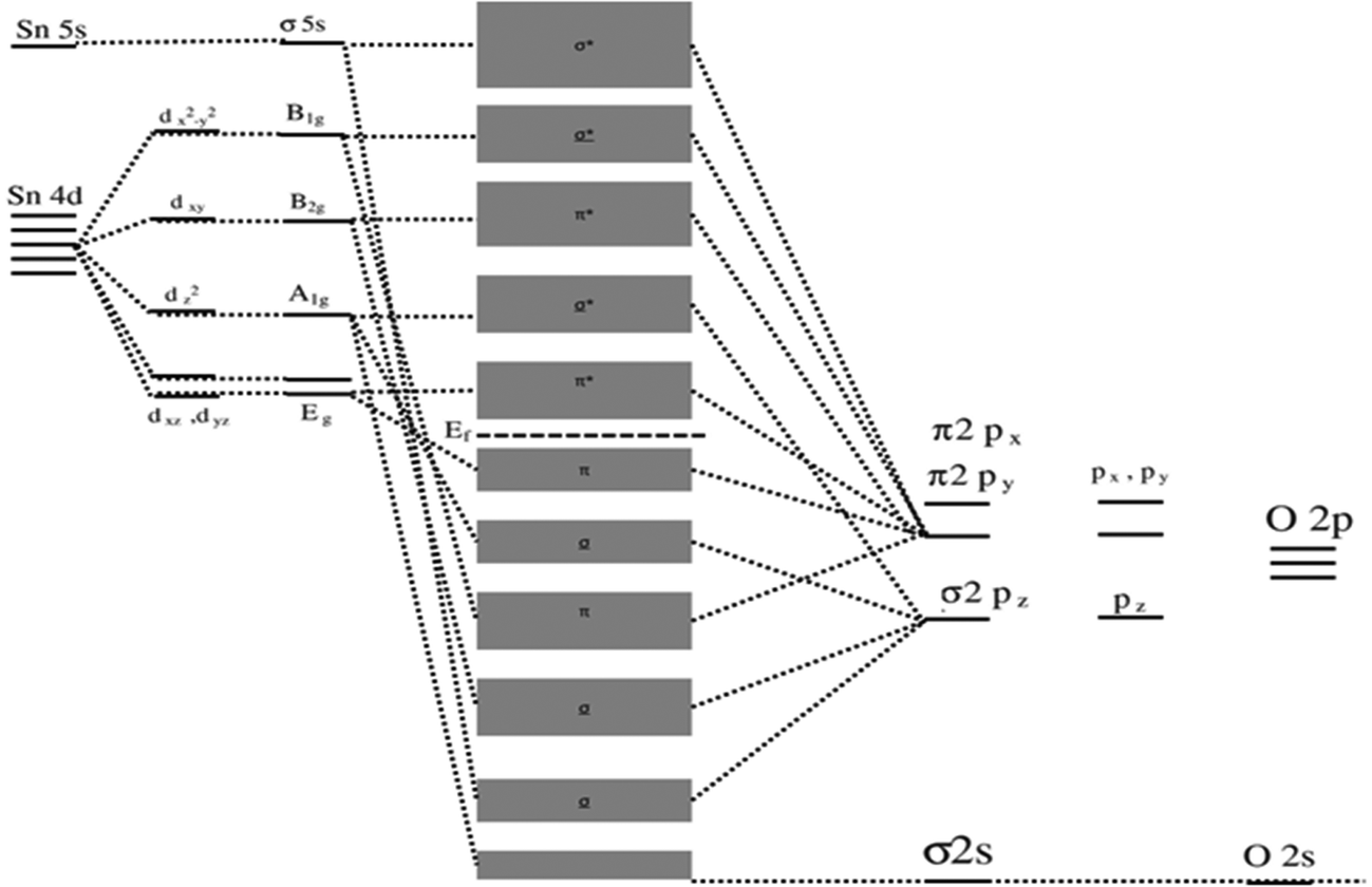 | ||
| Fig. 8 Molecular-orbital bonding structure for tetragonal SnO2. | ||
Hybridization of the B2g, A1g, and Eg orbitals with π2py and σ2pz orbitals among the Sn and O atoms in SnO2 contributes to its electronic structure. Density of states (DOS) can also graphically depict the energy states that electrons occupy in the valence and CBs of SnO2. The CB is primarily influenced by the hybridization of Sn-4d and O-2p orbitals, while the valence band (VB) encompasses contributions from various orbitals, including O-2s, Sn-5s, O-2p, Sn-5p, Sn-4f, Sn-3d, and additional O-2p orbitals.174,175 The presence of defects, such as vacancies in the oxygen or Sn positions within the SnO2 structure, significantly impacts the bonding characteristics and induces distortions in the unit cell.
As a result, these defects change SnO2's bandgap, leading to a reduced value of around 3.5 eV.176 Understanding and controlling the influence of defects is crucial for optimizing SnO2's electronic properties for specific device applications. SnO2 exhibits both direct and indirect bandgap transitions.177,178 Indirect bandgaps are observed at energy levels of 2.62 and 2.90 eV, which include variations in the electronic states within the material.179 Moreover, the fundamental bandgap energy of SnO2 has been predicted to be lower at around 3 eV.180 However, specific optical transitions, known as dipole-forbidden band-to-band transitions, result in an optical bandgap of 3.8 eV.181 These diverse bandgap characteristics offer diverse optical and electronic properties that can be harnessed for various applications.
An analysis of the electronic structure of pure SnO2 was performed by Slassi et al. through DOS and projected DOS, as depicted in Fig. 9; where the impact of the exchange–correlation terms on the distribution of eigenstates was assessed utilizing the (a) GGA-PBE and (b) TB-mBJ approximations. Notably, strikingly similar distributions of the eigenstates were exhibited by the results from both approximations. It was revealed by the DOS that the upper section of the VB extended from −7.8 to 0 eV in the PBE calculation and from −7 to 0 eV in the TB-mBJ calculation, while demonstrating a pronounced O-2p character, with minor contributions from an admixture of 4p and d-Sn states. Furthermore, the lower segment of the CB was predominantly characterized by the 4s-Sn orbital at the G-point.182
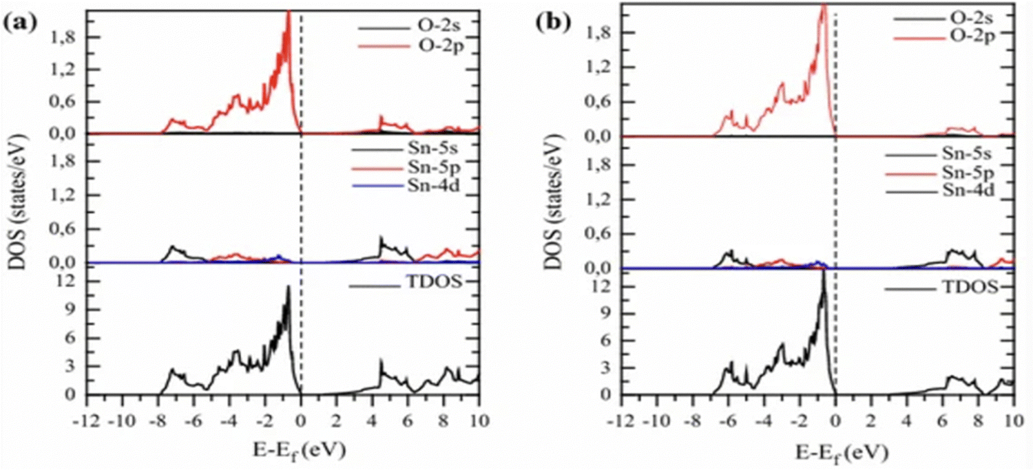 | ||
| Fig. 9 Pure SnO2's partial and total densities of states calculated using (a) GGA-PBE and (b) Tb-mBJ. Reproduced with permission.182 Copyright 2017, Wiley. | ||
2.5. Recent progress of SnO2 as an ETL
Previously, attempts have been made to utilize SnO2 in third-generation solar cells. However, these devices still fall short when compared to using ZnO and TiO2. In 2015, several groups individualistically incorporated SnO2 in PSCs. For example, Dai and colleagues employed mesoporous SnO2 films as an ETL and achieved an efficiency of 10.18% by combining them with TiCl4 treatment.183 Kuang and colleagues employed a nano colloidal film of SnO2 treated with TiCl4 as the ETL. A PSC achieved an efficiency of 14.69% due to this development. Addressing the challenges posed by high-temperature processing, a SnO2 layer was developed that could be processed at lower temperatures.17 The process utilized by Tian's team included applying spin-coated SnO2 nanoparticles on substrates, and then carrying out a subsequent annealing step at 200 °C. As a result of this approach, a PCE of 13% was achieved.184 Notably, Fang and colleagues reported a significant advancement in SnO2-based PSCs by employing decomposition of a SnCl2·2H2O precursor through thermal treatment at 180 °C under normal atmospheric conditions, resulting in a reverse scan efficiency of 17.21% on an FTO substrate.185 Moreover, a low-temperature ALD method was utilized by Hagfeldt and colleagues for the production of SnO2 ETL, resulting in a PCE of approximately 18%, with a Voc exceeding 1.19 V. Despite these results, the performance of these devices continues to lag behind their TiO2 counterparts.186 You et al. achieved a remarkable PCE of 21.6% in photovoltaic cells based on SnO2. This accomplishment was made possible by their control of the surface passivation layer on PbI2. Additionally, they achieved an impressive efficiency rate of 20.9%.187 Zhu et al. introduced a novel approach using a SnO2–KCl composite ETL in planar PSCs. This strategy could simultaneously address defects at the ETL/perovskite interface and grain boundaries. By incorporating K and Cl ions, the ETL/perovskite contact could be effectively passivated, leading to an enhanced Voc from 1.077 V to 1.137 V and increased PCE from 20.2% to 22.2%.188 Zhang's team, focused on reducing electron-transport losses within the ETL of metal oxide-based solar cells, introduced a novel ETL composed of amorphous F-doped TiOx (F-TiOx) and crystalline SnO2. Here, the F-TiOx was an intermediary between adjacent SnO2 nanocrystalline molecules, with enhanced electron-transport pathways, reduced charge losses, and enhanced energy-level alignment. This modification led to a remarkable PCE of 22.70% in PSCs together with improved stability.189 Li's team developed a water-soluble polyelectrolyte combining ethanolamine (EA) and poly-acrylic acid (PAA). They used this to stabilize SnO2 nanoparticles, creating a 3D network. This hybrid material was then integrated into the SnO2 ETL, and helped prevent nanoparticle clumping and enabled a uniform film formation. The PAA–EA-modified SnO2 also improved the perovskite film quality, enhancing carrier transport. As a result, PSCs achieved outstanding PCEs of 24.34% and 22.88% in different areas.190 These advancements are illustrated in Fig. 10, showcasing the progress in PSCs utilizing SnO2 as an ETL in the discussed studies.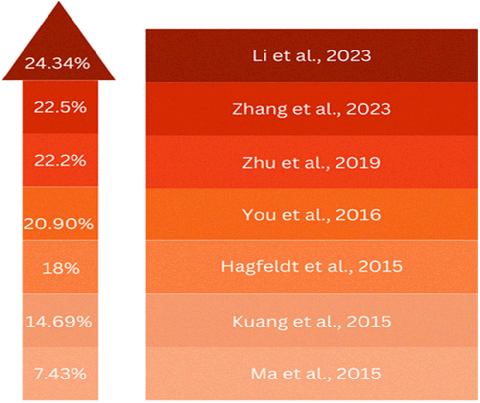 | ||
| Fig. 10 Advancement in SnO2 as an ETL layer in recent years. | ||
A novel method for preparing a mesoporous SnO2 ETL was presented by Sami Ullah and colleagues, involving the anodization of a metallic Sn film on an FTO substrate in a sodium hydroxide solution. A bilayer architecture was employed consisting of two consecutive layers of mesoporous SnO2, with the morphology of each layer controlled by adjusting the anodization voltage and time. This approach allowed for better coverage of the FTO substrate compared to a single-layer configuration. The photovoltaic device incorporating the bilayer mesoporous SnO2 ETL exhibited a notable 27% improvement in PCE. A comparison of the second layer evaporation, as shown in the FESEM image, and improvement in the PCE are shown in Fig. 11 below.191
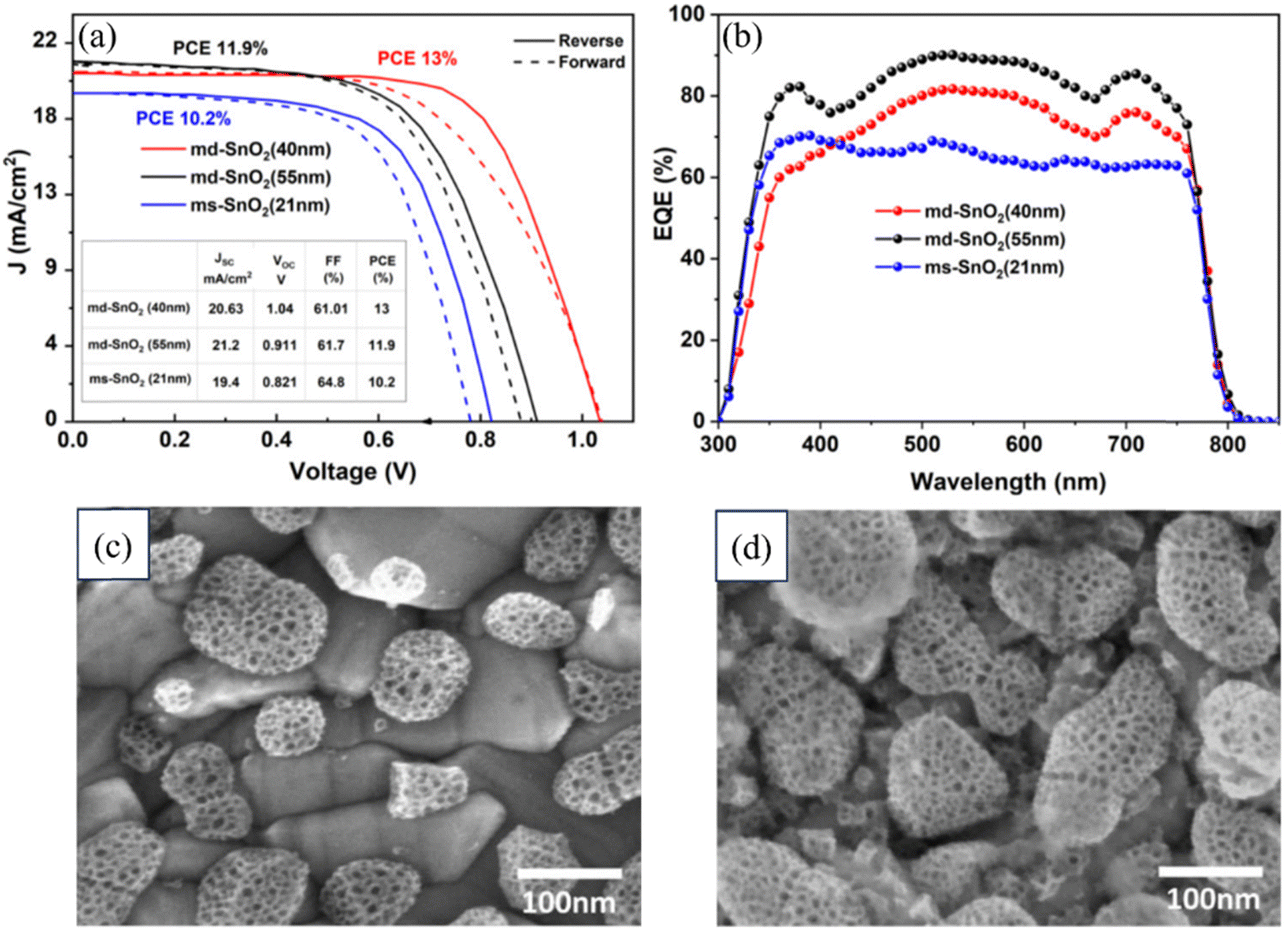 | ||
| Fig. 11 (a) Typical J–V curves of PSCs with md-SnO2 (40 and 55 nm) and ms-SnO2 (21 nm) ETLs. (b) External quantum efficiency spectra of PSCs with md-SnO2 (40 and 55 nm) and ms-SnO2 (21 nm) ETLs. (c) FESEM image of the ms-SnO2 layer grown on the FTO substrate showing the anodized evaporated Sn film. (d) FESEM image of the second Sn layer evaporated on anodized ms-SnO2 in md-SnO2. Reproduced with permission.191 Copyright 2022, American Chemical Society. | ||
Zhengjie Xu, Yue Jiang, and their research team studied the rapid synthesis of SnO2 QDs using a microwave-assisted method for PSCs. The small-sized SnO2-QDs exhibited remarkable electronic properties compared to crystallized SnO2 films, including improvements in the Fermi level, conductivity, electron mobility, and trap density. Additionally, the performance of PSCs based on the CH3NH3PbI3 perovskite material was significantly enhanced, achieving a PCE of 20.24% with a higher Voc compared to the PCE of 19.77% without SnO2-QDs. Fig. 12 illustrates a cross-sectional FESEM image of the tested device and an image showing the SnO2-QD deposition on an FTO substrate. Scale bars of 200 nm are included for reference. Additionally, as previously mentioned, TEM images and details on the device's performance are provided. These findings highlight the great potential of the microwave-assisted synthesis of SnO2-QDs for the efficient, reproducible, and large-scale production of SnO2-QDs.192
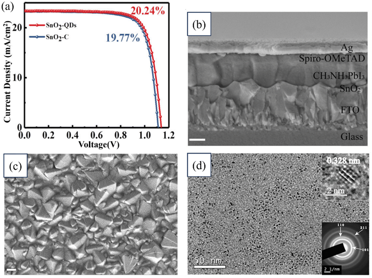 | ||
| Fig. 12 (a) J–V characteristic curves from forward and reverse scans. (b) FESEM image of the cross-section of a tested device. (c) SEM image of SnO2 coated on an FTO substrate. (d) TEM image of SnO2. Reproduced with permission.192 Copyright 2022, American Chemical Society. | ||
Muhammad Salman Kiani researched the synthesis of SnO2 QDs to be used as an ETL in flexible PSCs. QDs of 2.4 nm diameter were produced through a solvothermal synthesis, and exhibited excellent crystallinity and dispersion. Functional layers were applied using a slot-die coating method, and water-based inks with varying QD concentrations were tested. The optimal performance was achieved with 2 wt% SnO2 QD ink, resulting in an average PCE of 7.23% and a peak PCE of around 10%.193 The provided information illustrates a comprehensive analysis of an as-fabricated SnO2 QD-based device, as depicted in Fig. 13. The figure includes the J–V curves, a cross-sectional view of the SnO2 layer captured through FESEM, a micrograph showing the TEM images of the SnO2 QD, and a schematic detailing the fabrication process of the device.
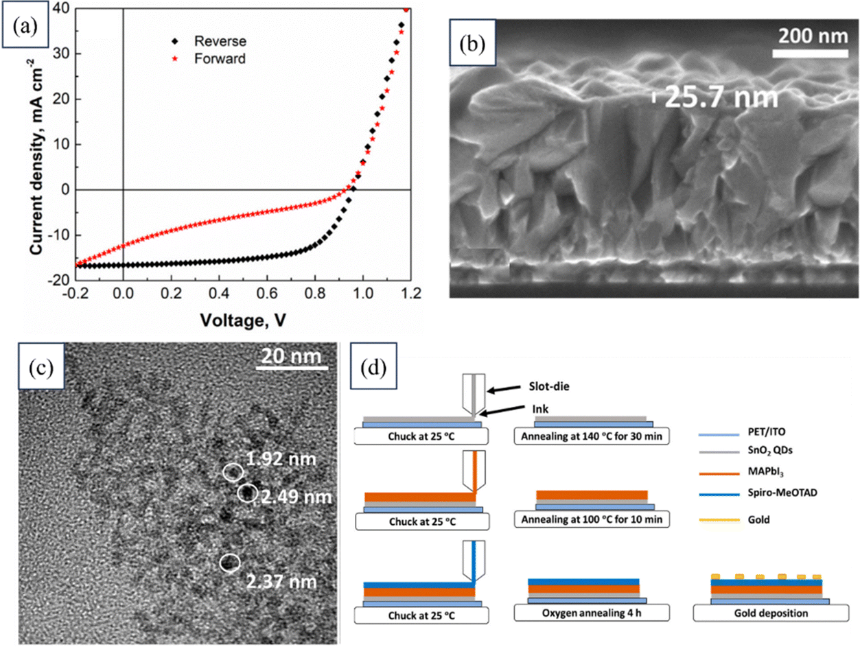 | ||
| Fig. 13 (a) J–V curves of a device based on SnO2 QDs. (b) FESEM image showing the cross-section of the SnO2 layer. (c) TEM image of the SnO2 QD. (d) Schematic of the device fabrication process. Reproduced with permission.193 Copyright 2022, MDPI. | ||
In another study, a novel approach was developed to enhance the electronic-transfer properties of SnO2 layers in PSCs. A small amount of TiAcAc (titanium acetylacetonate) molecules was introduced into a SnO2 nanoparticle solution. The incorporation of TiAcAc served multiple functions: stabilizing the dispersion of SnO2 nanoparticles, enabling the formation of smooth ETL thin films, tuning the electronic band structure to match the upper perovskite layer, and improving the interface properties between the ETL and the perovskite layer. By varying the doping concentration, the thin-film morphology, surface energy, and optoelectronic properties of the SnO2 ETL could be finely adjusted. This innovative approach could significantly improve the efficiency and reduce hysteresis in PSCs, comparable to state-of-the-art SnO2-based PSCs. The findings of this research offer a promising and efficient method for controlling SnO2 growth, which could ultimately lead to highly efficient PSCs. Fig. 14 illustrates the typical J–V curves for a device utilizing SnO2–TiAcAc. It highlights the expected influence of depositing perovskite on thin films composed of TiAcAc-doped SnO2 nanoparticles. Additionally, FESEM images are provided showing the SnO2 layer deposited on FTO and the SnO2–TiAcAc layer deposited on FTO.194
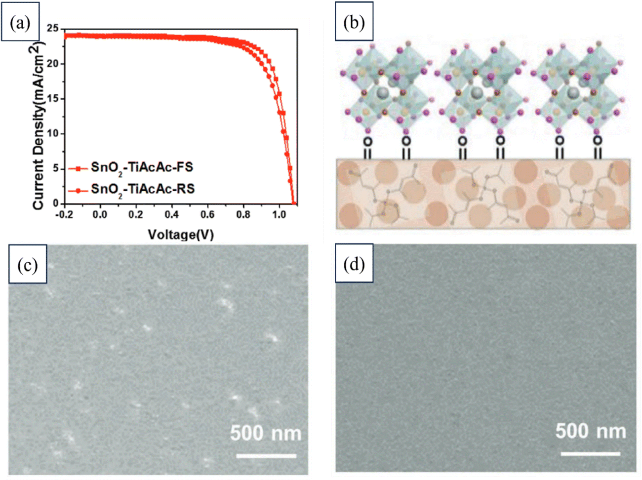 | ||
| Fig. 14 (a) Typical J–V curves of a device based on SnO2–TiAcAc. (b) Anticipated impact of depositing perovskite on thin films of TiAcAc-doped SnO2 nanoparticles. FESEM images of (c) SnO2 layer deposited on FTO and (d) SnO2–TiAcAc deposited on FTO. Reproduced with permission.194 Copyright 2021, Wiley. | ||
Gu and Bangkai's team enhanced the performance of SnO2 ETL-based PSCs using bipyramidal quantum dots (BPQDs). The SnO2/BPQDs mixture achieved a remarkable 21% efficiency, with sustained stability (over 90% efficiency after 1000 h of AM 1.5G lamp exposure) and minimal hysteresis. Fig. 15 displays the performance, specifically the J–V curves, employing different ETL configurations, namely in single SnO2, BPQDs/SnO2 bilayer, SnO2/BPQDs mixed, and SnO2/BPQDs bilayer ETL-based PSCs. Additionally, the figure includes FESEM images illustrating the morphology of a single SnO2, SnO2/BPQDs mixed sample, and a TEM image providing a closer look.154
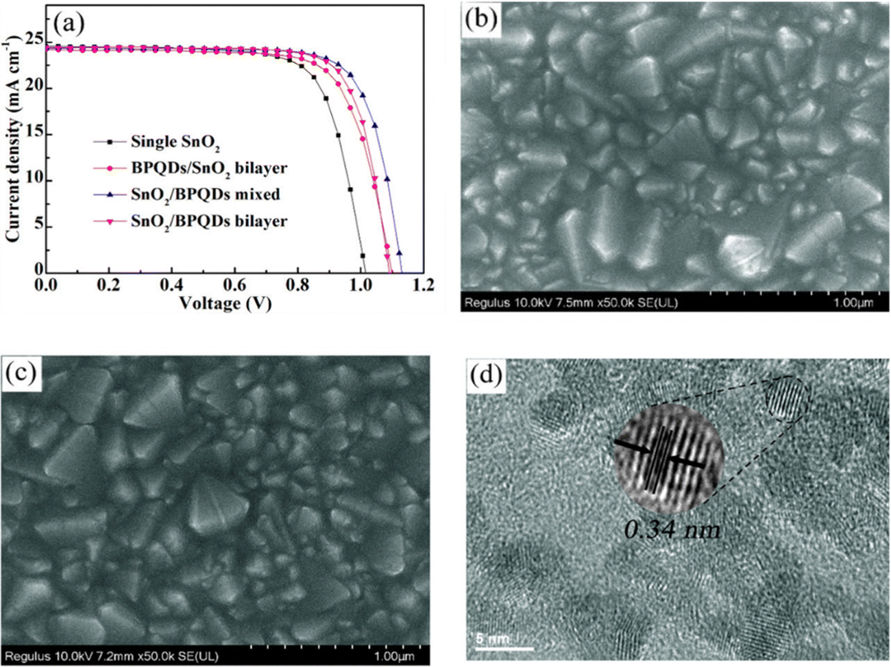 | ||
| Fig. 15 (a) J–V curves of single SnO2, BPQDs/SnO2 bilayer, SnO2/BPQDs mixed, and SnO2/BPQDs bilayer ETL-based PSCs, FESEM images of (b) single SnO2, (c) SnO2/BPQDs mixed sample. (d) TEM image. Reproduced with permission.154 Copyright 2022, American Chemical Society. | ||
Babak Taheri's team demonstrated a scalable manufacturing process for large-area PSCs that is compatible with various surfaces for industrial applications. They introduced the concept of automated spray-coating (ASC) (at low temperatures) and utilized Np-SnO2 as an effective strategy for creating expansive PSCs and modules. Fig. 16 presents the PCEs of all the solar devices fabricated using SnO2, which were spray-coated at various temperatures, alongside that of a spin-coated device. The figure also includes a schematic depiction of the SnO2 deposition process, highlighting the spray setting parameters. Additionally, top-view SEM images of both spin-coated and spray-coated samples are provided, along with the surface roughness analysis results for both coating methods. This work enables fabricating stabilized planar PSCs through a low-cost, industrial printing technique.195
 | ||
| Fig. 16 (a) PCEs of complete solar devices based on SnO2 spray-coating at different temperatures along with that of a spin-coated device. (b) Schematic representation of SnO2 deposition with the spray setting parameters, (c) top-view SEM images of spin-coated and spray-coated samples, and (d) surface roughness analysis of spin-coated and spray-coated samples. Reproduced with permission.195 Copyright 2020, Wiley. | ||
Zhuldyz Yelzhanova's team investigated the impact of various growth parameters on solvothermal-grown SnO2 nanostructures. They studied factors like the growth pressure, substrate orientation, solvent ratios, seed layer types, and growth time. Key findings included that adjusting the precursor volume could optimize the pressure, the substrate orientation affects the nanorod growth direction, and the solvent ratios influence the nanorod density. They noted that the seed layers on FTO significantly influenced the SnO2 structure morphology. Elongated nanorods were used using a two-step solvothermal method, but the thickness increase remained challenging. For PSCs, employing solvothermal SnO2 nanostructures as ETLs required oxygen plasma surface treatment to enhance the photovoltaic performance. Fig. 17 presents the current–voltage characteristics of photovoltaic cells utilizing SnO2 nanorod arrays, with and without oxygen plasma treatment. Moreover, SEM top-view and cross-sectional images are displayed for the SnO2 nanostructures grown in autoclaves of differing volume sizes: (a, d) 25 mL, (b, e) 50 mL, and (c, f) 100 mL. Additionally, SEM images of the samples exposed to solvothermal growth depict various mounting orientations: (a, d) 45°, (b, e) 90°, and (c, f) 0°. Insights for optimizing the SnO2 nanostructure growth and for application in photovoltaic devices are provided in this study.196
 | ||
| Fig. 17 (A) Current–voltage behaviours in photovoltaic cells employing SnO2 nanorod arrays with and without oxygen plasma treatment. (B) SEM top-view and cross-sectional images showcasing SnO2 nanostructures grown in different autoclave volumes: (a) and (d) 25 mL, (b) and (e) 50 mL, and (c) and (f) 100 mL. Additionally, (C) SEM top and cross-sectional images for samples mounted in various orientations for solvothermal growth: (a) and (d) 45°, (b) and (e) 90°, and (c) and (f) 0°. Reproduced with permission.196 Copyright 2022, MDPI. | ||
Xiangqing Zhou's team innovatively developed a low-temperature method using Cu-doped SnO2 as an ETL in planar PSCs. This yielded a remarkable PCE of 21.35%, surpassing the 19.63% of the control device. Cu doping improved SnO2 conductivity and energy-level alignment, enhancing electron extraction, charge transfer, and reducing charge recombination at the SnO2/perovskite interface. The Cu:SnO2 ETL also enhanced the perovskite film quality, leading to more prominent grains and better light absorption and improved Jsc and FF values. The PSC device with the Cu:SnO2 ETL also demonstrated exceptional stability under light and thermal conditions, outperforming the reference device. Fig. 18 presents the J–V characteristics of photovoltaic devices employing SnO2 and a 5% copper-doped tin dioxide Cu:SnO2 as the ETL. Additionally, the figure includes FESEM images depicting the cross-section of a device with SnO2 as the ETL, another featuring a Cu-doped SnO2 ETL, and a third showcasing the cross-section of a device utilizing Cu-doped SnO2 as the ETL.197
 | ||
| Fig. 18 (a) J–V characteristics of photovoltaic devices utilizing SnO2 and a 5% copper-doped tin dioxide (Cu:SnO2) ETL. FESEM images of (b) cross-section of the device with SnO2 as the ETL, (c) Cu-doped SnO2, (d) cross-section of the device with Cu-doped SnO2 as the ETL. Reproduced with permission.197 Copyright 2022, Elsevier. | ||
A novel interface modification for planar PSCs was introduced by Razieh Keshtmand's team utilizing SnO2 and NH4Cl. The electronic properties of SnO2 were enhanced by NH4Cl, while the defects at the ETL/perovskite interface were mitigated. A significant 20% efficiency increase was achieved by the modified SnO2 (SnO2–Cl3) ETL variant, attributed to the improved charge transport, reduced recombination, and smoother morphology. Both SnO2 and modified SnO2 were utilized as ETLs in the device, as illustrated by the J–V curves in Fig. 19. Also shown in that figure are FESEM images of the SnO2–Cl3 sample coated on FTO, a cross-section of the device employing SnO2–Cl3, and the perovskite layer deposited on SnO2–Cl3, which served as the ETL. Notable stability was also observed, with the strategy retaining 78% of its initial PCE over 30 days. This strategy offers the potential to enhance the efficiency and stability of PSCs.198
 | ||
| Fig. 19 (a) J–V curves of devices based on SnO2 and modified SnO2 as the ETL. FESEM images of (b) SnO2–Cl3 sample coated on FTO, (c) cross-section of a device based on SnO2–Cl3, (d) perovskite deposited on the SnO2–Cl3 ETL. Reproduced with permission.198 Copyright 2022, Elsevier. | ||
Huiming Luo's team implemented an ethanol treatment method to enhance the conductivity of SnO2 film in order to improve the efficiency of PSCs and reduce hysteresis. Fig. 20 illustrates the J–V curves for devices utilizing SnO2 and EtOH–SnO2 as ETLs. Additionally, the cross-sectional FESEM image of the device along with FESEM images depicting the deposited SnO2 layer and EtOH–SnO2 are presented. Consequently, the PSCs utilizing ethanol-treated SnO2 as the ETL exhibited a noteworthy PCE rising from 20.70% to 21.62%, accompanied by a substantial increase in Jsc. Additionally, the PSCs encapsulated with EtOH–SnO2 showed only a 20% degradation in efficiency after 1000 h of light soaking. Even the unencapsulated devices retained 80% of their original efficiency after continuous heating on an 85 °C plate for 300 h. These findings indicate that ethanol treatment could positively affect the conductivity of the SnO2 layer and the overall performance of PSCs.199
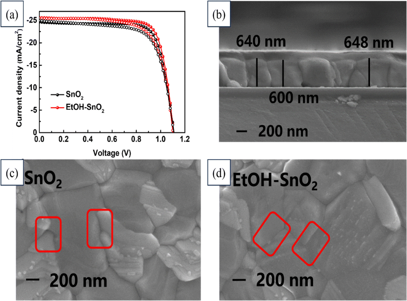 | ||
| Fig. 20 (a) J–V curves of devices based on SnO2 and EtOH–SnO2 as ETLs. FESEM images of (b) cross-section of the device, (c) deposited SnO2 layer, and (d) EtOH–SnO2. Reproduced with permission.199 Copyright 2022, Elsevier. | ||
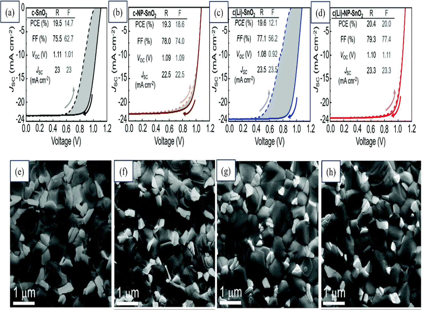
An extensive investigation was conducted on various single- and bilayer SnO2 ETLs by Abed Alrhman Eliwi's team with an aim to enhance the efficiency of planar n–i–p PSCs. Through XPS analysis, they confirmed the successful doping of Li in the c(Li)-SnO2 ETL and the presence of K in ETLs formed using a commercial SnO2 NP colloidal solution. A ground-breaking bilayer c(Li)-NP-SnO2 ETL was introduced that ingeniously combined the advantages of Li and K. Improved charge extraction was achieved, effectively suppressing ion migration and reducing charge accumulation at the perovskite/ETL interface. The exceptional performance of the developed double-cation PSC with c(Li)-NP-SnO2 ETL was demonstrated, whereby a remarkable PCE of 20.4% was exhibited in the −V scan and, even more impressively, a stabilized PCE of around 18.5% was maintained after MPP tracking for 300 s. Notably, substantially reduced hysteresis and significant enhancements in both the FF and Jsc were demonstrated by this champion PSC compared to other optimized ETL configurations, as shown in Fig. 21. This figure also shows FESEM images of the perovskite-coated layers of these SnO2 layers.200
 | ||
| Fig. 21 Reverse (R) and forward (F) J–V scans and stabilized PCE (s-PCE) derived from MPP tracking of champion PSCs with (a) c-SnO2, (b) c-NP-SnO2, (c) c(Li)-SnO2, and (d) c(Li)-NP-SnO2 ETLs. Top SEM images of perovskite thin films deposited on (e) c-SnO2, (f) c-NP-SnO2, (g) c(Li)-SnO2, and (h) c(Li)-NP-SnO2 ETLs. Reproduced with permission.200 Copyright 2022, Royal Society of Chemistry. | ||
Haibing Wang's team proposed a simple yet effective strategy by incorporating H2O2 into the commonly used SnO2 colloid precursor, and revealed this could enhance the ETL quality, while reducing trap densities and making electron extraction more efficient. Introducing H2O2 into the SnO2 precursor also aligned the Fermi level of the H2O2–SnO2 ETL better with the perovskite's CB, thereby benefiting an improvement in the Voc. Moreover, perovskite grown on the H2O2–SnO2 substrate demonstrated fewer trap densities. Employing H2O2–SnO2 as the ETL yielded significant enhancements in PSC performance, long-term stability, and device fabrication repeatability. Fig. 22 illustrates the J–V characteristics of devices utilizing SnO2 and H2O2–SnO2 ETLs. The schematic diagram depicts the employed process, while the top-view SEM images showcase the pristine SnO2 film, and H2O2–SnO2 film. This pioneering study revealed the impact of H2O2 on enhancing the SnO2 ETL, offering a novel approach for boosting PSC efficiency and device fabrication consistency. Further, this strategy introduces a new direction for designing SnO2-based devices based on the reduction of oxygen defects.201
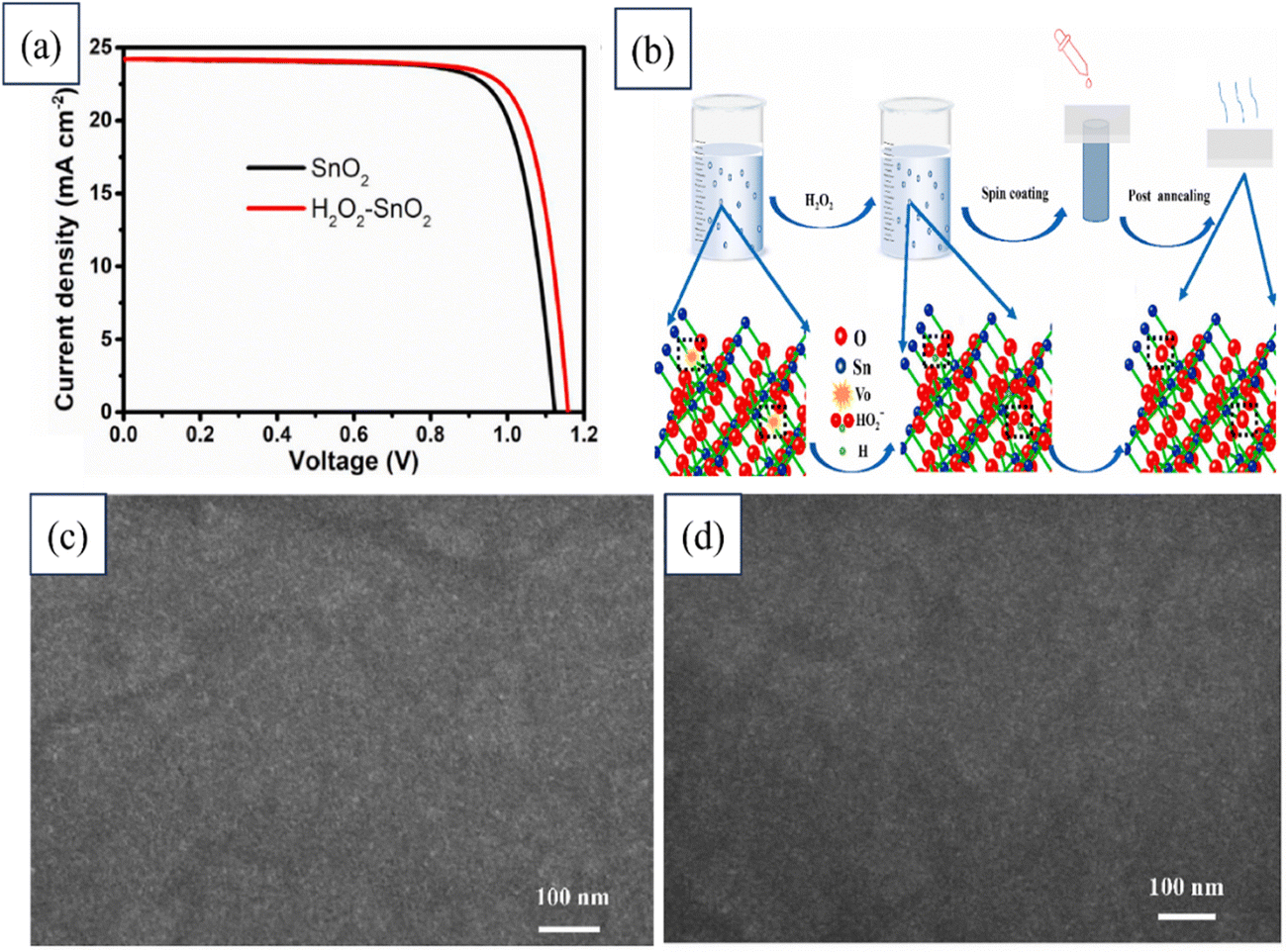 | ||
| Fig. 22 (a) J–V characteristics of devices with SnO2 and H2O2–SnO2 ETLs. (b) Schematic illustration of process used. Top-view SEM images of (c) pristine SnO2 film, and (d) H2O2–SnO2 film. Reproduced with permission.201 Copyright 2021, Elsevier. | ||
Enqi Wang and colleagues effectively showcased a novel approach to enhance the efficacy of SnO2 ETLs through ethanol vapour treatment during annealing. In contrast to conventional annealing techniques, this method substantially enhanced the electrical characteristics of the SnO2 film. Additionally, when the perovskite light-absorbing layer was applied to the ethanol-treated SnO2 film, it yielded heightened light absorption and a diminished density of trap states in the light-absorbing material. Consequently, PSCs produced using the ethanol-treated SnO2 film as the ETL demonstrated enhanced electron injection and transfer, leading to minimized charge recombination. These advancements resulted in improved Voc and FF values, culminating in an impressive 17.66% PCE. Fig. 23 presents the J–V curves of the device, illustrating the impact of ethanol vapour treatment on the SnO2 film. The schematic of the experimental set-up for ethanol vapour is presented, along with SEM images showcasing the SnO2 layer deposited in ethanol vapour and a cross-section of the tested device. These remarkable findings introduce a fresh avenue for enhancing the PCE in PSCs by subjecting the ETL to ethanol vapour treatment during the annealing process.202
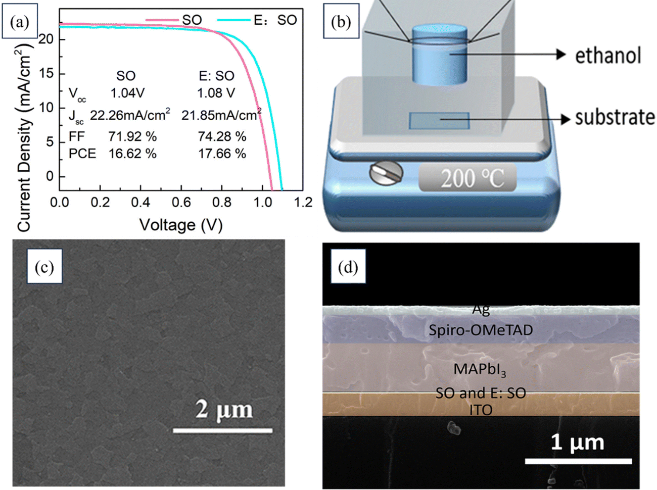 | ||
| Fig. 23 (a) J–V curves of a device based on the SnO2 film with and without ethanol vapour treatment. (b) Schematics of the ethanol vapour experimental set-up. SEM images of (c) SnO2 layer deposited in ethanol vapour and (d) cross-section of the tested device. Reproduced with permission.202 Copyright 2020, Elsevier. | ||
Table 11 gives an overview of the synthesis methods, device structures, and their respective solar cell parameters, from which it can be seen that spin-coating emerges as a highly effective deposition method in the realm of PSC fabrication, consistently demonstrating favourable outcomes with notable PCE values ranging from 10.18% to 20.9%. Remarkably, certain devices even surpassed the 20% threshold, underscoring the significant potential of this technique for enhancing PSC technology. In particular, devices incorporating FTO/SnO2 as the ETL exhibited a desirable PCE and FF, indicating the efficacy of this specific ETL combination in improving device performance. Additionally, the highest PCE of 20.9% achieved through spin-coating underscores its promising applicability in producing PSCs with enhanced efficiency. Despite the prominence of spin-coating, alternative deposition methods, such as ALD, also show promise, yielding devices with respectable PCE values. Conversely, hydrothermal and electrodeposited approaches exhibit relatively lower PCE values, suggesting the necessity for further optimization efforts in these deposition methods to enhance their performance in PSC applications. Overall, while spin-coating with FTO/SnO2 as the ETL presents a consistent and promising option, the exploration of other methods, like ALD and solution-processed chemical bath deposition (SC-CBD), holds potential for achieving high PCE values in PSCs.
| Deposition method | Device structure | V oc [V] | J sc [mA cm−2] | FF [%] | PCE [%] | Ref. |
|---|---|---|---|---|---|---|
| SC-CBD | FTO/SnO2/(FAPbI3)(MAPbBr3)/spiro-/Au | 1.18 | 22.73 | 77 | 20.78 | 203 |
| Electrodeposition | ITO/SnO2/MAPbI3/spiro-/Ag | 1.08 | 19.75 | 65 | 13.88 | 204 |
| Spin-coating | ITO/SnO2/(FAPbI3)(MAPbBr3)/spiro-/Au | 1.09 | 24.88 | 75.73 | 19.9 | 205 |
| PLD | FTO/SnO2/PCBM/MAPbI3/spiro-/Au | 1.11 | 21.6 | 71 | 17.03 | 203 |
| Spin-coating | ITO/SnO2/MAPbI3/spiro-/Au | 1.15 | 21.74 | 80.9 | 20.23 | 206 |
| Spin-coating | FTO/SnO2/MAPbI3/spiro-/Au | 1.023 | 21.19 | 67.8 | 14.69 | 207 |
| Spin-coating | FTO/SnO2/(FAPbI3)(MAPbBr3)/spiro-/Au | 1.13 | 23.05 | 79.8 | 20.79 | 208 |
| Spin-coating | FTO/Nb:SnO2/MAPbI3/spiro-/Au | 1.08 | 22.36 | 72.7 | 17.57 | 209 |
| ALD | FTO/SnO2/(FAPbI3)(MAPbBr3)/spiro-/Au | 1.14 | 21.3 | 74 | 18.4 | 210 |
| Spin-coating | ITO/SnO2/(FAPbI3)(MAPbBr3)/spiro-/Au | 1.12 | 23.86 | 80.6 | 20.9 | 211 |
| Spin-coating | FTO/SnO2nanosheet/MAPbI3/spiro-/Au | 1.11 | 23.27 | 67 | 17.21 | 212 |
| Spin-coating | FTO/bl-SnO2/mp-SnO2/MAPbI3/spiro-/Au | 0.933 | 17.38 | 62.8 | 10.18 | 213 |
| PEALD | FTO/SnO2/C60 -SAM/MAPbI3/spiro-/Au | 1.13 | 21.56 | 78.11 | 19.03 | 214 |
| Hydrothermal | FTO/SnO2nanosheet/MAPbI3/spiro-/Au | 1.05 | 22.76 | 68 | 16.17 | 215 |
| Spin-coating | ITO/SnO2/(FAPbI3) (MAPbBr3)/EH44/MoOx/Al | 1.091 | 21.71 | 77.9 | 18.5 | 216 |
2.6. Modification strategies of SnO2 as ETLs
Modifications of the photoanode are often utilized to mitigate electron recombination phenomena in photovoltaic devices. Various strategies, such as elemental doping, incorporating additional ETLs, and surface modifications, have been extensively utilized for modifying SnO2-based photoanodes. Significant improvements in the performance of photovoltaic devices have been demonstrated through these modifications, particularly in the following aspects: (1) the passivation of surface states can be facilitated by elemental doping, leading to a reduction in recombination rates; (2) the morphology of the absorber layer can be enhanced and intimate contact at the interface promoted by modifications, also enhancing charge-transfer efficiency; (3) the long-term stability and durability of photovoltaic systems can be significantly enhanced by modification of the photoanodes.| Doped elements | V oc [V] | J sc [mA cm−2] | FF [%] | PCE (%) | Ref. |
|---|---|---|---|---|---|
| Ta5+ | 1.161 | 22.79 | 78.6 | 20.80 | 217 |
| Ta5+ | 1.08 | 22.73 | 73.5 | 18.23 | 218 |
| Cl− | 1.195 | 22.1 | 75.6 | 20 | 219 |
| Cl− | 1.1 | 23.02 | 69 | 18.1 | 220 |
| Li+ | 1.065 | 21.65 | 67.42 | 15.54 | 221 |
| Li+ | 0.909 | 19.97 | 76 | 18.35 | 222 |
| Li+ | 1.106 | 23.27 | 70.71 | 18.2 | 223 |
| MSE-Na+ | 1.12 | 23.88 | 78.69 | 21.05 | 224 |
| 1%-Sc | 1.108 | 23.12 | 75.03 | 19.19 | 225 |
| 2%-Sc | 1.113 | 23.24 | 75.64 | 19.56 | |
| 3%-Sc | 1.117 | 23.36 | 76.80 | 20.03 | |
| 4%-Sc | 1.016 | 20.87 | 69.05 | 14.64 | |
| 1%-Y | 1.109 | 23.21 | 74.94 | 19.30 | |
| 2%-Y | 1.112 | 23.35 | 76.56 | 19.81 | |
| 3%-Y | 1.117 | 23.61 | 78.16 | 20.63 | |
| 4%-Y | 1.029 | 21.02 | 70.03 | 15.15 | |
| 1%-La | 1.106 | 23.11 | 74.79 | 19.13 | |
| 2%-La | 1.107 | 23.16 | 75.15 | 19.28 | |
| 3%-La | 1.111 | 23.21 | 75.57 | 19.49 | |
| 4%-La | 1.011 | 20.88 | 67.22 | 14.19 | |
| La | 1.08 | 21.61 | 78.17 | 18.36 | 226 |
| Mg2+ | 1.1 | 21.68 | 70.5 | 16.82 | 221 |
| Sb5+ | 1.094 | 22.3 | 70 | 17.07 | |
| Sb5+ | 1.06 | 22.6 | 72.0 | 17.2 | 230 |
| Al3+ | 0.85 | 19.0 | 62 | 10.8 | 227 |
| Al3+ | 1.09 | 21.82 | 77.61 | 18.45 | 226 |
| 2.5% Zn–SnO2 | 0.99 | 19.51 | 49.65 | 49.65 | 228 |
| 5% Zn–SnO2 | 1.01 | 19.57 | 51.58 | 10.21 | |
| 7.5% Zn–SnO2 | 1 | 19.47 | 50.1 | 9.77 | |
| Zn–SnO2 | 1.098 | 23.4 | 69.2 | 17.78 | 229 |
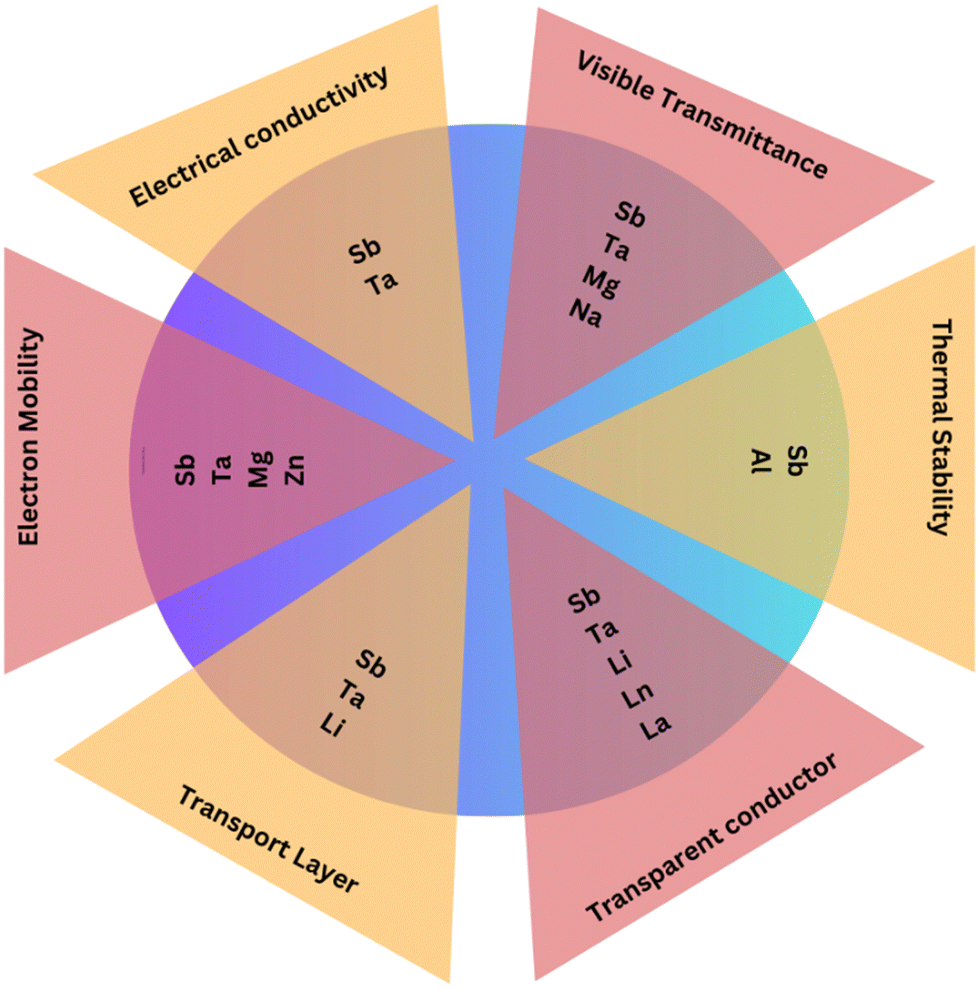 | ||
| Fig. 24 Graphical representation of the effect of doping in SnO2 on different physical properties. | ||
2.6.2.1. SnO2/metal oxide ETLs. In photovoltaic systems utilizing the n–i–p architecture, bilayer metal oxide composite configurations are frequently employed as ETLs. Mali et al. selected SnO2-coated c-TiO2 bilayer ETLs to take advantage of the high electron mobility of SnO2 compared to TiO2. Surface traps in the TiO2 film were suppressed by the SnO2 layer, allowing the effective extraction of electrons from the perovskite layer and the preservation of charge balance in the device.231
Wang et al. developed an In2O3/SnO2 bilayer ETL prepared through a low-temperature process. The introduction of In2O3 resulted in smooth and low-defect-density perovskite films. The lower CB of In2O3 compared to Sn-doped In2O3 (ITO) promoted charge transfer at the interface, reducing voltage loss. The device achieved a high PCE of over 23% and demonstrated good stability.232 A novel amorphous WOx/SnO2 hybrid ETL was proposed by Wang et al. to block holes and enhance charge extraction effectively. The appropriate energy-level alignment and high conductivity of the hybrid ETL facilitated electron transfer. Flexible PSCs with the hybrid ETL exhibited a higher PCE of 20.52% compared to those with the single SnO2 ETL.233 Ye et al. developed a doped SnO2 bilayer ETL composed of two different SnO2 films combined with NH4Cl as an additive. This bilayer structure could tune the bandgap alignment at the SnO2/perovskite interface, reducing strain in the perovskite film growth and minimizing carrier recombination. The optimized device with the doped SnO2 bilayer ETL achieved a remarkable PCE of 21.75% and increased the Voc to 1.21 V, with negligible hysteresis.234 The effectiveness of bilayer ETLs incorporating SnO2 in improving the performance and stability of PSCs by suppressing defects, enhancing charge extraction, and optimizing bandgap alignment at the interface was demonstrated by these studies.
2.6.2.2. SnO2/fullerene derivative ETLs. Caruso and colleagues showed that incorporating C60 onto the surface of SnO2 nanosheets led to the partial occupancy of the surface trap states, neutralising both interfaces: C60/perovskite and SnO2/C60. The enhanced alignment of the bands decreased the recombination of charges between electrons and holes that were injected by light into the perovskite layer. This led to an improved Voc and effectively suppressed the recombination of charges.235
Surface modification with a SnO2/C60 self-assembled monolayer (SAM). Like various metal oxides, SnO2 can establish robust electronic coupling with a self-assembled monolayer of C60. This interaction allows for better surface characteristics and the mitigation of ion migration. Jen et al. and Yan et al. reported impressive PCEs of 15% while minimizing hysteresis by introducing a C60-SAM to the SnO2 surface. Nevertheless, the slow process of anchoring SAMs poses obstacles to large-scale manufacturing.236
SnO2/PCBM bilayer. Fang and colleagues achieved a 19.12% PCE using a bilayer approach. This method mitigated the perovskite layer's defects within grains by incorporating dissolved PCBM. At the same time, the interface retained a fragile layer of fullerene, leading to an improved extraction of charges. The development of new fullerenes that are insoluble in perovskite solvent could improve the reproducibility.237
SnO2/graphene quantum dots (GQDs) composite. A SnO2/graphene quantum dots (GQD) composite was employed by Yu et al. and achieved a PCE of 20.23%. The device performance was improved by incorporating the GQDs, which aided in transporting electrons generated by light to the CB of SnO2. Electron-trap sites were effectively occupied in this process, leading to an enhancement of the Fermi level and conductivity within SnO2. Additionally, interfacial recombination between the ETL and perovskite was reduced.238Table 13 provides a comprehensive overview of the effects of SnO2 modifications, encompassing deposition methods, device structures, and associated solar cell parameters, for promoting a thorough understanding in this area.
| Deposition method | Device structure | V oc [V] | J sc [mA cm−2] | FF [%] | PCE (%) | Ref. |
|---|---|---|---|---|---|---|
| Spin-coating | FTO/SnO2/PCBM/MAPbI3/spiro-/Au | 1.12 | 22.61 | 75.8 | 19.12 | 238 |
| Spin-coating | ITO/In2O3/SnO2/perovskite/spiro/Au | 1.17 | 24.45 | 87.09 | 23.24 | 235 |
| PEALD | FTO/SnO2/C60-SAM/MAPbI3/spiro-/Au | 1.13 | 21.56 | 78.11 | 19.3 | 237 |
| Hydrothermal | FTO/SnO2 nanosheet/C60/MAPbI3/spiro-/Au | 1.039 | 23.62 | 75 | 18.31 | 238 |
| Spin-coating | ITO/P-SnO2/B-SnO2/perovskite/spiroOMeAD/Au | 1.21 | 23.6 | 76.2 | 21.75 | 235 |
| Spin-coating | ITO/SnO2:GQDs/MAPbI3/spiro-/Au | 1.134 | 23.05 | 77.8 | 20.31 | 237 |
| Vacuum thermal evaporation | FTO/SnO2/TiO2/perovskite/spiro-OMeTAD/Ag | 1.11 | 23.01 | 80.34 | 20.52 | 233 |
3. Role of Sn in the absorber layer
Solar power as a clean and renewable energy source has gained momentum in recent decades, offering a solution to reduce reliance on fossil fuels. However, the presence of toxic lead in traditional lead halide PSCs raises concerns. To address this issue, researchers are focusing efforts on lead-free alternatives, for ensuring high performance and mitigating environmental and health risks. Materials such as MAPbI3 and FAPbI3, which are lead halide perovskites, have exhibited improved PCEs due to their optoelectronic properties, including direct bandgap, high charge-carrier lifetime, high mobility, and strong light absorption. These attributes underpin their exceptional performance.239–241 Yet, Pb toxicity poses challenges, and is linked to severe health effects and is subject to strict bans by bodies like the EU due to its potential harm to health and the environment.242,243 Stability issues further hamper the use of lead halide PSCs, which are susceptible to degradation from factors like moisture, rain, heat, and air exposure. Outdoor installation compounds these concerns. Researchers are actively aiming to develop lead-free perovskite materials with comparable or better performance.244–246 These materials can offer safer, sustainable options for solar cell technology, addressing the health and environmental risks associated with lead. Their development aligns with the global sustainability agenda, prioritizing safe, eco-friendly, and socially responsible technologies. As clean energy demand rises, ensuring technology safety and sustainability are becoming vital.One approach that has been newly developed to tackle the Pb toxicity problem involves the replacement of every two Pb2+ cations with one monovalent cation and one trivalent cation. This results in the formation of charge-ordered double perovskites with the general formula A2BIBIIIX6. Among the various compositions featuring double perovskite structures, Cs2SnI6 is considered an important material in the photovoltaics community, and is known for its superior stability and optimal bandgap. Also, its intrinsic resistance to oxidation addresses the Pb toxicity concerns. However, Cs2SnI6 remains a rarely explored material, and needs further in-depth study to unlock its optoelectronic potential.
3.1. Synthesis methods
![[thin space (1/6-em)]](https://www.rsc.org/images/entities/char_2009.gif) :1 molar ratio between the two precursor sources, maintaining a constant substrate rotation speed of 10 rpm, and intentionally avoiding substrate heating. The stability of the as-deposited CH3NH3SnI3 thin films was observed for up to months when they were stored in a nitrogen-filled glove box in the dark.248
:1 molar ratio between the two precursor sources, maintaining a constant substrate rotation speed of 10 rpm, and intentionally avoiding substrate heating. The stability of the as-deposited CH3NH3SnI3 thin films was observed for up to months when they were stored in a nitrogen-filled glove box in the dark.248
A solution-based method for MASnI3 perovskite layer fabrication was adopted by Fujihara et al. Here, glass substrates with ITO underwent cleaning through ultrasonication and ultraviolet-ozone treatment. Deposition of the hole-transporter poly(3,4-ethylenedioxythiophene) polystyrene sulfonate (PEDOT:PSS) on the substrates was performed via a two-step spin-coating process, followed by annealing. The precursor solution was then utilized, consisting of MAI, SnI2, and SnF2, in dimethyl sulfoxide (DMSO) in a specific molar ratio. In the SB method for Pb perovskites, MAI and MAPbI3 were slightly dissolved in toluene, with toluene serving as an anti-solvent.249 Ambient room condition synthesis was explored by Swati et al. using an anti-solvent crystallization technique. A stirred equimolar ratio of SnI2 and MAI was employed in diethyl ether or toluene at 50 °C overnight. To obtain the MASnI3 perovskite powder, the precursor solution underwent evaporation using a hot plate and was then annealed at 180 °C. For MASnI3 perovskite films, the precursor solution was combined with toluene and sprayed onto an Au/Ti-coated polyimide substrate using an airbrush via a nitrogen gas flow. The deposition of Ti (10 nm)-buffered Au (100 nm) bottom electrodes onto a polyimide substrate was carried out via direct current (dc) sputtering.250
In the distinct approach of Zhun Yao et al., MASnI3 wafers were prepared by an elaborate process. First, CH3NH3I (MAI) was prepared by reacting HI and MA with a molar ratio of 1:1.2. Freshly synthesized MAI and SnO were dissolved in a mixed solvent of HI and H3PO2 at 80 °C, leading to the formation of a transparent yellow precursor solution. The solution was then gradually cooled to 98 °C over 12 h, allowing tiny crystalline seeds to form on the solution surface. With extending the reaction time, these seeds grew into larger wafers, eventually sinking into the solution as they became enlarged. This meticulous process showcased an alternative route for the synthesis of MASnI3 wafers.251
Mengs et al.'s approach first involved the preparation of a precursor solution for a FASnI3–FOEI perovskite film. This solution consisted of SnI2, FAI, FOEI, and SnF2 in DMSO. The spin-coating process and introduction of chlorobenzene during the coating process further highlight the intricacies involved in optimizing the film quality and thickness.254 Kayesh et al. employed equimolar ratios of SnI2 and FAI with SnF2 in DMSO for obtaining a FASnI3 film. Notably, the co-addition of N2H5Cl as a co-additive was utilized, showcasing an innovative modification to influence the film properties. The spin-coating process and annealing emphasized the importance of post-synthesis treatments for achieving the desired film characteristics.255 Wang's team demonstrated the OA growth mechanism of THPs using POEBr to tune the surface energy. The obtained FASnI3–POEBr perovskites exhibited OA kinetics, yielding dense, smooth, oriented THPs with fewer defects and achieving 14.32% efficiency. Further study is needed to understand the crystal interaction, microstructure influence, and the role of organic cations in the rational perovskite design and the novel potential applications.256
Yu Jin Kim et al. introduced a two-step process for the synthesis of CsSnI3 crystals. In the first step, a Sn precursor layer comprising SnI2 and SnF2 was spin-cast onto an ITO/poly(3,4-ethylenedioxythiophene):polystyrene sulfonate (PEDOT:PSS) substrate and then annealed. The second step involved drop-casting a CsI precursor solution onto the crystallized Sn precursor layer, initiating the CsSnI3 synthesis reaction. The entire process, including preparing the precursor solutions, was carried out in a nitrogen-filled glovebox.259 Feng Liu et al.'s approach focused on the synthesis of CsSnI3 QDs. Here, a mixture of SnI2 and PbI2 in tri-n-octylphosphine was injected into a solution of Cs2CO3, oleic acid, and OLA in octadecene. The resulting QDs were purified through centrifugation and washing with methyl acetate, providing a more refined CsSnI3 QD solution. Notably, the synthesis and purification processes did not require use of a nitrogen-filled glovebox.260
Yangyang Wang et al. described a one-pot preparation process for CsSnI3 QDs, comparing two parallel solutions with and without acetylsalicylic acid (ASA). The colour changes during the synthesis process indicated the influence of ASA on the reaction. Process 1, without ASA, resulted in a bright yellow solution, while process 2, with ASA, turned brown-red and eventually black after heating. The synthesis was conducted in a N2 glovebox.261 In contrast, M. Han et al. adopted a solid-source CVD method to synthesize lead-free CsSnX3 nanowire arrays. Here, SnX2 and CsX powders were positioned in different zones within a horizontal tube furnace, with the growth substrates placed downstream. The growth chamber was purged with argon, and the precursors were heated, and the nanowire arrays were allowed to grow before cooling to room temperature.262 These diverse approaches highlight the versatility of synthesizing CsSnI3 materials, offering researchers various options to tailor the perovskite properties for specific applications.
A promising method known as aerosol-assisted chemical vapour deposition (AACVD) was discovered by researchers for crafting high-quality perovskite films. In a study conducted by Ke et al., a one-step AACVD process was introduced to create high-purity Cs2SnI6 films. In this process, a Cs2SnI6 solution was prepared using anhydrous N,N-dimethylformamide solvent. Then spin-coating and AACVD processes were utilized for film deposition. To maintain an iodine-rich environment and prevent the formation of unwanted defects, hydroiodic acid was introduced. Films produced via AACVD showed minimal contamination, indicating their potential for forming pure-phase Cs2SnI6. Remarkably, Cs2SnI6 films fabricated using AACVD with added hydroiodic acid displayed larger grain sizes and surface areas compared to those obtained through spin-coating. Additionally, the addition of hydroiodic acid led to the formation of pinhole-free and uniform films. Conversely, films produced without hydroiodic acid exhibited lower homogeneity, higher roughness, and more pinholes. These results highlight the significance of hydroiodic acid in achieving a uniform formation of Cs2SnI6 films.266
3.2. Classification of Sn-based absorber layers
Tin-based perovskite materials, characterized by their chemical formula ABX3, have emerged as pivotal contenders in scientific research, particularly within the realm of photovoltaic technology. These compounds exhibit a rich diversity of structural configurations and properties, offering a nuanced landscape for exploration in photovoltaic applications.One significant classification of Sn perovskites revolves around compounds of the ABX3 type. This category encompasses notable examples such as MASnI3, FASnI3, and CsSnI3. MASnI3, originating from pioneering synthesis efforts in the 1970s, manifests polymorphism, transitioning between cubic, tetragonal, and orthorhombic phases. Such structural adaptability underscores its importance for achieving efficient solar cell performance. FASnI3, a derivative of MASnI3, stands out for its narrow band gap, rendering it a compelling candidate for solar energy conversion. Conversely, CsSnI3, with its deformed three-dimensional perovskite structure and distinctive electronic characteristics, holds promise for novel applications in solar cell technology.
Another notable classification encompasses double perovskites, i.e. A2B′B′′X6, containing Sn cations, as exemplified by Cs2SnI6. These materials exhibit intriguing molecular octahedral configurations, endowing them with heightened environmental stability and resistance to oxidative degradation. The unique ionic character of Cs2SnI6, reminiscent of a molecular salt, underscores its suitability for diverse technological endeavours. These molecules are discussed below in brief.
3.2.1.1. MASnI3. MASnI3, a lead-free perovskite material first synthesized in the 1970s, has been applicable to SCs since 2014267 using a mesoporous scaffold. It exhibits different phases at varying temperatures: cubic, tetragonal, and orthorhombic, as shown in Fig. 25. MASnI3 demonstrates diverse and adaptable properties in terms of both the structure and photovoltaic performance.268–270
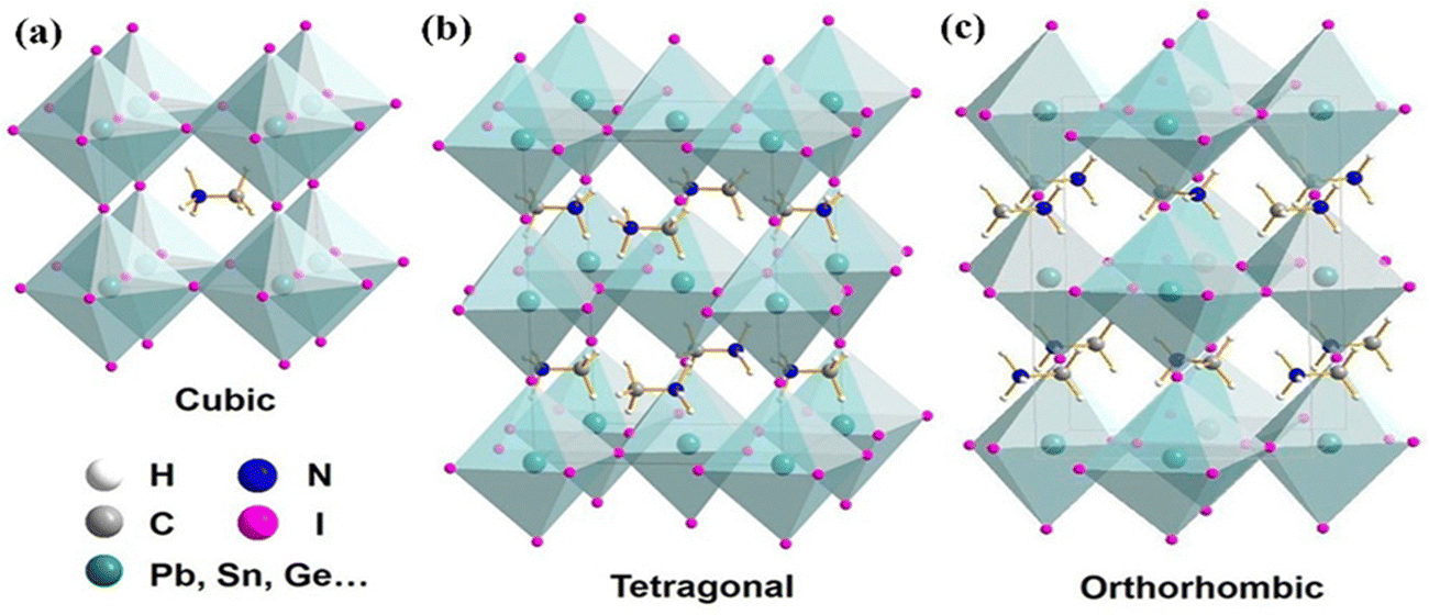 | ||
| Fig. 25 Different phases of MASnI3: (a) cubic, (b) tetragonal, and (c) orthorhombic. Reproduced with permission.271 Copyright 2017, American Chemical Society. | ||
Key properties of MASnI3 include:
• Optical band gap: approximately 1.3 eV.272
• Low carrier concentration: about 1 × 1014 cm−3.272
• Good electron mobility: around 2000 cm2 V−1 s−1.273–275
• Bulk electrical conductivity: approximately 5 × 10⁻² S cm−1.272
• Seebeck coefficient: around 260 mV K−1.272
• Room temperature behaviour: exhibits n-type behaviour.
Additionally, intermediate perovskites, like MASn1−xPbxI3, with increasing Sn content, exhibit superior optoelectronic performance compared to MAPbI3, with a band gap of approximately 1.17 eV, high carrier concentration of about 7.94 × 1014 cm−3, and large carrier mobility of around 2320 cm2 V−1 s−1. MASn0.5Pb0.5I3, among various compositions, has demonstrated the best-reported PCE of approximately 14.35%, making it highly promising for energy conversion and detector devices. Furthermore, the PV output of MASn0.5Pb0.5I3 can be influenced by its crystal symmetry and phase selection, leading to improved band gaps and economic viability compared to pure Pb-based perovskites.276,277
Enhancing the film quality and ensuring air stability is crucial for maximizing the PV performance of MASnI3. Several fabrication techniques, including co-evaporation, sequential evaporation, and the low-temperature vapor-assisted solution process (LT-VASP), have been developed to address these challenges. SnF2 doping in MASnI3 films increases the fluorescence lifetime and allows the fabrication of planar structure devices without needing a mesoporous electron-selective layer. Integrating different halogens into MASnX3 enables tuning the band gaps and allows control over the nucleation and growth processes, leading to an enhanced device FF. Nevertheless, there is a need to address obstacles concerning the resistance within the active and interfacial layers, as well as the electrode and contact, to enhance device performance and ensure a seamless integration with other substances. MASnI3-based PSCs are susceptible to the self-doping levels of MASnI3.276,278 The cubic unit cell of a-phase MASnI3 has a lattice parameter ranging from 6.231 to 6.243 Å.
The solid-state method or HI solution preparation method can be utilized to fabricate MASnI3 materials, leading to variations in properties; in particular, incorporating different halides can adjust the bandgap, yielding energies ranging from 1.30 to 2.15 eV. Excellent crystallinity is exhibited by MASnX3 films processed through solution methods. An estimated hole diffusion length of around 193 ± 46 nm was found for MASnI3, while the electron-diffusion length was approximately 279 ± 88 nm.272,279
3.2.1.2. FASnI3. In recent years, FASnI3, a variant of the perovskite material MASnI3, has garnered significant attention in photovoltaics. FASnI3 possesses a relatively low band gap of approximately 1.41 eV, making it an attractive candidate for solar cell applications.280 The rigid perovskite structure, resulting from strengthened hydrogen bonding between the larger-sized HC(NH2)2+ cations and the Sn2+ matrix, contributes to enhanced temperature stability and film quality. Fig. 26 displays the unit cells with the cubic α phase, tetragonal β phase, and tetragonal γ phase. Unlike MASnI3, FASnI3 remains a single phase at room temperature and exhibits a high phase transition at high temperatures.
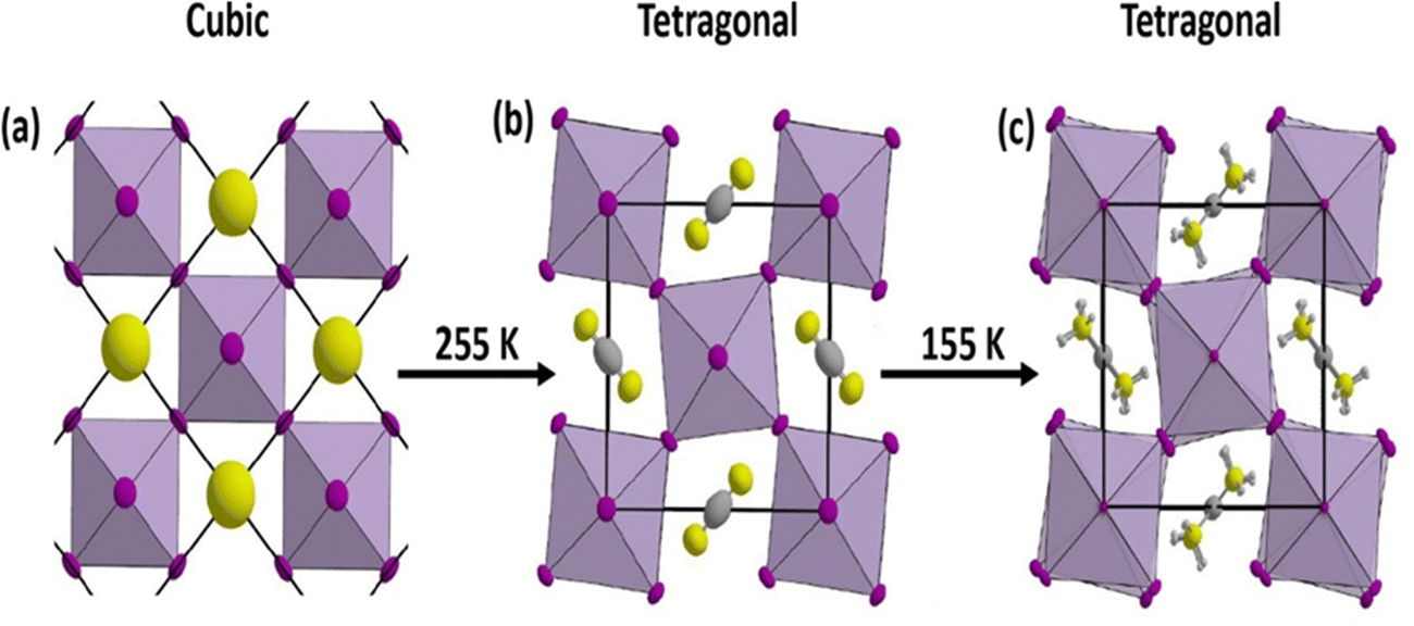 | ||
| Fig. 26 Transformation of FASnI3 from (a) cubic α phase at room temperature into (b) tetragonal β phase and, after that, into (c) tetragonal γ phase. Reproduced with permission.281 Copyright 2020, American Chemical Society. | ||
The performance of FASnI3-based solar cells has been significantly improved through various optimization strategies. For instance, adding SnF2 to FASnI3 films led to an enhanced PCE of approximately 2.10%.282 Further advancements have been achieved by incorporating SnF2–pyrazine complex additives, which promote the growth of smooth and compact films without phase separation. These optimized films have exhibited reduced charge recombination, resulting in a high efficiency of approximately 4.8% without hysteresis behaviour.283–286 Recent research has resulted in the development of dense, uniform, and full-coverage FASnI3 films by combining a simple inverted device architecture with SnF2-diethyl ether additives. A narrow band gap of around 1.40 eV was achieved by these films, achieving the highest reported PCE of about 14%.287 The inverted device architecture, along with the incorporation of fullerene, minimized the hysteresis behaviour and demonstrated good long-term illumination stability under continuous illumination. Adding FA cations to Sn-based PSCs has proven beneficial for enhancing the performance. FA cations alleviate the tendency of Sn2+ oxidation and enable the formation of mixed-cation perovskites with a narrow band gap of approximately 1.33 eV.
Due to the low controllability of perovskite film growth and the inherent ease of oxidation of Sn2+, Sn PSCs have been found to be significantly less efficient and stable than their Pb counterparts. Two pyridyl-substituted fulleropyrrolidines (PPF) were synthesized by Chen et al. in the cis (CPPF) and trans (TPPF) configurations and were employed as precursor additives. The electron density distributions and interactions with perovskite components were found to be significantly influenced by the spatial arrangements of the CPPF and TPPF. In comparison to the CPPF, the TPPF featured spatially separated pyridine groups that could capture more perovskite colloids via coordination bonds, thereby slowing down the perovskite crystallization process. Furthermore, the crystal orientation and film quality were enhanced. The TPPF was mostly located at the grain boundaries, aiding in the improvement of the interfacial energy-level alignment by suppressing the oxidation of Sn2+. Consequently, an excellent PCE of 15.38% (certified 15.14%) was exhibited by the TPPF-configured Sn PSC, with 99% and 93% of the initial PCE being maintained after 3000 h of storage and 500 h of constant irradiance, respectively.288 Moreover, the application of FASnI3-based perovskites extends beyond single-junction solar cells. A highly efficient four-terminal all-perovskite tandem solar cell, based on FASnI3 perovskite as the rear junction, achieved a significant milestone, with a PCE of approximately 19.08%. Similarly, FA Sn0.5Pb0.5I3 and FA0.75Cs0.25Sn0.5Pb0.5I3 PSCs have achieved impressive PCEs of approximately 10.9% and 14.1%, respectively. Notably, these perovskites can be employed as rear junctions in solution-processed tandem solar cells, eliminating the need for high-temperature thermal processing.289–295
Research has also investigated the stability of FASnI3-based perovskites. The incorporation of FA and Br into Pb- and Sn-based perovskites enables their band gaps to be tuned and their stability in the air to be enhanced. FASnI3 has been found to exhibit similar thermal stability but lower conductivity compared to MASnI3. Its growth conditions can be adjusted to achieve a range of conductivities, from p-type to intrinsic conductivity, while MASnI3 predominantly demonstrates p-type conductivity. The large ionic size of the FA cation contributes to an increased formation energy for Sn vacancies, resulting in improved charge-carrier mobility. FASnI3 has emerged as a promising absorber material for Sn-based PSCs due to its reduced bimolecular recombination and lower Auger rate than lead perovskites.296 Furthermore, inverted FASnI3-based PSCs have demonstrated superiority over MASnI3-based PSCs, leading to improved device performance. Innovative growth methods and improved tolerance to oxygen make FASnI3 a viable option for stable and efficient solar cell applications.297–300 FASnI3 offers numerous advantages over other perovskite materials, making it an attractive candidate for photovoltaic applications. Its low band gap, enhanced stability, and optimized film quality have contributed to the development of high-efficiency solar cells. Substantial improvements have been observed in the PCE of FASnI3-based solar cells due to various optimization strategies and innovative device architectures. Great promise is held for the future of solar energy conversion by FASnI3-based perovskites, supported by ongoing research and advancements.301
3.2.2.1. CsSnI3. The distinctive characteristics and potential for advanced applications have led to considerable interest in CsSnI3 perovskite materials within the realm of solar cell investigations. These perovskites come in multiple forms, such as a one-dimensional dual-chain structure with a yellow colour, a three-dimensional black perovskite configuration, and cubic black perovskite phases. CsSnI3 takes on a deformed three-dimensional perovskite arrangement characterized by orthorhombic symmetry at ambient temperature.302–305 This substance is categorized as a p-type element, displaying a moderately low density of carriers. The semiconductor capabilities of the black orthorhombic perovskite configuration of CsSnI3, with a direct bandgap, can be utilized in applications, whereby light emission upon excitation and electrical conductivity both increase with rising temperature. CsSnI3 also exhibits similar diffusion distances when compared to perovskite materials containing Pb. The number of carriers and the conductive properties of CsSnI3 are contingent on the vacancies of Sn, I, and Cs within its structure.306–311
CsSnI3 perovskites exhibit similar optical and electrical properties to FASnI3, another popular perovskite material, but boast better thermal stability.312,313 The three-dimensional perovskite building blocks of CsSnI3 are shown in Fig. 27. Initially, they were employed as materials for transporting holes in dye-sensitized solar cells because of their significant p-type characteristic and excellent hole mobility. CsSnI3's ideal bandgap of 1.3 eV makes it intriguing for use in single-junction solar cells.314–316 Substituting halides enables the tuning of the bandgap of CsSnI3, leading to a variation from 1.3 to 1.7 eV for CsSnBr3, accompanied by a change in the crystal structure from orthorhombic to cubic.313,317 QDs of CsSnI3 have achieved promising results, with a PCE of 5.03% and excellent stability over 90 days.318 To enhance the performance of all-inorganic Sn-halide PSCs, defect passivation additives, such as thiosemicarbazide, have been utilized, resulting in a high PCE of 8.20%319 CsSnI3 PSCs have shown considerable potential, with reported PCE values of 0.9% to 8.20%, depending on various factors, such as composition engineering, device architecture, and surface passivation strategies.
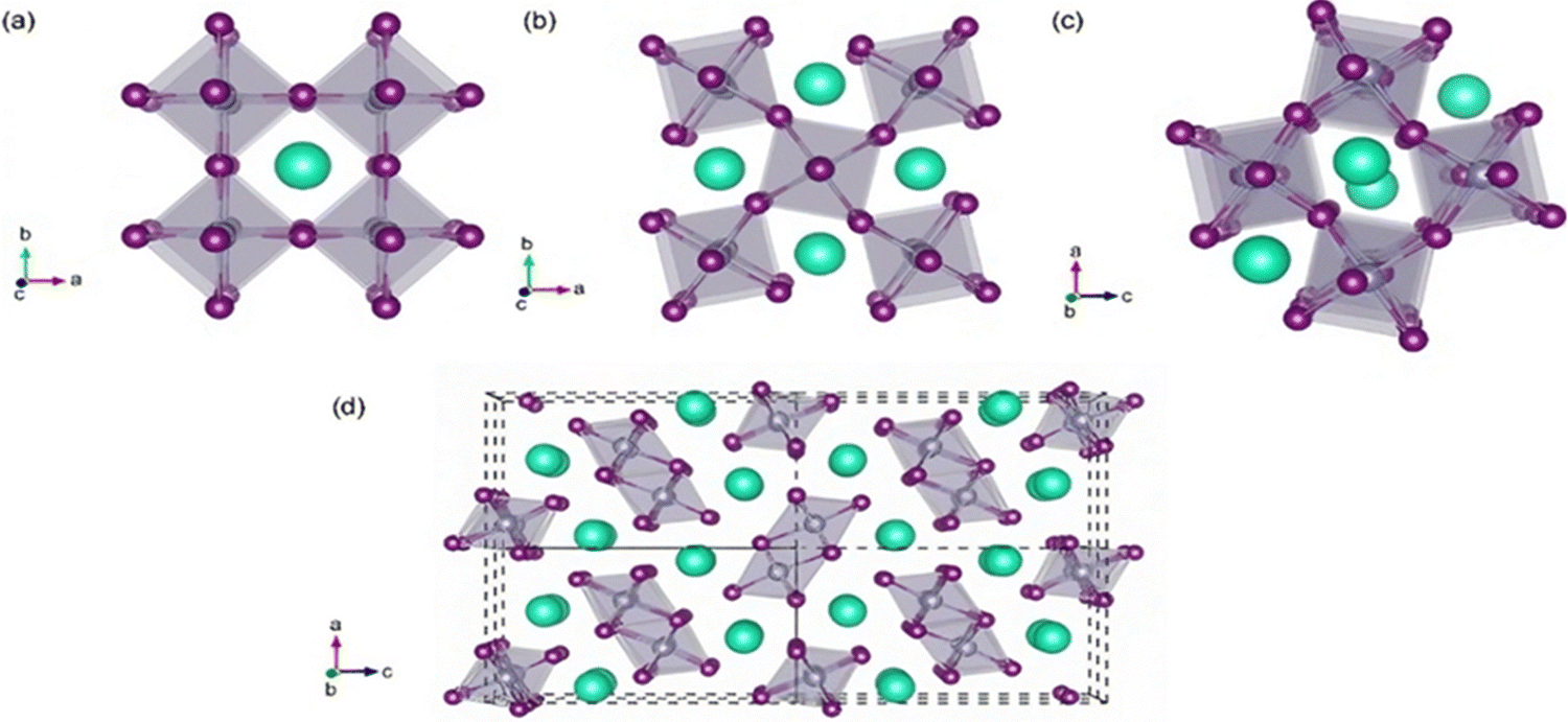 | ||
| Fig. 27 One-dimensional images showing the (a) α phase in the cubic form, (b) β phase in the tetragonal form, (c) γ phase in the orthorhombic form, and (d) Sn halide octahedral networks, all broken down into one-dimensional chains in each image, the green spheres depict Cs atoms, while the purple polyhedra represent the octahedral perovskite cage formed by bonding Sn in steel blue and I in dark purple atoms. Reproduced with permission.320 Copyright 2015, American Physical Society. | ||
Studies have demonstrated that the introduction of additives, including Sn halides, like SnF2, SnCl2, SnI2, and SnBr2, can improve film quality and enhance the performance of CsSn (I, Br)3 PSCs. For instance, CsSnI3 films with added SnCl2 exhibited the highest pinhole density, and devices without a hole-transporting layer achieved the highest FF and PCE. Moreover, doping CsSnI3 with Br resulted in CsSnI3−xBrx perovskites, which exhibited higher FF values compared to pure CsSnI3.321 While all-organic CsSnI3 shows possible application in inverted PSCs due to its outstanding air and thermal stability,312,313 research efforts continue to explore different approaches to improve the stability and performance of CsSnI3-based photovoltaic devices. These include localized electron density engineering, surface passivation strategies, and optimization of the device architectures. Research and development in the pursuit of high-efficiency and stable CsSnI3 PSCs continues to be actively pursued. Table 14 provides a comparative analysis of lead-free perovskite device structures, presenting their corresponding solar cell parameters to understand their performance comprehensively.
| Light absorber | Architecture | V oc [V] | J sc [mA cm−2] | FF [%] | PCE [%] | Ref. |
|---|---|---|---|---|---|---|
| MASnI3 | FTO/c-TiO2/mp-TiO2/MASnI3/spiro-OMeTAD/Au | 0.88 | 16.8 | 0.42 | 6.4 | 269 |
| MASnI3 | FTO/c-TiO2/MASnI3/spiro-OMeTAD/Au | 0.716 | 15.18 | 0.50 | 5.44 | 322 |
| MASnBr3 | FTO/c-TiO2/mp-TiO2/MASnBr3/spiro-OMeTAD/Au | 0.88 | 8.26 | 0.59 | 4.27 | 323 |
| MASnI3 | FTO/c-TiO2/mp-TiO2/MASnI3/PTAA/Au | 0.27 | 17.4 | 0.39 | 1.86 | 324 |
| MASnIBr2 | FTO/c-TiO2/mp-TiO2/MASnIBr2/spiro-OMeTAD/Au | 0.82 | 12.33 | 0.57 | 5.73 | 323 |
| MASnBr3 | FTO/c-TiO2/mp-TiO2 MASnBr3/P3HT/Au | 0.50 | 4.27 | 0.49 | 1.12 | 325 |
| MASnBr3 | ITO/PEDOT:PSS/MASnBr3/PCBM/Bis-C60/Ag | 0.20 | 4.5 | 0.36 | 0.3 | 326 |
| FASnI3 | ITO/PEDOT:PSS/FASnI3/C60/BCP/Ag | 0.92 | 20.4 | 76.7 | 14.3 | 287 |
| FASnI3 | ITO/PEDOT:PSS/FASnI3/C60/BCP/Ag | 0.31 | 18.36 | 0.67 | 3.85 | 252 |
| FASnI3 | ITO/PEDOT:PSS/FASnI3/C60/BCP/Ag | 0.36 | 17.6 | 0.62 | 4.0 | 327 |
| CsSnI3 | FTO/c-TiO2/mp-TiO2/CsSnI3/spiro-OMeTAD/Au | 0.52 | 10.21 | 0.65 | 3.31 | 328 |
| CsSnI3 | ITO/PEDOT:PSS/CsSnI3/PC61BM/BCP/Ag | 0.53 | 20.5 | 60.1 | 6.53 | 329 |
3.2.3.1. Cs2SnI6. Cs2SnI6 belongs to the 〈111〉-oriented perovskite family, resulting from the cubic 3D structure of CsSnI3, as shown in Fig. 28. Its crystallographic characteristics encompass a zero-dimensional configuration featuring distinct molecular [SnI6]2− octahedra.330,331 Within this arrangement, half of the Sn atoms within the octahedral structure at the B site remain unoccupied. This arrangement, resembling a molecular salt, exhibits a relatively ionic character, with Cs atoms occupying the spaces between the [SnX6] octahedra. The material's intrinsic resistance to oxidation and greater environmental stability are attributed to the presence of the Sn4+ state and strong Sn–I covalent bonds,331–333 leading to a smaller Sn–I bond length (2.85 Å) compared to CsSnI3 (3.11 Å) due to structural relaxation.277
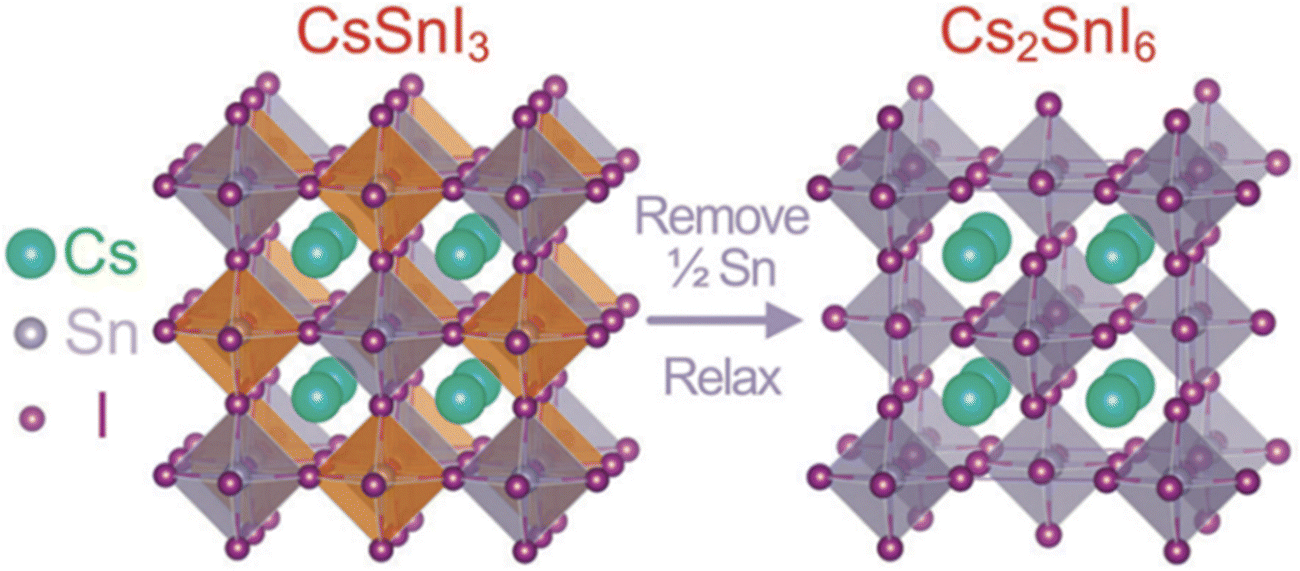 | ||
| Fig. 28 Cs2SnI6 crystal structure derived from CsSnI3. Reproduced with permission.258 Copyright 2015, Royal Society of Chemistry. | ||
The increased durability of Cs2SnI6 compared to CsSnI3 has been validated by density functional theory (DFT) computations. Furthermore, Cs2SnI6 displays ambipolar characteristics, enabling it to undergo p-type or n-type semiconductor doping. Additionally, it showcases a finely tuned bandgap Eg spanning from 1.27 to 1.62 eV, rendering it a viable option for applications in photovoltaics.334,335 The material's high absorption coefficients and carrier mobility further highlight its potential for photovoltaics. The dual nature of Cs2SnI6 is due to the creation of p-type vacancies in the caesium or n-type vacancies/interstitial Sn in the iodide. Fig. 29 shows the band structure of Cs2SnI6, with an unmediated bandgap at the Γ juncture of around 1.3 eV, albeit minor disparities exist between the experimentally determined and theoretically projected bandgap values.321,336,337
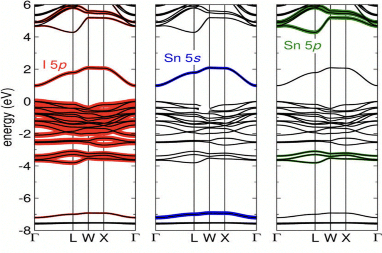 | ||
| Fig. 29 Band structure of Cs2SnI6. Reproduced with permission.338 Copyright 2016, American Chemical Society. | ||
Cs2SnI6 has shown great promise as a light-absorbing material for solar cells. Its favourable characteristics, including proximity to the Shockley–Queisser limit, suitable bandgap, and stability, have garnered significant research attention. Efforts to enhance its efficiency have been made by optimizing the device structure. For instance, Cs2SnI6 PSCs with c-TiO2 and P3HT as the ETL and hole transport layer (HTL), respectively, resulted in a PCE of 0.96% and a Voc of 0.51 V, mainly through optimization of the perovskite layer thickness.339 Nevertheless, the effectiveness of Cs2SnI6 photovoltaic cells is impacted by the energy level disparity at the ETL/perovskite/HTL interfaces. This disparity results in a suboptimal extraction of electrons and holes, thereby resulting in the comparatively modest efficiency of the device. Under ambient conditions, the stability of Cs2SnI6 is considered significant, with Cs2SnI6 films showing fairly good stability for at least one week. However, the challenge of maintaining long-term stability in Cs2SnI6 PSCs remains. The degradation of Cs2SnI6 PSCs begins after one week of air exposure, and they tend to fail after one month of humidity exposure. To overcome this limitation, various materials, including the choice of the HTL, are being explored by researchers to enhance the stability and device efficiency of Cs2SnI6 in PSCs.340 Despite the challenges faced in achieving high efficiency, Cs2SnI6 is still considered to have potential as a light-absorbing material for solar cells. A promising PCE of 0.86% was achieved in one study using a configuration with FTO/ZnO compact-layer/nanorods/perovskite/P3HT/Ag.341 Improvement in device performance was achieved by effectively suppressing charge recombination through the optimization of the surface morphology of the ZnO seed layer. Furthermore, the utilization of Cs2SnI6 in planar solar cells resulted in the attainment of a PCE of 0.46%.342
3.3. Methods to improve the overall performance of Sn PSCs
Apart from the use of cationic Sn in the perovskite mentioned above, researchers have developed different additive manufacturing methods to further enhance the performance of these perovskites, as discussed below.3.3.1.1. Mixed cations. Perovskites based on mixed cations containing Sn have emerged as materials holding promise for the development of efficient and stable PSCs. Enhanced stability and PCEs have been exhibited by metal halide perovskites that initially explored mixed cations in Pb-based PSCs. However, previous attempts with the mixed cations MA and Cs yielded suboptimal PCEs, primarily due to the poor Voc.352–356 In this context, Zhao et al. investigated the influence of the mixed cations MA and FA on Sn-based perovskites. Their study revealed that the ratios of mixed cations strongly affected the optical properties of the perovskite materials. The introduction of the FA cation led to a blue-shifted emission of MASnI3, indicating the tunability of the electronic structure. Control of the bandgap within the range of 1.26 to 1.36 eV for (FA)x (MA)1−xSnI3 was achievable, with wider bandgaps produced by a higher FA content.298 These mixed-cation perovskites demonstrated reduced charge-carrier recombination, improved film morphology, and enhanced photovoltaic performance. Notably, the (FA)0.75 (MA)0.25SnI3 perovskite, doped with 10 mol% SnF2, exhibited an impressive maximum PCE of 8.12%.298 The unpredictable dynamics of crystal formation of Sn perovskites result in low quality, poor orientation, and a high defect density. Jiang et al. used formamidine acetate (FAAc) and ammonium iodide (NH4I) instead of formamidinium iodide (FAI) to grow Sn-perovskite films. The triple reagent (FAAc + NH4I + SnI2) technique extended the reaction path for forming Sn-perovskite films. At room temperature, it hindered the formation of 3D perovskite structures but had no effect on the low-dimensional structures. The low-dimensional structure generated at ambient temperature acted as a seed for 3D structure formation during further annealing processes. This triple reactant source produced a Sn-perovskite layer with improved orientation and long carrier lifetimes, resulting in a 14.6% efficiency for ITO/poly(3,4-ethylene dioxythiophene)/poly(styrene sulfonate) PEDOT/PSS/Sn- perovskite/indene-C60-bis-adduct (ICBA)/bathocuproine (BCP)/Ag perovskite solar cells.357Table 15 summarises the performance of this mixed cations and the respective solar cell parameters.
| Light absorber | Architecture | V oc [V] | J sc [mA cm−2] | FF [%] | PCE [%] | Ref. |
|---|---|---|---|---|---|---|
| FAAc + NH4I + SnI2 | ITO/PEDOT:PSS/FA0.75MA0.25SnI3/ICBA/BCP/Ag | 0.96 | 20.47 | 74.5 | 14.6 | 357 |
| Cs0.1FA0.9SnI3 | FTO/c-TiO2/mTiO2/perovskite/ThMAI/PTAA/Au | 0.521 | 24.12 | 72.02 | 9.06 | 358 |
| FA0.75MA0.25SnI3 | ITO/PEDOT:PSS/FA0.75MA0.25SnI3/PC61BM/BCP/Ag | 0.55 | 19.4 | 67 | 7.2 | 359 |
| FA0.75MA0.25SnI3 | ITO/PEDOT:PSS/FA0.75MA0.25SnI3/PC61BM/BCP/Ag | 0.55 | 20 | 65 | 7.1 | 359 |
| FA0.75MA0.25SnI3 | ITO/PEDOT:PSS/FA0.75MA0.25SnI3/PC61BM/BCP/Ag | 0.53 | 20.4 | 64 | 6.9 | 359 |
| FA0.75MA0.25SnI3 | ITO/PEDOT:PSS/FA0.75MA0.25SnI3/PC61BM/BCP/Ag | 0.54 | 17.2 | 61 | 5.7 | 359 |
| (FA)0.50(MA)0.50SnI3 | ITO/PEDOT:PSS/(FA)0.50(MA)0.50SnI3/PC61BM/BCP/Ag | 0.53 | 21.3 | 52.4 | 5.92 | 360 |
| (FA)0.25(MA)0.75SnI3 | ITO/PEDOT:PSS/(FA)0.25(MA)0.75SnI3/PC61BM/BCP/Ag | 0.48 | 20.7 | 45.2 | 4.49 | 360 |
| Perovskite + additive | Structure of the device | V oc [V] | J sc [mA cm−2] | FF [%] | PCE [%] | Ref. |
|---|---|---|---|---|---|---|
| MASnI3 + SnF2 | FTO/c-TiO2/mp-TiO2/absorber/Au | 0.32 | 21.4 | 0.46 | 3.15 | 361 |
| MASnI3 + hydrazine vapour | FTO/c-TiO2/mp-TiO2/absorber/PTAA/Au | 0.38 | 19.9 | 0.51 | 3.80 | 362 |
| MASnIBr2−xClx + 0% SnCl2 + 100% SnBr2 | Glass/FTO/TiO2/absorber/carbon | 0.31 | 13.37 | 0.52 | 2.18 | 147 |
| MASnI3 + SnF2 | FTO/PEDOT:PSS/absorber/C60/BCP/Ag | 0.45 | 11.8 | 0.40 | 2.14 | 363 |
| en[MASnI3] + SnF2 | FTO/c-TiO2/mp-TiO2/absorber/PTAA/Au | 0.43 | 24.3 | 0.63 | 6.63 | 364 |
| MASnI3 + SnF2 | ITO/PEDOT:PSS/absorber/C60/BCP/Ag | 0.46 | 21.4 | 0.42 | 4.29 | 365 |
| MASnI3 | ITO/PEDOT:PSS/poly-TPD/absorber/C60/BCP/Ag | 0.38 | 12.1 | 0.36 | 1.7 | 366 |
| FASnI3 + SnF2 pyrazine | FTO/c-TiO2/mp-TiO2/absorber/spiro-OMeTAD/Au | 0.32 | 23.7 | 0.63 | 4.8 | 56 |
| FASnI3 + 50% PEAI | ITO/PEDOT:PSS/absorber/C60/BCP/Ag | 0.38 | 19.96 | 0.69 | 5.28 | 114 |
| FASnI3 + SnF2 | FTO/c-TiO2/mp-TiO2/ZnS/absorber/PTAA/Au | 0.38 | 23.1 | 0.60 | 5.27 | 75 |
| FASnI3 + LiF | ITO/PEDOT:PSS/absorber/C60/BCP/Ag | 0.38 | 19.65 | 0.71 | 5.04 | 367 |
| FASnI3 + SnF2 | FTO/c-TiO2/mp-TiO2/ZnS/absorber/PTAA/Au | 0.38 | 23.1 | 0.60 | 5.27 | 75 |
| FASnI3 + LiF | ITO/PEDOT:PSS/absorber/C60/BCP/Ag | 0.38 | 19.65 | 0.71 | 5.04 | 367 |
| FASnI3 + SnF2 | FTO/c-TiO2/mp-TiO2/ZnS/absorber/PTAA/Au | 0.38 | 23.1 | 0.60 | 5.27 | 75 |
| FASnI3 + diethyl ether | ITO/PEDOT:PSS/absorber/C60/BCP/Ag | 0.47 | 22.1 | 0.60 | 6.22 | 368 |
| FASnI3 + SnF2 | ITO/PEDOT:PSS/absorber/C60/BCP/Ag | 0.48 | 21.3 | 0.64 | 6.6 | 365 |
| FASnI3 + LiF | ITO/PEDOT:PSS/absorber/C60/BCP/Ag | 0.38 | 19.65 | 0.71 | 5.04 | 367 |
| CsSnI3 + SnF2 | FTO/TiO2/CsSnI3/m-MTDATA/Au | 0.24 | 22.70 | 37.0 | 2.02 | 369 |
| FASnI3 + EVA | ITO/PEDOT:PSS/absorber/C60/BCP/Ag | 0.523 | 22.80 | 64.7 | 7.72 | 141 |
| CsFASnI3 + SnF2, SnCl2 | FTO/PEDOT:PSS/CsFASnI3/PTAA/Au | 0.64 | 22.2 | 70.8 | 10.08 | 121 |
| FASnI3 + trimethylthiourea | ITO/PEDOT:PSS/absorber/C60/BCP/Ag | 0.9 | 21 | 75.69 | 14.06 | 61 |
3.3.2.1. Antioxidants. Antioxidant additives are pivotal for enhancing the efficiency and long-term stability of Sn perovskite solar cells, as they shield Sn2+ from oxidation in ambient conditions. An array of additives, such as divalent Sn halides and hydrazine derivatives, have been incorporated to counteract this oxidation phenomenon. One notably influential group of additives among these is represented by Sn double halides, which are characterized by serving dual roles as antioxidants and Sn sources, thereby ensuring the protection of perovskite films. Mathews et al.370 showcased the utilization of SnF2 to diminish intrinsic Sn-cation vacancies in CsSnI3 perovskites, and reported it could lower the carrier density and enhance the conductivity. The integration of 20 mol% SnF2 resulted in a notable 2.02% efficiency, accompanied by an elevated current density and extended spectral response.
Similarly, Yan et al.371 integrated SnF2 into FASnI3 films, effectively diminishing the carrier density and achieving a commendable efficiency of 6.22%. Hatton et al.372 compared the efficacy of four SnX2 additives (SnF2, SnCl2, SnBr2, and SnI2), and observed superior stability in SnCl2, which acted as a barrier layer, effectively preventing the intrusion of oxygen and moisture. Further studies373 showed that when SnF2 and SnCl2 were combined, they formed a protective layer with both amorphous and polycrystalline characteristics on the surface of perovskite films, effectively boosting the stability. This protective layer was confirmed through grazing incident X-ray diffraction (GIXRD) and high-resolution transmission electron microscopy (HRTEM). As a result, the PSCs exhibited remarkable stability, experiencing minimal performance degradation even over prolonged operational periods.
3.3.2.2. Co-additives. The use of co-additives can be instrumental in enhancing the stability and performance of Sn perovskite solar cells by addressing the phase segregation problems induced by surplus SnX2 salts. These additives interact with SnX2 to create complexes, impeding phase separation and ensuring the uniform encapsulation of Sn perovskite grains. Pyrazine, renowned for its formidable binding affinity, is often engaged in the formation of complexes with SnF2, resulting in the effective eradication of micrometre-sized aggregations on perovskite surfaces, thereby enhancing stability. Similarly, Wang et al.374 employed HPA to mitigate phase separation in CsSnIBr2 perovskite films, thereby effectively decreasing the carrier density and improving the thermal stability. Small molecules containing electronegative heteroatoms, such as piperazine, 8-hydroxyquinoline, and trimethylamine, were developed by them to enhance both the efficiency and stability. Co-additives were also employed to alleviate the phase segregation of SnCl2. Yan et al.375 investigated hydroxybenzene sulfonic acid or salt to establish a robust coordination with SnCl2 for impeding phase separation and enhancing stability. Furthermore, additives such as ammonium hypophosphite (AHP) and gallic acid (GA) were incorporated to improve efficiency and stability. In particular, GA facilitated the formation of a SnCl2–GA antioxidant layer, resulting in a record PCE of 9.03% for FASnI3-based PSCs that also demonstrated exceptional stability exceeding 1000 h without encapsulation.
3.3.2.3. Hydrazine derivatives. Hydrazine derivatives, well-known for their potent reducing properties, have emerged as effective antioxidant agents for ASnX3 perovskites. The pioneering work of Kanatzidis et al.376 utilized hydrazine vapour (N2H4) treatment to prevent Sn2+ oxidation during Sn perovskite film fabrication. The vapour reacted with SnI62− components, reducing Sn4+ to Sn2+, thereby improving film conductivity. This treatment resulted in efficiencies of 3.89%, 1.83%, and 3.04% for MASnI3, CsSnI3, and CsSnBr3, respectively. Similarly, hydrazine vapour treatment-modified CsSnI3 films achieved a champion efficiency of 4.81%.377 Jiang et al. utilized trihydrazine dihydroiodide (THDH) to fabricate an efficient FASnI3-based solar cell, yielding a maximum efficiency of 8.48%.378 Hydrazinium halide salts, which is hydrazinium iodide (HAI), offers improved stability too. Tsarev et al.379 employed HAI as an additive, resulting in high-quality MASnI3 films with enhanced photostability.
3.3.2.4. Alkali cations. To tackle the challenges of poor crystallinity and phase instability in FASnI3 perovskites, Wu et al.380 introduced a structural regulation strategy involving Cs doping. Incorporating Cs reduced lattice distortion, thereby giving the cubic structure rather than orthorhombic. This transition enhanced the UV-vis light absorption and crystalline degree, consequently improving the thermodynamic stability. As a result, there was a significant efficiency boost, reaching 6.08% with 8 mol% CsI. Similarly, Miyano et al.381 investigated Rb doping in FASnI3 perovskite, and found it reduced the optical bandgap and trap density. Incorporating 8 mol% Rb resulted in high-coverage Sn perovskite films and improved the device efficiency by approximately 80% compared to pristine FASnI3-based devices, achieving a PCE of 5.89%.
3.3.2.5. Large-sized monovalent organic ammonium. Optimizing the crystal orientation and facilitating the formation of 2D or quasi-2D perovskite structures could be achieved by incorporating large-sized monovalent organic ammonium into the Sn perovskite lattice. This enhanced the resistance to oxygen and moisture and acted as a passivation agent, thereby increasing the Voc of Sn PSCs. For example, research conducted by Kanatzidis et al. demonstrated the crystallographic and photoelectric properties of (BA)2(MA)n−1SnnI3n+1 perovskites,382 resulting in an efficiency improvement of 5.94% for Sn PSCs. The unstable nature of Sn perovskite solar cells in the presence of oxygen has hampered their technological development to date. To address this issue, Liao et al. reported (PEA)2FA8Sn9I28, a low-dimensional Sn perovskite with significantly higher air stability than its 3D counterparts. The reduced degradation during air exposure was due to its increased thermodynamic stability, through encapsulating organic ligands, and the compact perovskite coating that prevents oxygen entry. Further, the perpendicular development of perovskite domains between electrodes promotes effective charge-carrier transport, resulting in power conversion efficiencies of 5.94% without additional device structural engineering. Also over 100 hours, the unencapsulated devices revealed no significant decrease in efficiency.383 Moreover, Diau et al. utilized GA+ to partially replace FA+ in FASnI3 perovskite, resulting in an efficiency of 9.6% alongside durable moisture resistance.384 Additionally, HEA+ was employed to enlarge the unit cell of FASnI3 perovskite, thereby enhancing the lattice symmetry. 5-AVA+ could cross-link Sn perovskite crystals via hydrogen bonding, decelerating the crystallization rates and improving the film quality and stability.385 Co-doping with NH4Cl produced highly vertically oriented perovskite films, resulting in a PCE of 8.71% for Sn PSCs. Fluorine-functionalized cations, like 2-F-PEA+ and FOE+, can passivate FASnI3 perovskite surfaces, diminishing the trap density and optimizing crystal alignment, resulting in a certified steady-state efficiency of 10.16% for Sn PSCs.386,387
3.3.2.6. Large-sized divalent organic ammonium. Diau et al. demonstrated that 1
mol% EDAI2 doping in FASnI3 perovskite could yield a pinhole-free morphology and increase the Voc of Sn PSCs from 0.360 to 0.516V. In addition, storage time induced lattice relaxation, prolonging the carrier lifetime and increasing the efficiency to 8.9% after 1462h.388 Sn perovskite films doped with PN2+ and TN2+ showed an increased coverage ratio and widened optical bandgap, thereby enhancing the device efficiency. TN-doped FASnI3 exhibited higher efficiency due to the more significant blue shift in the photoluminescence peak. BEA2+ incorporation formed a Dion–Jacobson (DJ) phase 2D Sn perovskite, enhancing the structural stability and carrier diffusion length. Sn PSCs based on (BEA)FAn–1SnnI3n+1 perovskite achieved high efficiency and stability.389 Padture et al. revealed that 4AMP2+ integration could form a DJ-phase 2D Sn perovskite with enhanced interlayer bonding and a longer carrier recombination lifetime. The optimized 4AMP2+ doping concentration yielded a high-efficiency Sn PSC with a Voc of 0.69V.390,391 Although the ideal bandgap and eco-friendliness of Sn perovskites are very promising for PSCs, the short carrier diffusion length and high defect density in nominally synthesized films restrict its application. Consequently, Li et al. showed that Sn-based perovskite films with high-member low-dimensional Ruddlesden–Popper (RP) phases and a favoured crystal orientation distribution could achieve extended carrier diffusion lengths. The film's synthesis relied on a molecular additive composed of phenylethylammonium cations and ideally blended halide-pseudo-halide anions. This additive could optimize the quasi-2D crystallization kinetics of Sn-based perovskites. The high-member RP film structure improved the Jsc and increased the PCE to 14.6%. The ITO/PEDOT/Perovskite/ICBA/BCP/Ag device exhibited near-unity shelf stability after 1000 h in nitrogen. A sample of 50 devices demonstrated remarkable reproducibility, with PCEs ranging from 13.0% to 14.6%.392
3.3.2.7. Lewis adduct and hydrogen bonding. Additives that induce further chemical interactions with Sn halide precursors, such as Lewis acid–base interactions and hydrogen bonding, have shown promise for reduction of the crystallization rates and the passivation of surface trap states in Sn perovskite films. For example, modulation of the crystallization rate of MASnI3 perovskite was achieved by Kanatzidis et al. through the use of DMSO, leading to the formation of uniform and pinhole-free MASnI3 films after annealing, accompanied by the attainment of an efficiency of 3.15% and a remarkable Jsc of 21.4
mA cm−2.393 Chen et al. reported the use of poly(ethylene-co-vinyl acetate) (EVA) as an additive to control the nucleation and orientation of FASnI3 perovskite, leading to a 47.6% increase in device PCE.394 Ning et al. used ammonium thiocyanate (NH4SCN) as an additive to regulate the growth dynamics of quasi-2D intermediate phases in Sn perovskite films, resulting in improved stability.395 Triphenylamine-based Lewis base additives were studied for their effects on FASnI3 perovskite film crystallization dynamics, with CDTA enabling a significant enhancement in device PCE.396 Moreover, the addition of PVA with hydroxyl groups into a FASnI3 perovskite precursor led to an increase in Voc and operational stability under continuous illumination.397 Sn-halide perovskites use less regulated ingredients than Pb in conventional perovskite solar cells. However, even the best tin-halide perovskite thin films have a restricted carrier diffusion length and poor morphology. Jiang et al. developed a synthetic method to react metallic Sn and I2 in DMSO, resulting in a well-dispersed SnI2·(DMSO)x adduct in the precursor solution. The adduct promoted the out-of-plane crystal orientation, producing a more uniform structure in polycrystalline perovskite thin films. This method enhanced the electron-diffusion length of Sn-halide perovskite to 290 ± 20 nm, compared to 210 ± 20 nm in the reference films. An (ITO)–glass/PEDOT/tin-halide perovskite/indene-C60 bis-adduct (ICBA)/bathocuproine (BCP)/Ag PSC achieved a PCE of 14.6%, as validated by an independent lab. This represented an approximately 20% gain over the previous best-performing certified Sn-halide perovskite solar cells. The cells surpassed previous inorganic-active-layer-based thin-film solar cells, including those based on amorphous silicon, Cu2ZnSn(S/Se)4, and Sb2(S/Se)3.398
4. Disadvantages of using Sn in PSCs
Despite the numerous benefits associated with utilizing Sn in solar cells, Sn-based perovskite solar cells still face significant hurdles that must be addressed for their commercialization. As illustrated in Fig. 30, these drawbacks are evident. Below, we briefly discuss these disadvantages. | ||
| Fig. 30 Disadvantages of using Sn in the ETLs and absorber layers of MH-PSCs. | ||
4.1. Sn in the ETL layer
4.2. Sn in the absorber layer
4.3. Environmental concerns
The integration of Sn and SnO2 in perovskite solar cell technology brings forth critical considerations regarding both the environmental impact and toxicity, necessitating a comprehensive examination for informed decision-making. While lead-based perovskite cells have been shown to cause minimal environmental harm during the manufacturing stages, their tin-based counterparts present a contrasting scenario. The inherent attributes of tin-based cells, including their lower efficiency, heightened energy consumption in production, and increased material usage, collectively contribute to amplified environmental footprints, thereby underscoring the urgency of evaluating their sustainability from an ecological perspective.411–413Moreover, comparative analyses have revealed that tin-based perovskite cells manifest heightened terrestrial ecotoxicity and contribute more substantially to global warming than lead-based alternatives. These findings not only accentuate the environmental concerns associated with tin-based solar cell technologies but also underscore the imperative to address the potential long-term repercussions they may have on ecosystems and human health. The complexities surrounding the toxicity of Sn compounds further underscore the necessity for in-depth exploration. While SnO2 is generally perceived as less toxic than its lead-based counterparts, empirical evidence suggests nuanced toxicity concerns, particularly concerning exposure to certain Sn compounds. Studies highlight the heightened toxicity of Sn compounds like SnI2, attributing it to acidification effects, necessitating a nuanced understanding of their environmental impact. Additionally, adverse effects observed on plant life in response to exposure to Sn-based perovskites accentuate the necessity for comprehensive ecological assessments.414,415
Furthermore, the toxicity profile of SnO2 compounds warrants meticulous consideration, especially in occupational settings where exposure risks are pronounced. Chronic exposure to inorganic Sn compounds during processing may elicit respiratory and gastrointestinal symptoms, necessitating stringent safety protocols to safeguard human health and minimize environmental contamination.
5. Conclusion and future perspectives
As the landscape of SnO2-based PSCs continues to evolve, formidable challenges remain around their stability, scalability, and hysteresis mitigation, as well as optimizing the fabrication process for the duration and cost. This has created an arena ripe for further research and innovation, shaping a trajectory toward enhanced performance and expanded applicability. The realm of SnO2-based solar cells has already witnessed remarkable progress, marked by improved efficiencies and enhanced stability, but as we look ahead, several avenues for future advancements have emerged that can elevate the potential of SnO2-based solar cell technology. The following outlines some potential directions that research and innovation may take:The pursuit of higher efficiency and exceptional stability remains a cornerstone of future research endeavours. Advanced material engineering approaches, including controlled synthesis and optimization strategies, are pivotal pathways in this regard.
The refinement of SnO2 nanocrystal synthesis techniques holds promise for fine-tuning their essential attributes, such as band structure, size, and morphology. The aim is for the resulting high-quality SnO2 compact layers to foster enhanced light trapping and charge collection, ultimately improving overall cell performance.
Addressing the stability of SnO2-based solar cells is essential for realizing high reproducibility and extended device lifetimes.
Harnessing novel materials and coatings is important to safeguard SnO2 against degradation mechanisms, such as moisture and oxygen infiltration, which could significantly enhance device robustness.
Moreover, exploring advanced encapsulation techniques and developing efficient passivation layers may boost the cells' resistance to external stresses, opening new avenues for reliable long-term operation.
The translation of laboratory successes to practical applications hinges on scalable manufacturing methods. Therefore, investigating large-scale production techniques, such as roll-to-roll manufacturing and high-quality perovskite film deposition, is critical to facilitate the fabrication of cost-effective, high-performance solar modules.
These strategies can expedite the integration of SnO2-based solar cells into the mainstream energy landscape, enabling their widespread adoption. Using a carrier concentration-controlled SnO2 QD ETL presents a promising route to obtaining stable, efficient, reproducible, large-scale, and flexible planar solar cells. Exploring the potential of tandem solar cells, where SnO2-based materials can serve as a complementary component, offers the prospect of elevating overall energy-conversion efficiencies. This avenue necessitates an inclusive understanding of the intricate association between SnO2's structure and properties, driving accurate control of the SnO2 layers and thus promoting the holistic advancement of SnO2-based solar cells. The future of SnO2-based solar cells is full of exciting possibilities and challenges. As researchers delve deeper into synthesis techniques and manufacturing strategies, we are poised to witness breakthroughs that will redefine the landscape of renewable energy technology. By embracing the multidisciplinary nature of the field and fostering collaborative efforts, the vision of efficient, stable, and cost-effective SnO2-based solar cells can transition from a concept to a tangible reality, contributing significantly to the global pursuit of sustainable energy solutions.
The future of solar energy hinges on the development of efficient and sustainable photovoltaic technologies. There are some key directions in which further advancements could be helpful to bring this technology from the lab scale to use by society, as shown in Fig. 31. Among the promising alternatives to lead-based perovskite solar cells, Sn-based perovskites have emerged as frontrunner candidates. However, several challenges must be addressed to realize their full potential and enable their widespread adoption. By integrating innovative approaches and interdisciplinary collaborations, researchers aim to overcome these obstacles and unlock the remarkable capabilities of Sn-based perovskite solar cells. The main challenge for Sn-based perovskite solar cells is achieving a higher Voc. Despite achieving remarkable PCEs up to 9%, their Voc remains unacceptably low, limiting their overall performance. More basic research is needed to understand the origins of the low Voc, but focusing on enhancing both the Voc and FF simultaneously. A Voc higher than 1.0 V and an FF above 75% are critical targets to match the PCEs of Pb-based perovskite solar cells.
 | ||
| Fig. 31 Future prospects of Sn-based ETLs and absorber layers for MH-PSCs. This schematic shows a typical approach required to make Sn PSCs an alternate viable solar energy-harvesting technology. | ||
Another significant challenge is restraining the oxidation of Sn2+ ions and improving the air stability of Sn-based perovskite materials. Chemical composition and device engineering methods can help contain and control the instability issues, which would make Sn-based perovskites more commercially attractive and a viable option. Understanding whether the tendency of Sn-based halide perovskites to become hole-doped is intrinsic or extrinsic is crucial for overcoming this challenge and realizing their full potential.
Environmental impact and material stability: Sn-based perovskites, like their lead-based counterparts, can decompose upon exposure to water, releasing potentially toxic by-products. Efforts should focus on investigating the environmental impact of halide perovskite materials and developing innovative, stable, and low-toxicity alternatives. Further research is needed to understand the chemical and physical properties of Pb-free perovskite materials to fabricate improved devices and mitigate environmental concerns.
Beyond solar cells, future directions may explore applications such as LEDs, lasers, detectors, TFTs, and memory devices using Sn-based perovskites. Material discovery and physical studies, coupled with device engineering improvements, will enable Sn-based perovskites to realize their full potential in various applications. For materials with high “electronic” dimensionality, optimizing charge transport rather than just the physical structure will be crucial for achieving high-performance devices. Both the film quality and device architecture are vital components for achieving high-performance Sn-based perovskite solar cells. Various methods for depositing high-quality Sn-based perovskite films have been developed, such as the solvent-engineering method, which can give ultra-smooth films suitable for inverted planar structured devices.
The journey towards high-performance, Pb-free perovskite solar cells is fraught with challenges but also brimming with opportunities. As researchers delve deeper into understanding the intricacies of the material properties and device engineering, breakthroughs are on the horizon. With continuous advancements in material discovery and device optimization, the unique properties of Sn-based perovskites hold promise for revolutionizing not only solar energy but also a myriad of other technological applications.
6. Summary
In this review article, Sn has been discussed as an alternative and potential option to replace toxic Pb in PSCs. Due to toxicity concerns and the hazardous nature of lead-based potential solar cell compounds, their industrial and commercial applications are restricted, leading to the search for alternative and new options. In the search for alternative compositions, Sn-based perovskites have materialized as a favourable candidate. Sn-based perovskites have narrow band gaps, superior carrier mobilities, and offer an option for low-temperature production, in an economical process, with reduced hysteresis. Besides as absorber layers, SnO2 have also emerged as an effective and well-performing material as an ETL. These Sn perovskites exhibit competitive PCEs while addressing the toxicity issues of Pb. This review extensively examined the incorporation of Sn within PSCs and ETL layers encompassing various dimensions, such as various synthesis techniques, attempts to fabricate Pb-free solar cell configurations, and integration into double PSCs. This provides insights and ready literature to new entrants in this research area to guide future endeavours in this field.Author contributions
Azaharuddin Saleem Shaikh: writing – original draft, writing – review and editing. Subhash Chand Yadav: writing – original draft, writing – review and editing. Abhishek Srivastava: proof reading and editing. Archana R. Kanwade: proof reading and editing. Manish Kumar Tiwari: proof reding and editing. Shraddha Manohar Rajore: proof reading and editing. Jena Akash Kumar Satrughna: proof reading and editing. Mahesh Dhonde proof reading and editing. Parasharam M. Shirage: formal analysis, methodology, resources, validation, writing and editing, supervision, and project administration.Conflicts of interest
The authors declare that they have no known competing financial interests or personal relationships that could have influenced the work reported in this paper.Acknowledgements
The authors are incredibly thankful to the Department of MEMS, IIT Indore, and the Sophisticated Instrument Centre for providing an appropriate research environment and related facilities. S. C. Y. is thankful to CSIR for JRF and SRF fellowship “09/1022(0053)/2018 EMR-I”. A. S. thankful to the DST Inspire fellowship (IF200232). A. K. shows her gratitude for financial support from Ministry of Education, Government of India (PMRF-ID, 2102231). J. A. K. S. thankful to the DST Inspire fellowship (IF190546).References
- A. Kojima, K. Teshima, Y. Shirai and T. Miyasaka, J. Am. Chem. Soc., 2009, 131, 6050–6051 CrossRef CAS PubMed.
- F. F. Targhi, Y. S. Jalili and F. Kanjouri, Results Phys., 2018, 10, 616–627 CrossRef.
- M. Ren, X. Qian, Y. Chen, T. Wang and Y. Zhao, J. Hazard. Mater., 2022, 426, 127848 CrossRef CAS PubMed.
- M. G. Ju, M. Chen, Y. Zhou, J. Dai, L. Ma, N. P. Padture and X. C. Zeng, Joule, 2018, 2, 1231–1241 CrossRef CAS.
- S. F. Hoefler, G. Trimmel and T. Rath, Monatsh. Chem., 2017, 148, 795–826 CrossRef CAS PubMed.
- V. M. Goldschmidt, Naturwissenschaften, 1926, 14, 477–485 CrossRef CAS.
- S. Chand Yadav, A. Srivastava, V. Manjunath, A. Kanwade, R. S. Devan and P. M. Shirage, Mater. Today Phys., 2022, 26, 100731 CrossRef CAS.
- R. Kour, S. Arya, S. Verma, J. Gupta, P. Bandhoria, V. Bharti, R. Datt and V. Gupta, Global Challenges, 2019, 3, 1900050 CrossRef PubMed.
- U. Farooq, M. Ishaq, U. A. Shah, S. Chen, Z. H. Zheng, M. Azam, Z. H. Su, R. Tang, P. Fan, Y. Bai and G. X. Liang, Nano Energy, 2022, 92, 106710 CrossRef CAS.
- Q. Chen, N. De Marco, Y. Yang, T. Bin Song, C. C. Chen, H. Zhao, Z. Hong, H. Zhou and Y. Yang, Nano Today, 2015, 10, 355–396 CrossRef CAS.
- M. Pazoki and T. Edvinsson, Sustainable Energy Fuels, 2018, 2, 1430–1445 RSC.
- X. Jiang, Z. Zang, Y. Zhou, H. Li, Q. Wei and Z. Ning, Acc. Mater. Res., 2021, 2, 210–219 CrossRef CAS.
- T. Zhu, Y. Yang and X. Gong, ACS Appl. Mater. Interfaces, 2020, 12, 26776–26811 CrossRef CAS PubMed.
- W. Ke, C. C. Stoumpos and M. G. Kanatzidis, Adv. Mater., 2019, 31, 1803230 CrossRef CAS PubMed.
- W. Ayaydah, E. Raddad and Z. Hawash, Micromachines, 2023, 14, 806 CrossRef PubMed.
- G. K. Dalapati, H. Sharma, A. Guchhait, N. Chakrabarty, P. Bamola, Q. Liu, G. Saianand, A. M. Sai Krishna, S. Mukhopadhyay, A. Dey, T. K. S. Wong, S. Zhuk, S. Ghosh, S. Chakrabortty, C. Mahata, S. Biring, A. Kumar, C. S. Ribeiro, S. Ramakrishna, A. K. Chakraborty, S. Krishnamurthy, P. Sonar and M. Sharma, J. Mater. Chem. A Mater., 2021, 9, 16621–16684 RSC.
- H. S. Rao, B. X. Chen, W. G. Li, Y. F. Xu, H. Y. Chen, D. Bin Kuang and C. Y. Su, Adv. Funct. Mater., 2015, 25, 7200–7207 CrossRef CAS.
- C. Liu, L. Zhang, X. Zhou, J. Gao, W. Chen, X. Wang and B. Xu, Adv. Funct. Mater., 2019, 29, 1807604 CrossRef CAS.
- D. Zhang, H. Tian, S. Bu, T. Yan, J. Ge, T. Lei, W. Bi, L. Huang and Z. Ge, J. Alloys Compd., 2020, 831, 154717 CrossRef CAS.
- L. Xiong, Y. Guo, J. Wen, H. Liu, G. Yang, P. Qin and G. Fang, Adv. Funct. Mater., 2018, 28, 1802757 CrossRef.
- B. Roose, J. P. C. Baena, K. C. Gödel, M. Graetzel, A. Hagfeldt, U. Steiner and A. Abate, Nano Energy, 2016, C, 517–522 CrossRef.
- Q. Jiang, L. Zhang, H. Wang, X. Yang, J. Meng, H. Liu, Z. Yin, J. Wu, X. Zhang and J. You, Nat. Energy, 2017, 2, 16177 CrossRef CAS.
- Y. Yang, H. Lu, S. Feng, L. Yang, H. Dong, J. Wang, C. Tian, L. Li, H. Lu, J. Jeong, S. M. Zakeeruddin, Y. Liu, M. Grätzel and A. Hagfeldt, Energy Environ. Sci., 2021, 14, 3447–3454 RSC.
- M. Shekargoftar, J. Pospisil, M. Kratochvíl, J. Vida, P. Souček and T. Homola, Energy Technol., 2021, 9, 2001076 CrossRef CAS.
- L. Huang, X. Zhou, R. Xue, P. Xu, S. Wang, C. Xu, W. Zeng, Y. Xiong, H. Sang and D. Liang, Nano-Micro Lett., 2020, 12, 44 CrossRef CAS PubMed.
- N. Li, J. Yan, Y. Ai, E. Jiang, L. Lin, C. Shou, B. Yan, J. Sheng and J. Ye, Sci. China Mater., 2020, 63, 207–215 CrossRef CAS.
- S. W. Lee, K. J. Choi, B. H. Kang, J. S. Lee, S. W. Kim, J. B. Kwon, S. A. Gopalan, J. H. Bae, E. S. Kim, D. H. Kwon and S. W. Kang, Org. Electron., 2016, 39, 250–257 CrossRef CAS.
- S. Y. Kim, C. C. F. Kumachang and N. Y. Doumon, Solar RRL, 2023, 7, 2300155 CrossRef CAS.
- F. Li, M. Xu, X. Ma, L. Shen, L. Zhu, Y. Weng, G. Yue, F. Tan and C. Chen, Nanoscale Res. Lett., 2018, 13, 216 CrossRef PubMed.
- N. Irannejad, N. Y. Nia, S. Adhami, E. Lamanna, B. Rezaei and A. Di Carlo, Energies, 2020, 13, 2059 CrossRef CAS.
- Z. Song, W. Bi, X. Zhuang, Y. Wu, B. Zhang, X. Chen, C. Chen, Q. Dai and H. Song, Sol. RRL, 2020, 4, 1900266 CrossRef CAS.
- B. Taheri, E. Calabrò, F. Matteocci, D. Di Girolamo, G. Cardone, A. Liscio, A. Di Carlo and F. Brunetti, Energy Technol., 2020, 8, 1901284 CrossRef CAS.
- S. Das and V. Jayaraman, Prog. Mater. Sci., 2014, 66, 112–255 CrossRef CAS.
- C. G. Granqvist, Solar Energy Mater. Sol. Cells, 2007, 91, 1529–1598 CrossRef CAS.
- L. Xiong, Y. Guo, J. Wen, H. Liu, G. Yang, P. Qin and G. Fang, Adv. Funct. Mater., 2018, 28, 1802757 CrossRef.
- M. K. Tiwari, S. C. Yadav, A. Srivastava, A. Kanwade, J. A. K. Satrughna, S. S. Mali, J. V. Patil, C. K. Hong and P. M. Shirage, RSC Adv., 2022, 12, 32249–32261 RSC.
- A. S. Teja, A. Srivastava, J. A. K. Satrughna, M. K. Tiwari, A. Kanwade, S. Chand Yadav and P. M. Shirage, Dyes Pigm., 2023, 210, 110997 CrossRef CAS.
- A. Srivastava, B. Singh Chauhan, S. Chand Yadav, M. Kumar Tiwari, J. Akash Kumar Satrughna, A. Kanwade, K. Bala and P. M. Shirage, Chem. Phys. Lett., 2022, 807, 140087 CrossRef CAS.
- D. Navas, S. Fuentes, A. Castro-Alvarez and E. Chavez-Angel, Gels, 2021, 7, 275 CrossRef CAS PubMed.
- A. L. Hector, Chem. Soc. Rev., 2007, 36, 1745 RSC.
- A. Kanwade, S. Gupta, A. Kankane, M. K. Tiwari, A. Srivastava, J. A. Kumar Satrughna, S. Chand Yadav and P. M. Shirage, RSC Adv., 2022, 12, 23284–23310 RSC.
- A. Kanwade, S. Gupta, A. Kankane, A. Srivastava, S. C. Yadav and P. M. Shirage, Sustainable Energy Fuels, 2022, 6, 3114–3147 RSC.
- V. R. Reddy Boddu, M. Palanisamy, L. Sinha, S. C. Yadav, V. G. Pol and P. M. Shirage, Sustainable Energy Fuels, 2021, 5, 3219–3228 RSC.
- Q. Dong, Y. Shi, K. Wang, Y. Li, S. Wang, H. Zhang, Y. Xing, Y. Du, X. Bai and T. Ma, J. Phys. Chem. C, 2015, 119, 10212–10217 CrossRef CAS.
- W. Ke, G. Fang, Q. Liu, L. Xiong, P. Qin, H. Tao, J. Wang, H. Lei, B. Li, J. Wan, G. Yang and Y. Yan, J. Am. Chem. Soc., 2015, 137, 6730–6733 CrossRef CAS PubMed.
- Z. Zhu, Y. Bai, X. Liu, C. C. Chueh, S. Yang and A. K. Y. Jen, Adv. Mater., 2016, 28, 6478–6484 CrossRef CAS PubMed.
- H. Liu, Z. Chen, H. Wang, F. Ye, J. Ma, X. Zheng, P. Gui, L. Xiong, J. Wen and G. Fang, J. Mater. Chem. A, 2019, 7, 10636–10643 RSC.
- F. Gu, S. Fen Wang, C. Feng Song, M. Kai Lü, Y. Xin Qi, G. Jun Zhou, D. Xu and D. Rong Yuan, Chem. Phys. Lett., 2003, 372, 451–454 CrossRef CAS.
- R. Adnan, N. A. Razana, I. A. Rahman and M. A. Farrukh, J. Chin. Chem. Soc., 2010, 57, 222–229 CrossRef CAS.
- J. Zhang and L. Gao, J. Solid State Chem., 2004, 177, 1425–1430 CrossRef CAS.
- M. Aziz, S. Saber Abbas and W. R. Wan Baharom, Mater. Lett., 2013, 91, 31–34 CrossRef CAS.
- G. Yang, C. Chen, F. Yao, Z. Chen, Q. Zhang, X. Zheng, J. Ma, H. Lei, P. Qin, L. Xiong, W. Ke, G. Li, Y. Yan and G. Fang, Adv. Mater., 2018, 30, 1706023 CrossRef PubMed.
- Y. Wang, C. Duan, J. Li, W. Han, M. Zhao, L. Yao, Y. Wang, C. Yan and T. Jiu, ACS Appl. Mater. Interfaces, 2018, 10, 20128–20135 CrossRef CAS PubMed.
- A. H. Yuwono, F. Septiningrum, H. Nagaria, N. Sofyan, D. Dhaneswara, T. Arini, L. Andriyah, L. H. Lalasari, Y. W. Ardianto and R. W. Pawan, EUREKA: Phys. Eng., 2023, 189–198 CrossRef.
- S. C. Yadav, A. Sharma, R. S. Devan and P. M. Shirage, Opt. Mater., 2022, 124, 112066 CrossRef CAS.
- S. Suthakaran, S. Dhanapandian, N. Krishnakumar and N. Ponpandian, Mater. Res. Express, 2019, 6, 0850i3 CrossRef CAS.
- S. Wu, H. Cao, S. Yin, X. Liu and X. Zhang, J. Phys. Chem. C, 2009, 113, 17893–17898 CrossRef CAS.
- N. Talebian and H. Sadeghi Haddad Zavvare, J. Photochem. Photobiol., B, 2014, 130, 132–139 CrossRef CAS PubMed.
- H. Bin Wu, J. S. Chen, X. W. David Lou and H. H. Hng, J. Phy. Chem. C, 2011, 115, 24605–24610 CrossRef.
- X. Wu, H. Chen, L. Gong, F. Qu and Y. Zheng, Adv. Nat. Sci.: Nanosci. Nanotechnol., 2011, 2, 035006 Search PubMed.
- X. Yang and L. Wang, Mater. Lett., 2007, 61, 3705–3707 CrossRef CAS.
- B. Cheng, J. M. Russell, Shi, L. Zhang and E. T. Samulski, J. Am. Chem. Soc., 2004, 126, 5972–5973 CrossRef CAS PubMed.
- M. Periyasamy and A. Kar, J. Mater. Chem. C, 2020, 8, 4604–4635 RSC.
- S. Hussain, J. Jacob, N. Riaz, K. Mahmood, A. Ali, N. Amin, G. Nabi, M. Isa and M. H. R. Mahmood, Ceram. Int., 2019, 45, 4053–4058 CrossRef CAS.
- Y. X. Li, Z. Guo, Y. Su, X. B. Jin, X. H. Tang, J. R. Huang, X. J. Huang, M. Q. Li and J. H. Liu, ACS Sens., 2017, 2, 102–110 CrossRef CAS PubMed.
- X. Yang and L. Wang, Mater. Lett., 2007, 61, 3705–3707 CrossRef CAS.
- S. Wu, H. Cao, S. Yin, X. Liu and X. Zhang, J. Phys. Chem. C, 2009, 113, 17893–17898 CrossRef CAS.
- A. B. Bhise and R. B. Bhise, Int. Res. J. Sci. Eng., 2018, A2, 192–194 Search PubMed.
- L. Zhang, R. Tong, W. Ge, R. Guo and S. Shirsath, J. Alloys Compd., 2020, 814, 152266 CrossRef CAS.
- H. Bin Wu, J. S. Chen, X. W. Lou and H. H. Hng, J. Phys. Chem. C, 2011, 115, 24605–24610 CrossRef.
- D. S. Torkhov, A. A. Burukhin, B. R. Churagulov, M. N. Rumyantseva and V. D. Maksimov, Inorg. Mater., 2003, 39, 1158–1162 CrossRef CAS.
- N. Talebian and H. S. H. Zavvare, J. Photochem. Photobiol., B, 2014, 130, 132–139 CrossRef CAS PubMed.
- D. Deng and J. Y. Lee, Chem. Mater., 2008, 20, 1841–1846 CrossRef CAS.
- T. K. Nguyen, S. H. Yu, J. Yan and D. H. C. Chua, J. Mater. Sci., 2020, 55, 15588–15601 CrossRef CAS.
- P. J. Sephra, P. Baraneedharan, M. Sivakumar, T. D. Thangadurai and K. Nehru, Mater. Res. Bull., 2018, 106, 103–112 CrossRef CAS.
- D. Bekermann, D. Barreca, A. Gasparotto and C. MacCato, Cryst. Eng. Commun., 2012, 14, 6347 RSC.
- W. Lu, C. Jiang, D. Caudle, C. Tang, Q. Sun, J. Xu and J. Song, Phys. Chem. Chem. Phys., 2013, 15, 13532 RSC.
- M. A. Chowdhury, D. M. Nuruzzaman and M. L. Rahaman, Int. J. Chem. React. Eng., 2011, 9, 1 Search PubMed.
- S. Sun, G. Meng, G. Zhang and L. Zhang, Cryst. Growth Des., 2007, 7, 1988–1991 CrossRef CAS.
- L. Zhang, S. Ge and Y. Zuo, J. Electrochem. Soc., 2010, 157, K162 CrossRef CAS.
- R. Müller, F. Hernandez-Ramirez, H. Shen, H. Du, W. Mader and S. Mathur, Chem. Mater., 2012, 24, 4028–4035 CrossRef.
- X.-B. Li, X.-W. Wang, Q. Shen, J. Zheng, W.-H. Liu, H. Zhao, F. Yang and H.-Q. Yang, ACS Appl. Mater. Interfaces, 2013, 5, 3033–3041 CrossRef CAS PubMed.
- S. P. Mondal, S. K. Ray, J. Ravichandran and I. Manna, Bull. Mater. Sci., 2010, 33, 357–364 CrossRef CAS.
- Y. Liu, E. Koep and M. Liu, Chem. Mater., 2005, 17, 3997–4000 CrossRef CAS.
- J. B. Zhang, X. N. Li, S. L. Bai, R. X. Luo, A. F. Chen and Y. Lin, Mater. Res. Bull., 2012, 47, 3277–3282 CrossRef CAS.
- S. Mathur and S. Barth, Small, 2007, 3, 2070–2075 CrossRef CAS PubMed.
- L. Zhang, S. Ge, Y. Zuo, B. Zhang and L. Xi, J. Phys. Chem. C, 2010, 114, 7541–7547 CrossRef CAS.
- S. Mathur, S. Barth, H. Shen, J.-C. Pyun and U. Werner, Small, 2005, 1, 713–717 CrossRef CAS PubMed.
- Z. Li, T. Zhuang, J. Dong, L. Wang, J. Xia, H. Wang, X. Cui and Z. Wang, Ultrason. Sonochem., 2021, 71, 105384 CrossRef CAS PubMed.
- Z. Li, J. Dong, H. Zhang, Y. Zhang, H. Wang, X. Cui and Z. Wang, Nanoscale Adv., 2021, 3, 41 RSC.
- M. K. Tiwari, A. Kanwade, S. C. Yadav, A. Srivastava, J. A. K. Satrughna and P. M. Shirage, J. Mater. Chem. C, 2023, 11, 5469–5480 RSC.
- A. Sharma, A. Sharma, S. C. Yadav, A. N. Acharya, and P. M. Shirage, Research Square, 2023.
- S. C. Yadav, M. K. Tiwari, A. Kanwade, H. Lee, A. Ogura and P. M. Shirage, Electrochim. Acta, 2023, 441, 141793 CrossRef CAS.
- J. A. K. Satrughna, A. Kanwade, A. Srivastava, M. K. Tiwari, S. C. Yadav, S. T. Akula and P. M. Shirage, J. Energy Storage, 2023, 65, 107371 CrossRef.
- H. Ullah, I. Khan, Z. H. Yamani and A. Qurashi, Ultrason. Sonochem., 2017, 34, 484–490 CrossRef CAS PubMed.
- Y. C. Goswami, V. Kumar and P. Rajaram, Mater. Lett., 2014, 128, 425–428 CrossRef CAS.
- J. Zhu, Z. Lu, S. T. Aruna, D. Aurbach and A. Gedanken, Chem. Mater., 2000, 12, 2557–2566 CrossRef CAS.
- S. Zhu, D. Zhang, J. Gu, J. Xu, J. Dong and J. Li, J. Nanopart. Res., 2010, 12, 1389–1400 CrossRef CAS.
- S. Kundu, A. Kumar, S. Sen and A. Nilabh, J. Alloys Compd., 2020, 818, 152841 CrossRef CAS.
- J. Zhu, Z. Lu, S. T. Aruna, D. Aurbach and A. Gedanken, Chem. Mater., 2000, 12, 2557–2566 CrossRef CAS.
- D. N. Srivastava, S. Chappel, O. Palchik, A. Zaban and A. Gedanken, Langmuir, 2002, 18, 4160–4164 CrossRef CAS.
- S. Mosadegh, Y. Mortazavi, A. A. Khodadadi and O. A. Sahraei, Int. J. Chem. Biol. Eng., 2009, 2, 2 Search PubMed.
- H. M. T. Albuquerque, D. C. G. A. Pinto and A. M. S. Silva, Molecules, 2021, 26, 6293 CrossRef CAS PubMed.
- A. Grewal, K. Kumar, S. Redhu and S. Bhardwa, Int. Res. J. Pharm. App. Sci., 2013, 3, 278–285 Search PubMed.
- A. D. La Hoz, J. Alcázar, J. Carrillo, M. A. Herrero, J. D. M. Muñoz, P. Prieto, A. De Cózar and A. Diaz-Ortiz, Microwave Heating, 2011 Search PubMed.
- A. Kar, S. Kundu and A. Patra, J. Phys. Chem. C, 2011, 115, 118–124 CrossRef CAS.
- A. Asdim, K. Manseki, T. Sugiura and T. Yoshida, New J. Chem., 2014, 38, 598–603 RSC.
- A. Kar, S. Sain, S. Kundu, A. Bhattacharyya, S. Kumar Pradhan and A. Patra, Chem. Phys. Chem., 2015, 16, 1017–1025 CrossRef CAS PubMed.
- L. Zhu, M. Wang, T. Kwan Lam, C. Zhang, H. Du, B. Li and Y. Yao, Sens. Actuators, B, 2016, 236, 646–653 CrossRef CAS.
- L. Xiao, H. Shen, R. von Hagen, J. Pan, L. Belkoura and S. Mathur, Chem. Commun., 2010, 46, 6509 RSC.
- D. V. Szabó, S. Schlabach and R. Ochs, Microsc. Microanal., 2007, 13, 430–431 CrossRef.
- L. Xiao, H. Shen, R. von Hagen, J. Pan, L. Belkoura and S. Mathur, Chem. Commun., 2010, 46, 6509 RSC.
- C. Y. Yuan and D. A. Dornfeld, J. Manuf. Sci. Eng., 2010, 132, 030918 CrossRef.
- D. Muñoz-Rojas, T. Maindron, A. Esteve, F. Piallat, J. Kools and J. Decams, Mater. Today Chem., 2019, 12, 96–120 CrossRef.
- A. S. Subbiah, A. K. Dhara, N. Mahuli, S. Banerjee and S. K. Sarkar, Energy Technol., 2019, 8, 4 Search PubMed.
- E. Erdenebileg, H. Wang, J. Li, N. Singh, H. A. Dewi, N. Tiwari, N. Mathews, S. Mhaisalkar and A. Bruno, Sol. RRL, 2022, 6, 2100842 CrossRef CAS.
- K. Motoyama, K. Fujii, J. Li, G. Chai, X. Wang, L. Li, G. Chai and X. Wang, Int. J. Extreme Manuf., 2023, 5, 29 Search PubMed.
- Y. Chen, Q. Meng, L. Zhang, C. Han, H. Gao, Y. Zhang and H. Yan, J. Energy Chem., 2019, 35, 144–167 CrossRef.
- J. Lu, J. Sundqvist, M. Ottosson, A. Tarre, A. Rosental, J. Aarik and A. Hårsta, J. Cryst. Growth, 2004, 260, 191–200 CrossRef CAS.
- M. J. Choi, C. J. Cho, K. C. Kim, J. J. Pyeon, H. H. Park, H. S. Kim, J. H. Han, C. G. Kim, T. M. Chung, T. J. Park, B. Kwon, D. S. Jeong, S. H. Baek, C. Y. Kang, J. S. Kim and S. K. Kim, Appl. Surf. Sci., 2014, 320, 188–194 CrossRef CAS.
- J. Sundqvist, J. Lu, M. Ottosson and A. Hårsta, Thin Solid Films, 2006, 514, 63–68 CrossRef CAS.
- H.-E. Cheng, D.-C. Tian and K.-C. Huang, Procedia Eng., 2012, 36, 510–515 CrossRef CAS.
- J. Lu, J. Sundqvist, M. Ottosson, A. Tarre, A. Rosental, J. Aarik and A. Hårsta, J. Cryst. Growth, 2004, 260, 191–200 CrossRef CAS.
- A. Tarre, A. Rosental, J. Sundqvist, A. Hårsta, T. Uustare and V. Sammelselg, Surf. Sci., 2003, 532–535, 514–518 CrossRef CAS.
- A. Rosental, A. Tarre, A. Gerst, J. Sundqvist, A. Hårsta, A. Aidla, J. Aarik, V. Sammelselg and T. Uustare, Sens. Actuators, B, 2003, 93, 552–555 CrossRef CAS.
- J. W. Elam, D. A. Baker, A. J. Hryn, A. B. F. Martinson, M. J. Pellin and J. T. Hupp, J. Vac. Sci. Technol., A, 2008, 26, 244–252 CrossRef CAS.
- D. H. Kim, J.-H. Kwon, M. Kim and S.-H. Hong, J. Cryst. Growth, 2011, 322, 33–37 CrossRef CAS.
- S. Kannan Selvaraj, A. Feinerman and C. G. Takoudis, J. Vac. Sci. Technol., A, 2014, 32, 01A112 CrossRef.
- J. P. Correa Baena, L. Steier, W. Tress, M. Saliba, S. Neutzner, T. Matsui, F. Giordano, T. J. Jacobsson, A. R. Srimath Kandada, S. M. Zakeeruddin, A. Petrozza, A. Abate, M. K. Nazeeruddin, M. Grätzel and A. Hagfeldt, Energy Environ. Sci., 2015, 8, 2928–2934 RSC.
- C. Wang, D. Zhao, C. R. Grice, W. Liao, Y. Yu, A. Cimaroli, N. Shrestha, P. J. Roland, J. Chen, Z. Yu, P. Liu, N. Cheng, R. J. Ellingson, X. Zhao and Y. Yan, J. Mater. Chem. A, 2016, 4, 12080–12087 RSC.
- C. Wang, C. Xiao, Y. Yu, D. Zhao, R. A. Awni, C. R. Grice, K. Ghimire, I. Constantinou, W. Liao, A. J. Cimaroli, P. Liu, J. Chen, N. J. Podraza, C. S. Jiang, M. M. Al-Jassim, X. Zhao and Y. Yan, Adv. Energy Mater., 2017, 7, 1700414 CrossRef.
- C. Wang, L. Guan, D. Zhao, Y. Yu, C. R. Grice, Z. Song, R. A. Awni, J. Chen, J. Wang, X. Zhao and Y. Yan, ACS Energy Lett., 2017, 2, 2118–2124 CrossRef CAS.
- X. Li, P. Li, Z. Wu, D. Luo, H. Y. Yu and Z. H. Lu, Mater. Rep.: Energy, 2021, 1, 100001 CAS.
- G. T. Chavan, Y. Kim, M. Q. Khokhar, S. Q. Hussain, E. C. Cho, J. Yi, Z. Ahmad, P. Rosaiah and C. W. Jeon, Nanomaterials, 2023, 13, 1226 CrossRef CAS PubMed.
- E. Fortunato, P. Nunes, A. Marques, D. Costa, H. Águas, I. Ferreira, M. E. V. Costa, M. H. Godinho, P. L. Almeida, J. P. Borges and R. Martins, Surf. Coat. Technol., 2002, 151–152, 247–251 CrossRef CAS.
- A. Tchenka, A. Agdad, M. C. Samba Vall, S. K. Hnawi, A. Narjis, L. Nkhaili, E. Ibnouelghazi and E. Ech-Chamikh, Adv. Mater. Sci. Eng., 2021, 1687–8434 Search PubMed.
- A. Baptista, F. Silva, J. Porteiro, J. Míguez and G. Pinto, Coatings, 2018, 8, 402 CrossRef.
- Z. Z. Wu and S. Xiao, Plasma Sources Sci. Technol., 2020, 29, 113001 CrossRef.
- D. Depla, S. Mahieu and J. E. Greene, Sci. Appl. Technol., 2010, 253–296 Search PubMed.
- B. L. Zhu, X. Zhao, W. C. Hu, T. T. Li, J. Wu, Z. H. Gan, J. Liu, D. W. Zeng and C. S. Xie, J. Alloys Compd., 2017, 719, 429–437 CrossRef CAS.
- M. Ferreira, J. Loureiro, A. Nogueira, A. Rodrigues, R. Martins and I. Ferreira, Mater. Today Proc., 2015, 2, 647–653 CrossRef.
- A. F. Khan, M. Mehmood, A. M. Rana, M. T. Bhatti and A. Mahmood, Chin. Phys. Lett., 2009, 26, 077803 CrossRef.
- P. Venkatesh and T. S. Shyju, Mater. Today Proc., 2021, 47, 1035–1039 CrossRef.
- S. Saipriya, M. Sultan and R. Singh, Phys. B, 2011, 406, 812–817 CrossRef CAS.
- A. M. Serventi, D. G. Rickerby, M. C. Horrillo and R. G. Saint-Jacques, Thin Solid Films, 2003, 445, 38–47 CrossRef CAS.
- M. Ruske, G. Bräuer, J. Pistner, U. Pfäfflin and J. Szczyrbowski, Thin Solid Films, 1999, 351, 146–150 CrossRef CAS.
- Q. T. Khuc, X. H. Vu, D. V. Dang and D. C. Nguyen, Adv. Nat. Sci.: Nanosci. Nanotechnol., 2010, 1, 025010 Search PubMed.
- Y. Li, Q. Xin, L. Du, Y. Qu, H. Li, X. Kong, Q. Wang and A. Song, Sci. Rep., 2016, 6, 36183 CrossRef CAS PubMed.
- M. Di Giulio, G. Micocci, A. Serra, A. Tepore, R. Rella and P. Siciliano, Sens. Actuators, B, 1995, 25, 465–468 CrossRef CAS.
- A. Alhuthali, M. M. El-Nahass, A. A. Atta, M. M. Abd El-Raheem, K. M. Elsabawy and A. M. Hassanien, J. Lumin., 2015, 158, 165–171 CrossRef CAS.
- K. Y. Park, H. J. Cho, T. K. Song, H. J. Ko and B. H. Koo, Trans. Nonferrous Met. Soc. China, 2014, 24, s129–s133 CrossRef CAS.
- Y. Lian, X. Huang, J. Yu, T. B. Tang, W. Zhang and M. Gu, AIP Adv., 2018, 8, 125226 CrossRef.
- Q. Zhang, P. Liu, C. Miao, Z. Chen, C. M. Lawrence Wu and C.-H. Shek, RSC Adv., 2015, 5, 39285–39290 RSC.
- B. Gu, Y. Du, B. Chen, R. Zhao, H. Lu, Q. Xu and C. Guo, ACS Appl. Mater. Interfaces, 2022, 14, 11264–11272 CrossRef CAS PubMed.
- J. Hays, A. Punnoose, R. Baldner, M. H. Engelhard, J. Peloquin and K. M. Reddy, Phys. Rev. B, 2005, 72, 075203 CrossRef.
- J. Haines, J. M. Léger and O. Schulte, Science, 1996, 271, 629–631 CrossRef CAS.
- B. Zhu, C.-M. Liu, M.-B. Lv, X.-R. Chen, J. Zhu and G.-F. Ji, Phys. B Condens. Matter., 2011, 406, 3508–3513 CrossRef CAS.
- J.-Y. Bae, J. Park, H. Y. Kim, H.-S. Kim and J.-S. Park, ACS Appl. Mater. Interfaces, 2015, 7, 12074–12079 CrossRef CAS PubMed.
- J. H. Won, S. H. Han, B. K. Park, T.-M. Chung and J. H. Han, Coatings, 2020, 10, 692 CrossRef CAS.
- S. Kim, D.-H. Kim and S.-H. Hong, J. Cryst. Growth, 2012, 348, 15–19 CrossRef CAS.
- F. J. Lamelas and S. A. Reid, Phys. Rev. B: Condens. Matter Mater. Phys., 1999, 60, 9347–9352 CrossRef CAS.
- Z. Chen, J. K. L. Lai and C.-H. Shek, Appl. Phys. Lett., 2014, 66, 112–255 Search PubMed.
- A. Saldaña-Ramírez, M. R. A. Cruz, I. Juárez-Ramírez and L. M. Torres-Martínez, Opt. Mater, 2020, 110, 110501 CrossRef.
- S. Ono, K. Funakoshi, A. Nozawa and T. Kikegawa, J. Appl. Phys., 2005, 97, 073523 CrossRef.
- Y. Lian, X. Huang, J. Yu, T. B. Tang, W. Zhang and M. Gu, AIP Adv., 2018, 8, 125226 CrossRef.
- A. F. Khan, M. Mehmood, M. Aslam and M. Ashraf, Appl. Surf. Sci., 2010, 256, 2252–2258 CrossRef CAS.
- W. Ke, G. Fang, Q. Liu, L. Xiong, P. Qin, H. Tao, J. Wang, H. Lei, B. Li, J. Wan, G. Yang and Y. Yan, J. Am. Chem. Soc., 2015, 137, 6730–6733 CrossRef CAS PubMed.
- L. Xiong, M. Qin, C. Chen, J. Wen, G. Yang, Y. Guo, J. Ma, Q. Zhang, P. Qin, S. Li and G. Fang, Adv. Funct. Mater., 2018, 28, 1706276 CrossRef.
- G. Yang, C. Chen, F. Yao, Z. Chen, Q. Zhang, X. Zheng, J. Ma, H. Lei, P. Qin, L. Xiong, W. Ke, G. Li, Y. Yan and G. Fang, Adv. Mater., 2018, 30, 1706023 CrossRef PubMed.
- F. J. Arlinghaus, J. Phys. Chem. Solids, 1974, 35, 931–935 CrossRef CAS.
- Ph Barbarat and S. F. Matar, Comput. Mater. Sci., 1998, 10, 368–372 CrossRef CAS.
- S. Kucheyev, T. Baumann, P. Sterne, Y. Wang, T. van Buuren, A. Hamza, L. Terminello and T. Willey, Phys. Rev. B: Condens. Matter Mater. Phys., 2005, 72, 035404 CrossRef.
- W. Zhou, Y. Liu, Y. Yang and P. Wu, J. Phys. Chem. C, 2014, 118, 6448–6453 CrossRef CAS.
- F. Bouamra, A. Boumeddiene, M. Rérat and H. Belkhir, Appl. Surf. Sci., 2013, 269, 41–44 CrossRef CAS.
- W. Z. Xiao, G. Xiao and L. L. Wang, J. Chem. Phys., 2016, 145, 174702 CrossRef PubMed.
- Y. Li, W. Yin, R. Deng, R. Chen, J. Chen, Q. Yan, B. Yao, H. Sun, S. H. Wei and T. Wu, NPG Asia Mater., 2012, 4, e30 CrossRef.
- F. J. Arlinghaus, J. Phys. Chem. Solids, 1974, 35, 931–935 CrossRef CAS.
- A. K. Abass and M. T. Mohammad, J. Appl. Phys., 1986, 59, 1641–1643 CrossRef CAS.
- S. J. Ikhmayies and R. N. Ahmad-Bitar, Renewable Energy, 2013, 49, 143–146 CrossRef CAS.
- X. Cai, P. Zhang and S.-H. Wei, J. Semicond., 2019, 40, 092101 CrossRef CAS.
- X. Han, R. Deng, B. Sun, D. Jiang, M. Zhao, B. Yao and Y. Li, J. Alloys Compd., 2021, 885, 160974 CrossRef CAS.
- A. Slassi, M. Hammi, Z. Oumekloul, A. Nid-bahami, M. Arejdal, Y. Ziat and O. El Rhazouani, Opt. Quantum Electron., 2018, 50, 8 CrossRef.
- Y. Li, J. Zhu, Y. Huang, F. Liu, M. Lv, S. Chen, L. Hu, J. Tang, J. Yao and S. Dai, RSC Adv., 2015, 5, 28424–28429 RSC.
- J. Song, E. Zheng, J. Bian, X.-F. Wang, W. Tian, Y. Sanehira and T. Miyasaka, J. Mater. Chem. A, 2013, 00, 1–3 Search PubMed.
- W. Ke, G. Fang, Q. Liu, L. Xiong, P. Qin, H. Tao, J. Wang, H. Lei, B. Li, J. Wan, G. Yang and Y. Yan, J. Am. Chem. Soc., 2015, 137, 6730–6733 CrossRef CAS PubMed.
- J. P. Correa Baena, L. Steier, W. Tress, M. Saliba, S. Neutzner, T. Matsui, F. Giordano, T. J. Jacobsson, A. R. Srimath Kandada, S. M. Zakeeruddin, A. Petrozza, A. Abate, M. K. Nazeeruddin, M. Grätzel and A. Hagfeldt, Energy Environ. Sci., 2015, 8, 2928–2934 RSC.
- Q. Jiang, Z. Chu, P. Wang, X. Yang, H. Liu, Y. Wang, Z. Yin, J. Wu, X. Zhang, J. You, Q. Jiang, Z. Chu, P. Wang, X. Yang, H. Liu, Y. Wang, Z. Yin, J. Wu and X. Zhang, Adv. Mat., 2017, 29, 1703852 CrossRef PubMed.
- P. Zhu, S. Gu, X. Luo, Y. Gao, S. Li, J. Zhu and H. Tan, Adv. Energy Mater., 2020, 10, 1903083 CrossRef CAS.
- L. Zhang, C. Fu, S. Wang, M. Wang, R. Wang, S. Xiang, Z. Wang, J. Liu, H. Ma, Y. Wang, Y. Yan, M. Chen, L. Shi, Q. Dong, J. Bian and Y. Shi, Adv. Funct. Mater., 2023, 33, 2213961 CrossRef CAS.
- Z. Li, Z. Wan, C. Jia, M. Zhang, M. Zhang, J. Xue, J. Shen, C. Li, C. Zhang and Z. Li, J. Energy Chem., 2023, 85, 335–342 CrossRef CAS.
- S. Ullah, M. F. U. Din, J. Khan Kasi, A. Khan Kasi, K. Vegso, M. Kotlar, M. Micusik, M. Jergel, V. Nadazdy, P. Siffalovic, E. Majkova and A. Fakharuddin, ACS Appl. Nano Mater., 2022, 5, 7822–7830 CrossRef CAS.
- Z. Xu, Y. Jiang, Z. Li, C. Chen, X. Kong, Y. Chen, G. Zhou, J. M. Liu, K. Kempa and J. Gao, ACS Appl. Energy Mater., 2021, 4, 1887–1893 CrossRef CAS.
- M. S. Kiani, Z. T. Sadirkhanov, A. G. Kakimov, H. P. Parkhomenko, A. Ng and A. N. Jumabekov, Nanomaterials, 2022, 12, 2615 CrossRef CAS PubMed.
- Z. Qian, L. Chen, J. Wang, L. Wang, Y. Xia, X. Ran, P. Li, Q. Zhong, L. Song, P. Müller-Buschbaum, Y. Chen and H. Zhang, Adv. Mater. Interfaces, 2021, 8, 2100128 CrossRef CAS.
- B. Taheri, E. Calabrò, F. Matteocci, D. Di Girolamo, G. Cardone, A. Liscio, A. Di Carlo and F. Brunetti, Energy Technol., 2020, 8, 1901284 CrossRef CAS.
- Z. Yelzhanova, G. Nigmetova, D. Aidarkhanov, B. Daniyar, B. Baptayev, M. P. Balanay, A. N. Jumabekov and A. Ng, Nanomaterials, 2022, 12, 1686 CrossRef CAS PubMed.
- X. Zhou, W. Zhang, X. Wang, P. Lin, S. Zhou, T. Hu, L. Tian, F. Wen, G. Duan, L. Yu, Y. Xiang, B. Huang and Y. Huang, Appl. Surf. Sci., 2022, 584, 152651 CrossRef CAS.
- R. Keshtmand, M. R. Zamani-Meymian and N. Taghavinia, Surfaces Interfaces, 2022, 28, 101596 CrossRef CAS.
- H. Luo, J. Wang, L. Yuan, H. Tang, L. Wu, Q. Jiang, J. Ren, M. Rao and K. Yan, Surfaces Interfaces, 2022, 28, 101584 CrossRef CAS.
- A. A. Eliwi, M. Malekshahi Byranvand, P. Fassl, M. R. Khan, I. M. Hossain, M. Frericks, S. Ternes, T. Abzieher, J. A. Schwenzer, T. Mayer, J. P. Hofmann, B. S. Richards, U. Lemmer, M. Saliba and U. W. Paetzold, Mater. Adv., 2022, 3, 456–466 RSC.
- H. Wang, H. Liu, F. Ye, Z. Chen, J. Ma, J. Liang, X. Zheng, C. Tao and G. Fang, J. Power Sources, 2021, 481, 229160 CrossRef CAS.
- E. Wang, P. Chen, X. Yin, Y. Wu and W. Que, Org. Electron., 2020, 84, 105751 CrossRef CAS.
- E. H. Anaraki, A. Kermanpur, L. Steier, K. Domanski, T. Matsui, W. Tress, M. Saliba, A. Abate, M. Grätzel, A. Hagfeldt and J. P. Correa-Baena, Energy Environ. Sci., 2016, 9, 3128–3134 RSC.
- J. Y. Chen, C. C. Chueh, Z. Zhu, W. C. Chen and A. K. Y. Jen, Sol. Energy Mater. Sol. Cells, 2017, 164, 47–55 CrossRef CAS.
- Q. Jiang, L. Zhang, H. Wang, X. Yang, J. Meng, H. Liu, Z. Yin, J. Wu, X. Zhang and J. You, Nat. Energy, 2016, 2, 1–7 Search PubMed.
- L. Zuo, H. Guo, D. W. DeQuilettes, S. Jariwala, N. De Marco, S. Dong, R. DeBlock, D. S. Ginger, B. Dunn, M. Wang and Y. Yang, Sci. Adv., 2017, 3, 1700106 CrossRef PubMed.
- C. Wang, C. Xiao, Y. Yu, D. Zhao, R. Awni, C. R. Grice, K. Ghimire, W. Liao, A. J. Cimaroli, N. J. Podraza, Y. Yan, P. Liu, X. Zhao, C. Jiang, M. M. Al-Jassim and J. Chen, Adv. Energy Mater., 2017, 17, 1700414 CrossRef.
- G. Yang, C. Chen, F. Yao, Z. Chen, Q. Zhang, X. Zheng, J. Ma, H. Lei, P. Qin, L. Xiong, W. Ke, G. Li, Y. Yan and G. Fang, Adv. Mater., 2018, 30, 1706023 CrossRef PubMed.
- L. Lin, Z. Yang, E. Jiang, Z. Wang, J. Yan, N. Li, Z. Wang, Y. Ai, C. Shou, B. Yan, Y. Zhu, J. Sheng and J. Ye, ACS Appl. Energy Mater., 2019, 2, 7062–7069 CrossRef CAS.
- P. D. Matthews, D. J. Lewis and P. O’Brien, J. Mater. Chem. A, 2017, 5, 17135–17150 RSC.
- Q. Jiang, Z. Chu, P. Wang, X. Yang, H. Liu, Y. Wang, Z. Yin, J. Wu, X. Zhang and J. You, Adv. Mater., 2017, 29, 1703852 CrossRef PubMed.
- W. Ke, G. Fang, Q. Liu, L. Xiong, P. Qin, H. Tao, J. Wang, H. Lei, B. Li, J. Wan, G. Yang and Y. Yan, J. Am. Chem. Soc., 2015, 137, 6730–6733 CrossRef CAS PubMed.
- Y. Li, J. Zhu, Y. Huang, F. Liu, M. Lv, S. Chen, L. Hu, J. Tang, J. Yao and S. Dai, RSC Adv., 2015, 5, 28424–28429 RSC.
- C. Wang, D. Zhao, C. R. Grice, W. Liao, Y. Yu, A. Cimaroli, N. Shrestha, P. J. Roland, J. Chen, Z. Yu, P. Liu, N. Cheng, R. J. Ellingson, X. Zhao and Y. Yan, J. Mater. Chem. A, 2016, 4, 12080–12087 RSC.
- G. Yang, H. Lei, H. Tao, X. Zheng, J. Ma, Q. Liu, W. Ke, Z. Chen, L. Xiong, P. Qin, Z. Chen, M. Qin, X. Lu, Y. Yan and G. Fang, Small, 2017, 13, 1601769 CrossRef PubMed.
- J. A. Christians, P. Schulz, J. S. Tinkham, T. H. Schloemer, S. P. Harvey, B. J. Tremolet de Villers, A. Sellinger, J. J. Berry, J. M. Luther, J. A. Christians, P. Schulz, J. S. Tinkham, T. H. Schloemer, S. P. Harvey, B. J. Tremolet de Villers, A. Sellinger, J. J. Berry and J. M. Luther, Nat. Energy, 2018, 3, 68 CrossRef CAS.
- Q. Liu, X. Zhang, C. Li, H. Lu, Z. Weng, Y. Pan, W. Chen, X.-C. Hang, Z. Sun and Y. Zhan, Appl. Phys. Lett., 2019, 115, 143903 CrossRef.
- J.-J. Cao, K.-L. Wang, C. Dong, X.-M. Li, W.-F. Yang and Z.-K. Wang, Org. Electron., 2021, 88, 105972 CrossRef CAS.
- J. Liang, Z. Chen, G. Yang, H. Wang, F. Ye, C. Tao and G. Fang, ACS Appl. Mater. Interfaces, 2019, 11, 23152–23159 CrossRef CAS PubMed.
- W. Gong, H. Guo, H. Zhang, J. Yang, H. Chen, L. Wang, F. Hao and X. Niu, J. Mater. Chem. C, 2020, 8, 11638–11646 RSC.
- N. Zhou, Q. Cheng, L. Li and H. Zhou, J. Phys. D: Appl. Phys., 2018, 51, 394001 CrossRef.
- Y. Huang, S. Li, C. Wu, S. Wang, C. Wang and R. Ma, Chem. Phys. Lett., 2020, 745, 37220 CrossRef.
- M. Park, J. Y. Kim, H. J. Son, C. H. Lee, S. S. Jang and M. J. Ko, Nano Energy, 2016, 26, 208–215 CrossRef CAS.
- X. Meng, J. Deng, Q. Sun, B. Zong, Z. Zhang, B. Shen, B. Kang, S. Ravi, P. Silva and L. Wang, J. Colloid Interface Sci., 2022, 609, 547–556 CrossRef CAS PubMed.
- Q. Guo, J. Wu, Y. Yang, X. Liu, Z. Lan, J. Lin, M. Huang, Y. Wei, J. Dong, J. Jia and Y. Huang, Research, 2019, 4049793 CAS.
- P. Sakthivel, S. Foo, M. Thambidurai, P. C. Harikesh, N. Mathews, R. Yuvakkumar, G. Ravi and C. Dang, J. Power Sources, 2020, 471, 228443 CrossRef CAS.
- M. Spalla, E. Planes, L. Perrin, M. Matheron, S. Berson and L. Flandin, ACS Appl. Energy Mater., 2019, 2, 7183–7195 CrossRef CAS.
- C. Yang, M. Chen, J. Wang and H. Lu, Int. J. Photoenergy, 2021, 2021, 1–10 CAS.
- H. Ye, Z. Liu, X. Liu, B. Sun, X. Tan, Y. Tu, T. Shi, Z. Tang and G. Liao, Appl. Surf. Sci., 2019, 478, 417–425 CrossRef CAS.
- Y. Bai, Y. Fang, Y. Deng, Q. Wang, J. Zhao, X. Zheng, Y. Zhang and J. Huang, ChemSusChem, 2016, 9, 2686–2691 CrossRef CAS PubMed.
- S. S. Mali, J. v Patil, H. Arandiyan and C. K. Hong, J. Mater. Chem. A, 2019, 7, 17516–17528 RSC.
- P. Wang, R. Li, B. Chen, F. Hou, J. Zhang, Y. Zhao and X. Zhang, Adv. Mater., 2020, 32, 1905766 CrossRef CAS PubMed.
- H. Li, G. Liu, H. Chen, W. Du, L. Ke, H. Li and C. Zhou, Appl. Phys. Lett., 2022, 120, 103502 CrossRef CAS.
- J. Ye, Y. Li, A. A. Medjahed, S. Pouget, D. Aldakov, Y. Liu and P. Reiss, Small, 2021, 17, 2005671 CrossRef CAS PubMed.
- W. Q. Wu, D. Chen, Y. B. Cheng and R. A. Caruso, Sol. RRL, 2017, 1, 1700117 CrossRef.
- C. Wang, D. Zhao, C. R. Grice, W. Liao, Y. Yu, A. Cimaroli, N. Shrestha, P. J. Roland, J. Chen, Z. Yu, P. Liu, N. Cheng, R. J. Ellingson, X. Zhao and Y. Yan, J. Mater. Chem. A, 2016, 4, 12080–12087 RSC.
- W. Ke, D. Zhao, C. Xiao, C. Wang, A. J. Cimaroli, C. R. Grice, M. Yang, Z. Li, C. S. Jiang, M. Al-Jassim, K. Zhu, M. G. Kanatzidis, G. Fang and Y. Yan, J. Mater. Chem. A, 2016, 4, 14276–14283 RSC.
- J. Xie, K. Huang, X. Yu, Z. Yang, K. Xiao, Y. Qiang, X. Zhu, L. Xu, P. Wang, C. Cui and D. Yang, ACS Nano, 2017, 11, 9176–9182 CrossRef CAS PubMed.
- L. Gollino, A. Leblanc, J. Dittmer, N. Mercier and T. Pauporté, ACS Omega, 2023, 17, 13 Search PubMed.
- S. H. Teo, C. H. Ng, Y. H. Ng, A. Islam, S. Hayase and Y. H. Taufiq-Yap, Nano Energy, 2022, 99, 107401 CrossRef CAS.
- A. Srivastava, J. A. K. Satrughna, M. K. Tiwari, A. Kanwade, S. C. Yadav, K. Bala and P. M. Shirage, Mater. Today Commun., 2023, 35, 105686 CrossRef CAS.
- J. Il Kwak, S. H. Nam, L. Kim and Y. J. An, J. Hazard. Mater., 2020, 392, 122297 CrossRef PubMed.
- M. Ren, X. Qian, Y. Chen, T. Wang and Y. Zhao, J. Hazard. Mater., 2022, 426, 127848 CrossRef CAS PubMed.
- C. Otero-Martínez, N. Fiuza-Maneiro and L. Polavarapu, ACS Appl. Mater. Interfaces, 2022, 14, 34291 CrossRef PubMed.
- T. A. Chowdhury, M. A. Bin Zafar, M. Sajjad-Ul Islam, M. Shahinuzzaman, M. A. Islam and M. U. Khandaker, RSC Adv., 2023, 13, 1787 RSC; T. T. Ava, A. Al Mamun, S. Marsillac and G. Namkoong, Appl. Sci., 2019, 9, 188 CrossRef CAS.
- S. Mazumdar, Y. Zhao and X. Zhang, Front. Electron., 2021, 2, 712785 CrossRef.
- S. C. Yadav, V. Manjunath, A. Srivastava, R. S. Devan and P. M. Shirage, Opt. Mater., 2022, 132, 112676 CrossRef.
- K. Yokoyama, T. Omata, S. Yokoyama and H. Takahashi, ACS Appl. Energy Mater., 2023, 6, 11070–11080 CrossRef CAS.
- Y. Yu, D. Zhao, C. R. Grice, W. Meng, C. Wang, W. Liao, A. J. Cimaroli, H. Zhang, K. Zhu and Y. Yan, RSC Adv., 2016, 6, 90248–90254 RSC.
- S. Ippili, V. Jella, J. H. Eom, J. Kim, S. Hong, J. S. Choi, V. D. Tran, N. Van Hieu, Y. J. Kim, H. J. Kim and S. G. Yoon, Nano Energy, 2019, 57, 911–923 CrossRef CAS.
- Z. Yao, Z. Yang, Y. Liu, W. Zhao, X. Zhang, B. Liu, H. Wu and S. F. Liu, RSC Adv., 2017, 7, 38155–38159 RSC.
- W. Ke, C. C. Stoumpos, M. Zhu, L. Mao, I. Spanopoulos, J. Liu, O. Y. Kontsevoi, M. Chen, D. Sarma, Y. Zhang, M. R. Wasielewski and M. G. Kanatzidis, Sci. Adv., 2017, 3, 8 CrossRef PubMed.
- Z. Chen and T. P. Dhakal, Conference Record of the IEEE Photovoltaic Specialists Conference, 2021, pp. 2430–2433.
- X. Meng, Y. Wang, J. Lin, X. Liu, X. He, J. Barbaud, T. Wu, T. Noda, X. Yang and L. Han, Joule, 2020, 4, 902–912 CrossRef CAS.
- M. E. Kayesh, T. H. Chowdhury, K. Matsuishi, R. Kaneko, S. Kazaoui, J. J. Lee, T. Noda and A. Islam, ACS Energy Lett., 2018, 3, 1584–1589 CrossRef CAS.
- J. Wang, C. Yang, H. Chen, M. Lv, T. Liu, H. Chen, D.-J. Xue, J.-S. Hu, L. Han, S. Yang and X. Meng, ACS Energy Lett., 2023, 8, 1590–1596 CrossRef CAS.
- K. Shum, Z. Chen, J. Qureshi, C. Yu, J. J. Wang, W. Pfenninger, N. Vockic, J. Midgley and J. T. Kenney, Appl. Phys. Lett., 2012, 101 Search PubMed.
- Z. Xiao, Y. Zhou, H. Hosono and T. Kamiya, Phys. Chem. Chem. Phys., 2015, 17, 18900–18903 RSC.
- Y. J. Kim and D.-W. Kang, J. Mater. Chem. A, 2022, 10, 4782–4790 RSC.
- F. Liu, C. Ding, Y. Zhang, T. S. Ripolles, T. Kamisaka, T. Toyoda, S. Hayase, T. Minemoto, K. Yoshino, S. Dai, M. Yanagida, H. Noguchi and Q. Shen, J. Am. Chem. Soc., 2017, 139, 16708 CrossRef CAS PubMed.
- Y. Wang, J. Tu, T. Li, C. Tao, X. Deng and Z. Li, J. Mater. Chem. A, 2019, 7, 7683–7690 RSC.
- X. Han, J. Liang, J. H. Yang, K. Soni, Q. Fang, W. Wang, J. Zhang, S. Jia, A. A. Martí, Y. Zhao and J. Lou, Small, 2019, 15, 1901650 CrossRef PubMed.
- X. Nairui, T. Yehua, Q. Yali, L. Duoduo and W. Ke-Fan, Sol. Energy, 2020, 204, 429 CrossRef.
- G. Kapil, T. Ohta, T. Koyanagi, M. Vigneshwaran, Y. Zhang, Y. Ogomi, S. S. Pandey, K. Yoshino, Q. Shen, T. Toyoda, M. M. Rahman, T. Minemoto, T. N. Murakami, H. Segawa and S. J. Hayase, Phys. Chem. C, 2017, 121, 13092 CrossRef CAS.
- Y. Jiang, H. Zhang, X. Qiu and B. Cao, Mater. Lett., 2017, 199, 50 CrossRef CAS.
- J. C. R. Ke, A. S. Walton, D. J. Lewis, A. Tedstone, P. O'Brien, A. G. Thomas and W. R. Flavell, J. Mater. Chem. A, 2018, 00, 1 Search PubMed.
- Z. Shi, J. Guo, Y. Chen, Q. Li, Y. Pan, H. Zhang, Y. D. Xia and W. Huang, Adv. Mater., 2017, 29, 1605005 CrossRef PubMed.
- C. C. Stoumpos, C. D. Malliakas and M. G. Kanatzidis, Inorg. Chem., 2013, 52, 9019–9038 CrossRef CAS PubMed.
- N. K. Noel, S. D. Stranks, A. Abate, C. Wehrenfennig, S. Guarnera, A. A. Haghighirad, A. Sadhanala, G. E. Eperon, S. K. Pathak, M. B. Johnston, A. Petrozza, L. M. Herz and H. J. Snaith, Energy Environ. Sci., 2014, 7, 3061–3068 RSC.
- M. Alla, V. Manjunath, N. Chawki, D. Singh, S. C. Yadav, M. Rouchdi and F. Boubker, Opt. Mater., 2022, 124, 112044 CrossRef CAS.
- L. Jiang, T. Orcid, L. Sun, Y. Li, A. Li, R. Orcid, K. Zou and D. Orcid, J. Phys. Chem. C, 2017, 121, 24359–24364 CrossRef CAS.
- F. Hao, C. C. Stoumpos, D. H. Cao, R. P. H. Chang and M. G. Kanatzidis, Nat. Photonics, 2014, 8, 489–494 CrossRef CAS.
- Y. Takahashi, R. Obara, Z.-Z. Lin, Y. Takahashi, T. Naito, T. Inabe, S. Ishibashi and K. Terakura, Dalton Trans., 2011, 40, 5563–5568 RSC.
- Y. Takahashi, H. Hasegawa, Y. Takahashi and T. Inabe, J. Solid-State Chem., 2013, 205, 39–43 CrossRef CAS.
- D. B. Mitzi, C. A. Feild, Z. Schlesinger and R. B. Laibowitz, J. Solid State Chem., 1995, 114, 159–163 CrossRef CAS.
- Q. Zhang, F. Hao, J. Li, Y. Zhou, Y. Wei and H. Lin, Sci. Technol. Adv. Mater., 2018, 19, 425–442 CrossRef CAS PubMed.
- S. Ullah, J. Wang, P. Yang, L. Liu, J. khan, S. E. Yang, T. Xia, H. Guo and Y. Chen, Sol. RRL, 2021, 5, 2000830 CrossRef CAS.
- L. Xu, X. Feng, W. Jia, W. Lv, A. Mei, Y. Zhou, Q. Zhang, R. Chen and W. Huang, Energy Environ. Sci., 2021, 14, 4292–4317 RSC.
- L. Ma, F. Hao, C. C. Stoumpos, B. T. Phelan, M. R. Wasielewski and M. G. Kanatzidis, J. Am. Chem. Soc., 2016, 138, 14750–14755 CrossRef CAS PubMed.
- Y. Zhao and K. Zhu, Chem. Soc. Rev., 2016, 45, 655–689 RSC.
- S. Kahmann, O. Nazarenko, S. Shao, O. Hordiichuk, M. Kepenekian, J. Even, M. V. Kovalenko, G. Blake and M. A. Loi, ACS Energy Lett., 2020, 5, 2512–2519 CrossRef CAS.
- T. M. Koh, T. Krishnamoorthy, N. Yantara, C. Shi, W. L. Leong, P. P. Boix, A. C. Grimsdale, S. G. Mhaisalkar and N. Mathews, J. Mater. Chem. A, 2015, 3, 14996–15000 RSC.
- S. J. Lee, S. S. Shin, Y. C. Kim, D. Kim, T. K. Ahn, J. H. Noh, J. Seo and S. Il Seok, J. Am. Chem. Soc., 2016, 138, 3974–3977 CrossRef CAS PubMed.
- I. Chung, J.-H. Song, J. Im, J. Androulakis, C. D. Malliakas, H. Li, A. J. Freeman, J. T. Kenney and M. G. Kanatzidis, J. Am. Chem. Soc., 2012, 134, 8579–8587 CrossRef CAS PubMed.
- F. Gu, S. Ye, Z. Zhao, H. Rao, Z. Liu, Z. Bian and C. Huang, Sol. RRL, 2018, 2, 1870217 CrossRef.
- F. Li, C. Zhang, J. Huang, H. Fan, H. Wang, P. Wang, C. Zhan, C. Liu, X. Li, L. Yang, Y. Song and K. Jiang, Angew. Chem., Int. Ed., 2019, 58, 6688–6692 CrossRef CAS PubMed.
- Z. Zhu, X. Jiang, D. Yu, N. Yu, Z. Ning and Q. Mi, ACS Energy Lett., 2022, 7, 2079–2083 CrossRef CAS.
- J. Chen, J. Luo and E. Hou, Nat. Photon., 2024, 18, 1–7 CrossRef.
- D. Zhao, Y. Yu, C. Wang, W. Liao, N. Shrestha, C. R. Grice, A. J. Cimaroli, L. Guan, R. J. Ellingson, K. Zhu, X. Zhao, R.-G. Xiong and Y. Yan, Nat. Energy, 2017, 2, 17018 CrossRef CAS.
- S. J. Lee, S. S. Shin, Y. C. Kim, D. Kim, T. K. Ahn, J. H. Noh, J. Seo and S. Il Seok, J. Am. Chem. Soc., 2016, 138, 3974–3977 CrossRef CAS PubMed.
- T. M. Koh, T. Krishnamoorthy, N. Yantara, C. Shi, W. L. Leong, P. P. Boix, A. C. Grimsdale, S. G. Mhaisalkar and N. Mathews, J. Mater. Chem. A, 2015, 3, 14996–15000 RSC.
- W. Rehman, D. P. McMeekin, J. B. Patel, R. L. Milot, M. B. Johnston, H. J. Snaith and L. M. Herz, Energy Environ. Sci., 2017, 10, 361–369 RSC.
- D. P. McMeekin, G. Sadoughi, W. Rehman, G. E. Eperon, M. Saliba, M. T. Hörantner, A. Haghighirad, N. Sakai, L. Korte, B. Rech, M. B. Johnston, L. M. Herz and H. J. Snaith, Science, 2016, 351, 151–155 CrossRef CAS PubMed.
- Z. Li and K. Zhu, Mater. Matters, 2018, 3, 1 CAS.
- S. Ašmontas and M. Mujahid, Nanomaterials, 2023, 13, 1886 CrossRef PubMed.
- E. M. Hutter, G. E. Eperon, S. D. Stranks and T. J. Savenije, J. Phys. Chem. Lett., 2015, 6, 3082–3090 CrossRef CAS PubMed.
- X. Meng, J. Lin, X. Liu, X. He, Y. Wang, T. Noda, T. Wu, X. Yang and L. Han, Adv. Mater., 2019, 31, 1903721 CrossRef CAS PubMed.
- Z. Zhao, F. Gu, Y. Li, W. Sun, S. Ye, H. Rao, Z. Liu, Z. Bian, C. Z. Huang Zhao, F. Gu, Y. Li, W. Sun, S. Ye, H. Rao, Z. Liu, Z. Bian and C. Huang, Adv. Sci., 2017, 4, 1700204 CrossRef PubMed.
- C. Wang, Y. Zhang, F. Gu, Z. Zhao, H. Li, H. Jiang, Z. Bian and Z. Liu, Matter., 2021, 4, 709–721 CrossRef CAS.
- Y. Yu, C. R. Grice, C. Wang, A. J. Cimaroli, P. Schulz, W. Meng, K. Zhu, R. G. Xiong and Y. Yan, Adv. Mater., 2016, 28, 9333–9340 CrossRef PubMed.
- C. C. Stoumpos, C. D. Malliakas and M. G. Kanatzidis, Inorg. Chem., 2013, 52, 9019–9038 CrossRef CAS PubMed.
- J. M. Frost and A. Walsh, Acc. Chem. Res., 2016, 49, 528–535 CrossRef CAS PubMed.
- Y. K. Jung, J. H. Lee, A. Walsh and A. Soon, Chem. Mater., 2017, 29, 3181–3188 CrossRef CAS PubMed.
- M. G. Ju, J. Dai, L. Ma and X. C. Zeng, Adv. Energy Mater., 2017, 7, 1700216 CrossRef.
- D. Zhou, T. Zhou, Y. Tian, X. Zhu and Y. Tu, J. Nanomater., 2018, 2018, 1687 Search PubMed.
- M. N. Islam, J. Podder and M. L. Ali, RSC Adv., 2021, 11, 39553 RSC.
- M. K. Hossain, M. S. Uddin, G. F. I. Toki, M. K. A. Mohammed, R. Pandey, J. Madan, Md. F. Rahman, Md. R. Islam, S. Bhattarai, H. Bencherif, D. P. Samajdar, M. Amami and D. K. Dwivedi, RSC Adv., 2023, 13, 23514–23537 RSC.
- Q. Chen, N. De Marco, Y. Yang, T. Bin Song, C. C. Chen, H. Zhao, Z. Hong, H. Zhou and Y. Yang, Nano Today, 2015, 10, 355–396 CrossRef CAS.
- M. N. Islam, J. Podder and M. L. Ali, RSC Adv., 2021, 11, 39553 RSC.
- M. G. Ju, J. Dai, L. Ma and X. C. Zeng, Adv. Energy Mater., 2017, 7, 1700216 CrossRef.
- J. M. Frost, K. T. Butler, F. Brivio, C. H. Hendon, M. Van Schilfgaarde and A. Walsh, Nano Lett., 2014, 14, 2584–2590 CrossRef CAS PubMed.
- I. Chung, J. H. Song, J. Im, J. Androulakis, C. D. Malliakas, H. Li, A. J. Freeman, J. T. Kenney and M. G. Kanatzidis, J. Am. Chem. Soc., 2012, 134, 8579–8587 CrossRef CAS PubMed.
- I. Chung, B. Lee, J. He, R. Chang, M. K. Chung, B. Lee, J. He, R. P. H. Chang and M. G. Kanatz, Nature, 2012, 485(7399), 486–489 CrossRef CAS PubMed.
- K. Shum, Z. Chen, J. Qureshi, C. Yu, J. J. Wang, W. Pfenninger, N. Vockic, J. Midgley and J. T. Kenney, Appl. Phys. Lett., 2010, 96, 221903 CrossRef.
- M. Konstantakou and T. Stergiopoulos, J. Mater. Chem. A, 2017, 5, 11518–11549 RSC.
- A. E. Maughan, A. M. Ganose, M. M. Bordelon, E. M. Miller, D. O. Scanlon and J. R. Neilson, J. Am. Chem. Soc., 2016, 138, 8453–8464 CrossRef CAS PubMed.
- D. Sabba, H. K. Mulmudi, R. R. Prabhakar, T. Krishnamoorthy, T. Baikie, P. P. Boix, S. Mhaisalkar and N. Mathews, J. Phys. Chem. C, 2015, 119, 1763–1767 CrossRef CAS.
- Y. Wang, J. Tu, T. Li, C. Tao, X. Deng and Z. Li, Mater. Chem. A, 2019, 7, 7683–7690 RSC.
- B. Li, H. Di, B. Chang, R. Yin, L. Fu, Y.-N. Zhang and L. Yin, Adv. Funct. Mater., 2021, 31, 2007447 CrossRef CAS.
- E. Silva, J. Skelton, S. Parker and A. Walsh, Phys. Rev. B: Condens. Matter Mater. Phys., 2015, 91, 144107 CrossRef.
- K. P. Marshall, M. Walker, R. I. Walton and R. A. Hatton, Nat. Energy, 2016, 1, 1–9 Search PubMed.
- F. Hao, C. C. Stoumpos, R. P. H. Chang and M. G. Kanatzidis, J. Am. Chem. Soc., 2014, 136, 8094–8099 CrossRef CAS PubMed.
- F. Hao, C. C. Stoumpos, D. H. Cao, R. P. H. Chang and M. G. Kanatzidis, Nat. Photonics, 2014, 8, 489–494 CrossRef CAS.
- T. Yokoyama, D. H. Cao, C. C. Stoumpos, T. Bin Song, Y. Sato, S. Aramaki and M. G. Kanatzidis, J. Phys. Chem. Lett., 2016, 7, 776–782 CrossRef CAS PubMed.
- M.-C. Jung, S. R. Raga and Y. Qi, RSC Adv., 2016, 6, 2819–2825 RSC.
- X. Liu, Z. Yang, C.-C. Chueh, A. Rajagopal, S. T. Williams, Y. Sun and A. K.-Y. Jen, J. Mater. Chem. A, 2016, 4, 17939–17945 RSC.
- E. Jokar, C. H. Chien, A. Fathi, M. Rameez, Y. H. Chang and E. W. G. Diau, Energy Environ. Sci., 2018, 11, 2353–2362 RSC.
- N. Wang, Y. Zhou, M. Ju, H. F. Garces, T. Ding, S. Pang, X. C. Zeng, N. P. Padture and X. W. Sun, Adv. Energy Mater., 2016, 6, 1601130 CrossRef.
- Q. Sun, A. Gu, H. Yu, Y. Shen and M. Wang, J. Mater. Chem. A, 2023, 11, 17292–17297 RSC.
- A. E. Maughan, A. M. Ganose, M. M. Bordelon, E. M. Miller, D. O. Scanlon and J. R. Neilson, J. Am. Chem. Soc., 2016, 138, 8453–8464 CrossRef CAS PubMed.
- B. Saparov, J. P. Sun, W. Meng, Z. Xiao, H. S. Duan, O. Gunawan, D. Shin, I. G. Hill, Y. Yan and D. B. Mitzi, Chem. Mater., 2016, 28, 2315–2322 CrossRef CAS.
- J. Wang, S. Ullah, P. Yang, L. Liu, S.-E. Yang, T. Xia, H. Guo and Y. Chen, J. Phys. D: Appl. Phys., 2021, 54, 145101 CrossRef CAS.
- J. C. R. Ke, D. J. Lewis, A. S. Walton, B. F. Spencer, P. O’Brien, A. G. Thomas and W. R. Flavell, J. Mater. Chem. A, 2018, 6, 11205–11214 RSC.
- B. Saparov, J. P. Sun, W. Meng, Z. Xiao, H. S. Duan, O. D. , I. G. Hill, Y. Yan and D. B. Mitzi, Chem. Mater. , 2016, 28, 2315–2322 CrossRef CAS.
- B. Lee, A. Krenselewski, S. Il Baik, D. N. Seidman and R. P. H. Chang, Sustainable Energy Fuels, 2017, 1, 710–724 RSC.
- A. Kaltzoglou, M. Antoniadou, A. G. Kontos, C. C. Stoumpos, D. Perganti, E. Siranidi, V. Raptis, K. Trohidou, V. Psycharis, M. G. Kanatzidis and P. Falaras, J. Phys. Chem. C, 2016, 120, 11777–11785 CrossRef CAS.
- B. Lee, C. C. Stoumpos, N. Zhou, F. Hao, C. Malliakas, C. Y. Yeh, T. J. Marks, M. G. Kanatzidis and R. P. H. Chang, J. Am. Chem. Soc., 2014, 136, 15379–15385 CrossRef CAS PubMed.
- A. E. Maughan, A. M. Ganose, M. M. Bordelon, E. M. Miller, D. O. Scanlon and J. R. Neilson, J. Am. Chem. Soc., 2016, 138, 8453–8464 CrossRef CAS PubMed.
- X. Qiu, B. Cao, S. Yuan, X. Chen, Z. Qiu, Y. Jiang, Q. Ye, H. Wang, H. Zeng, J. Liu and M. G. Kanatzidis, Solar Energy Mater. Sol. Cells, 2017, 159, 227–234 CrossRef CAS.
- A. Abate, S. Paek, F. Giordano, J. P. Correa-Baena, M. Saliba, P. Gao, T. Matsui, J. Ko, S. M. Zakeeruddin, K. H. Dahmen, A. Hagfeldt, M. Grätzel and M. K. Nazeeruddin, Energy Environ. Sci., 2015, 8, 2946–2953 RSC.
- X. Qiu, Y. Jiang, H. Zhang, Z. Qiu, S. Yuan, P. Wang and B. Cao, Phys. Status Solidi RRL, 2016, 10, 587–591 CrossRef CAS.
- Y. Jiang, H. Zhang, X. Qiu and B. Cao, Mater. Lett., 2017, 199, 50–52 CrossRef CAS.
- G. Chen, B.-B. Yu, Z. Chen, Y. Zhu, Y. Wang, B. Han, X. Zhang, Z. Du, Z. He, B.-B. Yu, Y. Zhu, Y. Wang and B. Han, Adv. Mater., 2021, 33, 2102055 CrossRef PubMed.
- X. Liu, T. Wu, J. Y. Chen, X. Meng, X. He, T. Noda, H. Chen, X. Yang, H. Segawa, Y. Wang and L. Han, Energy Environ. Sci., 2020, 13, 2896–2902 RSC.
- I. C. Smith, E. T. Hoke, D. Solis-Ibarra, M. D. McGehee and H. I. Karunadasa, Angew. Chem., Int. Ed., 2014, 53, 11232–11235 CrossRef CAS PubMed.
- E. Aktas, N. Rajamanickam, J. Pascual, S. Hu, M. H. Aldamasy, D. Di Girolamo, W. Li, G. Nasti, E. Martínez-Ferrero, A. Wakamiya, E. Palomares and A. Abate, Commun. Mater., 2022, 3, 1–14 CrossRef.
- M. Saliba, T. Matsui, J. Y. Seo, K. Domanski, J. P. Correa-Baena, M. K. Nazeeruddin, S. M. Zakeeruddin, W. Tress, A. Abate, A. Hagfeldt and M. Grätzel, Energy Environ. Sci., 2016, 9, 1989–1997 RSC.
- F. Wang, X. Jiang, H. Chen, Y. Shang, H. Liu, J. Wei, W. Zhou, H. He, W. Liu and Z. Ning, Joule, 2018, 2, 2732–2743 CrossRef CAS.
- M. Chen, M. G. Ju, H. F. Garces, A. D. Carl, L. K. Ono, Z. Hawash, Y. Zhang, T. Shen, Y. Qi, R. L. Grimm, D. Pacifici, X. C. Zeng, Y. Zhou and N. P. Padture, Nat. Commun., 2019, 10, 1–8 CrossRef PubMed.
- E. Aktas, N. Rajamanickam, J. Pascual, S. Hu, M. H. Aldamasy, D. Di Girolamo, W. Li, G. Nasti, E. M. Ferroro, A. Wakamiya, E. Palomares and A. Abate, Commun. Mater., 2022, 3, 104 CrossRef CAS.
- I. Metcalf, S. Sidhik, H. Zhang, A. Agrawal, J. Persaud, J. Hou, J. Even and A. D. Mohite, Chem. Rev., 2023, 123, 9565–9652 CrossRef CAS PubMed.
- W. F. Yang, F. Igbari, Y.-H. Lou, Z.-K. Wang and L.-S. Liao, Adv. Energy Mater., 2020, 10, 1902584 CrossRef CAS.
- Y. Liu, W. Gao, C. Ran, H. Dong, N. Sun, X. Ran, Y. Xia, L. Song, Y. Chen and W. Huang, ChemSusChem, 2020, 13, 6477 CrossRef CAS PubMed.
- H. Zhu, J. Ma, P. Li, S. Zang, Y. Zhang and Y. Song, Chemistry, 2022, 8, 2939–2960 CrossRef CAS.
- A. Pisanu, A. Speltini, P. Quadrelli, G. Drera, L. Sangaletti and L. Malavasi, J. Mater. Chem. C, 2019, 7, 7020–7026 RSC.
- C. Ferrara, M. Patrini, A. Pisanu, P. Quadrelli, C. Milanese, C. Tealdi and L. Malavasi, J. Mater. Chem. A, 2017, 5, 9391–9395 RSC.
- X. Jiang, Z. Zang, M. Ma, J. Wang, H. Wang and Z. Ning, ACS Photonics, 2023, 10, 1992–1998 CrossRef CAS.
- M. Hu, R. Nie, H. Kim, J. Wu, S. Chen, B.-W. Park, G. Kim, H.-W. Kwon and S. I. Seok, ACS Energy Lett., 2021, 6, 3555 CrossRef CAS.
- Z. Zhao, F. Gu, Y. Li, W. Sun, S. Ye, H. Rao, Z. Liu, Z. Bian and P. C. Huang, Adv. Sci., 2017, 4, 1700204 CrossRef PubMed.
- T. B. Song, T. Yokoyama, J. Logsdon, M. R. Wasielewski, S. Aramaki and M. G. Kanatzidis, ACS Appl. Energy Mater., 2018, 1, 4221–4226 CrossRef CAS.
- F. Hao, C. C. Stoumpos, P. Guo, N. Zhou, T. J. Marks, R. P. H. Chang and M. G. Kanatzidis, J. Am. Chem. Soc., 2015, 137, 11445–11452 CrossRef CAS PubMed.
- C. M. Tsai, N. Mohanta, C. Y. Wang, Y. U.-P. Lin, Y. W. Yang, C. L. Wang, C.-H. Hung, E. W.-G. Diau, C. Tsai, N. Mohanta, C. Ang, Y. P. Lin, D. L. Wang, D. W. G. Diau, D. W. Yang and D. H. Hung, Angew. Chem., Int. Ed., 2017, 56, 13819–13823 CrossRef CAS PubMed.
- T. Fujihara, S. Terakawa, T. Matsushima, C. Qin, M. Yahiro and C. Adachi, J. Mater. Chem. C, 2017, 5, 1121–1127 RSC.
- W. Ke, C. C. Stoumpos, I. Spanopoulos, L. Mao, M. Chen, M. R. Wasielewski and M. G. Kanatzidis, J. Am. Chem. Soc., 2017, 139, 14800–14806 CrossRef CAS PubMed.
- Z. Zhao, F. Gu, Y. Li, W. Sun, S. Ye, H. Rao, Z. Liu, Z. Bian and C. Huang, Adv. Sci., 2017, 4, 1700204 CrossRef PubMed.
- Y. Yu, D. Zhao, C. R. Grice, W. Meng, C. Wang, W. Liao, A. J. Cimaroli, H. Zhang, K. Zhu and Y. Yan, RSC Adv., 2016, 6, 90248–90254 RSC.
- C. Ran, J. Xi, W. Gao, F. Yuan, T. Lei, B. Jiao, X. Hou and Z. Wu, ACS Energy Lett., 2018, 3, 713–721 CrossRef CAS.
- W. Liao, D. Zhao, Y. Yu, C. R. Grice, C. Wang, A. J. Cimaroli, P. Schulz, W. Meng, K. Zhu, R. G. Xiong and Y. Yan, Adv. Mater., 2016, 28, 9333–9340 CrossRef CAS PubMed.
- M. H. Kumar, S. Dharani, W. L. Leong, P. P. Boix, R. R. Prabhakar, T. Baikie, C. Shi, H. Ding, R. Ramesh, M. Asta, M. Graetzel, S. G. Mhaisalkar and N. Mathews, Adv. Mater., 2014, 26, 7122–7127 CrossRef CAS PubMed.
- M. Hemant Kumar, S. Dharani, W. Lin Leong, P. P. Boix, R. Ramanujam Prabhakar, T. Baikie, C. Shi, H. Ding, R. Ramesh, M. Asta, M. Graetzel, S. G. Mhaisalkar, N. Mathews, M. H. Kumar, S. Dharani, P. P. Boix, R. R. Prabhakar, T. Baikie, M. Graetzel, S. G. Mhaisalkar, N. Mathews, W. L. Leong, C. Shi, H. Ding, R. Ramesh and M. Asta, Adv. Mater., 2014, 26, 7122–7127 CrossRef PubMed.
- W. Liao, D. Zhao, Y. Yu, C. R. Grice, C. Wang, A. J. Cimaroli, P. Schulz, W. Meng, K. Zhu, R.-G. Xiong, Y. Yan, W. Liao, D. Zhao, Y. Yu, C. R. Grice, C. Wang, A. J. Cimaroli, W. Meng, Y. Yan, R. Xiong, P. Schulz and K. Zhu, Adv. Mater., 2016, 28, 9333–9340 CrossRef CAS PubMed.
- S. J. Lee, S. S. Shin, J. Im, T. K. Ahn, J. H. Noh, N. J. Jeon, S. Il Seok and J. Seo, ACS Energy Lett., 2018, 3, 46–53 CrossRef CAS.
- X. Liu, Y. Wang, T. Wu, X. He, X. Meng, J. Barbaud, H. Chen, H. Segawa, X. Yang and L. Han, Nat. Commun., 2020, 11, 1–7 CrossRef PubMed.
- W. Li, J. Li, J. Li, J. Fan, Y. Mai and L. Wang, J. Mater. Chem. A, 2016, 4, 17104–17110 RSC.
- Q. Tai, X. Guo, G. Tang, P. You, T. W. Ng, D. Shen, J. Cao, C. K. Liu, N. Wang, Y. Zhu, C. S. Lee and F. Yan, Angew. Chem., Int. Ed., 2019, 58, 806–810 CrossRef CAS PubMed.
- T. Bin Song, T. Yokoyama, C. C. Stoumpos, J. Logsdon, D. H. Cao, M. R. Wasielewski, S. Aramaki and M. G. Kanatzidis, J. Am. Chem. Soc., 2017, 139, 836–842 CrossRef PubMed.
- T. Bin Song, T. Yokoyama, S. Aramaki and M. G. Kanatzidis, ACS Energy Lett., 2017, 2, 897–903 CrossRef.
- F. Li, H. Fan, J. Zhang, J. H. Huang, P. Wang, C. Gao, L. M. Yang, Z. Zhu, A. K. Y. Jen, Y. Song and K. J. Jiang, Sol. RRL, 2019, 3, 1900285 CrossRef.
- S. Tsarev, A. G. Boldyreva, S. Y. Luchkin, M. Elshobaki, M. I. Afanasov, K. J. Stevenson and P. A. Troshin, J. Mater. Chem. A, 2018, 6, 21389–21395 RSC.
- W. Gao, C. Ran, J. Li, H. Dong, B. Jiao, L. Zhang, X. Lan, X. Hou and Z. Wu, J. Phys. Chem. Lett., 2018, 9, 6999–7006 CrossRef CAS PubMed.
- D. B. Khadka, Y. Shirai, M. Yanagida and K. Miyano, J. Mater. Chem. C, 2020, 8, 2307–2313 RSC.
- D. H. Cao, C. C. Stoumpos, T. Yokoyama, J. L. Logsdon, T. Bin Song, O. K. Farha, M. R. Wasielewski, J. T. Hupp and M. G. Kanatzidis, ACS Energy Lett., 2017, 2, 982–990 CrossRef CAS.
- Y. Liao, H. Liu, W. Zhou, D. Yang, Y. Shang, Z. S. Orcid, B. Li, X. Jiang, L. Z. Orcid, L. N. Quan, R. Quintero-Bermudez, B. R. Sutherland, Q. Mi, E. H. Sargent and Z. Ning, J. Am. Chem. Soc., 2017, 139, 6693–6699 CrossRef CAS PubMed.
- C. Ran, W. Gao, J. Li, J. Xi, L. Li, J. Dai, Y. Yang, X. Gao, H. Dong, B. Jiao, I. Spanopoulos, C. D. Malliakas, X. Hou, M. G. Kanatzidis and Z. Wu, Joule, 2019, 3, 3072–3087 CrossRef CAS.
- M. E. Kayesh, K. Matsuishi, R. Kaneko, S. Kazaoui, J. J. Lee, T. Noda and A. Islam, ACS Energy Lett., 2019, 4, 278–284 CrossRef CAS.
- X. Meng, Y. Wang, J. Lin, X. Liu, X. He, J. Barbaud, T. Wu, T. Noda, X. Yang and L. Han, Joule, 2020, 4, 902–912 CrossRef CAS.
- P. Li, H. Dong, J. Xu, J. Chen, B. Jiao, X. Hou, J. Li and Z. Wu, ACS Energy Lett., 2020, 5, 2327–2334 CrossRef CAS.
- E. Jokar, C.-H. Chien, A. Fathi, M. Rameez, Y.-H. Chang and E. W.-G. Diau, Energy Environ. Sci., 2018, 11, 2353–2362 RSC.
- W. Ke, C. C. Stoumpos, I. Spanopoulos, M. Chen, M. R. Wasielewski and M. G. Kanatzidis, ACS Energy Lett., 2018, 3, 1470–1476 CrossRef CAS.
- M. Chen, Q. Dong, F. T. Eickemeyer, Y. Liu, Z. Dai, A. D. Carl, B. Bahrami, A. H. Chowdhury, R. L. Grimm, Y. Shi, Q. Qiao, S. M. Zakeeruddin, M. Grätzel and N. P. Padture, ACS Energy Lett., 2020, 5, 2223–2230 CrossRef CAS.
- M. Chen, M.-G. Ju, M. Hu, Z. Dai, Y. Hu, Y. Rong, H. Han, X. C. Zeng, Y. Zhou and N. P. Padture, ACS Energy Lett., 2019, 4(1), 276–277 CrossRef CAS.
- H. Li, Z. Zang, Q. Wei, X. Jiang, M. Ma, Z. Xing, J. Wang, D. Yu, F. Wang, W. Zhou, K. S. Wong, P. C. Y. Chow, Y. Zhou and Z. Ning, Sci. China: Chem., 2023, 66, 459–465 CrossRef CAS.
- F. Hao, C. C. Stoumpos, P. Guo, N. Zhou, T. J. Marks, R. P. H. Chang and M. G. Kanatzidis, J. Am. Chem. Soc., 2015, 137, 11445–11452 CrossRef CAS PubMed.
- G. Liu, C. Liu, Z. Lin, J. Yang, Z. Huang, L. Tan and Y. Chen, ACS Appl. Mater. Interfaces, 2020, 12, 14049–14056 CrossRef CAS PubMed.
- H. Kim, Y. H. Lee, T. Lyu, J. H. Yoo, T. Park and J. H. Oh, J. Mater. Chem. A, 2018, 6, 18173–18182 RSC.
- T. Wu, X. Liu, X. He, Y. Wang, X. Meng, T. Noda, X. Yang and L. Han, Sci. China: Chem., 2020, 63, 107–115 CrossRef CAS.
- X. Meng, J. Lin, X. Liu, X. He, Y. Wang, T. Noda, T. Wu, X. Yang and L. Han, Adv. Mater., 2019, 31, 1903721 CrossRef CAS PubMed.
- C. Jiang, H. Li, Q. Zhou, Q. Wei, M. Wei, L. Jiang, Z. Wang, Z. Peng, F. Wang, Z. Zang, K. Xu, Y. Hou, S. Teale, W. Zhou, R. Si, X. Gao, E. H. Sargent and Z. Ning, J. Am. Chem. Soc., 2021, 143, 10970–10976 CrossRef PubMed.
- Y. Chen, Q. Meng, L. Zhang, C. Han, H. Gao, Y. Zhang and H. Yan, J. Energy Chem., 2019, 35, 144–167 CrossRef.
- B. Roose and R. H. Friend, Adv. Mater. Interfaces, 2019, 6, 1801788 CrossRef.
- M. Haghighi, N. Ghazyani, S. Mahmoodpour, R. Keshtmand, A. Ghaffari, H. Luo, R. Mohammadpour, N. Taghavinia and M. Abdi-Jalebi, Sol. RRL, 2023, 7, 2201080 CrossRef CAS.
- A. Uddin and H. Yi, Sol. RRL, 2022, 6, 2100983 CrossRef CAS.
- L. Xiong, Y. Guo, J. Wen, H. Liu, G. Yang, P. Qin and G. Fang, Adv. Funct. Mater., 2018, 28, 1802757 CrossRef.
- M. Batzill and U. Diebold, Prog. Surf. Sci., 2005, 79, 47–154 CrossRef CAS.
- A. Aftab and M. I. Ahmad, Sol. Energy, 2021, 216, 26–47 CrossRef CAS.
- H. Dong, C. Ran, W. Gao, N. Sun, X. Liu, Y. Xia, Y. Chen and W. Huang, Adv. Energy Mater., 2022, 12, 2102213 CrossRef CAS.
- B. Li, B. Chang, L. Pan, Z. Li, L. Fu, Z. He and L. Yin, ACS Energy Lett., 2020, 5, 3752–3772 CrossRef CAS.
- S. A. U. Hasan, D. S. Lee, S. H. Im and K.-H. Hong, Sol. RRL, 2022, 4, 1900310 CrossRef.
- M. Li, F. Li, J. Gong, T. Zhang, F. Gao, W.-H. Zhang and M. Liu, Small Structures, 2022, 3, 2100102 CrossRef CAS.
- N. K. Noel, S. D. Stranks, A. Abate, C. Wehrenfennig, S. Guarnera, A.-A. Haghighirad, A. Sadhanala, G. E. Eperon, S. K. Pathak, M. B. Johnston, A. Petrozza, L. M. Herz and H. J. Snaith, Energy Environ. Sci., 2014, 7, 3061 RSC.
- Directive 2011/65/EU of the European Parliment and of the Council of 8 June 2011 on the restriction of the use of certain hazardous substances in electrical and electronic equipment, 2011.
- N. Espinosa, L. Serrano-Luján, A. Urbina and F. C. Krebs, Solar Energy Mater. Sol. Cells, 2015, 137, 303 CrossRef CAS.
- E. Voet, R. Salminen, R. Eckelman, G. Mudd, T. Norgate and R. Hischier, Environmental Risks and Challenges and Anthropogenic Metals Flows and Cycles, UNEP, Paris, 2013 Search PubMed.
- L. Li, G. Qi, C. Yuan, Y. Sun, X. Lei, H. Xu and Y. Wang, Energy Environ. Sci., 2015, 8, 1616 RSC.
- P.-Y. Chen, J. Qi, M. T. Klug, X. Dang, P. T. Hammond and A. M. Belcher, Energy Environ. Sci., 2015, 8, 1618 RSC.
| This journal is © The Royal Society of Chemistry 2024 |