
 Open Access Article
 This Open Access Article is licensed under a Creative Commons Attribution-Non Commercial 3.0 Unported Licence
Decal Ni mesh to enhance the conductivity of carbon back contacts in dye sensitized and perovskite solar cells†
Jorge
Martins
 ab,
Marta
Pereira
ab,
Seyedali
Emami
ab,
Dzmitry
Ivanou
*ab and
Adélio
Mendes
*ab
ab,
Marta
Pereira
ab,
Seyedali
Emami
ab,
Dzmitry
Ivanou
*ab and
Adélio
Mendes
*ab
aLEPABE – Laboratory for Process, Environment, Biotechnology and Energy, Department of Chemical Engineering, Faculty of Engineering of University of Porto, Rua Dr. Roberto Frias s/n 4200-465, Porto, Portugal. E-mail: ivanou@fe.up.pt; mendes@fe.up.pt
bALiCE – Associate Laboratory in Chemical Engineering, Faculty of Engineering of University of Porto, Rua Dr. Roberto Frias s/n 4200-465, Porto, Portugal
First published on 11th December 2023
Abstract
Dye-sensitized solar cells (DSSCs) and perovskite solar cells (PSCs) are photovoltaic (PV) technologies that originally utilized precious metals like gold, silver, and platinum as counter-electrodes. Carbon materials are a low-cost alternative to traditional metal counter-electrodes in monolithic-DSSCs (M-DSSCs) and PSCs. However, the drawback of carbon-based counter-electrodes is that they often show a low electronic conductivity, which hinders the scale-up of these PV technologies. This study proposes using decal Ni-mesh produced through simple and scalable photolithography-assisted electroplating. The Ni-mesh is incorporated into the carbon layer to improve the counter-electrode conductivity in large-area M-DSSCs and PSCs. Carbon-counter electrodes embedded with Ni-mesh enhance the performance of M-DSSCs and PSCs by 132% and 41%, respectively. Impedance spectroscopy study shows that the embedded Ni-mesh effectively reduces the series resistance of the devices by half, leading to an enhancement in their overall performance.
1. Introduction
Dye-sensitized solar cells (DSSCs) and perovskite solar cells (PSCs) are photovoltaic (PV) technologies with great potential for commercialization due to simple and versatile fabrication and good power conversion efficiency (PCE).1,2 These devices possess good aesthetics, can be semitransparent, and display high power output under diffuse and artificial light.3 Recent research has been focused on developing efficient semitransparent and bifacial devices,3,4 using strategies such as tandem configuration,5,6 and employing DSSCs and PSCs as indoor PVs for powering Internet-of-Things (IoT) low-power devices.7–9 The prospect of reaching commercialization and the need of scaling up production from lab-scale to large-area devices raise awareness for sustainable materials and production methods.10,11 One of the concerns is related to the counter-electrode; DSSCs and PSCs were initially developed with counter-electrodes made of noble metals such as gold, silver, and platinum due to the alignment of the electron work function, high conductivity, and high catalytic activity (Pt).12,13 These metals are expensive, and for application in PSCs, vacuum deposition methods are often used. Furthermore, they can present poor chemical stability in contact with some components of a cell (e.g., Ag and Au corrosion in DSSC electrolyte) or can induce degradation in long-term device operation (e.g., Au and Ag migration in PSCs).14–17 Several carbon-based materials have emerged for the counter-electrode to provide a stable and cost-effective alternative.18,19 Graphite,20,21 carbon black (CB),22,23 graphene,24,25 carbon paper,26 and carbon nanotubes (CNTs),27,28 to name a few, have been studied as back contacts in DSSCs and PSCs. In particular, carbon black and graphite mixtures have been the reference carbon electrode for DSSCs and PSCs.20,29,30Carbon materials are inexpensive and abundant, typically do not require sophisticated deposition techniques, and exhibit excellent chemical stability.31,32 Nevertheless, the limitation in electrical conductivity of carbon electrodes is a significant concern.12,33,34 This limitation becomes evident in the performance of large-area devices, where ohmic losses in both the carbon counter-electrode and the front-electrode, typically a transparent conductive oxide (TCO) layer, result in a substantial reduction in power conversion efficiency. In devices with an area of 36 cm2, the efficiency is reduced by an order of magnitude compared to laboratory-scale counterparts.35–37 The low conductivity of carbon electrodes is a significant challenge when it comes to scaling up and manufacturing modules with high output power.
A simple and easy way to improve the conductivity of low-conductive materials is to use them with a metallic mesh.33,38,39 Embedding a metallic mesh on TCO-coated glass substrates36,38–40 and flexible electrodes41,42 improves charge collection and leads to higher device performance.
Among various metals for preparing this conductive mesh, nickel emerges as a promising choice. It offers several advantages: it is more cost-effective and abundant than noble metals,14 and its conductivity surpasses most carbon counter-electrodes. Nickel demonstrates chemical stability when exposed to iodide and cobalt-based electrolytes and is inert to perovskite precursors, while conventionally used metals like aluminum and copper tend to corrode.38,43 Moreover, Ni-mesh preparation through electroplating is straightforward, removing the need for sophisticated and energy-intensive vacuum processes such as thermal evaporation or sputtering.42,44
In this study, a Ni-mesh was electrodeposited on fluorine-doped tin oxide (FTO)-coated glass, where the desired pattern of the mesh was created by photolithography. FTO-coated glasses were used as substrates because of their weak adhesion to the electrodeposited Ni;45 the deposited mesh easily peels-off from the substrates. Photolithography-assisted electrodeposition allows whichever mesh design and easy application of the decal mesh to the carbon layers. The materials for this carbon–Ni composite counter-electrode are prepared individually and applied together during the fabrication of the devices. Composite carbon counter-electrodes are formulated by combining several materials before the fabrication process by dispersing other materials in a carbon matrix or integrating carbon-based materials in the matrix of other materials.46–48
The composite carbon–Ni significantly increased the charge collection, improving the fill factor and decreasing the ohmic losses in large-area DSSCs and PSCs. The PCE of large-area devices of 5 cm2 was notably enhanced by 132% and 41% in a DSSC and a PSC, respectively, compared to conventional counterparts with unmodified carbon electrode layers.
2. Experimental
2.1 Fabrication of Ni mesh
Decal nickel mesh was prepared by photolithography-assisted electrochemical deposition. FTO-coated glasses (TEC-7; GreatCell Solar) served as substrates for Ni deposition; the photolithographically processed photoresist layer provided the desired pattern for the mesh. Fig. 1 sketches the steps of forming the nickel mesh. Briefly, the positive photoresist (AZ 4562; Microchemicals) was deposited onto FTO-glass substrates by spin coating (2000 rpm, 35 s) followed by soft-baking at 100 °C for 10 min (Fig. 1a). FTO glasses with a photoresist layer were exposed to UV light using an attached contrast black/white mask with a grid design (Fig. 1e). After UV exposure, the samples were treated in 1![[thin space (1/6-em)]](https://www.rsc.org/images/entities/char_2009.gif) :4 (v/v) AZ 400 K (Microchemicals) developer diluted with water, opening in the photoresist layer the design of the desired mesh (Fig. 1b). The nickel was then electrodeposited using a simple setup with a two-electrode arrangement in a 250 ml glass beaker (Fig. 1c).
:4 (v/v) AZ 400 K (Microchemicals) developer diluted with water, opening in the photoresist layer the design of the desired mesh (Fig. 1b). The nickel was then electrodeposited using a simple setup with a two-electrode arrangement in a 250 ml glass beaker (Fig. 1c).
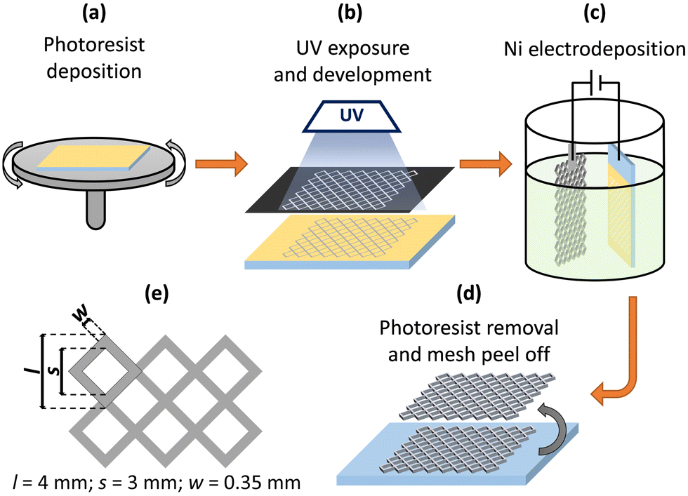 | ||
| Fig. 1 Sketch of the Ni mesh fabrication process. | ||
Watts electrolyte49 was used for the nickel electrodeposition (pH 4, (50 ± 2) °C, stirring); the composition in g L−1 of the electrolyte, after dilution in distilled water, was: NiSO4·6H2O (300), NiCl2·6H2O (35), and H3BO3 (45). The FTO-coated glass/photoresist and the platinum counter-electrode mesh were inserted in the electrolyte solution, parallel and at a distance from each other of 5 cm. An electrochemical station (Autolab PGSTAT302N) was then used to drive a constant cathodic current of 36.5 mA cm−2 for 10 min. The thickness of the deposited Ni layer estimated by SEM analysis (Fig. S1, ESI†) was (7.0 ± 0.1) μm.
2.2 Preparation of DSSCs
FTO-coated glass (2.2 mm, TEC7, GreatCell Solar) and bare soda-lime glass (3 mm, SGG PLANICLEAR, Saint-Gobain) were used as photoanode substrates and covers, respectively. A laser (355 nm nanosecond pulsed) was used to remove a section of the FTO layer (scribing) in the photoanode substrates and to drill the electrolyte injection holes in the cover glass. The substrates were ultrasonically washed with detergent and distilled water. After drying, the substrates were treated for 10 min in air plasma (Diener Electronics). A compact layer of TiO2 was deposited on the photoanode substrates by spray pyrolysis at 450 °C, using a precursor solution of titanium diisopropoxide bis(acetylacetonate) in anhydrous 2-propanol, followed by a 45 min sintering step. Afterwards, a ca. 7 μm transparent mesoporous TiO2 layer (Greatcell Solar 30 NR-D) was deposited and sintered at 500 °C for 1 h. DSSC devices of two sizes were prepared using square-shaped photoanodes: the smaller with a TiO2 area of 0.25 cm2 (denoted as S) and the larger with a TiO2 area of 6.25 cm2 (denoted as L). The substrates with the TiO2 layer were treated with a 40 mM TiCl4 aqueous solution at 70 °C for 30 min and sintered at 500 °C for 1 h. Afterward, a ca. 7 μm reflector/spacer TiO2 layer (WER2-O, Greatcell Solar) and a carbon layer (Elcocarb B/SP, Solaronix) were sequentially deposited and sintered at 500 °C and 400 °C, respectively for 1 h. The thickness of the carbon layer was varied by depositing several carbon paste layers; SEM was used to determine the carbon layer thickness (Fig. S2, ESI†).The substrates with the monolithic arrangement of DSSCs were immersed in a solution of 0.1 mM of the Y123 dye (Dyenamo) in tert-butanol/acetonitrile (1:1) %(v/v) for 48 h for the sensitization. Afterwards, the substrates were covered with bare glass and sealed with a 60 μm thick thermoplastic sealant (Meltonix 1170-60, Solaronix) in a hotpress at 160 °C. The devices were filled with cobalt electrolyte containing 0.165 M of Co(bpy)3(B(CN)4)2 (Eversolar Co-200), 0.045 M of Co(bpy)3(B(CN)4)3 (Eversolar Co-300), 1.2 M tert-butyl pyridine (TBP) and 0.1 M LiClO4 (Sigma Aldrich) in acetonitrile. The injection holes were sealed with Surlyn® and a circular-shaped microscope glass slide.
2.3 Preparation of perovskite solar cells
The PSCs were prepared on FTO-glass substrates (2.2 mm, TEC7, GreatCell Solar). The substrates were scribed and washed, as described in Section 2.2. Then, a TiO2 compact layer was deposited using the same method as for DSSCs. Afterward, mesoporous layers of TiO2 (T165/SP, Solaronix), ZrO2 (ZT-SP, Solaronix), and carbon (Elcocarb B/SP, Solaronix) were deposited by screen printing. After deposition, TiO2 and ZrO2 layers were sintered at 500 °C for 1 h and the carbon layer at 400 °C for 1 h. The perovskite precursor consisting of (5-AVA)0.05(MA)0.95PbI3 in γ-butyrolactone (GBL) solution (Solaronix) was dropped on top of the mesoporous layers and crystalized at 70 °C for 30 min in a hot plate.2.4 Application of the Ni mesh in/on the carbon counter-electrode
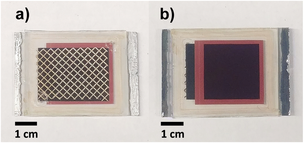 | ||
| Fig. 2 Photograph of a large-area DSSC with applied Ni-mesh on the carbon-counter electrode; view from the side of the cover glass (a) and FTO-glass (b). | ||
2.5 Characterization
The photocurrent–potential (J–V) curves were obtained under simulated solar light AM 1.5G, 100 mW cm2 from an Oriel class ABA LED solar simulator (MiniSol LSH 732; Newport). An electrochemical workstation (Zahner; Zennium) was employed to record the current vs. potential curves at 50 mV s−1 and 10 mV s−1 for DSSCs and PSCs, respectively. The PV devices were measured with a mask of 0.16 cm2 (small devices) and 5.29 cm2 (large devices). A batch of 4 devices was used for each test condition. The average values and the standard deviation for each batch are indicated in the tables. Characteristic J–V curves are presented for the device with the closest performance to the average value in a batch. Scanning electron microscopy (SEM) was characterized using a desktop SEM Phenom XL. The sheet resistance was measured using the Van der Pauw method with a Keithley 2425-C SourceMeter. The electrochemical impedance spectra (EIS) were collected in the dark in the frequency range of 1 MHz–0.1 Hz applying a sinusoidal perturbation with an amplitude of 10 mV at −0.85 V (DSSCs) and −0.80 V (PSCs). The EIS spectra were analyzed and fitted in ZView® software.3. Results and discussion
3.1 Characterization and effect of carbon counter-electrode thickness on the performance of the PV devices
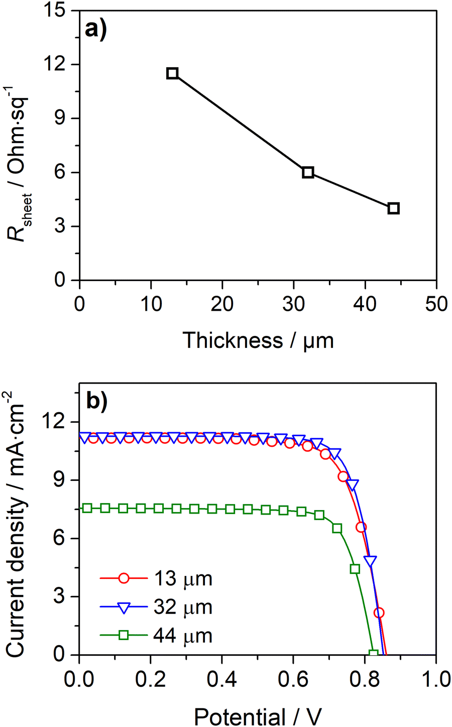 | ||
| Fig. 3 Measured Rsheetvs. thickness of screen-printed carbon layers (a), and J–V curves of small area (S) DSSCs with carbon counter electrodes of different thicknesses (b). | ||
A simple approach to improve the carbon-counter electrode conductivity is to increase its thickness (Fig. 3a). However, this approach has limited applicability since thick counter-electrodes can hinder the performance of devices, even in small-area devices, as indicated by the photovoltaic response (Fig. 3b) and metrics (Table S2, ESI†) of DSSCs with different carbon layer thicknesses.
The devices with 13 μm and 32 μm carbon films show similar photovoltaic responses with a power conversion efficiency (PCE) of ca. 7.3%. The cells generate an open-circuit potential (Voc) of ca. 0.87 V, a short circuit current density (Jsc) of ca. 11.2 mA cm−2, and a fill factor (ηFF) of ca. 0.77. The devices with a thicker 44 μm carbon layer displayed a much lower PCE of 4.5% due to a noticeably low Jsc of 7.0 mA cm−2. The low performance of devices with a thick carbon layer was assigned to the deficient sensitization of the mesoporous TiO2 layer; the photoanodes are unevenly stained and have areas with poor dye loading – Fig. S5 (ESI†). The thick carbon layer hinders the dye infiltration to the TiO2 layer, leading to deficient sensitization and underperforming devices.
3.2 Large-area PV devices with embedded Ni mesh
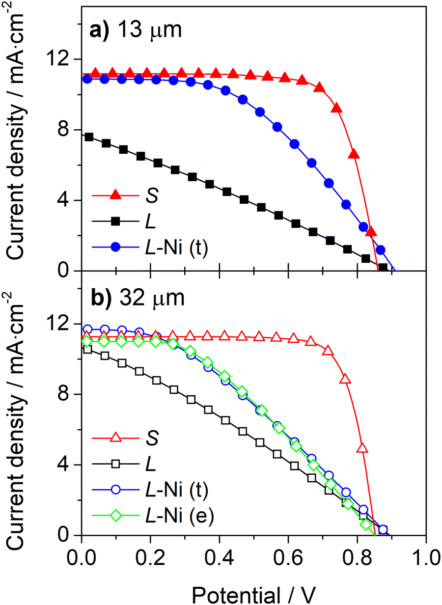 | ||
| Fig. 4 J–V curves of large-area DSSCs (L) with 13 μm (a) and 32 μm (b) carbon layers without and with Ni-mesh applied on top (t) or embedded (e) in the carbon layer; curves (S) represent the photovoltaic response of devices with a small area photoanode. | ||
| Carbon thickness/μm | Device | V oc/V | J SC/mA cm−2 | η FF | PCE/% |
|---|---|---|---|---|---|
| 13 | S | 0.86 ± 0.01 | 11.1 ± 0.1 | 0.75 ± 0.01 | 7.2 ± 0.1 |
| L | 0.89 ± 0.00 | 7.5 ± 0.2 | 0.28 ± 0.00 | 1.9 ± 0.1 | |
| L-Ni(t) | 0.90 ± 0.01 | 10.7 ± 0.6 | 0.46 ± 0.05 | 4.4 ± 0.2 | |
| 32 | S | 0.88 ± 0.00 | 11.3 ± 0.2 | 0.78 ± 0.00 | 7.4 ± 0.1 |
| L | 0.90 ± 0.01 | 10.8 ± 0.2 | 0.30 ± 0.01 | 2.9 ± 0.1 | |
| L-Ni(t) | 0.90 ± 0.01 | 11.3 ± 0.5 | 0.36 ± 0.01 | 3.7 ± 0.2 | |
| L-Ni(e) | 0.87 ± 0.02 | 10.4 ± 0.6 | 0.41 ± 0.01 | 3.8 ± 0.0 | |
Implementing the Ni-mesh on the counter-electrodes improves the performance of the devices, enhancing the photocurrent and the fill factor (Fig. 4 and Table 1). When Ni-mesh is applied on top of the 13 μm thick carbon layer, the ηFF and Jsc rise from 0.28 and 7.5 mA cm−2 to 0.46 and 10.7 mA cm−2, respectively; the PCE increased from 1.9% to 4.4%, translating to an impressive 132% improvement.
In the devices with a 32 μm carbon layer, the Ni-mesh was applied on top (t) or embedded (e) in the carbon layer. In both cases, the metallic mesh improved the photovoltaic response. The PCE of the cells was increased from 2.9% to 3.7% (t) and 3.8% (e). Applying the metallic mesh on the top of the carbon layer (L-Ni(t)) increased the fill factor by 20%; the Jsc had a minor improvement of 5%, and the Voc did not vary. When the mesh was embedded in the carbon layer (L-Ni(e)), the fill factor increased by 37%, while the Jsc and Voc decreased slightly by 3.7% and 3.3%, respectively. Overall, Ni-mesh, either on top or embedded in the carbon layer, improved the performance of DSSCs by ca. 29%.
The internal resistances were obtained by EIS analysis for the devices with and without the Ni-mesh on the counter-electrode. The Nyquist plots of the L, L-Ni, and S devices are shown in Fig. 5. The series resistance (Rs), charge transfer resistance at the counter electrode (RCE), and the electron recombination resistance at the photoanode (Rk) were obtained by fitting the spectra to the equivalent circuit model (Fig. 5c) to the EIS data and are presented in Table 2. QCPE_CE and QCPE_k are constant phase elements associated with the counter-electrode/electrolyte and photoanode/electrolyte interfaces, respectively.
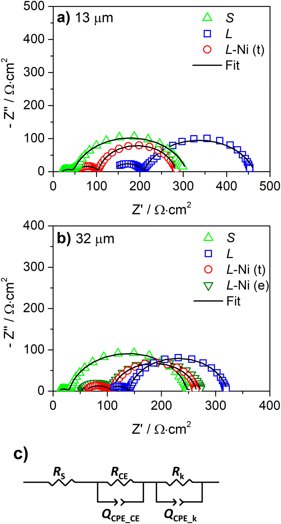 | ||
| Fig. 5 Nyquist diagrams of DSSCs with 13 μm (a) and 32 μm (b) carbon layer back contacts, for (S) small area devices, (L) large area devices without Ni-mesh applied, (L-Ni(t)) large area devices with Ni-mesh applied on top, and (L-Ni(e)) large area devices with Ni-mesh embedded in the counter-electrode layer; (c) equivalent circuit model used to fit the spectra. | ||
| Carbon thickness/μm | Device | R S/Ω cm2 | R CE/Ω cm2 | R k/Ω cm2 |
|---|---|---|---|---|
| 13 | S | 17.0 | 22.2 | 245.6 |
| L | 120.6 | 98.8 | 251.2 | |
| L-Ni(t) | 54.7 | 38.9 | 172.3 | |
| 32 | S | 8.4 | 17.4 | 201.2 |
| L | 100.5 | 39.8 | 180.6 | |
| L-Ni(t) | 53.9 | 37.9 | 137.3 | |
| L-Ni(e) | 52.1 | 37.2 | 119.4 | |
The small area devices show a lower Rs value when the carbon counter-electrode is thicker; this correlates with the sheet resistance of the carbon layers previously presented (Fig. 3a and Table S1, ESI†). Rs decreased from 17.0 to 8.4 Ω cm2 (Table 2) when the carbon counter-electrode thickness increased from 13 μm to 32 μm, and the sheet resistance of the carbon layers decreased from 11.5 to 6.0 Ω sq−1 for 13 μm and 32 μm layers, respectively (Table S1, ESI†).
Large-area devices without Ni-mesh show high Rs values, above 100 Ω cm2 (Table 2); the photovoltaic performance of L-cells is then greatly affected by the ohmic losses of the carbon-counter electrode. The poor conductivity of the carbon layer reduces the charge collection at the counter-electrode and limits the charge transfer process at the counter-electrode/electrolyte interface. L-cells with 13 μm and 32 μm carbon layers display an RCE of 100 Ω cm2 and 40 Ω cm2, respectively, considerably higher than for the small devices (S) with an RCE of only 20 Ω cm2. The higher RCE and Rs of the L devices with a 13 μm counter-electrode determined the inferior device performance compared with cells with a 32 μm carbon layer (Table 1). A minor difference in photovoltaic response was observed in small-area DSSCs with 13 μm and 32 μm carbon layers. These results confirm that the conductivity of the carbon layer is only relevant for the large-area cells.
The application of the Ni-mesh reduced the Rs of the L devices from above 100 Ω cm2 to ca. 53 Ω cm2. However, the Rs values are still higher compared to those of the small cells (<17 Ω cm2). The reason for that is the resistance of the FTO-coated glass when the device is scaled up.28 The prepared large-area cells with an embedded Ni-mesh at the counter-electrode display similar RCE values 37–39 Ω cm2. This shows that when used together with the metallic mesh, the thickness of the carbon layer has no effect on the charge transfer process at the counter electrode/electrolyte interface.
The conductivity of the counter-electrode is one of the decisive factors for obtaining high photocurrents and fill factors; it becomes especially critical for high irradiances (Fig. 6 and 7). Fig. 6 and Table S3 (ESI†) show the J–V curves and photovoltaic parameters of a DSSC device incorporating a 13 μm carbon layer counter-electrode with an embedded Ni-mesh for light irradiances ranging from 0.1 up to 2 suns; for this device, the current density continuously increases with the light irradiance. On the other hand, the photocurrent of a cell incorporating a simple 13 μm carbon layer counter-electrode (Fig. 6a) is similar for light irradiances above 1 sun since the conductivity of the counter-electrode limits the photogenerated current. Applying the Ni-mesh considerably increases the photocurrent at light irradiances above 1 sun (Fig. 6b). Moreover, the devices with Ni-mesh show higher ηFF for all light irradiances due to the improved conductivity of the counter-electrode.
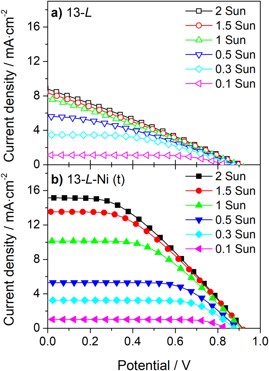 | ||
| Fig. 6 Incident light-dependent current-density vs. potential curves of large-area DSSCs with 13 μm carbon film (13-L) without (a) and with (b) Ni-mesh applied on top (t) of the carbon layer. | ||
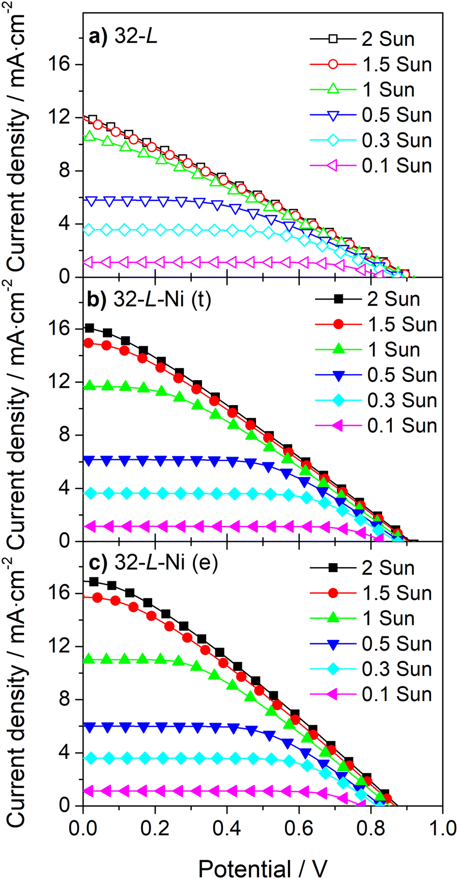 | ||
| Fig. 7 J–V curves at different incident light intensities for large-area DSSCs with 32 μm carbon film without (a) and with Ni-mesh applied on top (b) or embedded in the carbon layer (c). | ||
Similar to the devices incorporating a 13 μm carbon layer, embedding a Ni-mesh in a 32 μm carbon layer improves the ηFF of the devices at all light intensities (Fig. 7 and Table S4, ESI†), and its effect on the photocurrent of devices increases with the light intensity (Fig. 7b and c).
Even the current density of the large DSSC device, incorporating a counter-electrode thickness of 32 μm, is hindered by the ohmic losses at the carbon layer for light irradiances above 1 sun (Fig. 7a). This fact highlights that strategies for improving carbon-counter electrode conductivity are relevant and necessary for developing high-power output commercial devices.
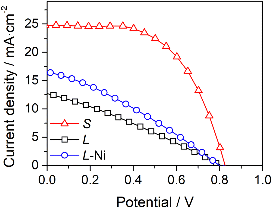 | ||
| Fig. 8 J–V curves of large-area PSCs (L) without and with Ni mesh along the small area device (S). | ||
| Device | V oc/V | J sc/mA cm−2 | η FF/% | PCE/% |
|---|---|---|---|---|
| S | 0.82 ± 0.01 | 24.8 ± 0.3 | 0.58 ± 0.01 | 11.9 ± 0.5 |
| L | 0.83 ± 0.01 | 12.9 ± 1.1 | 0.27 ± 0.00 | 2.9 ± 0.3 |
| L-Ni | 0.81 ± 0.01 | 16.3 ± 0.5 | 0.31 ± 0.02 | 4.1 ± 0.4 |
The application of a Ni-mesh reduced the Rs of large-area devices from 73.5 Ω cm2 to 36.5 Ω cm2. Small area devices (S) show Rs values of 18.9 Ω cm2, inferior to the L cells and similar to the DSSCs with the same carbon layer thickness. The higher Rs of large area PSCs with embedded Ni-mesh, compared to the small cells, implies that the photovoltaic performance of the devices is limited by the ohmic losses at the carbon layer but also at the TCO layer. Several strategies to improve the TCO layer conductivity are proposed in the literature39,40 and can be implemented and assessed in further research in combination with the Ni-mesh in the back-contact.
4. Conclusions
The poor conductivity of carbon-counter electrodes is a major obstacle to obtaining efficient scaled-up M-DSSCs and PSCs. Improving the conductivity of carbon electrodes by just increasing the carbon layer thickness has relevant drawbacks, namely related to the sensitization of the photoanode with the dye, in the case of the DSSC devices, and the perovskite absorber infiltration and crystallization, in the case of PSCs.This work addresses the low electric conduction of the carbon-based counter-electrodes by incorporating decal Ni-mesh on the carbon layer. The decal Ni-mesh was prepared by Ni electroplating on FTO-coated glasses; and photolithography was used to create the desired mesh pattern. The performance of the large-area M-DSSCs with 13 μm and 32 μm carbon layers and embedded Ni-mesh improved from 1.9% and 2.9% to 4.4% and 3.8%, respectively, mainly due to an improved ηFF and Jsc, showing that the best-performing counter-electrode was made of a 13 μm carbon layer with an embedded Ni-mesh. Moreover, for high incident light irradiances above 1 sun, the DSSC devices with a simple carbon layer as a counter-electrode showed a saturated current density. However, when a Ni-mesh was incorporated, the current density considerably increased with the irradiance above 1 sun.
An equivalent behavior was observed for the PSCs. When the Ni-mesh was applied to a large-area PSC, the power conversion efficiency increased from 2.9% to 4.1%. The improved performance when incorporating the Ni-mesh was assigned to a reduction to half of the series resistance, which decreased the ohmic losses of the carbon-based counter-electrode.
Electroplating Ni is a simple, low cost and widely used industrial process for various applications. The fabrication of the Ni-mesh by this method and the integration of a composite carbon–Ni counter-electrode into DSSC and PSC devices is advantageous for the upscaling of these technologies. A stand-alone Ni-mesh can easily be produced in different shapes and sizes and incorporated into other materials to improve their conductivity.
Conflicts of interest
The authors declare that they have no known competing financial interests or personal relationships that could have appeared to influence the work reported in this paper.Acknowledgements
Jorge Martins and Marta Pereira are grateful to the Portuguese Foundation for Science and Technology (FCT) for their PhD grant (references SFRH/BD/147201/2019 and 2021.06451.BD, respectively). This work was financially supported by: (i) LA/P/0045/2020 (ALiCE), UIDB/00511/2020, and UIDP/00511/2020 (LEPABE), funded by national funds through FCT/MCTES (PIDDAC); (ii) project 2SMART (NORTE-01-0145-FEDER-000054), supported by Norte Portugal Regional Operational Programme (NORTE 2020), under the PORTUGAL 2020 Partnership Agreement, through the European Regional Development Fund (ERDF); (iii) project TanPT (2022.05826.PTDC), funded by FEDER funds through COMPETE2020 – Programa Operacional Competitividade e Internacionalização (POCI) and by national funds (PIDDAC) through FCT/MCTES; (iv) project Diamond funded by the European Union's Horizon Europe Framework Programme for research and innovation Programme under the grant agreement no. 101084124; (v) alliance for energy transition (ATE) no. C644914747-00000023, project 56 of the Incentive System “Agendas for Business Innovation”, financed by the Recovery and Resilience Plan (PRR) and by European Funds NextGeneration EU.References
- M. Kokkonen, P. Talebi, J. Zhou, S. Asgari, S. A. Soomro, F. Elsehrawy, J. Halme, S. Ahmad, A. Hagfeldt and S. G. Hashmi, J. Mater. Chem. A, 2021, 9, 10527–10545 RSC.
- M.-J. Wu, C.-C. Kuo, L.-S. Jhuang, P.-H. Chen, Y.-F. Lai and F.-C. Chen, Adv. Energy Mater., 2019, 9, 1901863 CrossRef CAS.
- X. Xie, Y. Zhang, Y. Ren, L. He, Y. Yuan, J. Zhang and P. Wang, J. Phys. Chem. C, 2022, 126, 11007–11015 CrossRef CAS.
- C. Hora, F. Santos, M. G. F. Sales, D. Ivanou and A. M. Mendes, ACS Appl. Energy Mater., 2022, 5, 14846–14857 CrossRef CAS.
- L. Yuan, H. Michaels, R. Roy, M. Johansson, V. Öberg, A. Andruszkiewicz, X. Zhang, M. Freitag and E. M. J. Johansson, ACS Appl. Energy Mater., 2020, 3, 3157–3161 CrossRef CAS.
- G. Gianola, R. Speranza, F. Bella and A. Lamberti, Sol. Energy, 2023, 265, 112116 CrossRef CAS.
- S. Venkatesan, T.-H. Hsu, H. Teng and Y.-L. Lee, Solar RRL, 2023, 7, 2300220 Search PubMed.
- C. Teixeira, P. Spinelli, L. A. Castriotta, D. Müller, S. Öz, L. Andrade, A. Mendes, A. D. Carlo, U. Würfel, K. Wojciechowski and D. Forgács, Adv. Funct. Mater., 2022, 32, 2206761 CrossRef CAS.
- S. Mishra, S. Ghosh, B. Boro, D. Kumar, S. Porwal, M. Paul, H. Dixit and T. Singh, Energy Adv., 2022, 1, 761–792 RSC.
- G. Spinelli, M. Freitag and I. Benesperi, Sustainable Energy Fuels, 2023, 7, 916–927 RSC.
- A. Alberti, E. Smecca, S. Valastro, I. Deretzis, G. Mannino, C. Bongiorno, G. Fisicaro and A. La Magna, Phys. Chem. Chem. Phys., 2022, 24, 21549–21566 RSC.
- A. B. Muñoz-García, I. Benesperi, G. Boschloo, J. J. Concepcion, J. H. Delcamp, E. A. Gibson, G. J. Meyer, M. Pavone, H. Pettersson, A. Hagfeldt and M. Freitag, Chem. Soc. Rev., 2021, 50, 12450–12550 RSC.
- L. Wang, G.-R. Li, Q. Zhao and X.-P. Gao, Energy Storage Mater., 2017, 7, 40–47 CrossRef.
- L. Liang, Y. Cai, X. Li, M. K. Nazeeruddin and P. Gao, Nano Energy, 2018, 52, 211–238 CrossRef CAS.
- M. Que, B. Zhang, J. Chen, X. Yin and S. Yun, Mater. Adv., 2021, 2, 5560–5579 RSC.
- K. Domanski, J. P. Correa-Baena, N. Mine, M. K. Nazeeruddin, A. Abate, M. Saliba, W. Tress, A. Hagfeldt and M. Gratzel, ACS Nano, 2016, 10, 6306–6314 CrossRef CAS PubMed.
- N. N. Shlenskaya, N. A. Belich, M. Grätzel, E. A. Goodilin and A. B. Tarasov, J. Mater. Chem. A, 2018, 6, 1780–1786 RSC.
- L. Fagiolari and F. Bella, Energy Environ. Sci., 2019, 12, 3437–3472 RSC.
- A. Kay and M. Grätzel, Sol. Energy Mater. Sol. Cells, 1996, 44, 99–117 CrossRef CAS.
- D. Bogachuk, R. Tsuji, D. Martineau, S. Narbey, J. P. Herterich, L. Wagner, K. Suginuma, S. Ito and A. Hinsch, Carbon, 2021, 178, 10–18 CrossRef CAS.
- M. A. K. L. Dissanayake, J. M. K. W. Kumari, G. K. R. Senadeera, T. Jaseetharan, J. Weerasinghe and H. Anwar, Mater. Sci. Eng., B, 2021, 273, 115440 CrossRef CAS.
- L. Zhang, T. Liu, L. Liu, M. Hu, Y. Yang, A. Mei and H. Han, J. Mater. Chem. A, 2015, 3, 9165–9170 RSC.
- A. S. A. Ahmed, W. Xiang, F. S. M. Hashem and X. Zhao, Sol. Energy, 2021, 230, 902–911 CrossRef CAS.
- R. Cruz, J. P. Araújo, L. Andrade and A. Mendes, J. Mater. Chem. A, 2014, 2, 2028–2032 RSC.
- P. Mariani, A. Agresti, L. Vesce, S. Pescetelli, A. L. Palma, F. Tomarchio, P. Karagiannidis, A. C. Ferrari and A. Di Carlo, ACS Appl. Energy Mater., 2021, 4, 98–110 CrossRef CAS.
- C. O. Teixeira, L. Andrade and A. Mendes, Int. J. Energy Res., 2019, 43, 7541–7546 CAS.
- Y. Wang, H. Zhao, Y. Mei, H. Liu, S. Wang and X. Li, ACS Appl. Mater. Interfaces, 2019, 11, 916–923 CrossRef CAS.
- F. Yu, Y. Shi, W. Yao, S. Han and J. Ma, J. Power Sources, 2019, 412, 366–373 CrossRef CAS.
- F. Meng, Y. Zhou, L. Gao, Y. Li, A. Liu, Y. Li, C. Zhang, M. Fan, G. Wei and T. Ma, Mater. Today Energy, 2021, 19, 100590 CrossRef CAS.
- M. Bidikoudi, V. Dracopoulos and E. Stathatos, Energy Adv., 2022, 1, 76–86 RSC.
- N. Ahn, I. Jeon, J. Yoon, E. I. Kauppinen, Y. Matsuo, S. Maruyama and M. Choi, J. Mater. Chem. A, 2018, 6, 1382–1389 RSC.
- M. Wu, M. Sun, H. Zhou, J.-Y. Ma and T. Ma, Adv. Funct. Mater., 2020, 30, 1906451 CrossRef CAS.
- D. Raptis, V. Stoichkov, S. M. P. Meroni, A. Pockett, C. A. Worsley, M. Carnie, D. A. Worsley and T. Watson, Curr. Appl. Phys., 2020, 20, 619–627 CrossRef.
- P. Meredith and A. Armin, Nat. Commun., 2018, 9, 5261 CrossRef CAS PubMed.
- L. Gao, L. Chen, S. Huang, X. Li and G. Yang, ACS Appl. Energy Mater., 2019, 2, 3851–3859 CrossRef CAS.
- A. I. Pereira, J. Martins, C. J. Tavares, L. Andrade and A. Mendes, Appl. Surf. Sci., 2017, 423, 549–556 CrossRef CAS.
- B. Wilkinson, N. L. Chang, M. A. Green and A. W. Y. Ho-Baillie, Prog. Photovoltaics Res. Appl., 2018, 26, 659–674 CrossRef.
- K. Okada, H. Matsui, T. Kawashima, T. Ezure and N. Tanabe, J. Photochem. Photobiol., A, 2004, 164, 193–198 CrossRef CAS.
- D. Ivanou, J. Capitão, J. Maçaira, A. I. Pereira and A. Mendes, J. Electrochem. Soc., 2018, 165, H1040–H1046 CrossRef CAS.
- V. C. M. Duarte, D. Ivanou, G. Bernardo, L. Andrade and A. Mendes, Int. J. Energy Res., 2022, 46, 5288–5295 CrossRef.
- A. Khan, C. Liang, Y.-T. Huang, C. Zhang, J. Cai, S.-P. Feng and W.-D. Li, Adv. Eng. Mater., 2019, 21, 1900723 CrossRef CAS.
- A. Khan, Y.-T. Huang, T. Miyasaka, M. Ikegami, S.-P. Feng and W.-D. Li, ACS Appl. Mater. Interfaces, 2017, 9, 8083–8091 CrossRef CAS.
- K. Miettunen, T. Saukkonen, X. Li, C. Law, Y. K. Sheng, J. Halme, A. Tiihonen, P. R. F. Barnes, T. Ghaddar, I. Asghar, P. Lund and B. C. O’Regan, J. Electrochem. Soc., 2012, 160, H132–H137 CrossRef.
- Z. Ku, X. Xia, H. Shen, N. H. Tiep and H. J. Fan, Nanoscale, 2015, 7, 13363–13368 RSC.
- H. P. Feng, T. Paudel, B. Yu, S. Chen, Z. F. Ren and G. Chen, Adv. Mater., 2011, 23, 2454–2459 CrossRef CAS PubMed.
- G.-R. Li and X.-P. Gao, Adv. Mater., 2020, 32, 1806478 CrossRef CAS PubMed.
- M. Mohammadnezhad, G. S. Selopal, N. Alsayyari, R. Akilimali, F. Navarro-Pardo, Z. M. Wang, B. Stansfield, H. Zhao and F. Rosei, J. Electrochem. Soc., 2018, 166, H3065–H3073 CrossRef.
- H. G. Lemos, D. Barba, G. S. Selopal, C. Wang, Z. M. Wang, A. Duong, F. Rosei, S. F. Santos and E. C. Venancio, Sol. Energy, 2020, 207, 1202–1213 CrossRef CAS.
- G. A. Di Bari, Modern Electroplating, 2010, pp. 79–114. DOI:10.1002/9780470602638.ch3.
- S. Sarker, H. W. Seo, Y.-K. Jin, M. A. Aziz and D. M. Kim, Mater. Sci. Semicond. Process., 2019, 93, 28–35 CrossRef CAS.
- R. B. H. Tahar, T. Ban, Y. Ohya and Y. Takahashi, J. Appl. Phys., 1998, 83, 2631–2645 CrossRef.
- S. Ngamsinlapasathian, T. Sreethawong, Y. Suzuki and S. Yoshikawa, Sol. Energy Mater. Sol. Cells, 2006, 90, 2129–2140 CrossRef CAS.
- S. Sheehan, P. K. Surolia, O. Byrne, S. Garner, P. Cimo, X. Li, D. P. Dowling and K. R. Thampi, Sol. Energy Mater. Sol. Cells, 2015, 132, 237–244 CrossRef CAS.
- Q. Wei, Z. Yang, D. Yang, W. Zi, X. Ren, Y. Liu, X. Liu, J. Feng and S. Liu, Sol. Energy, 2016, 135, 654–661 CrossRef CAS.
- A. Mei, X. Li, L. Liu, Z. Ku, T. Liu, Y. Rong, M. Xu, M. Hu, J. Chen, Y. Yang, M. Grätzel and H. Han, Science, 2014, 345, 295 CrossRef CAS PubMed.
- D. Li, P. Jiang, W. Zhang, J. Du, C. Qiu, J. Liu, Y. Hu, Y. Rong, A. Mei and H. Han, Solar RRL, 2021, 2100554 Search PubMed.
- A. Verma, D. Martineau, S. Abdolhosseinzadeh, J. Heier and F. Nüesch, Mater. Adv., 2020, 1, 153–160 RSC.
- A. Priyadarshi, L. J. Haur, P. Murray, D. Fu, S. Kulkarni, G. Xing, T. C. Sum, N. Mathews and S. G. Mhaisalkar, Energy Environ. Sci., 2016, 9, 3687–3692 RSC.
- J. Du, C. Qiu, S. Li, W. Zhang, W. Zhang, Y. Wang, Z. Qiu, Q. Wang, K. Yang, A. Mei, Y. Rong, Y. Hu and H. Han, Adv. Energy Mater., 2022, 12, 2102229 CrossRef CAS.
- Y. Xia, X. Chen, Z. Zheng, X. Xiao, C. Ling, M. Xia, J. Gong, L. Gao, J. Xiang, Y. Hu, A. Mei, Y. Rong and H. Han, J. Phys. Chem. Lett., 2022, 13, 2144–2149 CrossRef CAS PubMed.
- K. Chen, Z. L. Zhang, J. Liu, Y. Huang, D. J. Wang, B. She, B. C. Liu, X. L. Zhang and J. Zhang, Adv. Mater. Interfaces, 2022, 9, 2100395 CrossRef CAS.
- C. Xu, Z. Zhang, Y. Hu, Y. Sheng, P. Jiang, H. Han and J. Zhang, J. Energy Chem., 2018, 27, 764–768 CrossRef.
- S. G. Hashmi, D. Martineau, X. Li, M. Ozkan, A. Tiihonen, M. I. Dar, T. Sarikka, S. M. Zakeeruddin, J. Paltakari, P. D. Lund and M. Grätzel, Adv. Mater. Technol., 2017, 2, 1600183 CrossRef.
Footnote |
| † Electronic supplementary information (ESI) available. See DOI: https://doi.org/10.1039/d3ya00476g |
| This journal is © The Royal Society of Chemistry 2024 |