
 Open Access Article
 This Open Access Article is licensed under a
 Creative Commons Attribution 3.0 Unported Licence
Nanoscale spatial and time-resolved mapping in perovskite and organic solar cells: a multimodal technique to visualize the photoinduced charge dynamics
M. Bilal
Faheem†
 ,
Yuchen
Zhang†
,
Madan Bahadur
Saud
,
Hansheng
Li
,
Poojan Indrajeet
Kaswekar
and
Quinn
Qiao
*
,
Yuchen
Zhang†
,
Madan Bahadur
Saud
,
Hansheng
Li
,
Poojan Indrajeet
Kaswekar
and
Quinn
Qiao
*
Energy Conversion and Storage Lab, Department of Mechanical and Aerospace Engineering, Syracuse University, Syracuse 13244, USA. E-mail: quqiao@syr.edu
First published on 16th May 2024
Abstract
Recently, perovskite solar cells (PSCs) and organic solar cells (OSCs) have emerged as solution-processable photovoltaic (PV) technologies with certified power conversion efficiencies (PCEs) surpassing 26% and 20%, respectively. However, challenges such as charge generation, separation, transport, collection, and recombination at the nanoscale still exist in fully controlling and understanding the performance-limiting factors in the photoactive layers of OSC and PSC devices. Although several efforts have been reported to address the above phenomena, the origin of the nanoscale defects and how they lead to performance losses have not yet been fully understood. This perspective provides an in-depth discussion of nanoscale spatial and time-resolved mapping for OSCs and PSCs to understand their roles in improving PV performance. A comprehensive multimodal technique to map the charge carrier photodynamics at the nanoscale, such as charge generation, separation, transport, collection, and recombination in OSCs and PSCs, is presented, which has the potential to evaluate the photodynamics related to local heterogeneities in the active layers of the corresponding devices.
 M. Bilal Faheem | M. Bilal Faheem is Research Assistant of Prof. Quinn Qiao in the Energy Conversion and Storage Lab, at the Department of Mechanical and Aerospace Engineering, Syracuse University. His research interests include the synthesis of perovskite solar cells and nanoscale photodynamics mapping in organic and perovskite solar cells and LEDs through conventional and multi-modal AFM. |
 Yuchen Zhang | Yuchen Zhang is a 3rd year PhD student under the supervision of Prof. Quinn Qiao in the Energy Conversion and Storage Lab, at the Department of Mechanical and Aerospace Engineering, Syracuse University. His research interests include nanoscale photodynamics mapping in organic and perovskite solar cells and LEDs. |
 Madan Bahadur Saud | Madan Bahadur Saud is a 3rd year PhD student under the supervision of Prof. Quinn Qiao in the Energy Conversion and Storage Lab, at the Department of Mechanical and Aerospace Engineering, Syracuse University. His research interests include the synthesis and characterization of sulfide and polymer solid electrolytes, and their implementation into all-solid-state lithium metal batteries by using various interfacial engineering approaches, and the characterization of perovskite solar cells. |
 Hansheng Li | Hansheng Li is a 3rd year PhD student under the supervision of Prof. Quinn Qiao in the Energy Conversion and Storage Lab, at the Department of Mechanical and Aerospace Engineering, Syracuse University. His research interests include the synthesis of LMRO cathodes for high-capacity Lithium metal batteries and the characterization of perovskite Solar Cells. |
 Poojan Indrajeet Kaswekar | Poojan Indrajeet Kaswekar is a 3rd year PhD student under the supervision of Prof. Quinn Qiao in the Energy Conversion and Storage Lab, at the Department of Mechanical and Aerospace Engineering, Syracuse University. His research interests include the synthesis and characterization of narrow-bandgap Sn-based perovskite solar cells. |
 Quinn Qiao | Professor Quinn Qiao is currently a professor in the Department of Mechanical and Aerospace Engineering at Syracuse University. He serves as the site director of the NSF IUCRC Center for Solid-State Electric Power Storage (CEPS). As principal investigator and head of the Energy Conversion and Storage Lab, his expertise lies in innovative perovskite materials for photovoltaic energy conversion, with a particular focus on synthesizing and characterizing rechargeable lithium batteries. |
Introduction
Thin film solar cells fabricated through solution-processed deposition techniques have revolutionized the field by placing themselves near silicon (Si)-based photovoltaics. Recently, OSCs and PSCs have presented tremendous improvements in their PCE and operational stability, and it is believed that they will soon be commercialized and challenge the market occupancy of Si solar cells. The PCE of OSCs containing a conjugated polymer donor and a small organic molecule acceptor1 has recently exceeded 20%,2,3 which is mainly driven by the engineering of the device architecture, dynamics of the photoactive material, and improved thin film morphology. The PCE of PSCs, on the other hand, have surpassed 26%4,5 while placing themselves near the single-crystalline Si-based solar cells in terms of device efficiency, through the efforts made in compositional tuning, materials processing, and choice of charge carrier transport layers (CTLs).6–8 Both OSCs and PSCs are relatively new technologies compared to traditional Si-based solar cells, and present similar device architectures.9–12 The understanding of the fundamental processes underlying the function of OSCs and PSCs has also advanced; however, there are still certain aspects that are not fully understood and are actively being researched. These aspects include various mechanisms for generating, transporting, and recombining photogenerated charge carriers within the devices, at length scales ranging from crystalline grains to sub-grains and atomic levels. In both types of solar cells, photophysics (the study of the interaction between light and matter) and charge carrier dynamics play crucial roles in determining the overall PCE of the devices. To improve the overall PCE and hence the operational stability of these devices, it is essential to have a deep understanding of the photodynamics and charge carrier kinetics of active layer absorbers in OSCs and PSCs.9,12 Some key differences between the two systems are outlined below.In photoinduced charge carrier generation in OSCs, light absorption leads to the formation of excitons (bound electron–hole pairs) within the organic semiconductor and these excitons must be dissociated into free carriers (photoelectrons and photo-holes) at the donor–acceptor heterojunction to generate photocurrent. In contrast, PSCs directly generate free carriers upon photoexcitation of the perovskite absorbers. OSCs typically exhibit hopping-like carrier transport, where charges move through the organic semiconductor via localized states and this transportation type is associated with the disordered nature of organic materials. In PSCs, carrier transport occurs through band-like transport, like conventional inorganic semiconductors, due to the crystalline nature of perovskite semiconductors.13,14 The majority of OSCs utilize a bulk heterojunction structure, consisting of a blend of donor and acceptor materials, which allows for efficient exciton dissociation and charge separation at the interface between the donor and acceptor phases. PSCs, on the other hand, do not typically require a donor–acceptor heterojunction structure as the perovskite material itself acts as both the light absorber and charge transporter but they are known to contain relatively mobile ions, typically organic or inorganic cations, within the perovskite active layer absorber.14 These ions can contribute to device PCE and stabilize the power output by assisting with defect passivation and ionic migration, which is not the case with OSCs.10
Fig. 1a and b explains the operational mechanisms of OSC and PSC devices, respectively, which are based on light absorption and, in effect, the separated charge carriers through the photoactive layer.15 In both OSC and PSC devices, the ultrafast charge carrier dynamics, of the order of picoseconds, is critically important for understanding the behavior of charge carriers; however, the temporal sensitivity of their systems is limited to tens to hundreds of nanometers and they extract lifetimes of several microseconds,15,16 as represented in Fig. 1a.10 Upon photoexcitation, the low dielectric constant of organic semiconductors leads to the formation of Frenkel excitons; this separation process is driven by the energy offsets between the electronic energy levels of the donor and acceptor species. These excitons are localized electron–hole pairs and typically exhibit lifetimes ranging from approximately 20 picoseconds (ps) to 1 ns in neat organic semiconductor films. Exciton diffusion lengths, which represent how far the excitons can travel before dissociation, range from approximately 3 to 20 nm. Moreover, the separation of these excitons into free charges (electrons and holes) is primarily achieved at the interfaces between the organic donor and acceptor materials, which are often referred to as charge carrier transfer (CT) states. On the other hand, PSCs are comprised of mixed semiconductor absorber layers, which are usually synthesized through two or more precursors dissolved in some suitable polar aprotic solvents (dimethyl formamide (DMF), dimethyl sulfoxide (DMSO), n-methylpyrrolidone (NMP), etc.) and in the majority of cases, the spin coating of the precursor solution onto the substrate and post-annealing at optimal temperatures produce a uniform thin film of the perovskite active layer (PAL).17 Therefore, the operational mechanism of PSCs is comparatively less complex as represented in Fig. 1b.10 Upon photo-absorption, free electrons and holes are generated inside the PAL, which are transported through CTLs and collected at the respective electrodes to derive the electronics of the external circuit. The photogeneration within the PAL is attributed to the lower binding energies resulting from the higher dielectric constants and crystalline nature of perovskites. The ultrafast carrier dynamics in PSCs are less detrimental to the overall PCE, unlike OSCs. Various optical techniques are commonly employed to investigate the carrier dynamics and understand the performance and stability of these solar cell technologies (OSCs and PSCs). Photoluminescence (PL) spectroscopy provides information about the radiative recombination processes and the efficiency of charge carrier generation in active materials.18–20
 | ||
| Fig. 1 Operational mechanism of (a) OSCs and (b) PSCs.10 Reproduced from ref. 10 with permission from John Wiley and Sons, copyright 2021. (c) Schematic illustration of c-AFM on the surface of a MAPbI3−xClx PSC. (d) Topographical image of MAPbI3−xClx. (e) Comparison of heterogeneity for ISC and VOC with the corresponding facets; areas in blue (high VOC and ISC), and areas in red (low VOC and ISC) are overlaid on the local topography.38 Reproduced from ref. 38 with permission from Springer Nature, copyright 2016. (f) Schematic illustration of photoconductive tomographic-AFM with bottom illumination. (g) Volumetric perspective of the photocurrent distribution throughout the MAPbI3 thin film by T-AFM. (h) AFM topography image (6 μm × 6 μm) of the MAPbI3 surface before T-AFM. (i) Segmented cross-sectional tomograms of GBs and grains respectively, revealing Type-I GBs at and hidden beneath the surface along the blue long-dashed line from (h). Cross-sectional tomogram of Type-I and insipid Type-II GBs, along profiles respectively indicated by the magenta dotted line and yellow dashed line in (h). (j) Specific interfaces highlighted by overlain ovals, demonstrating absolute through-thickness differences in photocurrents for Type I and II GBs, despite being topographically indistinguishable at the surface.39 Reproduced from ref. 39 with permission from Springer Nature, copyright 2020. | ||
Transient absorption spectroscopy (TAS) allows the study of excited states and charge carrier dynamics by monitoring changes in the absorption of the material following photoexcitation.20–22 Some recently deployed techniques for evaluating multiple nanoscale properties simultaneously in OSC and PSC devices are termed multimodal techniques.23,24 Such techniques include transmission electron microscopy (TEM)25,26 and photoinduced force microscopy (PiFM),27–30etc., with their multiple testing modes to evaluate the structure–property–function and performance relationships among the common and complex parameters over nanoscales.31–33 Although various characteristics can be inferred from parallel techniques, multimodal measurements allow direct relationships with enhanced precision. Direct measurements through such techniques are important in perovskite and organic semiconductors because they are very sensitive to the processing conditions. In both kinds of devices, the local (nanoscale) structures and properties may vary from sample to sample and over different pixelates, making it challenging to have precision on the same region under scanning. Herein, we represent a brief review of the multimodal atomic force microscopy (AFM) technique that can precisely and quantitatively characterize semiconductor thin films against their critical photodynamics such as charge carrier diffusion length (LD), carrier recombination lifetime (τr), carrier transport time (τt), carrier density, etc. In the meantime, we refer the readers to other reports regarding crystal growth investigations and thin film formation through bulk multimodal strategies. Some device performances lag in PSCs and OSCs, including intrinsic disorders such as current–voltage (JV) hysteresis, ion migration, and trap-assisted recombination. Recently a multimodal characterization study of local nanoscale phase impurities,34 such as carrier traps and PCE degradation sites, was revealed by Stranks et al.33,35 A hexagonal polytype perovskite structure (with segregated iodine, even in a trace amount) as the minority phase caused by the photochemical degradation of the formamidinium (FA)-rich perovskite composition was investigated as a major responsible factor for deteriorating the carrier dynamics in PSCs.35–37 Because the PALs are polycrystalline, there are several grain boundaries (GBs) with very weak dangling bonds, which act as the recombination pathways limiting the overall PCE and operational stability of PSCs.40–42 In another study by Bao et al.,43 a multidimensional nano-spectroscopic imaging technique was presented to map the heterogeneities in local charge recombination within the indium phosphide nanowires at 40 nm hyperspectral resolution. However, this technique was never deployed to map the properties of perovskite or organic polymeric structures against their local carrier dynamics. There is still a large gap in the fundamental understanding of charge carrier behaviors in GBs and the surrounding locations in the grain crystallites, termed grain interiors, in this report. In PSC research, there has been a contradiction regarding the role of GBs as benign in carrier transport;40,44 however, many studies have reported their adverse effects on the carrier dynamics.40,45,46 Spatially resolved measurements are required to understand the qualitative view of the heterogeneities in GBs.33 Weaker PL intensities and shorter carrier lifetimes were observed for the GBs to spatially investigate the carrier dynamics, which further suggested that GBs act like carrier recombination centers.34,47 GBs are vertically aligned but still have detrimental effects on the photodynamics of PV devices. Some conventional microscopy techniques were also used for the spatial resolution of the carrier lifetimes, photocurrent testing, and trap-density maps to explain the dominant carrier-trapping and de-trapping processes in PSCs but these techniques were unable to correlate the microstructural evolutions and the carrier dynamics in GBs at the nanoscale.48 Conductive AFM (c-AFM) is reported to be a powerful technique, which has the potential to map the inhomogeneities in charge carrier concentrations and local photocurrent at the GBs and evaluate the facet-dependent photovoltaic performance mishmashes in thin film solar cells and PSCs.38,42,49 PSCs and OSCs with different active layer morphologies were reported with the mapping of local photocurrent hysteresis, photovoltage, photocurrent, and the variations in photovoltaic performance at the nanoscale, with the relationship between grain size and photocurrent.24 These reports lack experimental evidence for simultaneously mapping the nanoscale photodynamics such as carrier lifetime, transport time, and diffusion length in photoactive microstructures.
Nanoscale photodynamics mapping
Leblebici and co-workers reported, for the first time, the practical realization of local short-circuit photocurrent, open circuit photovoltage, and dark drift current in MAPbI3 solar cells using photoconductive (pc)-AFM.38 They observed significant variations in both ISC and VOC, indicating, by extension, fluctuations in local efficiency across the characterized area of about 4 μm2. This variability is pronounced to the extent that certain regions exhibit negligible electronic activity, resulting in minimal power output. Moreover, even within a single-crystalline grain, there is apparent performance heterogeneity. A preliminary examination of the data suggested that approximately 5% of the area showed no current generation, and most of the area produced currents below the peak values.38,42Fig. 1c represents the schematics of the modified AFM, showing that the tip approaches each pixelate to map the photocurrent, and retracts50 to move to the next pixel. Unlike traditional c-AFM, the modified instrument eliminated friction, leading to a decrease in tip-sample wear and material transfer while ensuring a consistent contact area during current measurements. The topography image in Fig. 1d represents the distinct crystal grains and diverse crystal facets within the grains. The variety of grain shapes observed in the topography image is attributed to the absence of any preferential grain orientation in the MAPbI3−xClx perovskite films. Fig. 1e explains the overlap of topography in grey scales with the blue pixelates representing the high-efficiency regions with VOC > 0.6 V and ISC > 12 pA and low-efficiency regions (red pixels) with VOC > 0.6 V and ISC < 5 pA. Their results demonstrated the observed spatial variation as an intrinsic characteristic of the corresponding PSC without the interactions between the tip and the sample material, indicating that many grains have a specific crystal facet that facilitates higher performance. Another devised and exclusive method utilizing tomographic AFM was reported by Huey et al. as they presented a comprehensive 3D map of photogenerated carrier transport at the nanoscale in hybrid perovskites. This unveils GBs functioning as extensively interconnected conducting pathways for carrier transport. The presence of buried GB types in hybrid perovskites was revealed (Schematics Fig. 1f), some of which were slightly inert while some GBs heightened carrier mobilities.39Fig. 1g represents the photocurrent tomogram obtained for polycrystalline MAPbI3, derived from 34 initial images, collectively encompassing a total of 7.6 million pixels (11.7 nm × 11.7 nm) of photocurrent and (x, y, z) position data. The assessment of the milling and interpolation distances indicated that over 95% of all tomogram voxels were situated close to just two adjacent nearest neighbors from the initially acquired data. Throughout this process, consistent measurements of photocurrents ranging from 100 pA to 10 nA were obtained, with dark current detection below 10 pA under the same DC bias. They performed a thorough analysis of 2D-mapping (for photocurrent and photovoltage) through photoconductive (pc)-AFM51 and 3D-mapping through tomographic (T)-AFM, over the type and influence of GBs on the photodynamics of the MAPbI3 perovskite thin film. A precise comparison of the topography was studied and represented in Fig. 1h with the corresponding photoconduction maps derived from our tomographic approach; both GB types can easily be differentiated. In Fig. 1i, cross-sectional tomograms show the segmentation of the 3D GB network and the 3D grain photoconductivity. Numerous type-I GBs are identifiable, including those concealed within the film and undetectable through traditional surface measurements. Notably, on the upper left side of Fig. 1i, the higher and lower photocurrents within neighboring grains explicitly demonstrate the anticipated type-I behavior, which hinders the in-plane inter-grain charge carrier diffusion. On the contrary, the more elusive type-II interfaces at the surfaces become evident in T-AFM results, as exemplified in Fig. 1j (corresponding to Fig. 1h).39 In each instance, two seemingly distinct grains are separated by a topographic GB groove that is morphologically indistinguishable from other GBs, while the photocurrents at the surface and beneath the surface remain uniform. Importantly, neither type-I nor type-II GBs show any correlation with low or high load AFM scan directions, as evidenced in specific instances oriented at −85° (blue oval, including numerous other type-I GBs), −20° (yellow oval, type-II), and −70° (magenta oval, type-II) with respect to the horizontally scanning probe (0°).39 Conclusively, an interconnected network of type-I GBs revealed a pathway for charge carriers in 3D and the presence of about 5% of benign type-II GBs52,53 restricted the out-of-plane conduction and exhibited in-plane carrier transport. Type-II or twin GBs53 have fewer detrimental effects (which may be attributed to their lower number density) on the photodynamics of perovskite semiconductors, while type-I GBs were proved to have adverse effects on the carrier dynamics.39 The techniques presented so far with customized AFM relied on the full illumination of the samples either from the top or bottom side and may face severe phase segregation; the reports lack this critical aspect while explaining the direct relationship of the facet or GB-dependent performance evaluations. In the earlier study presented by Leblebici et al.38 and represented here, the only conditioning to avoid phase segregation is a minimized time of contact between the AFM-tip and sample surface; however, continuous illumination (Fig. 1c–f) may leave the perovskite with severe halide segregation.54,55 Another effort was made by de Quilettes et al.34 as they analyzed the relationship between the local heterogeneity of the MAPbI3 perovskite and the photocurrent and device performance yields through the high-resolution (sub-micrometer) laser beam-induced current/voltage mapping and spatially resolved pc-AFM. An anti-correlation was found between the measurements taken from the PL and pc-AFM for the device with CTL and top contact and the device without, considering the same sample area under observation for both types of measurements (PL, pc-AFM). The regions with higher PL showed lower photocurrent and efficiency, highlighting the obvious disparity between the two measurements, and prospecting the crucial role of the top contact in mitigating the losses in the PSC devices. The investigated correlation is likely due to discrepancies in the perovskite absorber where variations in its surface lead to fluctuations in electronic coupling with the extraction layers. Consequently, although material heterogeneity may pose limitations to device performance in the long run, it was not the primary determinant in the performance evaluation of PSC devices. In all the previous reports regarding the multimodal AFM technique, the perovskite under observation was MAPbI3, which is not the highest-performing perovskite process for solar cells. Subsequent research proved that the MAPbI3-based PSCs suffered degradation losses and other compositional analogues such as the cations and anions mixing within perovskite absorbers yielded extraordinary outputs.56,57 Since the advent of such modified techniques, there are still very few studies regarding the underlying technique for the simultaneous and quantitative analyses of carrier recombination lifetime, transport time, and diffusion length; our group published a similar but comparatively more precise multimodal nanoscale mapping technique for spatial and time-resolved analyses of charge carrier photodynamics.58 To best explain the structure–property (microstructure-photodynamics) relationship of the photoactive layer, and to gain further insights into the behavior of photogenerated charge carriers, the contact mode c-AFM-enhanced nanoscale mapping technique has been proven to be better than other previously reported techniques. The formerly explained techniques were deployed to study the carrier dynamics under the full illumination of the sample from either the top or the bottom, and are critical for avoiding the halide segregation and ion migration through the GBs of the bulk perovskite. The c-AFM is used to probe local charge-carrier dynamics in photoactive layers with improved spatial resolution at the nanometer scale38 (the actual resolution of the measurement was about 9.26 nm)58 and overcome the obstacles of the normal AFM circuit bandwidth to detect the local characteristics including transient parameters (τr,τt and LD) and with improved temporal resolution by pulse widths from a function generator driving the optical source ranging from 50 ns to 500 ns. Fig. 2a shows a schematic diagram of the customized transient photo-response AFM (TP-AFM) instrumentation setup where the PSC or OSC can be mounted in a c-AFM configuration with an RGB laser illumination, a Breakout Box (Agilent N9447A) and a mixed signal oscilloscope (Agilent MSOX4154A) to measure transient photovoltage (TPV) and transient photocurrent (TPC) by using a platinum/chromium-coated conductive tip.59 With the tip movement across the surface, the TPV and TPC charge carrier dynamics mapping can be generated based on the transient decay data from the synchronization of the laser pulse, illuminating the underside of the sample under observation. The lower right part of Fig. 2a demonstrates the synchronization of the AFM-tip and the laser pulse for each movement at each pixel on the PAL. Fig. 2b represents the device equivalent circuit with an alternative sampling resistor. When Ro = 1 MΩ, the device was in open circuit conditions to record TPV, which was processed to obtain the measured τr of the solar cell. When Ro = 50 Ω, the device was in a short circuit and recording TPC, which was processed to obtain τt. For PSCs, a 100 × 100 nm2 region (sufficient to encompass both the adjacent perovskite grains and clear GB) was selected and the mapping region is derived from the c-AFM topography image.58 For OSCs, the 100 × 100 nm2 mapping region was derived from the c-AFM conductivity image (the topography image does not provide clear boundary information for OSC blend films), including evenly distributed donor-rich and acceptor-rich regions (shown different color by conductivity) and related to the same location on the topography image.60 These 100 × 100 nm2 regions were used to map charge carrier dynamics by collecting the local TPV decays using 1.0 MΩ https://en.wikipedia.org/wiki/Omega input impedance from an oscilloscope and TPC decays using 50 Ω https://en.wikipedia.org/wiki/Omega input impedance. | ||
| Fig. 2 (a) Schematics of TP-AFM with the demonstration of a rear-laser-illuminated perovskite through the FTO/glass substrate, with the transient measurements based on the c-AFM. (b) Equivalent electronic circuit for TPV and TPC testing in PSCs. AFM-topography images for perovskite films (c) MAPbI3, and (d) FAMACs-IBr. (e) Charge carrier mapping (τr, τt, LD) in the GB-region of the MAPbI3 perovskite. (f) Charge carrier (τr, τt, LD) mapping in the GB-region of the FAMACs-IBr perovskite. Statistical distribution of τr, τt, and LD parameters for (g) MAPbI3, and (h) FAMACs-IBr perovskites, respectively.58 Reproduced from ref. 58 with permission from Elsevier, copyright 2020. | ||
The carrier ‘τr’ can be obtained by fitting TPV decays based on the mono-exponential decay model (eqn (1)), which is related to trap-assisted charge recombination:
 | (1) |
The carrier τt can be obtained from (eqn (2)):
 | (2) |
 | (3) |
Two widely studied and intrinsically stable perovskite compositions, i.e., single cation MAPbI3 and triple cation mixed halide FAMACsPb-IBr were investigated through the c-AFM technique to quantitatively find the apparent τr, τt, and LD at the nanoscale with a spatial resolution of 9.26 nm (derived from the spring constant of an AFM cantilever, the tip radius and sample feature size radius) in perovskite and organic photoactive layers.58 Contact mode topographical images for perovskite compositional analogues can be seen in Fig. 2c and d, where contact mode topography with a selected (red-marked) area of 100 × 100 nm2 including the GB region was used to map the carrier dynamics at the nanoscale. A comparison was made in terms of the nanoscale mapping of τr, τt, and LD for two different perovskite compositions, as represented in Fig. 2e and f, where carrier dynamics were mapped in the GBs and its neighboring regions extended to another 30 nm (shown in Fig. 2e and f) within the active layer. This study revealed that the single-cation MAPbI3 perovskite presented a shorter lifetime in the GB region than the triple-cation mixed halide FAMACsPb-IBr. It is important to mention here that the conditions used to map the photodynamics of the photogenerated charge carrier through PSC and OSC devices suppressed the possible phase segregation64–66 because the tip is usually in contact with the sample surface for only 2 ms and the current is stable for hundreds of seconds;67 also, the laser was integrated to illuminate only a very small area under observation, unlike full sample illumination.
These results further indicate that the carrier dynamics in the single-cation MAPbI3 perovskite are adversely affected by the presence of the GBs and the several-nanometer extended GB-regions that act as the carrier trapping sites, which are fewer in the case of mixed-cation and mixed halide FAMACs-IBr perovskites. A shorter ‘τt’, a longer ‘τr’, and a longer LD, are desired for improved carrier dynamics and photovoltaic yields. A statistical view of the carrier lifetimes in two compositional perovskite analogues is represented by the pie charts in Fig. 2g and h. In the GB-region of the MAPbI3 perovskite, almost 68% of the τr values occur in less than 12.5 μs, which was noted to be 33.83% in the case of the FAMACs-IBr perovskite, and the mean τr in the GB-region of FAMACs-IBr was 13.94 μs and 12.69 μs for MAPbI3. The investigation of nanoscale mapping revealed the carrier dynamics, i.e., a shorter τr, LD, and longer τt for the MAPbI3 perovskite but a longer carrier τr, LD, and shorter τt in the case of the mixed-cation and mixed halide FAMACsPb-IBr perovskite. Other reports for the nanoscale mapping of perovskite semiconductors also revealed that engineering multi-cations at A-site and mixed X-site halides, such as triple and quadruple cation wide bandgap compositions, were beneficial for improving the carrier dynamics and overall performance in PSCs. In another report regarding the mixing of rubidium (Rb) into the triple cation CsFAMA perovskite, we studied the passivation of GB-related defects in wide-bandgap quadruple-cation RbCsFAMA perovskite through enhanced secondary crystallite growth (SCG). Guanidinium iodide (GAI)-inspired SCG also passivated the GB-related traps while reacting well with the PbX2 residues within the PAL and enhanced the transient parameters of charge carriers while improving the PCE and stability of the corresponding PSC devices.68 RbCsFAMA-SCG had the highest GB τr (9.68 μs) compared to 8.94 and 7.72 μs for RbCsFAMA and CsFAMA, respectively. For the τt at GBs, an opposite trend was noted as RbCsFAMA-SG showed the fastest τt of 3.94 μs compared with 4.66 μs for RbCsFAMA and 5.45 μs for the CsFAMA perovskite analogue compositions. Finally, the LD related to local τr and τt showed improvement for RbCsFAMA-SCG (0.536 μm) over the RbCsFAMA (0.458 μm) and CsFAMA (0.425 μm) with much smaller differences between GBs and extended GB-regions.68
Contact potential difference mapping over surface and grain boundaries
Kelvin-probe force microscopy (KPFM), i.e., another feature of the multimodal AFM, was used to study surface potential maps over perovskite and organic semiconductors.69–73 KPFM can identify the contact potential difference (CPD) between the surface of the sample and the conductive tip of the probe.74 Consequently, it can be employed to determine the work function of the sample, provided that the tip's work function is known. Unlike c-AFM and pc-AFM, KPFM is a localized measurement that specifically gathers information about the sample surface beneath the tip as shown in the schematic in Fig. 3a. It has found extensive applications in the examination of PSCs, particularly in studying variations in surface potential and work function across grains and GBs, especially those induced by light illumination.45,75,76 The CPD between the sample and the AFM tip was determined through eqn (4) simultaneously with the topography test.68,77 | (4) |
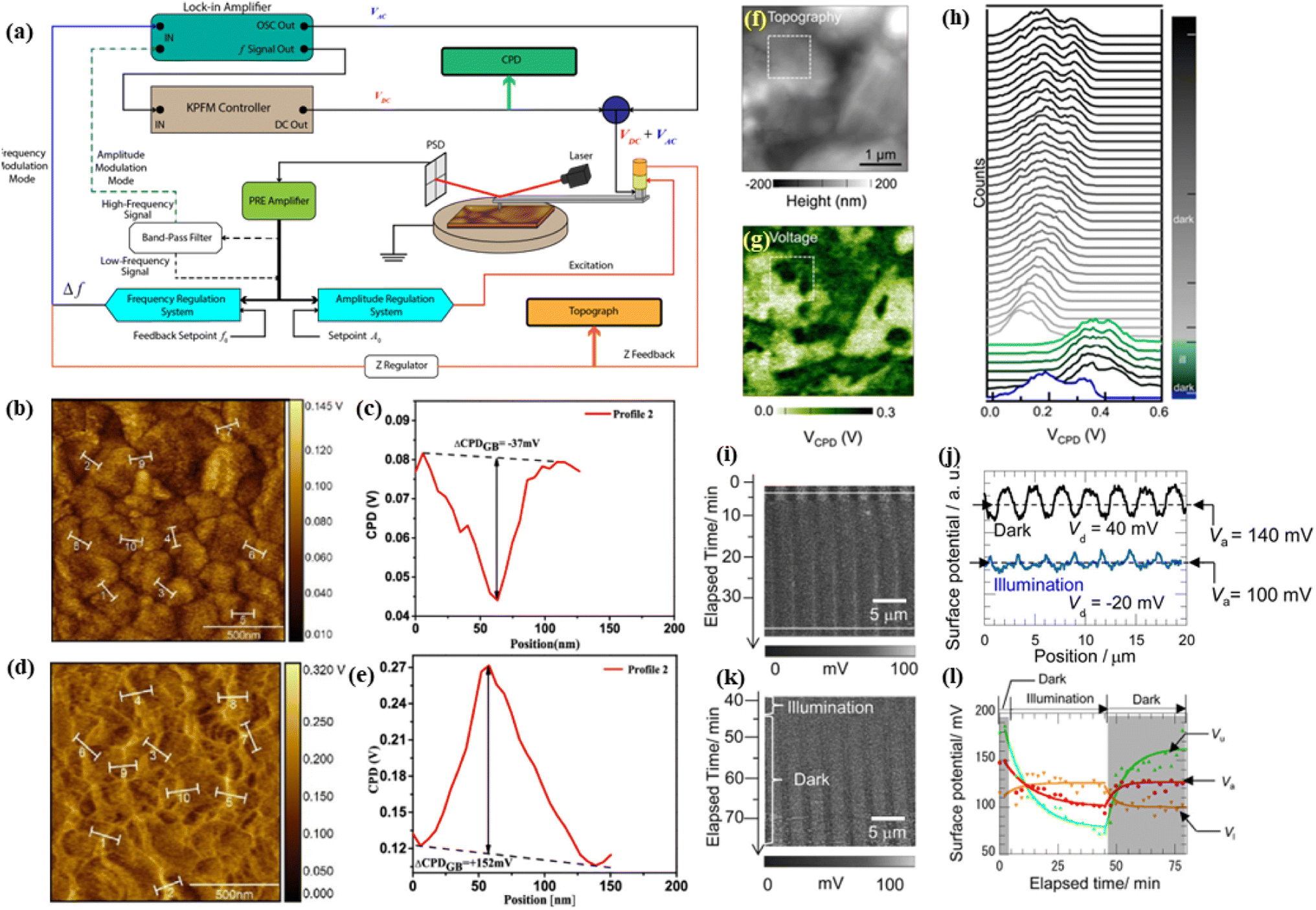 | ||
| Fig. 3 (a) Schematics of KPFM, (b) CPD mapping in dark conditions for the pristine perovskite, (c) individual line profiles for CPD variation between the GB and the adjacent grain surface (GS), (d) CPD mapping for the PHI-treated perovskite, (e) CPD variation between GB and the adjacent GS of the PHI-treated perovskite.77 Reproduced from ref. 77 with permission from the American Chemical Society, copyright 2020. Surface potential evolution of the perovskite at the nanoscale, (f) surface topography, (g) voltage acquired through KPFM measurement in the dark for the selected area in (f). (h) The voltage distribution as a function of time showing reversible dynamics for dark scans.78 Reproduced from ref. 78 with permission from the American Chemical Society, copyright 2017. (i) KPFM images of the VCz(CHO)/PCBM film grating, (j) profiles of (i) under dark and illumination conditions, (k) KPFM image of the grating after light was turned off. (l) Surface potential against elapsed time in the upper and lower regions of the grating.79 Reproduced from ref. 79 with permission from the American Chemical Society, copyright 2014. | ||
The investigation of the SCG strategy was also extended to suppress the surface and GB defects via the insertion of phenyl hydrazinium iodide (PHI). In particular, the PHI-facilitated synergistic treatment reduced the current at the GBs while generating an electron barrier and reducing trap state density, which indicated the mitigated carrier recombination and leakage pathways, through GB passivation.77 The surface potential mapping results were taken at ten different (random) locations in the topography of the triple-cation perovskite to measure and differentiate the surface current from the current at GBs. Fig. 3b–d represent the surface potential images of the pristine and PHI-treated perovskite layers, respectively, and Fig. 3c–e represent the CPD variation between the GB and GS for the pristine and PHI-modified perovskites obtained through line profiles at different locations.77 For the pristine perovskite, the GBs exhibited negative potential as compared to the GS, and the average value of the potential difference (ΔCPDGB = CPDGB − CPDGS) observed at 10 different areas was −35.68 mV, indicating a negative potential barrier or a hole barrier at the GBs. The PHI-treated perovskite showed the opposite behavior, i.e., the CPD at the GB was positive as compared to the adjacent GS, which is attributed to the effective PHI passivation.77 High-speed scans (16 s/scan) over the perovskite sample surface under illumination-, and dark-KPFM at the nanoscale spatial resolution of 50 nm were reported by Leite et al.78 As represented in Fig. 3f–h, the topography of the perovskite sample with the simultaneously scanned voltage over a selected area was obtained under dark-KPFM measurements. Fig. 3j represents the statistical analyses for the quantification of CPD measurements over perovskites tested in their study, as the histograms depict that the initial distribution of dark voltage (blue) is relatively wide, with a peak at approximately 0.2 V. Upon exposure to light, this distribution shifts, with the peak increasing to around 0.4 V (shown by the green curves). Over time, VCPD widened again, predominantly extending towards higher voltages (dark gray curves). This pattern persisted across various illumination intensities applied to the perovskite, ranging from 2.0 nW to 4.2 mW. These KPFM-based measurements highlight the temporal evolution of voltage in the perovskite following exposure to light, even under dark conditions.78 In another recent study regarding surface potential measurement through KPFM, an effective organo-metallic-functionalized interface was reported for high performance and improved operational stability of inverted PSCs. The perovskite film treated with optimized ferrocenyl-bis-thiophene-2-carboxylate (FcTc2) demonstrated a reduced contact potential of approximately 50 mV as compared to the control sample that implies a direct interaction and surface charge transfer between FcTc2 and the perovskite semiconductor. Furthermore, the FcTc2-functionalized perovskite exhibited a narrower potential distribution and surface potential difference, approximately 150 mV, in contrast to the control sample, which showed a difference of approximately 250 mV. This uniform distribution of surface contact potential is advantageous for facilitating efficient charge carrier extraction and preventing non-radiative recombination.71 The surface reconstruction strategy within the PSC domain has been reported several times as another unique approach to engineering the overall device performance and operational stability of single-junction organometallics, lead, and tin-based PSCs, and large-area tandem cells.80–84 Evaluating the surface potential through KPFM may provide extended evidence for the extent to which the actual reconstruction is executed and the improved photodynamics would be tested simultaneously.
OSCs consisting of a conjugated polymer/fullerene bulk heterojunction were evaluated for the first time (to the best of our knowledge) by Hoppe and co-workers through KPFM against the topography and local work functions at the nm scale.70 Surface analyses of two distinct kinds of film obtained through the chlorobenzene and toluene-based casting of the classical organic solar cell system with MDMO-PPV/PCBM blends were conducted, and KPFM-enhanced findings enabled them to identify the electron transmission barrier at the PCBM/cathode interface. The said barrier was found to be responsible for the lower PCE in their final OSC devices synthesized from toluene casting in comparison to chlorobenzene-based casting.70 Pump-probe KPFM was reported to reveal the hidden surface photovoltages (SPV) in the organic bulk heterojunction thin film based on the PTB7-PC71BM tandem OSCs.85 Two-dimensional dynamic maps of the organic blend's photo-response were tested by recording pump-probe KPFM curves in data cube mode. These maps revealed regions with an additional positive SPV component, showing decay time constants of several tens of microseconds. Decay time constant images of the negative SPV component confirmed that the acceptor clusters serve as electron-trapping sites. The revealing of SPV in organic blends showed strong implications over other thin film PV devices for a better understanding of crucial aspects of surface-enhanced potentials.85 Watanabe et al. reported an in situ KPFM study to identify the electron donor and acceptor regions within blended organic thin films.79 Periodic photopolymerization, triggered by an interference pattern from two laser beams, created surface relief gratings (SRGs) in the structured films. Analysis of the surface potential distribution within the SRGs suggests the formation of donor and acceptor spatial distributions. Illumination induced reversible changes in the surface potential due to the generation of fullerene anions and hole transport from the films to substrates, demonstrating the successful imaging of the local photovoltaic characteristics of the structured photovoltaic devices. Fig. 3i and j represent KPFM images taken under illumination and dark conditions for the VCz(CHO)/PCBM film (80![[thin space (1/6-em)]](https://www.rsc.org/images/entities/char_2009.gif) :20 wt%) grating. During the first observation at 3 min, the KPFM image revealed periodic surface potential modulation based on the distribution of donor and acceptor materials in the films and the depth of this modulation was approximately 40 mV. KPFM images exhibited changes in the surface potential distribution post-illumination, as after 40 minutes, the surface potential of the upper region decreased relative to the lower region, resulting in a saturated potential modulation of approximately −20 mV. Fig. 3k represents the KPFM image of the grating after the white light was switched off, demonstrating a gradual return of the surface potential distribution to its pre-illuminated state. This reversibility highlights the processes of charge carrier generation under illumination and subsequent charge carrier collection. The periods of charging and discharging are notably longer than the intervals of photoinduced charge generation, suggesting the presence of deep electron charge trapping and de-trapping. These phenomena are observable in both the surface potential of the upper and lower regions of the gratings, as well as the average surface potential as demonstrated by Fig. 3l. Local PV properties evaluated by KPFM under monochromatic light illumination enabled the acquisition of photocurrent action spectra in the structured organic blended film SRGs synthesized through the periodic photopolymerization.79
:20 wt%) grating. During the first observation at 3 min, the KPFM image revealed periodic surface potential modulation based on the distribution of donor and acceptor materials in the films and the depth of this modulation was approximately 40 mV. KPFM images exhibited changes in the surface potential distribution post-illumination, as after 40 minutes, the surface potential of the upper region decreased relative to the lower region, resulting in a saturated potential modulation of approximately −20 mV. Fig. 3k represents the KPFM image of the grating after the white light was switched off, demonstrating a gradual return of the surface potential distribution to its pre-illuminated state. This reversibility highlights the processes of charge carrier generation under illumination and subsequent charge carrier collection. The periods of charging and discharging are notably longer than the intervals of photoinduced charge generation, suggesting the presence of deep electron charge trapping and de-trapping. These phenomena are observable in both the surface potential of the upper and lower regions of the gratings, as well as the average surface potential as demonstrated by Fig. 3l. Local PV properties evaluated by KPFM under monochromatic light illumination enabled the acquisition of photocurrent action spectra in the structured organic blended film SRGs synthesized through the periodic photopolymerization.79
Multimodal c-AFM can also be extended to observe the charge recombination and transport constants (τr, τt) through TPV and TPC to establish the collection efficiency of photogenerated charge carriers. The time constants were calculated through TPV and TPC measurements under open- and short-circuit conditions.77,86 Many studies have been supported by the c-AFM nanoscale mapping of the OSCs where the charge carrier dynamics of the control and the optimized OSCs have been compared. As explained in the introduction, OSCs are comprised of blends of organic donor and acceptor regions, unlike GBs, and locating and differentiating such regions is the obvious advantage of the multimodal AFM technique. Lu et al.60 improved the performance of widely used PM6:Y6-based OSCs from 16.2% to 17.6% by employing highly emissive trans-bis(dimesitylboron) stilbene (BBS) as a solid additive. The c-AFM nanoscale mapping declared that the revised PM6: Y6: BBS device has a longer charge-carrier τr, shorter charge-carrier τt, and improved charge-carrier LD. These results indicate that the performance improvement is mainly derived from the enhanced exciton dissociation and charge-transport ability. The fine-tuning of another organic semiconductor PBDB-T: PNDI-CBS0.5 after annealing showed enhanced charge carrier dynamics, resulting in overall enhanced photovoltaic performance.87 Wang et al.88 found that PTB7-Th: Y6 QHJ devices at donor: acceptor (D°:°A) ratios of 1:8 or 1:20 can achieve 95% or 64% of the efficiency obtained from its BHJ counterpart at the optimal D:A ratio of 1:1.2. Yu et al.89 concluded that PDI-EH benefits the photovoltaic performance of ternary OSCs under both 1-sun and indoor illuminations due to morphology modulation and the resulting local charge carrier dynamics. c-AFM nanoscale mapping for OSCs is more complicated than for PSCs. Unlike PSCs, which mainly focus on the perovskite GB locations, OSCs have blend films with different D°:°A ratios and it is harder to localize the mapping area. During the nanoscale mapping of OSCs, the donor-, and acceptor-rich regions are compared, while for mapping PSCs, the grains and GB locations can be clearly identified and compared. The c-AFM setup is made to selectively detect the electron current by using the inverted device architecture of the samples and incorporating an electron-transport layer (like ZnO or PTAA, etc.) between the active layer and bottom ITO/FTO electrode. In the c-AFM surface conductivity images, the greater conductive region can be assigned as the acceptor-rich region, whereas the lesser conductive region can be assigned as the donor-rich region in most cases.87,90 However, in some cases, the ambipolar charge transport channel from the OSCs can affect the electron transport and result in unusual donor-rich and acceptor-rich region assignments. Also, once the donor or acceptor ratio is extremely higher than the other, the acceptor-rich or donor-rich regions may not be identified.88 One of the most recent contact mode c-AFM-enhanced nanoscale mappings in OSCs for the concurrent and quantitative analysis of carrier dynamics was performed by our group. To explain the favorable results, by employing highly emissive BBS as an additive into PM6:Y6-based OSCs, the carriers' transient parameters such as τt, τr, and LD were compared at the neighboring donor-rich and acceptor-rich regions in the active layer. Fig. 4a and b shows the 1 μm × 1 μm contact mode AFM topography of PM6:Y6 and PM6:Y6: BBS films.60 The mapping area (100 nm × 100 nm) indicated by the red square was selected from the half-bright (acceptor-rich region) and half-dark (donor-rich region) of the OSCs' c-AFM conductivity images in Fig. 4c and d. Fig. 4e–g presents the nanoscale τt, τr, and LD mapping of both PM6:Y6 and PM6:Y6: BBS samples in comparison within the red square. The donor-rich and acceptor-rich regions are both split by white dashed lines in each mapping.60 The work indicated that the modified PM6:Y6: BBS sample has an extended mean τr (4.94 ± 0.39 μs) as compared to that of PM6:Y6 (τr = 4.70 ± 0.31 μs). The mean τt is shorter in the BBS-based sample (τt = 4.52 ± 0.28 μs) than that of PM6:Y6 (τt = 4.67 ± 0.38 μs). In line with eqn (3), the mean LD for the PM6:Y6: BBS sample was 68.2 ± 3.9 nm, which is longer than that of the PM6:Y6 sample (65.4 ± 3.1 nm). These transient parameter improvements are beneficial to the charge carrier dynamics and photovoltaic performance. On the other hand, the donor-rich regions showed higher LD, which is desirable for increased bimolecular recombination. Fig. 4h and i describes the statistical view from the histogram distribution of the three transient parameters. The majority of τr values (86.6%) of the PM6:Y6 sample were less than 4.8 μs, while most τr values (44.2%) of the PM6:Y6: BBS sample were more than 4.95 μs. The τr values of both samples are close, between 4.5 and 4.7 μs, but PM6:Y6: BBS had only 2.7% τr values > 4.9 μs while PM6:Y6 had 11.8%. Further examination concluded that the sample without BBS had only 15.9% of LD values >67.5 nm, while 36.3% of LD > 67.5 nm in BBS-based samples. The LD mapping and histogram indicate that the addition of BBS can effectively increase the charge-carrier LD of the organic active layer.60 These measurements provide another route to verify the carrier transport and collection mechanism at the respective electrode, which is directly related to the photodynamics (dis)order of the PSC and OSC devices.77,91
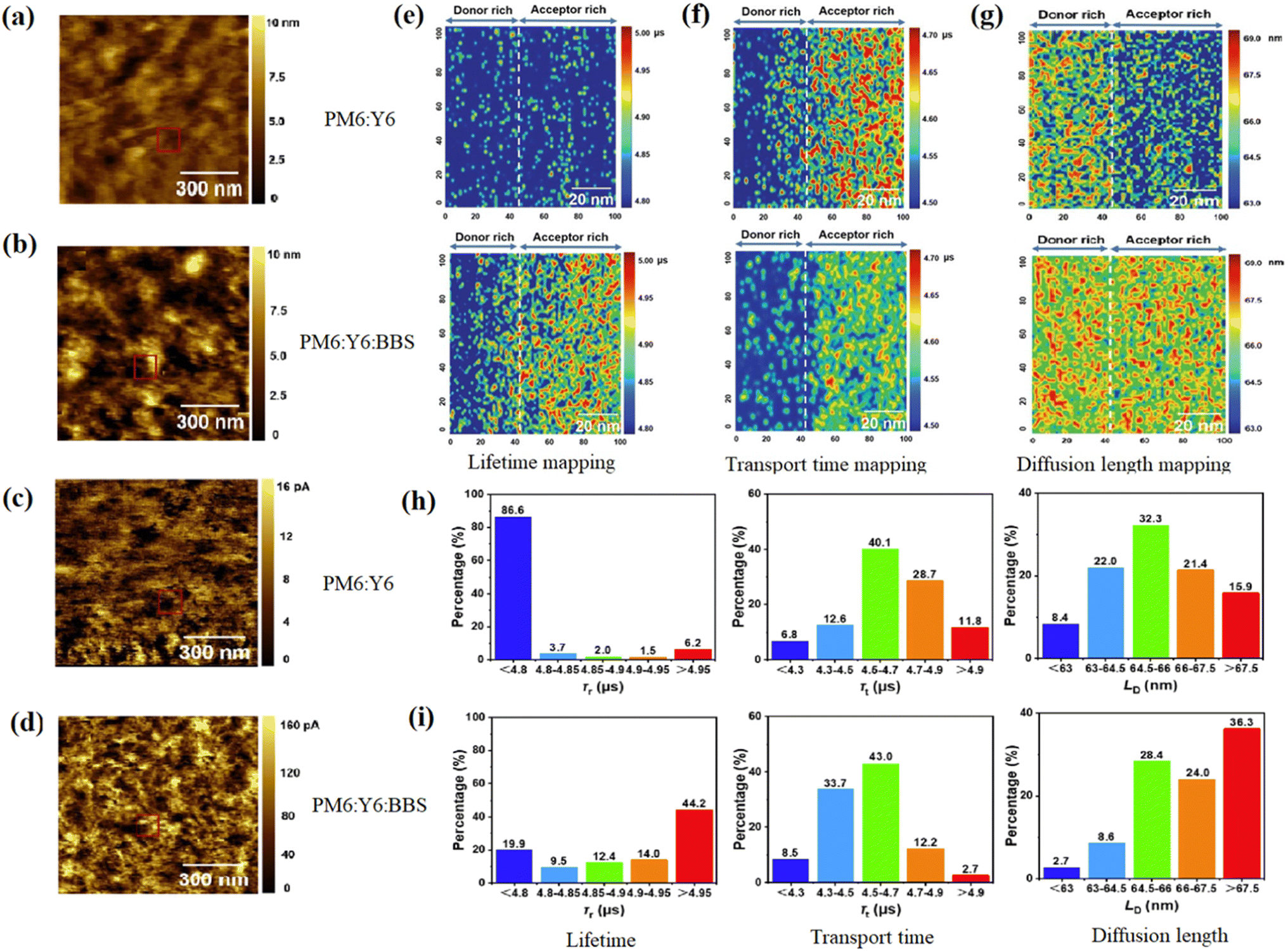 | ||
| Fig. 4 AFM-topography of (a) PM6:Y6, and (b) PM6:Y6: BBS. c-AFM-conductivity of (c) PM6:Y6 and (d) PM6:Y6: BBS. (e) Carrier lifetime ‘τr’, (f) carrier transport time ‘τt’, (g) carrier diffusion length LD. (h and i) Statistical distribution of τr, τt, and LD for PM6:Y6 and PM6:Y6: BBS organic films.60 Reproduced from ref. 60 with permission from John Wiley and Sons, copyright 2022. | ||
The photodynamics of single-junction conventional PSCs with active layer thicknesses of several nanometers have been reported many times with nanoscale mapping as a characteristic tool. The fabrication of a tandem c-Si/PSC solar cell device was reported with the PAL thickness in microns as a wide-bandgap top cell, and the photodynamics of the corresponding perovskite was studied through a nanoscale mapping technique. Hou et al. reported the enhanced LD and efficient carrier collection through engineering micrometer (μm)-thick PAL with a self-limiting passivant (SLP) of 1-butanethiol. A concentrated solution (1.65–1.75 M) of perovskite was used to fully cover the pyramid-type c-Si textured surface of the underside with micron thickness, a crystalline grain size of 4 μm, and comparatively reduced GBs. Nanoscale mapping was carried out to investigate the AFM topography of the wide-bandgap Cs0.05MA0.15FA0.8PbI2.25Br0.75 perovskite, with the charge carrier LD measurements. Characterized by nanoscale spatial mapping in c-AFM mode, the carrier LD in the SLP-treated sample in the grains and GBs was improved as compared to the control sample. Fig. 5a–c represents the nanoscale mapping of the corresponding μm-thick wide-band perovskite, as the carriers LD within the grains for the SLP-treated sample was around 570 nm and about 50 nm in GBs (the region denoted by the blue-square and confined by the white dashed-lines), while the carrier LD was decreased by 100 nm in the pristine samples. By the synergistic GB passivation and mitigation of phase-segregation through the SLP approach, the final solar cell device (with tandem architecture as shown in Fig. 5d) with c-Si/μm-thick wide-band perovskite (Fig. 5e) yielded a certified (Fraunhofer ISE CalLab PV-cell) PCE of 25.7%, as represented in Fig. 5f.92 The nanoscale spatial mapping has unique features, including the measurement of transient photodynamics parameters such as τr, τt, and LD, combined with VCPD at the grain surface and GBs by KPFM, so the mapping technique has strong potential for investigating the large-area perovskite thin film coatings deposited by the slot-die-coating, inkjet printing, gravure, or relief-printing,93etc.
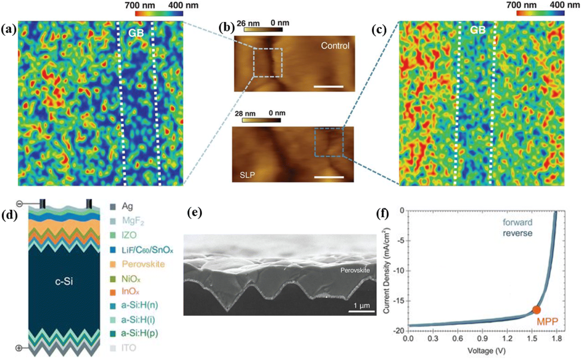 | ||
| Fig. 5 (a) Nanoscale mapping of the area indicated by the light blue square in (100 × 100 nm) of the diffusion length of the control perovskite. The white dashed line shows the GB region. (b) c-AFM topography of the control sample (top) and SLP perovskite (bottom) (scale bar-100 nm). (c) Nanoscale-resolved mapping of the area indicated by the dark blue square in (b) of LD of the SLP perovskite. The white dashed line shows the corresponding GB region. (d), (e) Ultra-thick perovskite absorber deposited on top of Si by solution processing. (f) JV curve for the certified cells modified through the SLP approach.92 Reproduced from ref. 92 with permission from The American Association for the Advancement of Science, copyright 2020. | ||
Limitations
There are some limitations to the nanoscale mapping of charge carrier dynamics, including the spatial resolution restriction of the tiny morphological features in AFM (Agilent 5500), as quantum dots (QDs) with diameters smaller than 5 nm are hard to identify and locate for nanoscale mapping. Due to the limitation of the laser generator sources (with a 402 nm violet laser pulse, 473 nm blue laser pulse, and the mostly used 532 nm green laser pulse), the solar cells with low absorbance at those wavelengths might not work for nanoscale mapping since irregular current pulses cause greater uncertainty for fitting. However, this limitation can be addressed with a continuum laser generator with a wider range. Nanoscale mapping at high resolution can be advantageous for the better investigation and understanding of carrier dynamics in perovskite and blended organic photoactive layers, which may provide a facile way to improve the photovoltaic performance in the respective devices.Summary and outlook
Multimodal nanoscale spatial and time-resolved mapping of photoinduced charge carriers are crucial for the device performance and operational stability of PSC and OSC devices. The benefits of the multimodal nanoscale mapping technique are manifold, however, reports regarding the large-area solar modules and their extremely important carrier dynamics through such a technique are still lacking. The current status of the research on PSC and OSC devices demands thorough investigation i.e., from the structure to the properties, and multimodal techniques are required to engineer the photovoltaic yields and improve the intrinsic stability of such devices. Within the PSC research domain, all-inorganic perovskite solar cells have comparatively higher thermal and operational stability and would be the best possible research direction to yield higher throughputs via nanoscale engineering. These nanoscale multimodal approaches should be integrated into the manufacturing lines according to set industrial protocols to gain ultrahigh outputs. The prospect of the nanoscale mapping as a multimodal approach also includes the integration of a variety of thin film morphologies and optoelectronic devices, such as nanowire-based OSCs, wrinkling PSCs, perovskite and organic light emitting diodes, large area PSCs, and their tandem partners, using different laser wavelengths at higher resolutions.Author contributions
MBF and YZ conceived the idea and wrote the outline and final draft. QQ supervised the project and revised the draft through its final format. All authors revised the draft.Conflicts of interest
We have a patent related to this work, (Patent No. US 11016118B2, May, 2021) for our multimodal technique. The authors declare no competing interests.Acknowledgements
This work is supported by the startup funding for faculty from Syracuse University.References
- J. Hou, O. Inganäs, R. H. Friend and F. Gao, Nat. Mater., 2018, 17, 119–128 CrossRef CAS PubMed.
- S. Guan, Y. Li, C. Xu, N. Yin, C. Xu, C. Wang, M. Wang, Y. Xu, Q. Chen, D. Wang, L. Zuo and H. Chen, Adv. Mater., 2024, 2400342 CrossRef PubMed.
- Y. Zhang, W. Deng, C. E. Petoukhoff, X. Xia, Y. Lang, H. Xia, H. Tang, H. T. Chandran, S. Mahadevan and K. Liu, Joule, 2024, 8, 509–526 CrossRef CAS.
- S. Yang, Y. Liu, X. Lian and J. Chu, Joule, 2022, 6, 2248–2250 CrossRef.
- G.-H. Kim and D. S. Kim, Joule, 2021, 5, 1033–1035 CrossRef.
- S. Foo, M. Thambidurai, P. Senthil Kumar, R. Yuvakkumar, Y. Huang and C. Dang, Int. J. Energy Res., 2022, 46, 21441–21451 CrossRef CAS.
- K. Wang, S. Olthof, W. S. Subhani, X. Jiang, Y. Cao, L. Duan, H. Wang, M. Du and S. F. Liu, Nano Energy, 2020, 68, 104289 CrossRef CAS.
- P. K. Nayak, S. Mahesh, H. J. Snaith and D. Cahen, Nat. Rev. Mater., 2019, 4, 269–285 CrossRef CAS.
- L. K. Reb, M. Böhmer, B. Predeschly, S. Grott, C. L. Weindl, G. I. Ivandekic, R. Guo, C. Dreißigacker, R. Gernhäuser and A. Meyer, Joule, 2020, 4, 1880–1892 CrossRef CAS.
- J. Wu, H. Cha, T. Du, Y. Dong, W. Xu, C. T. Lin and J. R. Durrant, Adv. Mater., 2022, 34, 2101833 CrossRef CAS PubMed.
- X. Guo, N. Zhou, S. J. Lou, J. Smith, D. B. Tice, J. W. Hennek, R. P. Ortiz, J. T. L. Navarrete, S. Li and J. Strzalka, Nat. Photon., 2013, 7, 825–833 CrossRef CAS.
- M. A. Green, A. Ho-Baillie and H. J. Snaith, Nat. Photon., 2014, 8, 506–514 CrossRef CAS.
- D. Zheng, F. Raffin, P. Volovitch and T. Pauporté, Nat. Commun., 2022, 13, 6655 CrossRef CAS.
- C. He and X. Liu, Light: Sci. Appl., 2023, 12, 15 CrossRef CAS PubMed.
- L. Shi, Z. Yang, Y. Zhang, Z. Ai, Y. Bao, T. Ma, L. Qin, G. Cao, C. Wang and X. Li, Sol. RRL, 2024, 8, 2300752 CrossRef CAS.
- J. Shi, Y. Li, Y. Li, D. Li, Y. Luo, H. Wu and Q. Meng, Joule, 2018, 2, 879–901 CrossRef CAS.
- J. R. Bautista-Quijano, O. Telschow, F. Paulus and Y. Vaynzof, Chem. Commun., 2023, 59, 10588–10603 RSC.
- T. P. van der Pol, K. Datta, M. M. Wienk and R. A. Janssen, Adv. Opt. Mater., 2022, 10, 2102557 CrossRef CAS.
- T. Kirchartz, J. A. Márquez, M. Stolterfoht and T. Unold, Adv. Energy Mater., 2020, 10, 1904134 CrossRef CAS.
- M. List, J. Faisst, F. Heinz and U. Würfel, Adv. Opt. Mater., 2023, 11, 2300895 CrossRef CAS.
- D. Garratt, L. Misiekis, D. Wood, E. W. Larsen, M. Matthews, O. Alexander, P. Ye, S. Jarosch, C. Ferchaud and C. Strüber, Nat. Commun., 2022, 13, 3414 CrossRef CAS PubMed.
- A. M. El-Zohry, B. Turedi, A. Alsalloum, P. Maity, O. M. Bakr, B. S. Ooi and O. F. Mohammed, Commun. Chem., 2022, 5, 67 CrossRef CAS PubMed.
- J. Yu, Y. Xing, Z. Shen, Y. Zhu, D. Neher, N. Koch and G. Lu, Mater. Horiz., 2021, 8, 1461–1471 RSC.
- B. Qiu, S. Chen, C. Sun, J. Yuan, X. Zhang, C. Zhu, S. Qin, L. Meng, Y. Zhang and C. Yang, Sol. RRL, 2020, 4, 1900540 CrossRef CAS.
- L. Tong, J. Yuan, Z. Zhang, J. Tang and Z. Wang, Nat. Nanotechnol., 2023, 18, 145–152 CrossRef CAS.
- F. M. Alcorn, P. K. Jain and R. M. van der Veen, Nat. Rev. Chem, 2023, 7, 256–272 CrossRef CAS.
- M. A. Almajhadi, S. M. A. Uddin and H. K. Wickramasinghe, Nat. Commun., 2020, 11, 5691 CrossRef CAS PubMed.
- J. Kong, R. Giridharagopal, J. S. Harrison and D. S. Ginger, J. Phys. Chem. Lett., 2018, 9, 3307–3314 CrossRef CAS PubMed.
- J. Zeng, Y. Dong, J. Zhang and J. Wang, J. Opt., 2023, 023001 CrossRef.
- K. L. Gu, Y. Zhou, W. A. Morrison, K. Park, S. Park and Z. Bao, ACS Nano, 2018, 12, 1473–1481 CrossRef CAS PubMed.
- H. Robert, Nat. Commun., 2021, 12, 361 CrossRef.
- A. Phani, H. S. Jung and S. Kim, Commun. Phys., 2021, 4, 72 CrossRef.
- S. D. Stranks, Matter, 2021, 4, 3852–3866 CrossRef CAS.
- D. W. de Quilettes, S. M. Vorpahl, S. D. Stranks, H. Nagaoka, G. E. Eperon, M. E. Ziffer, H. J. Snaith and D. S. Ginger, Science, 2015, 348, 683–686 CrossRef CAS PubMed.
- S. Macpherson, T. A. Doherty, A. J. Winchester, S. Kosar, D. N. Johnstone, Y.-H. Chiang, K. Galkowski, M. Anaya, K. Frohna and A. N. Iqbal, Nature, 2022, 607, 294–300 CrossRef CAS.
- M. V. Khenkin, A. KM, I. Visoly-Fisher, S. Kolusheva, Y. Galagan, F. Di Giacomo, O. Vukovic, B. R. Patil, G. Sherafatipour and V. Turkovic, ACS Appl. Energy Mater., 2018, 1, 799–806 CrossRef CAS.
- P. Gratia, I. Zimmermann, P. Schouwink, J.-H. Yum, J.-N. Audinot, K. Sivula, T. Wirtz and M. K. Nazeeruddin, ACS Energy Lett., 2017, 2, 2686–2693 CrossRef CAS.
- S. Y. Leblebici, L. Leppert, Y. Li, S. E. Reyes-Lillo, S. Wickenburg, E. Wong, J. Lee, M. Melli, D. Ziegler and D. K. Angell, Nat. Energy, 2016, 1, 1–7 Search PubMed.
- J. Song, Y. Zhou, N. P. Padture and B. D. Huey, Nat. Commun., 2020, 11, 3308 CrossRef CAS PubMed.
- Z. Chu, M. Yang, P. Schulz, D. Wu, X. Ma, E. Seifert, L. Sun, X. Li, K. Zhu and K. Lai, Nat. Commun., 2017, 8, 2230 CrossRef PubMed.
- T. S. Sherkar, C. Momblona, L. Gil-Escrig, J. Avila, M. Sessolo, H. J. Bolink and L. J. A. Koster, ACS Energy Lett., 2017, 2, 1214–1222 CrossRef CAS PubMed.
- G. E. Eperon and D. S. Ginger, Nat. Energy, 2016, 1, 1–2 Search PubMed.
- W. Bao, M. Melli, N. Caselli, F. Riboli, D. S. Wiersma, M. Staffaroni, H. Choo, D. Ogletree, S. Aloni and J. Bokor, Science, 2012, 338, 1317–1321 CrossRef CAS PubMed.
- X. Xiao, W. Li, Y. Fang, Y. Liu, Y. Shao, S. Yang, J. Zhao, X. Dai, R. Zia and J. Huang, Nat. Commun., 2020, 11, 2215 CrossRef CAS PubMed.
- J.-J. Li, J.-Y. Ma, Q.-Q. Ge, J.-S. Hu, D. Wang and L.-J. Wan, ACS Appl. Mater. Interfaces, 2015, 7, 28518–28523 CrossRef CAS PubMed.
- F. Wang, M. Li, Q. Tian, R. Sun, H. Ma, H. Wang, J. Chang, Z. Li, H. Chen and J. Cao, Nat. Commun., 2023, 14, 3216 CrossRef CAS PubMed.
- G. E. Eperon, D. Moerman and D. S. Ginger, ACS Nano, 2016, 10, 10258–10266 CrossRef CAS PubMed.
- S. Draguta, J. A. Christians, Y. V. Morozov, A. Mucunzi, J. S. Manser, P. V. Kamat, J. M. Luther and M. Kuno, Energy Environ. Sci., 2018, 11, 960–969 RSC.
- D. Sharma, N. Nicoara, P. Jackson, W. Witte, D. Hariskos and S. Sadewasser, Nat. Energy, 2024, 1–9 Search PubMed.
- P. De Pablo, F. Moreno-Herrero, J. Colchero, J. G. Herrero, P. Herrero, A. Baró, P. Ordejón, J. M. Soler and E. Artacho, Phys. Rev. Lett., 2000, 85, 4992 CrossRef CAS PubMed.
- Y. Kutes, Y. Zhou, J. L. Bosse, J. Steffes, N. P. Padture and B. D. Huey, Nano Lett., 2016, 16, 3434–3441 CrossRef CAS PubMed.
- W. J. Yin, T. Shi and Y. Yan, Adv. Mater., 2014, 26, 4653–4658 CrossRef CAS.
- K. P. McKenna, ACS Energy Lett., 2018, 3, 2663–2668 CrossRef CAS.
- A. J. Knight, J. Borchert, R. D. Oliver, J. B. Patel, P. G. Radaelli, H. J. Snaith, M. B. Johnston and L. M. Herz, ACS Energy Lett., 2021, 6, 799–808 CrossRef CAS PubMed.
- S. G. Motti, J. B. Patel, R. D. Oliver, H. J. Snaith, M. B. Johnston and L. M. Herz, Nat. Commun., 2021, 12, 6955 CrossRef CAS PubMed.
- Y. Yuan, G. Yan, C. Dreessen, T. Rudolph, M. Hülsbeck, B. Klingebiel, J. Ye, U. Rau and T. Kirchartz, Nat. Mater., 2024, 23, 391–397 CrossRef CAS PubMed.
- M. Saliba, T. Matsui, J.-Y. Seo, K. Domanski, J.-P. Correa-Baena, M. K. Nazeeruddin, S. M. Zakeeruddin, W. Tress, A. Abate and A. Hagfeldt, Energy Environ. Sci., 2016, 9, 1989–1997 RSC.
- B. Bahrami, A. H. Chowdhury, A. Gurung, S. Mabrouk, K. M. Reza, S. I. Rahman, R. Pathak and Q. Qiao, Nano Today, 2020, 33, 100874 CrossRef CAS.
- L. S. Pingree, O. G. Reid and D. S. Ginger, Adv. Mater., 2009, 21, 19–28 CrossRef CAS.
- H. Lu, K. Chen, R. S. Bobba, J. Shi, M. Li, Y. Wang, J. Xue, P. Xue, X. Zheng and K. E. Thorn, Adv. Mater., 2022, 34, 2205926 CrossRef CAS PubMed.
- C. Liu, Y. Yang, H. Chen, J. Xu, A. Liu, A. S. Bati, H. Zhu, L. Grater, S. S. Hadke and C. Huang, Science, 2023, 382, 810–815 CrossRef CAS PubMed.
- H. Kim, J. Lee, B. Kim, H. R. Byun, S. H. Kim, H. M. Oh, S. Baik and M. S. Jeong, Sci. Rep., 2019, 9, 15461 CrossRef PubMed.
- J. Van de Lagemaat and A. Frank, J. Phys. Chem. B, 2001, 105, 11194–11205 CrossRef CAS.
- J. Wei, Q. Wang, J. Huo, F. Gao, Z. Gan, Q. Zhao and H. Li, Adv. Energy Mater., 2021, 11, 2002326 CrossRef CAS.
- Z. Lin, M. C. Folgueras, H. K. Le, M. Gao and P. Yang, Matter, 2022, 5, 1455–1465 CrossRef CAS.
- M. B. Faheem, B. Khan, C. Feng, M. U. Farooq, F. Raziq, Y. Xiao and Y. Li, ACS Energy Lett., 2019, 5, 290–320 CrossRef.
- B. Chen, M. Yang, X. Zheng, C. Wu, W. Li, Y. Yan, J. Bisquert, G. Garcia-Belmonte, K. Zhu and S. Priya, J. Phys. Chem. Lett., 2015, 6, 4693–4700 CrossRef CAS PubMed.
- K. M. Reza, A. Gurung, B. Bahrami, A. H. Chowdhury, N. Ghimire, R. Pathak, S. I. Rahman, M. A. R. Laskar, K. Chen and R. S. Bobba, Sol. RRL, 2021, 5, 2000740 CrossRef CAS.
- T.-W. Zeng, F.-C. Hsu, Y.-C. Tu, T.-H. Lin and W.-F. Su, Chem. Phys. Lett., 2009, 479, 105–108 CrossRef CAS.
- H. Hoppe, T. Glatzel, M. Niggemann, A. Hinsch, M. C. Lux-Steiner and N. Sariciftci, Nano Lett., 2005, 5, 269–274 CrossRef CAS.
- Z. Li, B. Li, X. Wu, S. A. Sheppard, S. Zhang, D. Gao, N. J. Long and Z. Zhu, Science, 2022, 376, 416–420 CrossRef CAS.
- J. R. O'Dea, L. M. Brown, N. Hoepker, J. A. Marohn and S. Sadewasser, MRS Bull., 2012, 37, 642–650 CrossRef.
- Z. Cui, J. Sun, D. Landerer, C. Sprau, R. Thelen, A. Colsmann, H. Hölscher, W. Ma and L. Chi, Adv. Mater. Interfaces, 2016, 3, 1600446 CrossRef.
- E. M. Lanzoni, T. Gallet, C. Spindler, O. Ramirez, C. K. Boumenou, S. Siebentritt and A. Redinger, Nano Energy, 2021, 88, 106270 CrossRef CAS.
- J. Li, B. Huang, E. Nasr Esfahani, L. Wei, J. Yao, J. Zhao and W. Chen, npj Quantum Mater., 2017, 2, 56 CrossRef.
- Z. Zhao, X. Chen, H. Wu, X. Wu and G. Cao, Adv. Funct. Mater., 2016, 26, 3048–3058 CrossRef CAS.
- S. I. Rahman, B. S. Lamsal, A. Gurung, A. H. Chowdhury, K. M. Reza, N. Ghimire, B. Bahrami, W. Luo, R. S. Bobba and J. Pokharel, ACS Appl. Mater. Interfaces, 2020, 12, 41312–41322 CrossRef CAS PubMed.
- J. L. Garrett, E. M. Tennyson, M. Hu, J. Huang, J. N. Munday and M. S. Leite, Nano Lett., 2017, 17, 2554–2560 CrossRef CAS.
- S. Watanabe, Y. Fukuchi, M. Fukasawa, T. Sassa, A. Kimoto, Y. Tajima, M. Uchiyama, T. Yamashita, M. Matsumoto and T. Aoyama, ACS Appl. Mater. Interfaces, 2014, 6, 1481–1487 CrossRef CAS PubMed.
- X. Chu, Q. Ye, Z. Wang, C. Zhang, F. Ma, Z. Qu, Y. Zhao, Z. Yin, H.-X. Deng and X. Zhang, Nat. Energy, 2023, 8, 372–380 CrossRef CAS.
- H. Li, B. Chang, L. Wang, Z. Wang, L. Pan, Y. Wu, Z. Liu and L. Yin, ACS Energy Lett., 2022, 7, 3889–3899 CrossRef CAS.
- J. Zhuang, C. Liu, B. Kang, H. Cheng, M. Xiao, L. Li and F. Yan, Adv. Mater., 2023, 2309869 Search PubMed.
- X. Li, Z. Ying, J. Zheng, X. Wang, Y. Chen, M. Wu, C. Xiao, J. Sun, C. Shou and Z. Yang, Adv. Mater., 2023, 2211962 CrossRef CAS.
- J. He, J. Su, J. Di, Z. Lin, S. Zhang, J. Ma, J. Zhang, S. Liu, J. Chang and Y. Hao, Nano Energy, 2022, 94, 106960 CrossRef CAS.
- V. Aubriet, K. Courouble, O. Bardagot, R. Demadrille, Ł. Borowik and B. Grévin, Nanotechnology, 2022, 33, 225401 CrossRef CAS PubMed.
- E. M. Tennyson, B. Roose, J. L. Garrett, C. Gong, J. N. Munday, A. Abate and M. S. Leite, ACS Nano, 2018, 13, 1538–1546 Search PubMed.
- Y. Wu, S. Schneider, C. Walter, A. H. Chowdhury, B. Bahrami, H.-C. Wu, Q. Qiao, M. F. Toney and Z. Bao, J. Am. Chem. Soc., 2019, 142, 392–406 CrossRef PubMed.
- Y. Wang, M. B. Price, R. S. Bobba, H. Lu, J. Xue, Y. Wang, M. Li, A. Ilina, P. A. Hume and B. Jia, Adv. Mater., 2022, 34, 2206717 CrossRef CAS PubMed.
- T. Yu, F. Tintori, Y. Zhang, W. He, E. Cieplechowicz, R. S. Bobba, P. I. Kaswekar, M. Jafari, Y. Che and Y. Wang, J. Mater. Chem. A, 2023, 11, 5037–5047 RSC.
- M. Osaka, D. Mori, H. Benten, H. Ogawa, H. Ohkita and S. Ito, ACS Appl. Mater. Interfaces, 2017, 9, 15615–15622 CrossRef CAS PubMed.
- M. A. R. Laskar, W. Luo, N. Ghimire, A. H. Chowdhury, B. Bahrami, A. Gurung, K. M. Reza, R. Pathak, R. S. Bobba and B. S. Lamsal, Adv. Funct. Mater., 2020, 30, 2000778 CrossRef CAS.
- Y. Hou, E. Aydin, M. De Bastiani, C. Xiao, F. H. Isikgor, D.-J. Xue, B. Chen, H. Chen, B. Bahrami and A. H. Chowdhury, Science, 2020, 367, 1135–1140 CrossRef CAS PubMed.
- M. B. Faheem, B. Khan, J. Z. Hashmi, A. Baniya, W. Subhani, R. S. Bobba, A. Yildiz and Q. Qiao, Cell Rep. Phys. Sci., 2022, 3, 100827 CrossRef CAS.
Footnote |
| † These authors contributed equally to this work. |
| This journal is © The Royal Society of Chemistry 2024 |