
Research progress on two-dimensional indium selenide crystals and optoelectronic devices
Dan
Zheng
 ab,
Peng
Chen
ab,
Yi
Liu
ab,
Xing
Li
ab,
Kejing
Liu
ab,
Zi'ang
Yin
ab,
Riccardo
Frisenda
*d,
Qinghua
Zhao
*abc and
Tao
Wang
*abc
ab,
Peng
Chen
ab,
Yi
Liu
ab,
Xing
Li
ab,
Kejing
Liu
ab,
Zi'ang
Yin
ab,
Riccardo
Frisenda
*d,
Qinghua
Zhao
*abc and
Tao
Wang
*abc
aState Key Laboratory of Solidification Processing, Northwestern Polytechnical University, Xi'an, 710072, P. R. China
bKey Laboratory of Radiation Detection Materials and Devices, Ministry of Industry and Information Technology, Xi'an, 710072, P. R. China. E-mail: qinghua_zhao@nwpu.edu.cn; taowang@nwpu.edu.cn
cResearch & Development Institute of Northwestern Polytechnical University in Shenzhen, Shenzhen, 518063, P. R. China
dPhysics Department, Sapienza University of Rome, 00185 Rome, Italy. E-mail: riccardo.frisenda@uniroma1.it
First published on 31st May 2024
Abstract
Two-dimensional (2D) materials, with unique electronic properties, superior optoelectronic properties, and dangling-bond-free surfaces, have attracted significant attention and experienced rapid development both in fundamental science and for practical applications. Amid the plethora of 2D materials, indium selenide (InSe) has emerged as a promising candidate for future high-mobility optoelectronic devices. Nobel Prize laureate Andre Geim even describes it as “the ‘golden middle’ between silicon and graphene”. Over the past decade, remarkable findings and progress have been made in the fabrication of 2D InSe crystals and their application in devices, motivating us to delve deeply into these forefront developments. In this review, the physical properties such as the crystalline structure, band structure, and photoluminescence characteristics are discussed first. Then, the advancements in terms of synthesis techniques, characteristics and synthesis schemes in the fabrication of 2D InSe are summarized. Subsequently, the mechanisms of optimized strategies and recent progress in field effect transistors (FETs) as well as photodetectors based on this material are summarized, also highlighting the promising applications of 2D InSe in sensors and memory. Finally, an outlook, challenges and potential future research directions in the fabrication of 2D InSe and its devices are presented, such as large-scale fabrication without defect to integrate more devices, a variety of physical and chemical properties are regulated by doping or modification to broaden applications, improving the contact interface between the 2D materials and each layer of the stacking hetero interface to enhance the performance of devices, and designing multifunctional devices for future advanced optoelectronic devices as well as sensors, flexible, and wearable/portable electronic devices.
 Riccardo Frisenda | Riccardo Frisenda received his BSc and MSc degrees in physics from La Sapienza University in Rome, Italy, and his PhD in molecular electronics from the Technical University of Delft. He is currently working at La Sapienza University. His research interests include nanoscale transport, the electronic and optoelectronic properties of 2D materials, and the physics of devices based on these materials. |
 Qinghua Zhao | Qinghua Zhao is a full professor at Northwestern Polytechnical University (NWPU). He earned his doctoral degree in condensed matter physics from the Autonomous University of Madrid in Spain in 2020. After completing his PhD, he joined Andres Castellano-Gomez's Group as a Post-Doctoral Researcher. Currently, he serves as a professor at NWPU. His research interests focus on the design, construction, and performance optimization of novel two-dimensional electronic and optoelectronic devices. |
 Tao Wang | Tao Wang is a full professor at Northwestern Polytechnical University (NWPU) and serves as the deputy director of the Ministry of Industry and Information Technology Key Laboratory for Radiation Detection Materials and Devices. He received his PhD in materials science from NWPU in 2008. After earning his PhD, he joined NWPU as a Post-Doctoral Researcher in 2010 and has continued his work there to date. His research interests include crystal growth and device fabrication of compound semiconductors, the design and fabrication of novel radiation detection materials, and the exploration of new methods in crystal growth. |
1 Introduction
Moore's law, a pivotal guiding principle in modern electronics, guided the shrinking of the size of transistors and the increase in performances while simultaneously reducing the cost of silicon-based devices. Such a principle has inspired persistent efforts to downscale process nodes, ultimately leading to an exponential increase in the number of transistors on semiconductor chips.1,2 However, the physical limits of size reduction for conventional metal-oxide-semiconductor field effect transistors (MOSFETs) are approaching swiftly. In fact, Moore's law is no longer valid at sub-nanoscale channel width due to the physical limits of bulk materials.3 The rise of the short-channel effect has led to an escalation in off-state leakage current, contributing to challenges such as excessive static power consumption and heat dispersion. Consequently, there is a pressing need for innovative materials to enhance the existing Si-based metal-oxide-semiconductor technology, particularly to bolster gate voltage control under ultra-short channel size, essential for fulfilling future demands.To enable the diversification of electronics and their applications, novel technologies must be developed in the semiconductor industry.3 A standout feature of two-dimensional materials is the absence of dangling bonds in their basal planes, which makes it possible to overcome the traditional transistor scaling constraints. Graphene is a prototypical two-dimensional material and is considered to be one of the most promising materials for fabrication and application of next-generation electronic devices.4 However, graphene transistors cannot achieve a true “off” state (where the current flowing is close to zero) because of the absence of an inherent band gap, which restricts its application in the field of electronics and optoelectronics. In response to these constraints, researchers have embarked on a quest for innovative materials that exhibit similar structures and complimentary features to overcome the limitations of graphene. Transition metal dichalcogenides (TMDs), black phosphorus (BP), and an assortment of two-dimensional (2D) semiconductor materials have been proposed as candidates to bridge this chasm. Thanks to 2D materials with diverse band gap structures, unique electronic and optoelectronic device design has made breakthrough achievements in the device performance improvement, structural simplification and functional diversity.5 Indium selenide (InSe) is a particularly prominent member in the 2D materials family. Few-layer InSe has a hexagonal structure with a band gap of 1.3 eV, exhibits exceptional prowess in electrical transport and photoelectric conversion efficiency, and possesses distinct mechanical properties. Hailed by 2010 Nobel Prize laureate Andre Geim as the ‘golden middle’ between silicon and graphene, it is anticipated to have a substantial influence on the advancement of electronics and optoelectronics.6
This review primarily focuses on the key milestones in the development of 2D InSe materials' fundamental properties, fabrication techniques, and device applications over the past decade. First, a brief discussion is provided regarding the fundamental characteristics of InSe, encompassing its crystal structure, band structure and photoluminescence characteristics. Then the diverse avenues of material preparation and synthesis methods dedicated to layered InSe are navigated. Additionally, advanced applications such as field effect transistors, optoelectronic devices, and their optimized strategies are analyzed in detail. Furthermore, potential applications in mechanical sensing, gas sensing and medical diagnostics are briefly outlined (Fig. 1). Ultimately, an outlook, and the ongoing challenges are highlighted and the potential schemes to address them are envisioned for enhancing the performance of InSe materials and devices.
 | ||
| Fig. 1 Schematic illustration of several key features including basic properties, fabrication methods and application for 2D InSe materials. | ||
2 InSe fundamental properties
2.1 Crystal structure
The study of the InSe crystal and the multiple phase structure has spanned a century before the discovery of two-dimensional InSe materials. Damon et al. were pioneers in this domain, reporting the growth of InSe crystals as early as 1954 using the vertical Bridgman method.7 Around the same juncture, Schubert, Dorre and Gunzel et al. presented foundational insights into the crystal structure, with a spotlight on prismatic InSe crystals. Their concerted research efforts decoded the lattice constants: a = 4.01 Å and c = 25.00 Å.8 At its core, InSe boasts a graphite-like periodic honeycomb lattice, emblematic of the hallmark III–VIA layered compound semiconductor. A singular crystallographic monolayer of InSe consists of closely packed Se–In–In–Se interconnected through covalent bonds with a layer-to-layer separation of 0.84 nm. When observed along its stacking direction (c-axis), the atoms within the monolayer of InSe are arranged hexagonally with a lattice constant of a = b = 4.005 Å.9 Through van der Waals forces, several InSe monolayers are stacked along the thickness direction to form bulk InSe. The stacking process happens in three prevalent phases named β, ε, and γ, each manifesting distinct stacking orders due to variations in the reciprocal arrangement of layers.10–12 One of these phases, β-InSe belongs to the D6h4 space group, its unit cell is structured as a unit cell comprised of two layers, each with eight atoms and an inversion symmetry center between the layers. The stacking order can be considered as AA′ since the positions of the upper and lower atoms overlap from top to bottom. ε-InSe, belonging to the D3h1 space group, also features a two-layer unit cell with eight atoms (Fig. 2(a)). However, the positions of the upper and lower layers of atoms are shifted along the diagonal direction of the hexagon. The stacking order can be considered as AB (Fig. 2(b)). The absence of an inversion symmetry center within ε-InSe is due to the distinct top-to-bottom positions of the atom layers. The stacking order of γ-InSe can be considered as ABC as it has one more layer of atoms than ε-InSe (Fig. 2(c)). The unit cell of γ-InSe can be simplified to a rhombohedral structure composed of four atoms, which belongs to the C3v5 space group.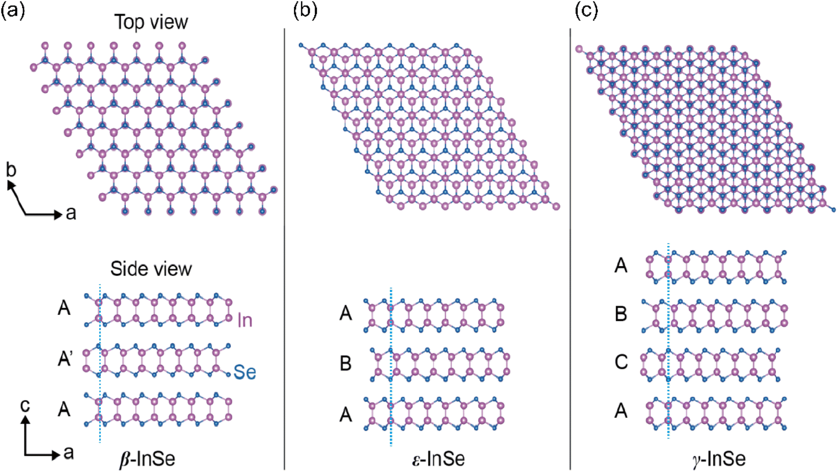 | ||
| Fig. 2 Three polytypes of InSe crystals. (a) β-InSe, (b) ε-InSe, (c) γ-InSe. | ||
Three basic polytypes with different crystal lattice structures and structural symmetries are summarized in Table 1. Usually, the physical properties of InSe strongly depend on its structural symmetry, thus, polytypes introduce large variations in the properties of the materials, particularly in optical properties. Unlike multilayer β-InSe nanosheets with inversion symmetry, γ-InSe and ε-InSe, which possess a hexagonal unit cell, exhibit broken inversion symmetry in all layer numbers, and have a strong second harmonic generation (SHG) effect.13 In addition, each space group allows selected vibrational modes, so Raman spectroscopy has been employed to characterize different polytypes with unique fingerprints. In both spectra, there are three main peaks, at about 115, 176 and 226 cm−1, which are common to all three InSe phases. There are additional characteristic peaks located at 197, 199 and 206 cm−1 that appear in the non-centrosymmetric structure of γ-InSe or ε-InSe.14
| Phase | Crystal system | Stacking sequence | Space point group | Lattice parameter (Å) |
|---|---|---|---|---|
| β-InSe | 2H (hexagonal system) | AA′AA′ | D 6h 4-P63/mmc (194) | a = 4.005, c = 16.96 |
| ε-InSe | 2H (hexagonal system) | ABAB |
D
3h
1-P![[6 with combining macron]](https://www.rsc.org/images/entities/char_0036_0304.gif) m2 (187) m2 (187) |
a = 4.005, c = 16.96 |
| γ-InSe | 3R (trigonal system) | ABCABC | C 3v 5-R3m (160) | a = 4.005, c = 25.44 (a = 26.83, α = 8.67°) |
Additionally, different phase structures also exhibit a variety of device characteristics. For instance, the robust piezo-phototronic effect, which is crucial for high-performance self-powered and flexible photodetectors, can be observed in ε- or γ-InSe but is absent in the β phase.15 Furthermore, ferroelectric switching effects are highly desired for in-memory computing and ferroelectric photovoltaics or detectors. β-InSe and γ-InSe, triggered by yttrium-doping (InSe:Y), show favorable in-plane and out-of-plane ferroelectric properties at room temperature, which are not observed in ε-InSe.16,17
The phase transition of 2D materials has received tremendous attention in recent years due to the attractive performance of multiphase materials and applications based on phase-change materials.18 Phase transition in InSe can be realized by pressure and thermal annealing. Su et al.19 demonstrated the phase transition of ε-InSe from a threefold symmetric pattern to a mirror symmetric pattern below 8.2 GPa pressure due to relative sliding between adjacent layers. Liu et al.20 and Cheng et al.21 demonstrated that γ-InSe transforms using the miniature diamond anvil cell. The phase structure transitions from rhombohedral semiconductor γ-InSe to the cubic phase with temperature at 2.3 K above 40 GPa and metallic phase above 11.4 GPa at room temperature, respectively. Phase transition under pressure is due to interlayer rotation, intralayer In–Se covalent bond variation, or adjacent layer sliding. In addition, under high temperature and high pressure (HTHP) conditions, Errandonea et al.22 observed the phase transition from the rhombohedral polytype to the monoclinic phase around 14.5 GPa and 420 K. Post-thermal annealing also affects the phase transformation of 2D InSe nanosheets. Osman et al.18 reported the phase transformation from β-InSe to γ-In2Se3 under thermal annealing at 200–400 °C. This transformation can be attributed to the diffusion of In into the Se lattice, causing the formation of γ-In2Se3. These studies of phase transition in InSe have extended its application in the field of phase-change materials.
2.2 Band structure and photoluminescence properties of two-dimensional InSe
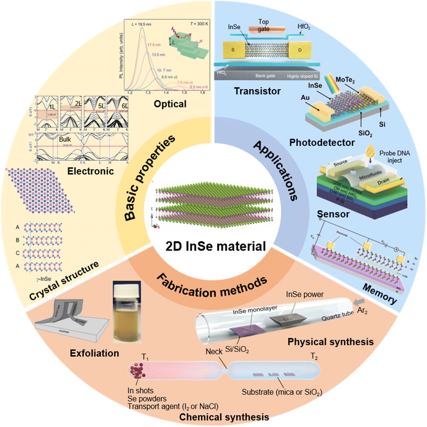
The photoelectric properties of semiconductor materials are intrinsically linked to their band structure. Recent advancements in both theoretical calculations and experimental methods have revealed more interesting photoelectrical properties of InSe. The band structure of InSe exhibits the characteristics of a regular change as a function of the thickness, similar to majority 2D semiconductor materials. Wasala et al. used first-principles calculations to study the electronic band structure of single-layer, multi-layer and bulk InSe crystals, as shown in Fig. 3(a).23 The valence band maximum (VBM) is located at the Γ–K direction in the InSe monolayer, forming a Mexican hat-shape, while the conduction band minimum (CBM) is at the Γ-point resulting in an indirect bandgap. Additionally, density functional theory (DFT) calculations revealed a transition from a direct to an indirect bandgap as the number of InSe layers decreases. Fig. 3(b) demonstrates that the band gap gradually widens as the number of two-dimensional InSe layers decreases. This trend is compatible with the pattern observed in the photoluminescence spectrum peaks for InSe materials of different thicknesses shown in Fig. 3(c).24 The few-layer InSe material possesses a direct band gap and exhibits strong free exciton recombination luminescence peak at room temperature in contrast to transition metal chalcogenides MX2 (M = Mo, W; X= S, Se, Te), which become direct bandgap materials only in the monolayer phase. Fig. 3(c) consolidates the statistical results for variations in the position of the photoluminescence peak for InSe flakes of different thicknesses and they are well consistent with the influence of quantum size confinement effects on the band gap of InSe. However, the near-infrared light emission under pressure using a diamond anvil cell revealed a different correlation. Fig. 3(d) demonstrates the pressure dependence of the optical band gap extracted from PL spectra. The band gap is strongly correlated with the number of layers (N = 5–30). As N > 20, the widening band gap results from the InSe lattice being compressed in all directions, and the intralayer compression at 1.5 GPa resulting in an emission blue shift of about ∼120 meV. In contrast, as N ≤ 15, the shrinking band gap is linearly correlated with pressure at the rate of 100 meV GPa−1.25 These findings facilitate the understanding of band gap and optical transition evolution in layered InSe. Building upon the inherent properties of two-dimensional InSe, the determination of InSe thickness can be achieved by identifying the photoluminescence peak position.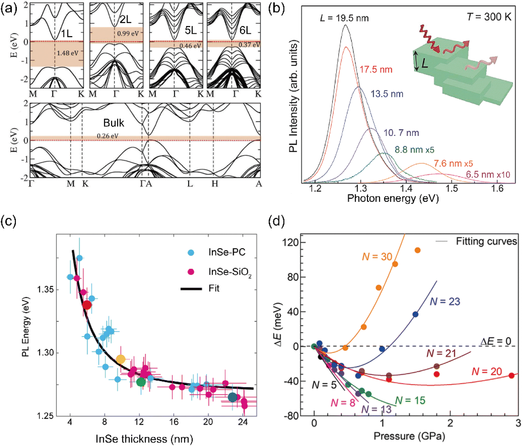 | ||
| Fig. 3 Thickness dependent band structure and photoluminescence properties of InSe materials. (a) Band structure of single-layer, few-layer (2, 5, 6) and bulk InSe materials. (b) Photoluminescence spectra of two-dimensional InSe materials with different thicknesses. Reproduced with permission.23 Copyright 2017, Royal Society of Chemistry. (c) Variation of peak position of InSe photoluminescence spectra with thickness. Reproduced with permission.24 Copyright 2020, Wiley-VCH. (d) P dependence of ΔE for InSe flakes with N = 5–30, ΔE < 0, the PL peak experiences a red shift, ΔE > 0, the PL peak experiences a red shift. Reproduced with permission.25 Copyright 2023, American Chemical Society. | ||
3 Two-dimensional InSe material fabrication and synthesis techniques
Within this section, we delve into the fabrication and synthesis techniques of 2D layered InSe semiconductors. These techniques for 2D layered materials can be broadly categorized into two main approaches: the top-down stripping method and the bottom-up direct synthesis method. The top-down stripping method involves isolating layered InSe nanoflakes by exfoliating the bulk single crystal leveraging the weaker interlayer van der Waals force along the c-axis direction. Nanoflakes detach from the bulk material through the application of mechanical force or shear force. The notable techniques in this approach are mechanical exfoliation (ME) and liquid phase exfoliation (LPE). Conversely, the bottom-up direct synthesis method can be divided into chemical synthesis methods and physical synthesis methods. Layered InSe nanoflakes are prepared through chemical reaction either in the vapor phase or liquid phase and physical phase deposition.3.1 Top-down method
Mechanical exfoliation or micromechanical cleavage has emerged as the predominant method for the preparation of 2D materials since the first monolayer graphene was obtained by mechanical exfoliation using Scotch tape.26 This method has proven to be an effective way for most 2D materials, including transition metal dichalcogenides (TMDs), hexagonal nitride boron (h-BN), and BP.27–29 As shown in Fig. 4(a), the mechanism of mechanical exfoliation involves applying Scotch tape on the surface of a bulk crystal with the help of adhesive tape and exerting a normal force to repetitively peel off nanoflakes until they are obtained.29,30 However, obtaining high-quality InSe nanoflakes through mechanical exfoliation requires to start from a bulk single crystal. Currently, several techniques such as the Bridgman method, the traveling heater method, the zone melting method and the horizontal gradient freeze are capable of producing high-quality bulk single crystals.31–34 Mechanical exfoliation has the advantage of producing high-quality 2D layers that inherit the bulk crystal's excellent crystal quality. As a result, this method is generally used to fabricate 2D InSe nanoflakes for fundamental research, exploring novel physical phenomenon and demonstrating novel functional devices.35 For instance, Venanzi et al. investigated the photoluminescence (PL) in InSe and its dependence on thickness and temperature.36 Meanwhile, Bandurin et al. found that the carrier mobilities in mechanically exfoliated 2D InSe field effect transistors exceed 103 cm2 V−1 s−1 at room temperature and 104 cm2 V−1 s−1 at liquid-helium temperature.37 | ||
| Fig. 4 Morphological, size and structural characterization of InSe flakes. (a) Schematic illustration of the mechanical exfoliation process. Reproduced with permission.29 Copyright 2018, Elsevier. (b) AFM image of a multi-terraced InSe flake exfoliated onto a SiO2/Si substrate. (c) Thickness profile measured along the ABCD path indicated in (b). Horizontal dashed lines indicate the thickness expected by the sequential stacking of InSe single layers. Reproduced with permission.44 Copyright 2015, Elsevier. (d) Representative TEM image of an isolated exfoliation-InSe flake. (Inset): Schematics of the LPE process: sonication; ultracentrifugation; and stable dispersion of exfoliated β-InSe flakes, respectively. (e) Lateral size and thickness statistical analyses for exfoliation InSe flake dispersion. (Inset): Statistical analysis for exfoliation-InSe surface area. (f) Raman spectra for c-InSe (cyan trace) and exfoliation-InSe (orange trace) samples. (Inset): Schematic of atomic vibrations for β-InSe Raman active modes. Reproduced with permission.40 Copyright 2018, Wiley-VCH. (g) Low-resolution TEM image of a representative InSe flake along with a magnified high-resolution TEM image (Inset). (h) and (i) XPS analysis of the InSe flakes. Reproduced with permission.43 Copyright 2018, Wiley-VCH. | ||
Although 2D InSe nanosheets from mechanical exfoliation have been promising for fundamental research and novel device fabrication, mechanical exfoliation falls short in producing large-scale nanosheets with regulated thickness and efficient production. Identifying these limitations, liquid phase exfoliation has been proposed as a convenient, low cost and high yield method for fabricating large amounts of 2D materials due to its advantages over mechanical exfoliation, which is also suitable for printed electronic device applications.38 There are three liquid phase exfoliation mechanisms including sonication-assisted exfoliation, ion intercalation and ion exchange.39 During the liquid phase exfoliation of 2D layered InSe, a variety of solvents such as 2-propanol (IPA),40N-methyl-2-pyrrolidone (NMP)41 and ethanol42,43 have been utilized with the help of an external force like ultrasonication, milling and shear mixing. Petroni et al. employed IPA solvent to produce single and few-layered InSe flakes.40 The authors started from β-InSe single crystals, which were pulverized in a mortar and then ultrasonicated in IPA for six hours at a temperature range of 25–35 °C. The obtained dispersion was ultracentrifuged at different speeds of 1000 rpm, 2500 rpm or 5000 rpm for 30 min at 15 °C to adjust the morphology, lateral size and thickness of the InSe flakes. Statistical analyses revealed that the prepared InSe flakes had maximum lateral sizes ranging from 30 nm to a few micrometers with the thickness ranging from 1 to 20 nm, however, most InSe flakes had thickness around ∼5 nm as shown in Fig. 4(e). Conversely, Li et al. employed NMP for extensive InSe nanosheets via the liquid exfoliation technique.41 Bulk InSe crystals and NMP solution were firstly milled for 30 minutes and ultrasonicated for six hours at a power of 300 W in an environment below 20 °C. The suspension liquid was then centrifuged at a speed of 2000 rpm for three minutes and dried in a vacuum oven at 80 °C for two hours to remove the residual solution. Finally, the supernatant was centrifuged at the speed of 18![[thin space (1/6-em)]](https://www.rsc.org/images/entities/char_2009.gif) 000 rpm for 10 minutes. The end product mostly consisted of InSe nanosheets with seven to eight layers in thickness. However, traditional liquid phase exfoliation methods, especially those using surfactant-assisted aqueous dispersions or organic solvents with high boiling points, can compromise electronic properties due to residual surface contamination and chemical degradation. Hence, Kang et al. utilized a binary, low-boiling point ethanol–water cosolvent system, ensuring minimal processing residues during their exfoliation process.43 They exfoliated InSe crystals in ethanol–water mixtures with different volume ratios and subsequently centrifuged them to remove remaining aggregates as shown in Fig. 4(g–i). Their findings revealed that a 3:2 ethanol to water volume ratio was optimal for producing an InSe flake dispersion with the highest concentration, demonstrating remarkable stability and minimal oxidation.
000 rpm for 10 minutes. The end product mostly consisted of InSe nanosheets with seven to eight layers in thickness. However, traditional liquid phase exfoliation methods, especially those using surfactant-assisted aqueous dispersions or organic solvents with high boiling points, can compromise electronic properties due to residual surface contamination and chemical degradation. Hence, Kang et al. utilized a binary, low-boiling point ethanol–water cosolvent system, ensuring minimal processing residues during their exfoliation process.43 They exfoliated InSe crystals in ethanol–water mixtures with different volume ratios and subsequently centrifuged them to remove remaining aggregates as shown in Fig. 4(g–i). Their findings revealed that a 3:2 ethanol to water volume ratio was optimal for producing an InSe flake dispersion with the highest concentration, demonstrating remarkable stability and minimal oxidation.
Mechanical exfoliation and liquid phase exfoliation methods have found extensive application in InSe fundamental research. However, there are issues with the uncontrollably small size and thickness of 2D stacked nanoflakes when they are prepared. Additionally, the liquid phase exfoliation method inevitably results in defects and unintentional doping of the semiconductor.
3.2 Bottom-up method
In the quest to fabricate large-area two-dimensional material films, researchers have pivoted towards bottom-up methods as they address numerous challenges intrinsic to the exfoliation method. Bottom-up strategies encompass both chemical synthesis and physical synthesis approaches, both of which have been extensively explored for the fabrication of 2D materials. Scalable growth of high-quality 2D materials is critical for their utilization in technological applications. Remarkably, bottom-up methods can produce 2D materials with large areas and controllable thicknesses, which is of great significance for the imminent integration of 2D materials into electronic and optoelectronic devices.Chemical Vapor Deposition (CVD) has emerged as a predominant bottom-up technique for the preparation of 2D layered materials. This intricate process mainly involves vapor phase components, precursor absorption, nucleation and transport. The choice of precursor, growth mode and appropriate substrates hold paramount importance in the production of 2D materials, a wide variety of morphologies are obtained under different growth conditions.45,46 Huang et al.47 proposed a novel phase-engineered route to synthesize ultrathin single-crystalline InSe nanoflakes in a stable CVD system with mass-transfer and space-confinement. As shown in Fig. 5(a), a suitable precursor of low melting point InI powder was used as the indium source and Se powder as the selenium precursor. The metastable valence state of Se under a reductive H2 atmosphere is advantageous for the phase control growth of InSe nanoflakes. Notably, the utilization of a space-confined CVD method enabled the selenization of the InI precursor via Se powder, leading to the fabrication of ultrathin InSe flakes within a microreactor containing two-stacked mica substrates. The study further revealed that when the H2 content was high and the Se content was low, InSe was produced rather than In2Se3. The spacing between the two substrates could be effectively controlled to create a stable local atmosphere for 2D InSe growth, ensuring stable mass transfer to maintain accurate reactant concentrations and controllable feed rates. The size and thickness, as well as the grain orientation, could be precisely controlled in the space-confined CVD system by changing the spacing. While this approach yielded single crystalline InSe with high crystallization quality, the lateral size of InSe nanoflakes ranged from 10 to 60 μm, which is slightly below practical application requirements. Chang et al.,48 reported a distinct CVD method for synthesizing large-area InSe atomic layers through the vapor phase reaction of In2O3 with Se. The processing involved the use of argon and hydrogen as carrier gases and reductant. The InSe monolayers were in the shape of a triangle with a lateral size of about tens of micrometers, and the largest ones reached up to 250 μm on substrates farthest from the In2O3 precursor, while the rarely distributed flakes indicated low density nucleation. This study revealed the dependence of nucleation density on the growth position in CVD, with a closer growth position leading to a higher nucleation density. This observation paved a way for the centimeter-scale monolayer InSe films to be integrated into devices. Additionally, a catalyst-free CVD was also used to fabricate 2D InSe. Wu et al.49 recently employed this approach to create InSe nanobelts. High-purity InSe powder was loaded into an alumina boat and then placed in the center of the heating zone. A pre-cleaned SiO2/Si substrate was placed at the downstream position approximately 17 cm away from the powder source. The chamber was filled with Ar at a pressure of about 56 Pa. Subsequently, the source was heated to 850 °C and kept at this temperature for 35 minutes. After the furnace cooled naturally to the room temperature, InSe nanobelts were formed on the substrate. As the thickness of InSe nanobelts decreased from 562 to 165 nm, a blue shift in the photoresponse peak was observed, indicating potential applications in spectral engineering for full-color imaging. Recently, Song et al.50 reported a successful approach for growing a polymorph-selective, high-quality 2D InSe by metal–organic chemical vapor deposition (MOCVD). Using trimethylindium (TMIn; (CH3)3In) and dimethyl selenide (DMSe; (CH3)2Se) as the In and Se sources, phase-pure InSe was achieved by a flow modulation technique. InSe nucleation occurs on the substrate in a Se-deficient environment, with lateral growth of InSe at low temperatures (350–500 °C). As shown in Fig. 5(b), the crystalline thin films grow on c-plane sapphire with high quality and are highly stoichiometric on 2-inch wafers, with thickness adjusted by growth time. In general, there are a series of parameters, such as the precursors, substrates, gas flow rate, gas atmosphere, temperature, location of precursors/substrates and heating duration, which play a critical role in the orientation morphology, composition, thickness, and crystalline quality of products. Meanwhile, asynchronous sublimation of precursors may lead to inhomogeneous elemental distribution and even phase segregation of the products, thus, causing deviation from the intended atomic molar ratio.
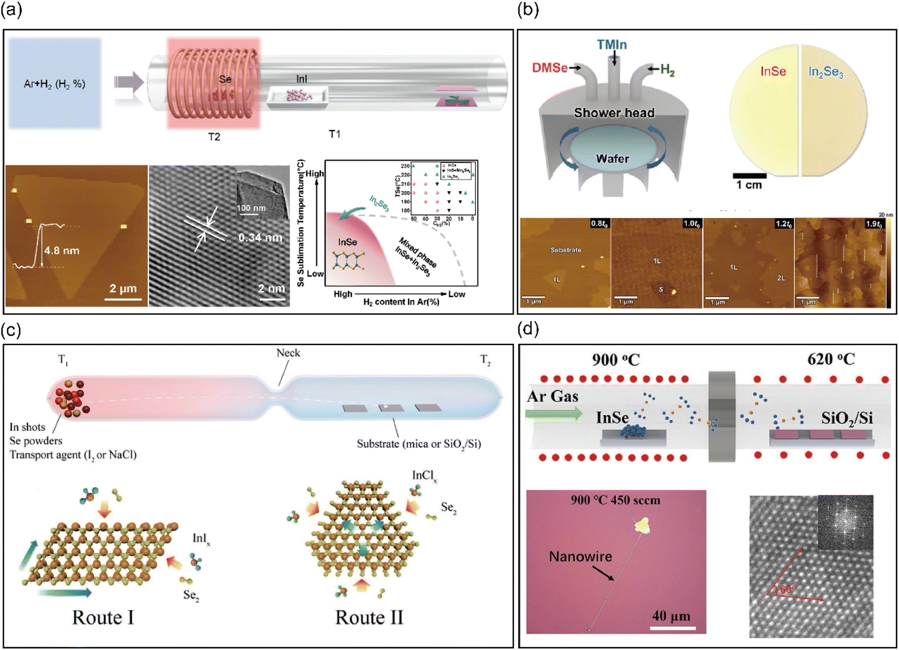 | ||
| Fig. 5 Chemical synthesis methods of 2D layered InSe nanoflakes. (a) Schematic diagram of 2D InSe nanoflake growth by a space-confined CVD system within the micro-reactor constructed from two stacked mica substrates, optical image and TEM characterization of InSe flakes. Reproduced with permission.47 Copyright 2018, Wiley-VCH. (b) Schematic diagram of the experimental setup for MOCVD synthesis of InSe and AFM image of the InSe thin film, where t0 denotes the time for growing a fully stitched monolayer of InSe on sapphire. Reproduced with permission.50 Copyright 2023, Elsevier Inc. (c) Schematic diagram for the synthesis of InSe nanoflakes via the controlled CVT method in different routes. Reproduced with permission.54 Copyright 2019, Wiley-VCH. (d) Schematic diagram of InSe flakes and nanowires via homoepitaxial growth on SiO2/Si substrates and image of InSe flakes. Reproduced with permission.66 Copyright 2020, Wiley-VCH. | ||
Traditionally, CVT has proven to be a reliable process for fabricating high-quality bulk crystals. It represents a category of reactions in which source materials are generally evaporated or sublimated from the high temperature region and eventually crystallize at the low temperature region via a sublimation–transport–solidification process.51,52 Recently, it was found that CVT can synthesise 2D materials directly by introducing suitable substrates and slow growth rates.53 Yuan et al. proposed a controlled, one-step chemical vapor transport method for the synthesis of 2D InSe nanoflakes.54 As shown in Fig. 5(c), In shots and Se powder were used as precursors and placed in an ampoule with a neck. I2 or NaCl served as both the transport agent and the halogen source simultaneously. Mica or SiO2 substrates were placed at the other end of the ampoule to facilitate deposition and growth of InSe. There are two routes for InSe crystal growth. Route I involved the formation of InIx (using I2 as the transport agent) and selenium as the intermediate transport species, where InSe nanoflakes grew mainly along two crystallographic directions to produce a rhombohedral shape on mica and SiO2 substrates. Route II involved the epitaxial synthesis of triangular/hexagonal shapes on mica from gaseous InClx (using NaCl as a transport agent) and selenium, with the nanoflake growing along one crystallographic direction. Significantly, the non-epitaxial grown free-standing InSe nanosheets via route I could be randomly distributed on an arbitrary substrate. The aspiration to directly grow 2D InSe was achieved by reducing the amount of source materials and transport agent while increasing the temperature gradient between the reaction and deposition area. However, a trade-off emerges, the augmented precision is at the expense of significantly suppressed growth rate, thus CVT requires an extremely long growth period.
In contrast with CVD and CVT methods, molecular beam epitaxy (MBE) stands out as a sophisticated vapor deposition technique conducted in an ultra-high vacuum environment making use of substrates and/or epilayers characterized by van der Waals surfaces without dangling bonds. MBE provides a promising approach for fabricating high-quality, large-scale, and high uniformity 2D materials, as well as fabricating multilayer heterostructures with abrupt interfaces.55–57 In the MBE process, the epitaxial layer grows upon a single-crystalline substrate, such as 2D substrates or three-dimensional substrates without dangling bonds.55,57,58
Recently, various single crystalline substrates including GaAs(001),59 graphene,60–62 Si(111),63c-plane Al2O3 substrates64 and sapphire65 have been employed in the MBE synthesis of 2D InSe. Specifically, Poh et al.60 and Zhang et al.62 proposed an MBE method wherein they utilized In2Se3 and Se powders as precursor materials and adopted graphene-covered SiO2/Si or 6H–SiC(0001) as the substrate. Upon exposing the In2Se3 precursor to a Se-deficient atmosphere, decomposition led to InSe being deposited onto the graphene substrate. Subsequently, In2Se3 can be obtained when the 2D InSe is exposed to an environment containing sufficient Se at high temperature. While MBE-fabricated 2D InSe nanosheets exhibited higher quality, their lateral size was restricted, only spanning several hundred nanometers. Hao et al.66 unveiled a catalysis-free approach to synthesize elongated and straight InSe nanowires through edge-homoepitaxial growth. As shown in Fig. 5(d), triangular 2D InSe nanosheets were initially prepared on SiO2/Si substrates by using InSe powder as the reactant precursor and evaporation by heating at a high temperature (800 °C). When the temperature was increased to 900 °C, partial decomposition of the InSe vapor molecules into selenium droplets occurred. Subsequently, the InSe species dissolved in supersaturated eutectic Se droplets and were adsorbed on the edges of existing InSe nanosheets. With the action of optimal lattice alignment and reduced binding energy, InSe nanowires proliferated from the nanosheet edges via edge-homoepitaxial growth. Liu et al.63 reported a strategic approach to map out the growth window as functions of the Se/In ratio and temperature for γ-InSe on the Si (111) substrate in MBE. Large S-scale InSe films were grown on a 3-in. Si (111) substrate in varying temperature and flux ratios, and the mechanism of the spiral growth mode and layered growth mode is revealed. A pure phase of γ-InSe could be obtained at varying Se/In flux ratios at temperatures around 375 °C, at Se/In flux ratios between 3 and 3.75 at 337.5 °C, and at Se/In flux ratios from 2 to 2.75 at 300 °C. This study provided a guidance system for single-phase InSe growth. Recently, Claro et al.65 presented the epitaxial growth of an InSe/GaSe heterostructure on sapphire and Si substrates. Highly oriented GaSe can be obtained on Si (111) substrates, and single-phase InSe was grown on the top of the GaSe buffer layer. This work presents a breakthrough in the controlled epitaxial growth of functional heterostructures and proves the feasibility of combining it with Si technology.
While the MBE fabrication of 2D materials benefits from reduced lattice-matching constraints and achieves a dangling-bond-free surface, its prolonged growth duration coupled with the need for an ultrahigh vacuum environment, which brings exorbitant costs, is a disadvantage hindering its widespread industrial application.
The ALD method, a novel growth technique, has been increasingly recognized for its role in the advancement of 2D materials, showcasing tremendous potential in recent innovations.67 The ALD method has a unique growth mechanism and distinguished capabilities for achieving atomically precise controllability over the growth of 2D materials. Notably, it is performed at low temperatures and enables nanoscale films with excellent uniformity and controllable thickness.68,69 The high quality of the ALD film materials results from the relatively slow growth rate.70 During the ALD process, thin films evolve from surface self-saturated reactions of the precursor, the thin film can be effectively controlled at the atomic level and exhibits excellent morphological control due to the layer-by-layer reaction manner of ALD growth, and monolayers with excellent large-area uniformity can be achieved.35,69,71 Crucially, selection of the precursor and substrate plays a pivotal role in the ALD process because ALD is fundamentally a surface-controlled procedure where the self-limiting reactions occur on substrate surfaces.67 Recently, Browning et al.72 successfully employed the ALD technique to achieve large-area 2D InSe thin film deposition at low temperatures. In this work, SiO2/Si, plain glass and fluorinated tin oxide (FTO) coated glass slides were used as substrates. InCl3 and H2Se were used as the In and Se precursors, respectively, with nitrogen as the carrier gas. They managed to grow InSe thin films at 350 °C on either SiO2/Si or FTO substrates. Impressively, the ALD-grown γ-InSe thin films on SiO2/Si substrates displayed commendable crystalline and optical characteristics, which were comparable in composition to those prepared by other methods. In spite of numerous advantages, ALD suffers from relatively high manufacturing cost as compared to CVD and CVT owing to the use of expensive precursors and lower growth rate.
In addition, chemical solution synthesis offers an alternative approach utilizing the chemical reactions in solution to synthesize 2D materials at much lower temperatures than CVD and CVT methods. Chemical solution synthesis exhibits numerous advantages, including low cost, high yield, and universal compatibility with diverse substrates. It was originally developed for the fabrication of noble metal nanoparticles and various nanostructured materials. Chemical solution synthesis has evolved as an influential means for 2D materials; the ideal solution routes should be scalable, produce high yields, and allow phase control, this ensures the formation of 2D materials with controlled morphology and thickness.73,74 The size and shape of the products can be fine-tuned via the temperature, reaction time, and molar ratio of the precursors. Illustratively, Ning et al.74 proposed a straightforward method to yield InS nanocrystals in chemical solution with a lateral size in the range of 10–50 nm. During the synthesis of zinc blende InSe (ZB–InSe) nanocrystals, InCl3 and oleylamine (OLA) were placed into a three-neck flask and heated to remove water. Then selenourea/OLA solution (0.1 mmol mL−1) was injected with a syringe. The temperature of the solution was maintained at 260 °C in 10 minutes to grow InSe nanocrystals, then the solution was quenched to room temperature with toluene. InSe nanocrystals can be obtained by centrifugation with the assistance of methanol. The reaction temperature and molar ratio of precursors have little effect on the shape and size of ZB–InSe. When the reaction temperature is higher than 330 °C, ZB–InSe transform into the hexagonal crystal structure In2Se3 (H–In2Se3). Subsequently, Airo et al.75 synthesized rhombohedral InSe nanocrystals by refluxing InCl3 and Se in oleylamine (OLA) in a pot at a temperature of 200 °C with a molar ratio of 1:1. OLA is used to reduce the selenium concentrations while acting as both a solvent and capping agent in this method. The size of as-synthesized InSe nanosheets decreases with increasing reaction time, the nanosheets broken with a longer reaction time, resulting in a small size distribution of mainly 8 nm obtained in 60 minutes. Furthermore, Lauth et al.76 presented another solution-processable method for ultrathin 2D InSe nanosheets with lateral size up to 800 nm. In this method, a lamellar ligand template is prepared from octadecylamine (ODA) with InCl3 preceding the growth of ultrathin InSe layers, and then selenourea (dissolved/suspended in ODE) is introduced into the reaction. InSe nanosheets can be obtained at 240 °C with an average thickness of 5 nm and lateral sizes ranging from 350 to 800 nm, which strongly depends on the reaction time. Recently, Karmakar et al.77 reported a molecular precursor mediated selective synthesis method for phase-pure cubic InSe with fewer defects. A single source molecular precursor, tris(4,6-dimethyl-2-pyrimidylselenolato) indium(III), provided better control over the stoichiometry and phase purity. This synthesis route provided scientific evidence for 2D InSe fabrication. In general, the processing parameters such as temperature, chemical reagents, concentrations and reaction time can be modified to adjust the shape, size, and uniformity of the solution-grown nanostructures. Given their versatility, materials synthesized via chemical solution hold immense promise for industrial applications, especially in contexts demanding large-scale synthesis.73,78
Vacuum evaporation is one of the initial methods of physical vapor deposition used for the synthesis of large-scale atomically thin InSe nanoflakes on Si/SiO2 substrates.79 This method involves the evaporation of source materials and deposition on a substance or substrate without chemical reaction, resulting in high quality 2D nanosheets or thin film. Zhou et al.79 adopted vacuum evaporation to synthesize high-quality and large-area monolayer InSe on the SiO2/Si substrates. As shown in Fig. 6(a), InSe powder served as the evaporation source and was heated to 830 °C, the SiO2/Si substrate was placed approximately 10–15 cm away from the evaporation source. 2D InSe nanosheets of various sizes and layers could be obtained by changing the growth time. Remarkably, monolayer InSe was obtained within 10 minutes, whereas multilayer InSe demanded extended deposition time. Based on this method, Balakrishnan et al.80 introduced an epitaxial growth strategy tailored for large area γ-InSe crystals. This was achieved using a physical vapor transport furnace on ε-GaSe substrates with a low density of dangling bonds. As shown in Fig. 6(b), by exploiting the temperature gradient within the tube furnace, large-area (>103 μm2) InxSey layers were acquired with controlled stoichiometry and phase variations in InxSey compounds including γ-InSe as well as α, β, γ phases of In2Se3. The variation occurred depending on the position of the substrate from lower temperature to higher temperature.
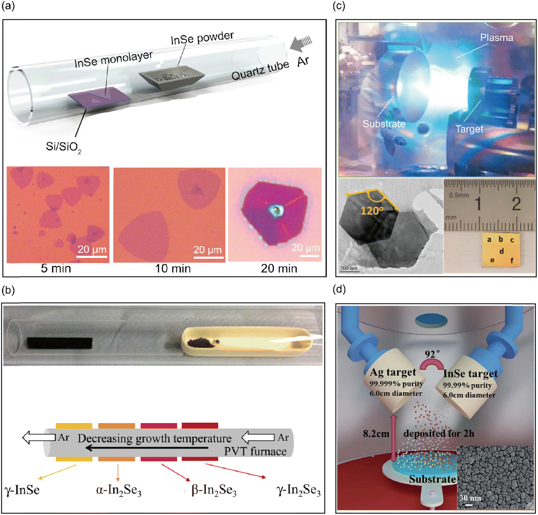 | ||
| Fig. 6 Physical synthesis methods of 2D layered InSe nanosheets. (a) PVD setup and optical images of atomically layered InSe. Reproduced with permission.79 Copyright 2019, IOP. (b) Image and schematic diagram of the quartz tube for the PVT growth of InxSey on ε-GaSe. Reproduced with permission.80 Copyright 2018, IOP. (c) Image of the laser ablation process, low-resolution TEM image and optical image of InSe nanosheets and structure. Reproduced with permission.81 Copyright 2017, American Chemical Society. (d) Illustration of direct current-radio frequency sputtering system setups and SEM micrographs of Ag doped InSe nanofilm. Reproduced with permission.88 Copyright 2020, Royal Society of Chemistry. | ||
In addition, Yang et al.81 reported the direct growth of wafer-scale layered InSe nanosheets using the PLD method. PLD is a typical bottom-up physical method widely used for the deposition of 2D layered materials and complex compound thin films.82–84 As shown in Fig. 6(c), layered InSe films were deposited on SiO2 (300 nm)/Si substrates in a high vacuum chamber with a pressure of 1.5 × 10⁻⁷ Torr. The bulk InSe target was placed 4 cm away from the substrate, which was heated to 600 °C accompanied by energetic laser pulses hitting the surface of the polycrystalline InSe target, which vaporized a large number of atoms, ions, molecules, and clusters that reassembled into a film on the preheated substrate. Both the InSe target and substrates were rotated during the deposition process to ensure uniformity and high crystallinity with macrotexture features, and stoichiometric growth that could be precisely controlled in situ. According to the formation kinetics of the 2D-layered InSe crystals, the formation was found to proceed via two sequential phase transformations, the exothermic reorganization of the amorphous phase and the exothermic formation of the crystalline phase.85 The thickness of the thin film can be directly adjusted by changing the number of laser pulses, which allows precise control of the InSe layer number. The lower growth temperature and controllable thickness makes PLD much more advantageous, but PLD suffers from relatively high production cost owing to a high-vacuum environment.
Moreover, sputtering is a standard industrial fabrication technique, esteemed for its repeatability and large area deposition of high quality crystalline films with fair uniformity and thickness.86,87 As shown in Fig. 6(d), Yan et al.88 fabricated pure InSe and Ag-doped InSe nanofilms utilizing a direct current-radio frequency sputtering method. A smooth and uniform Ag-doped InSe nanofilm, devoid of cracks and spanning an average size of 30–40 nm, was successfully realized by precise regulation of the sputtering process parameters (such as sputtering temperature, reactant pressure, radio frequency power, deposition time, and gas flow). Although the products via sputtering exhibit a pristine InSe phase, the resultant InSe is predominantly polycrystalline. Moreover, the surface morphology of the grown InSe is relatively rough as compared to that of the CVD grown and PVD grown samples.
Fundamentally, CVD, MBE, PVD, and PLD have proven to be promising techniques for preparing 2D layered materials with unique advantages, Nevertheless, prior to envisioning their tangible industrial integration, there are still challenges to be addressed. For example, these encompass hurdles like pursuit of large-scale production, exacting thickness accuracy, and the assurance of high crystal quality. To streamline the understanding, a concise summary encapsulating the advantages and disadvantages of these synthesis techniques is captured in Table 2.
| Fabrication method | Thickness (nm) | Lateral size | Advantage | Disadvantage | Ref. |
|---|---|---|---|---|---|
| ME | Monolayers to bulk | Up to tens of micrometers | High crystalline quality inherited from the bulk | Low yield | 37 and 89 |
| Easy handling and low cost | Random distribution of flake size and thickness | ||||
| Not scalable | |||||
| LPE | Few layers | Up to tens of micrometers | High yield | Low crystalline quality | 40–43 |
| Better control on size | Small size | ||||
| Low cost | |||||
| CVD | Monolayers to few layers | Up to centimeter scale | High-quality layers | Expensive equipment | 47, 48 and 90 |
| Precise control over thickness | Stringent synthetic conditions | ||||
| Highly reproducible | Limited to few substrates | ||||
| High scale uniformity | |||||
| CVT | Monolayers to few layers | Up to centimeter scale | High-quality layers | Expensive equipment | 54 |
| Precise control over thickness | Stringent synthetic conditions | ||||
| Highly reproducible | Limited to few substrates | ||||
| High scale uniformity | Low growth rate | ||||
| MBE | Monolayers to few layers | Up to tens of micrometers | Well-oriented flakes | Process hard to control | 59–63 |
| Precise control over thickness | Expensive equipment | ||||
| No catalyst | Needs appropriate substrates | ||||
| ALD | Monolayers to few layers | Up to few micrometers | Well-oriented flakes | Expensive equipment | 72 |
| Precise control over thickness | Low growth rate | ||||
| Low temperature | |||||
| Chemical solution synthesis | Monolayers to few layers | Up to hundreds of nanometers | High yield | Nano-scale size | 74–76 |
| Low cost | Low crystalline quality | ||||
| High universality of the substrate | |||||
| VE | Monolayers to few layers | Up to few micrometers | Large sized flakes | Expensive equipment | 79 |
| High scale uniformity | Process hard to control | ||||
| Higher phase purity | High growth temperature | ||||
| PLD | Monolayers to few layers | Up to millimeters | Large sized flakes | Expensive equipment | 81 and 91 |
| High scale uniformity | Process hard to control | ||||
| Higher phase purity | |||||
| Sputtering | Monolayers to few layers | Up to tens of nanometers | Precise control over thickness | Low crystalline quality | 88 |
| High scale uniformity | Nano-scale size | ||||
| Higher phase purity |
4 InSe advanced device application
Two-dimensional materials present significant potential for the development of high-performance FETs due to their dangling-bond-free surface and inherent nanoscale thickness. Their exceptional electronic, optical, and mechanical characteristics make them excellent candidates for the next-generation electronic and optoelectronic devices. Within the large library of two-dimensional semiconductor materials, encompassing transition metal chalcogenides, metal chalcogenides (MCs) and black phosphorus, the comparison of the optoelectronic properties of different 2D semiconductor materials is shown in Table 3. Carrier mobility is a crucial parameter in semiconductor materials, defined by the classical Drube formula of μ = eτ/m*, where e is the electron charge, τ is the average value of the momentum relaxation time, and m* is the effective mass.92 In a comparison of multilayer InSe based transistors with other state-of-the-art III–V materials based transistors, InSe stands out for field-effect transistor (FET) applications due to its extremely lower electron effective mass (me = 0.143 m0) compared to MoS2 (m* = 0.45 m0) and WS2 (m* = 0.34 m0). This lower effective mass of InSe contributes to higher electron mobility, enhancing transport characteristics across a wide range of InSe thicknesses.93,94 Furthermore, being a direct bandgap semiconductor with small enough bandgap energy with fewer layers (>6 nm), InSe is also capable of converting photoelectric signals in a wide spectral range of UV-visible-infrared spectrum. In response, the research community has poured substantial effort into a systematic exploration and optimization of InSe device performance. Many strategies including dielectric engineering, modification of channel material, optimization of metal contact and encapsulation have been wielded effectively to either improve the performance or diversify the functionalities of both electronic and optoelectronic devices, notably high-mobility field-effect transistors and photodetectors.37,89,90,95,96| Material | E g (direct) (eV) | E g (indirect) (eV) | m* (m0) | Intrinsic doping | μ FE (cm2 V−1 s−1) | On/off ratio | Spectral response | Ref. | |
|---|---|---|---|---|---|---|---|---|---|
| a Abbreviations: NIR, near-infrared; VIS, visible; m0: the free electron mass. | |||||||||
| InSe | 1.26–1.42 (>6 nm) | 2.0 (<7 L) | 0.143 | n | 1055 | 108 | VIS to NIR | 90, 97 and 98 | |
| BP | 0.3 (bulk) 2.0 (1 L) | — | 0.14 (e) 0.18 (h) | Ambipolar | 984 | 105 | Mid-IR | 99–101 | |
| MoS2 | 1.89 (1 L) | 1.23 (bulk) | 0.45 | n | 200 | 108 | VIS | 94, 102 and 103 | |
| MoSe2 | 1.55 (1 L) | 1.09 (bulk) | 0.53 (e) 0.65 (h) | n | 50 | 106 | VIS to NIR | 104–107 | |
| WSe2 | 1.66 (1 L) | 1.21 (bulk) | 0.31 | Ambipolar | 250 | 106 | VIS | 108–112 | |
| WS2 | 2.01 (1 L) | 1.35 (bulk) | 0.33 | n | 50 | 106 | VIS | 113–115 | |
4.1 InSe field effect transistor
Based on first principles theoretical calculations combined with high field intensity magnetic spectrum experimental results, Garry W. Mudd et al.97 highlighted the prospective application of InSe in high mobility electronic devices. However, early renditions of InSe FETs fabricated with a multilayer InSe channel and a Si substrate coated with a SiO2 layer as a dielectric exhibited lower than expected field effect mobility.91,116,117 This low mobility could be attributed to various extrinsic scattering sources, such as charge impurities at the interface, as well as intrinsic defects within the 2D materials like charged impurities, remote phonons, atomic vacancies, and structural dislocations. Predominantly, in 2D materials the dielectric surface and the dielectric/semiconductor interface are dominant sources of carrier scattering.90,105,117–119 Conventional dielectric substrates such as SiO2, Al2O3, and HfO2 inherently possess hydrophilic properties, which are associated with a large number of hydroxyl groups and other charge trap absorbers.90 Moreover, the complete exposure of the ultrathin channel materials to the external environment exacerbates carrier scattering, leading to reduced field-effect mobility.105,120 Therefore, scientists have looked towards dielectric interfacial engineering, which provides promising ways to achieve high carrier mobilities in 2D channels. Feng et al.90 were the pioneers of this strategy, introducing a polymethylmethacrylate (PMMA)/SiO2 bilayer dielectric as the bottom dielectric for back-gate InSe FETs (Fig. 7(a)). The mobility of multilayer InSe FETs fabricated on a PMMA/SiO2 bilayer dielectric showcased impressive mobility, registering a 94.5-fold increase compared to the SiO2 dielectric layer. Moreover, devices constructed with a PMMA/Al2O3 bilayer dielectric exhibited a high field-effect mobility of 1055 cm2 V−1 s−1 (Fig. 7(b)). The improvement of field-effect mobility with the PMMA/Al2O3 bilayer dielectric is mainly attributed to the substantial reduction in interfacial Coulomb impurities or surface polar phonon scattering since PMMA is a defect-free polymer. Based on this method, Zhang et al.121 implemented a hybrid dielectric strategy to improve the performance of InSe FETs. The FETs integrated with a hybrid dielectric layer consisting of 200 nm PMMA and HZO/AlO (HfO2/ZrO2/Al2O3) recorded high carrier mobility (∼863 cm2 V−1 s−1). In a similar vein, Jiang et al.118 fabricated a bottom-gate staggered InSe FETs with a PMMA/HfO2 bilayer gate dielectric and a PMMA back-channel encapsulation. This architecture not only delivered exceptional mobility (∼1200 cm2 V−1 s−1) under ambient conditions but also showed high stability and mobility, thanks to the PMMA back-channel encapsulation that protected the InSe FETs from the deleterious influence of water and oxygen molecules.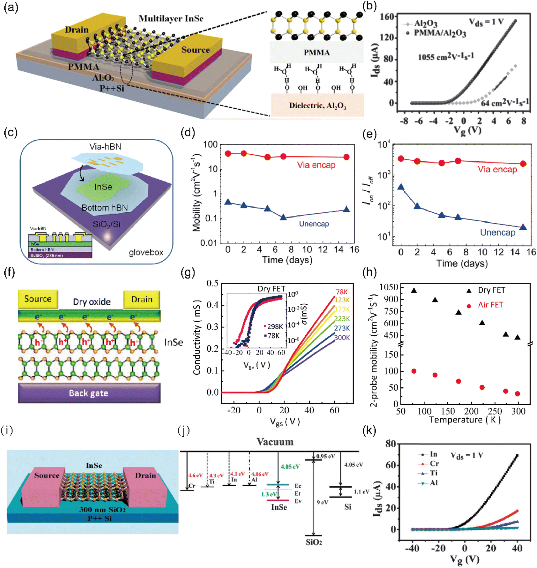 | ||
| Fig. 7 InSe-based field-effect transistor with different optimization strategies. (a) Schematic of back-gate multilayer InSe FETs consisting of a PMMA/Al2O3 back gate insulator and Au/Cr electrodes (40/20 nm). (b) Transfer characteristics of a multilayer InSe transistor with a polymer-assisted (200 nm/50 nm) PMMA/Al2O3 dielectric. Reproduced with permission.90 Copyright 2014, Wiley-VCH. (c) Schematic of the InSe-via device when the via-contact h-BN covers InSe in a glovebox to encapsulate it and to form an electrical connection. (d) Mobility and (e) on/off ratio with time for both device configurations. Reproduced with permission.127 Copyright 2014, American Chemical Society. (f) Schematic illustration of a back-gate InSe FET covered with a dry oxide. (g) Transfer characteristics with forward and backward scans of the gate voltage, comparing the hysteretic effect for the dry FETs. (h) Temperature-dependent mobilities of InSe FETs with air or dry oxides covered on top. Reproduced with permission.128 Copyright 2017, American Chemical Society. (i) Schematic of back-gate thin-film InSe FETs consisting of a SiO2 back-gate insulator (300 nm). (j) Band structure of contact metals, SiO2 and InSe. (k) Transfer characteristics of 33 nm thin-film InSe back-gate FETs with Al, Ti, Cr and In metal contacts for Vds = 1 V. Reproduced with permission.95 Copyright 2015, Royal Society of Chemistry. | ||
The carrier mobility of 2D materials is often hindered by various factors including dangling bonds, surface states, and impurities of the dielectric layer.122 Hexagonal boron nitride (h-BN) emerges as a promising dielectric substrate to counter these challenges and improve device performance. h-BN is an insulating 2D layered material with a large band gap (5.97 eV) and strong B–N in-plane ionic bonds and its relative dielectric constant (εe ≈ 3–4) is comparable to that of SiO2.123 The atomically smooth surface of h-BN is ideal for efficient charge transport and it has been shown to be relatively inert and thermally stabile at 1500 °C in a normal atmosphere.124,125 Zeng et al.123 provided empirical evidence of the effects on transport of h-BN substrates. Their InSe FETs constructed on an insulating h-BN substrate exhibited over one order of magnitude higher mobility than those with SiO2 substrates. Furthermore, Chen et al.126 introduced h-BN as the substrate for the InSe channel to mitigate the adverse effects of extrinsic carrier scattering sources at the bottom interface. The mobility of the InSe transistor fabricated with the h-BN substrate was approximately five times higher than those fabricated on the SiO2/Si substrate, this indicates a notable reduction in extrinsic scattering in the InSe channel. In addition, devices where InSe is sandwiched between two layers of h-BN have demonstrated both stable performance and enhanced two-dimensional mobility compared to unencapsulated devices. Arora et al.127 presented the electronic properties of an InSe transistor, where InSe was entirely sandwiched between dual layers of h-BN, as illustrated in Fig. 7(c). Encapsulation with h-BN can strongly protect InSe nanoflakes from degradation in an oxygen and moisture atmosphere.37 As evidenced in Fig. 7(d and e), the mobility and on/off ratio of h-BN encapsulated InSe transistors remained stable, consistently outperforming unencapsulated devices. Specifically, the encapsulated InSe devices, which maintained high quality and exhibited commendable air stability, registered a significant mobility improvement of 30–120 cm2 V−1 s−1 compared to ∼1 cm2 V−1 s−1 for unencapsulated devices.
In addition to the dielectric engineering and encapsulation technology, dry-oxidation has been shown to be an innovative technique for optimization. When InSe is exposed to the environment, it is prone to spontaneous degradation, which can penetrate into the inner layers due to its loose structure, resulting in considerable current hysteresis and uncontrollable p-doping in transistor operation.128 However, the dry oxidation technology of InSe can form a dense protective layer on the surface of InSe to protect the inner InSe compared with spontaneous surface oxidation.128,129 Ho et al.128 demonstrated that a dry-oxidation process helped in forming a dense capping layer on the surface of InSe (Fig. 7(f)). These high-quality dry oxides can improve field-effect mobility up to 423 cm2 V−1 s−1 at room temperature and 1006 cm2 V−1 s−1 at liquid nitrogen temperature. As shown in Fig. 7(h), the performance of an InSe FET with a dry oxide improved significantly compared to an InSe FET with natural oxidation. Tsai et al.129 embarked on an exploration of the impact of InOx/InSe interface trap states on electronic transport in InSe layers treated in an ambient atmosphere and pure oxygen. They demonstrated that a high-quality InOx/InSe interface with low trap density can be formed via dry oxidation (in pure oxygen). This significant improvement in electrical performance is attributed to the dense dry oxide layer covering the top surface, which protected the internal InSe layers from further degradation, reduced the InOx/InSe interface trap density and unpinned the Fermi level.126
The general operating principle of semiconducting electronic devices is based on the control of charge carrier injection into semiconductors.122 The contact interface between metal electrodes and semiconductor directly affects the charge carrier transport due to the eventual presence of Schottky barriers.105,122 Under ideal conditions, the Schottky barrier height (SBH) is defined by the difference between the work function of the metal electrodes and the electron affinity of the semiconductor.130 An ohmic contact is desirable for non-rectifying barriers and for ambipolar charge injection. Thus, it is crucial to select an appropriate metal that minimizes the SBH and facilitates charge injection from the metal electrodes to the semiconductor. Feng et al.95 fabricated InSe transistors in contact with different metals, specifically thermally evaporated Al, Ti, Au, and Cr electrodes. The ideal band alignment is shown in Fig. 7(j), where the In and Al electrodes with low work functions are closest to the conduction band, and they are expected to facilitate electron transport. Fig. 7(k) shows the electron-dominant transport behavior of all deposited metal electrodes, with the In electrode providing the best carrier injection performance with a mobility of 162 cm2 V−1 s−1 and an on/off ratio of 108. The superiority of multilayer InSe FETs with an In electrode can be ascribed to its lower work function and the enhanced d-orbital (4d10) hybridization between InSe and the metal, which was confirmed by DFT calculations.131 To advance the research of contact, Huang et al.132 and Chen et al.126 demonstrated InSe FETs with ohmic contact. They constructed a nonrectifying or tunneling barrier with an In interfacial layer (IIL) or oxidized monolayer (OML) between the metal and InSe. Remarkably, the In–InSe transistor exhibited an impressive mobility of 1000 cm2 V−1 s−1 at room temperature.
Apart from conventional metal contacts, graphene has been emerging as an instrumental contact interfacial layer for two-dimensional (2D) FETs. Graphene with zero band gap energy, in which the conduction and valence bands overlap at the Dirac points, forms a van der Waals stack with 2D semiconductor materials. Few-layer and single-layer graphene can achieve band matching with InSe and low Schottky barrier for charge injection. Bandurin et al.37 envisioned and actualized 2D InSe devices that harnessed the potential of h-BN for encapsulating few-layered InSe and employed graphene as the contact electrode to modulate the Fermi level, as shown in Fig. 8a and b. The contact resistance and Schottky barrier can be greatly reduced with a sufficiently large gate voltage. The improvements of their innovation were apparent, this device exhibited the highest mobility reported to date, showing an ultrahigh mobility of ∼2000 cm2 V−1 s−1 at room temperature and 12700 cm2 V−1 s−1 at cryogenic temperature (Fig. 8(c)). Coincidentally, Li et al.133 constructed a series of multilayer InSe transistors with different dielectric layers and electrodes. They improved the carrier mobility of InSe transistors via vdW multilayer integration. The excellent device featured a hybrid gate dielectric composed of an h-BN layer and a subjacent SiO2 layer, a buffer contact layer of graphene, and another h-BN layer acting as an encapsulation layer. This synergetic strategy exhibited a high mobility of 1078 cm2 V−1 s−1. In addition, the fabricated devices demonstrated remarkable stability under ambient conditions for one month. The excellent performance is attributed to a sufficient screening effect and effective protection of the air-sensitive surface.
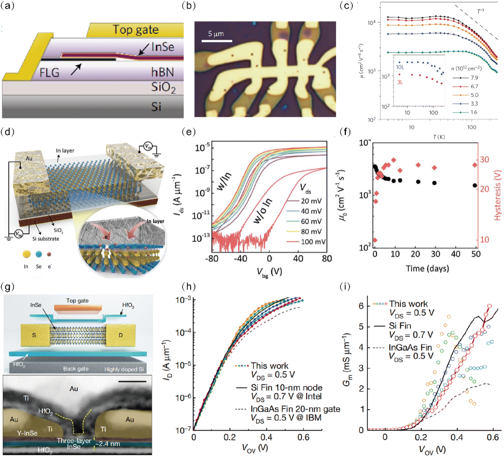 | ||
| Fig. 8 InSe field-effect transistor with the synergy of multiple optimization strategies. (a) Cross-sectional schematic and (b) optical micrograph of a FED device. The central bright area is the top gate that covers the encapsulated InSe. (c) T dependence of the Hall mobility μ for the 6 L InSe device. Reproduced with permission.37 Copyright 2017, Springer Nature. (d) Schematic illustration of the back-gate InSe FET device, packaged with an In layer as protective encapsulation and surface dopant for the layered InSe channel. (e) The transfer characteristics of a layered InSe FET with a 32 nm thick indium layer at different Vds. The results of a w/o In InSe FET were also recorded at Vds = 0.1 V for comparison. (f) The corresponding mobility and the window size of the hysteresis loop for the w/In InSe FET (32 nm thick In). Reproduced with permission.134 Copyright 2018, Wiley-VCH. (g) Schematic and transmission electron microscopy image of a double-gate InSe FET. (h) and (i) transfer characteristics and transconductance comparison of five typical ballistic 2D InSe FETs (coloured dots), a 10 nm-node silicon FinFET (Intel, solid black line) and 20 nm InGaAs FinFET normalized by state-of-the-art Fin Pitch = 34 nm (IBM, dashed black line). Reproduced with permission.135 Copyright 2023, Springer Nature. | ||
Additionally, Li et al.134 developed a robust InSe FET with excellent stability by depositing an indium layer (Fig. 8(d)). This indium interlayer served a dual purpose: reducing the contact barrier between the Au electrode and InSe while concurrently inducing a surface electron-doping effect that enhances mobility. The doping level of the InSe surface can be tuned by regulating the thickness of the In interlayer. As shown in Fig. 8(f), the optimized InSe FETs delivered unprecedented high electron mobility of up to 3700 cm2 V−1 s−1 at room temperature, which is comparable to state-of-the-art strained germanium (Ge) devices.2 Recently, Jiang et al.135 unveiled ballistic FETs with 2D InSe channels; the schematic and the cross-section high-resolution scanning transmission electron microscopy image of the device is shown in Fig. 8(g). The ballistic FETs with a channel length of 10 nm, a 2.6 nm thick HfO2 dielectric and yttrium-doped InSe (Y–InSe) were used as an interlayer between the Ti/Au electrodes and the channel material to establish the ohmic contact. A comparison between 2D InSe FETs, silicon with a 10 nm node, and InGaAs FinFETs with a 20 nm gate is shown in Fig. 8(h) and (i). The 2D InSe FETs exhibited a much lower supply voltage of 0.5 V and a record peak transconductance of 6 mS μm−1 at 0.5 V, which is the highest value of all reported low dimensional nanomaterial-based FETs and three times larger than that of InGaAs FinFETs. The top-gate stack and deposited gate metal protect the channel from moisture and oxygen, preserving the device stability. The ballistic ratios of this transistor reached more than 83%, which is the highest recorded for 2D based transistors and silicon FETs.136,137 In the above studies, through the synergistic effects of electrode optimization, structural refinement, and isolation from moisture and oxygen, remarkable high-performance InSe FETs were obtained comparable to silicon-based and germanium-based devices.138,139
Extensive research has been dedicated to fabricating high performance FETs with a primary objective of achieving enhanced mobility. The optimization of 2D FETs predominantly revolves around three pivotal strategies: the optimization of dielectric materials, surface encapsulation and contact electrodes. InSe FETs possess an ultrahigh on/off ratio and excellent mobility due to the synergistic effects of multiple optimization strategies, which suggest that the FETs can operate at a higher frequency and improve the switching speed. Meanwhile, InSe-based FETs have low power consumption in electronic applications due to the high mobility. The performance of InSe-based FETs with different device structures reported in the past decade are summarized in Table 4.
| Preparation method | Dielectric material/nm | h/nm | V D/V | V G/V | Mobility/cm2 V−1 s−1 | Ref. |
|---|---|---|---|---|---|---|
| a h: Thickness of InSe. | ||||||
| PLD | SiO2/300 | 20 | 0.1 | 20 | 70 | 81 |
| 1 | 0.1 | 20 | 10 | |||
| 5 | 0.1 | 20 | 50 | |||
| CVD | SiO2/300 | 1 Layer | 120 | 0–140 | 3 × 10⁻⁵ | 48 |
| ME/— | SiO2/300 | 9 | 0.1 | 80 | 102 | 138 |
| ME/Bridgman | SiO2/280 | 9.1 | 1 | 40 | 0.06 | 116 |
| 32 | ||||||
| CVD | SiO2/300 | 1 | 60 | 66.1 | 90 | |
| 1 | 60 | 2.2 | ||||
| 10 | ||||||
| CVD | SiO2/300 | 32 | 1 | 40 | 79.5 | 140 |
| ME/Bridgman | SiO2/100 | 20–40 | 1 | 50 | ∼100 | 119 |
| ME/— | SiO2/300 | 35 | 2 | 60 | 0.09 | 141 |
| ME/Bridgman | SiO2/285 | 30 | 2 | 40 | 32.6 | 142 |
| ME/— | SiO2/300 | — | 0.1 | 50 | ∼30–70 | 123 |
| ME/— | SiO2/300 | 35 | 0.1 | 15 | 249 | 143 |
| 20–80 | 0.1 | 15 | ∼150–250 | |||
| ME/— | SiO2/300 | 31 | 1 | 40 | 63.5 | 144 |
| ME/— | SiO2/100 | 51 | 2 | 10 | 185.8 | 145 |
| PLD | SiO2/300 | 15 | 1 | 10 | ∼0.1–0.55 | 91 |
| ME/— | SiO2/300 | 7 | 5 | 80 | 5 | 146 |
| ME/CVT | SiO2/300 | — | 0.1 | 60 | 122 | 139 |
| CVD | SiO2/300 | 35–40 | 1 | 40 | 125 | 121 |
| ME/— | SiO2/300 | 10–20 | 1 | 40 | ∼600(240 K) | 147 |
| 33 | 1 | 40 | 4.7–162 | |||
| PVT | SiO2/300 | 10 | 1 | 40 | 2 | 95 |
| 50 | 1 | 40 | 37 | |||
| ME/CVT | SiO2/300 | 100 | 1 | 6 | 450 | 89 |
| ME/CVT | SiO2/285 | 7–22 | 0.5 | 60 | 1 | 148 |
| ME/CVT | SiO2/290 | 13 | 5 | 80 | 32 | 128 |
| CVD | SiO2/290 | 24 | 40 | 10.32 | 18 | |
| ME/TGM | SiO2/300 | 8 | 1 | 60 | 11.16 | 149 |
| ME/— | SiO2/270 | 10–15 | 80 | 0.0116 | 150 | |
| ME/— | SiO2/300 | 10 | 1 | −60–60 | 31 | 133 |
| ME/— | SiO2/300 | 10 | -5–5 | -2–2 | 100.15 | 151 |
| ME/— | SiO2/300 | 10 | -5–5 | -5–5 | 11.5 | 151 |
| ME/— | SiO2/300 | 20 | 0.1 | −60–60 | 251.1 | 152 |
| CVD | PMMA/SiO2 200/300 | 34 | 1 | 60 | 395 | 90 |
| PMMA/Al2O3 200/50 | 33 | 1 | 8 | 1055 | ||
| Modified SiO2 (HMDS) | 20–40 | 1 | 50 | ∼200 | ||
| ME/Bridgman | PMMA/SiO2 200/100 | 20–40 | 1 | 50 | 1250 | 119 |
| Si3N4/100 | 20–40 | 1 | 50 | ∼50 | ||
| ME/Bridgman | h-BN/300 nm SiO2 | 10–15 | 1 | 60 | 450(2 K) | 132 |
| ME/— | h-BN/300 nm SiO2 | 0.1 | 50 | ∼440–470 | 123 | |
| ME/— | h-BN/10 | 15 | 0.1 | −40–80 | 904 | 153 |
| ME/— | h-BN | 10 | 1 | −15–15 | 1078 | 133 |
| ME/— | HfO2/30 | 35 | 0.1 | 1 | 128.7 | 143 |
| ME/— | hBN/SiO2300 | 10–20 | 1 | 80 | ∼400 (2 K) | 126 |
| 15.8 | 0.1 | 4 | 1146 | |||
| ME/CVT | h-BN/SiO2 10.8/100 | 14 | 0.1 | 4 | 1161 | 139 |
| 25.6 | 0.1 | 4 | 1149 | |||
| CVD | PMMA/AlO/HZO/SiO2 9/4/20/300 | 40 | 1 | 8 | 49 | 121 |
| PMMA/AlO/HZO/SiO2 50/4/20/300 | 40 | 1 | 8 | 246 | ||
| PMMA/AlO/HZO/SiO2 100/4/20/300 | 40 | 1 | 8 | 491 | ||
| PMMA/AlO/HZO/SiO2 200/4/20/300 | 40 | 1 | 8 | 863 | ||
| PMMA/SiO2 200/300 | 40 | 1 | 4 | 244 | ||
| AlO/HZO/SiO2 4/20/300 | 40 | 1 | 1.5 | 11 | ||
| 4 | 1 | 60 | 3 | |||
| ME/Bridgman | h-BN/SiO2 33/285 | 7.2 | 1 | 60 | 11 | 154 |
| 17.6 | 1 | 60 | 150 | |||
| 24.5 | 1 | 60 | 204 | |||
| ME/— | BCB/SiO2 100/270 | 10–15 | 1 | −80–80 | 688.2 | 150 |
| ME/— | Al2O3/20 | 41 | 1 | −10–10 | 19 | 155 |
| ME/— | Al2O3/28.6 | 6–10 nm | 0.1 | −50–50 | 15.7 | 156 |
| ME/— | PMMA/Al2O3 150/30 | 10 | 1 | −15–15 | 511 | 133 |
| ME/— | PMMA/Al2O3 150/30 | 10 | 1 | −15–15 | 761 | 133 |
| MACVD | h-BN | — | 5 | −70–70 | 6.3 | 157 |
| CVD | Ion gel | 1 Layer | 0.1 | 3 | 30 | 48 |
| ME/— | InSe oxidation layer/0.55 | 17 | 2 | 60 | 412 | 158 |
| ME/CVT | InSe oxidation layer | 13 | 0.1 | −30–30 | 1200 | 129 |
| ME/— | InSe superlattice/20–40 | 31 | 1 | −40–40 | 299.1 | 144 |
| ME/— | In/32 | 9 | 0.1 | −40–40 | 3700 | 138 |
| ME/— | ALD alumina encapsulation/35 | 35 | 2 | −60–60 | 100 | 141 |
| ME/CVT | Dry oxide InSe | 13 | 5 | 80 | 423 | 128 |
| ME/CVT | h-BN/8 | 10 | 0.1–1 | −20–20 | 728 | 159 |
| CuInP2S6 (CIPS)/70 | ||||||
| ME/— | PMMA/200 | 51 | 2 | −10–10 | 203.8 | 145 |
| ME/Bridgman | HfO2/0.9 | 50 | 0.1 | −15–15 | 42.2 | 160 |
| ME/— | Ionic liquid encapsulation | 10–20 | 3 | −20–20 | ∼700(200 K) | 147 |
| ∼500(240 K) | ||||||
| ME/— | PMMA/250 | 35 | 0.1 | −15–15 | 1206 | 143 |
| 20–80 | ∼900–1200 | |||||
| ME/— | OML/1 | 10–20 | 1 | −50–50 | 940 | 126 |
| ME/Bridgman | In/3 | 10–15 | 1 | −20–20 | 1000 | 132 |
| ME/— | Se encapsulation | 30 | 1 | -5–5 | ∼900–2500 | 161 |
| Al2O3/30 | 4–65 | 1 | -5–5 | ∼10–110 | ||
| ME/— | PMMA/250 | 37.3 | 1 | −10–10 | 246 | 162 |
| ME/CVT | h-BN/30–40 | 8–12 | 0.5 | −60–60 | 30–120 | 148 |
| ME/CVT | P(VDF-TrFE)/300 | 18 | 0.1 | −40–40 | 272.9 | 163 |
| ME/— | DDAB functionalization of InSe | 10–15 | −80–80 | 2785 | 150 | |
| ME/— | h-BN | 1–10 layer | 1 | 10 | ∼1000 | 164 |
4.2 InSe optoelectronic devices
Optoelectronic devices, which can convert optical signals into electrical signals or vice versa, play a pivotal role in various fields like communications, optical displays, environmental monitoring, biological sensing, optoelectronic memory, etc.49,142,165–167 Over the past decade, photodetectors based on two dimensional materials have drawn significant attention and development.168 Due to the suitable direct band gap, ultrahigh carrier mobility and pronounced light–matter interaction, InSe exhibits extraordinary potential for next generation optoelectronic devices, especially in photodetectors.23,37,169In the last ten years, a myriad of InSe-based photodetectors have been explored. Yet, there remains a noticeable gap between fundamental research and their transition to mature applications. Tamalampudi et al.170 and Lei et al.171 were pioneers in fabricating InSe photodetectors with SiO2 dielectric substrates and Au symmetrical contact electrodes. Their groundbreaking research resulted in initial photoresponsivity values of 34.7 mA W−1 (532 nm), 12.3 A W−1 (450 nm) and 3.9 A W−1 (633 nm). Based on this work, subsequent research has introduced various strategies to enhance photodetection performance or augment the functionality of 2D materials, such as the optimization of metal contact, modification and tailoring of channel materials, doping, encapsulation, and the design of innovative device architecture.
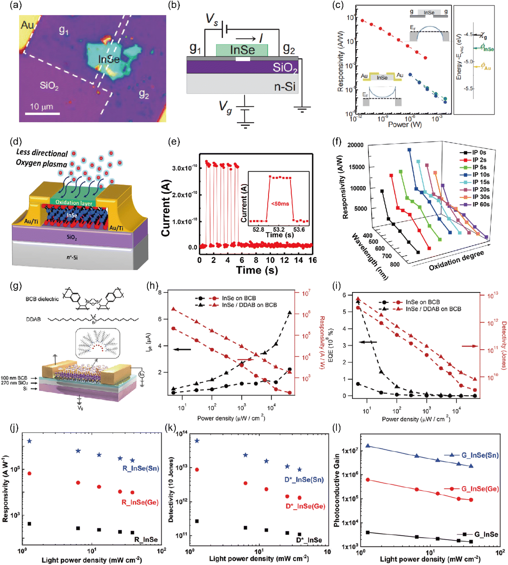
To properly modulate the InSe–metal electrode barrier height, contact engineering of various metals and semiconductors can be utilized to modify the Fermi level along with the band structure. Mudd et al.172 employed monolayer graphene as the electrode, fabricating a planar Gr-InSe–Gr photodetector (as shown in Fig. 9(a and b)). Given that the electron affinity of graphene exceeds that of InSe, electrons at equilibrium tend to transfer from graphene to InSe, where they can form an accumulation layer at the interface between graphene and InSe. As a result, the graphene/InSe interface facilitates electron injection because of the formation of the ohmic contact. In contrast, the large Schottky barrier of the Au/InSe interface obstructs electron transport. Notably, the Gr–InSe–Gr photodetector exhibits remarkable responsivity and EQE of 4 × 10³ A W−1 and 5 × 10⁵% under 633 nm light illumination (Fig. 9(c)). Subsequently, Yang et al.89 designed a 2D InSe photodetector using the focused ion beam (FIB) technique, incorporating a symmetric Pt electrode with low contact resistance. It was confirmed that during FIB processing, a conducting amorphous alloy layer was embedded between the Pt electrode and the semiconductor interface. In addition, the ion bombardment on the semiconductor surface prevented the formation of a Schottky barrier as well as eliminated surface contaminants and native oxides on the semiconductors.96 InSe photodetectors with low contact resistance fabricated on the FIB exhibited unparalleled responsivity and detectivity of up to 1.8 × 10⁷ A W−1 and 1.1 × 10¹⁵ Jones for UV light. This value is much higher than what is commonly observed in other 2D material-based photoconductors and phototransistors. Current research on the optimization of electrode contact for InSe electronic devices reveals that Au predominantly forms Schottky contact with InSe nanoflakes, while graphene, metallic Ag and In result in ohmic contact.131,173
 | ||
| Fig. 9 InSe photodetector with different optimization strategies. (a) Optical image and (b) schematic structure of a graphene–n-InSe–graphene planar device on a gated SiO2/Si substrate. (c) Photoresponsivity versus incident laser power at T = 300 K and λ = 633 nm for planar device geometries based on graphene/InSe/graphene (top) and Au/InSe/Au heterostructures (bottom). Reproduced with permission.172 Copyright 2015, Wiley-VCH. (d) Schematic representation of indirect incident plasma treatment on an InSe FET. (e) Photoresponse cycles of the InSe FET by SOD (strongly oxidized) under light illumination. (f) Photoresponsivity of the InSe phototransistors with different oxidation degrees and different illumination wavelengths. Reproduced with permission.158 Copyright 2017, American Chemical Society. (g) Illustration of device structure and the chemical structure of BCB polymer and DDAB molecule. (h and i) Power dependence of (h) photocurrent and responsivity and (i) EQE and detectivity of InSe on SiO2, InSe on BCB, and InSe/DDAB on BCB at Vg = 0 V and Vds = 1 V illuminated with 365 nm light. Reproduced with permission.117 Copyright 2021, Wiley-VCH. (j–l) Illumination dependence (j) responsivity (R), (k) detectivity (D*) of as-prepared pure InSe, InSe (Ge), and InSe (Sn) photodetector measured under the applied bias of 1 V, (l) power dependence of photoconductive gain. Reproduced with permission.175 Copyright 2022, Wiley-VCH. | ||
Various types of surface modification, including oxygen treatment and molecular functionalization, play a pivotal role in elevating optoelectronic performance. Chang et al.158 presented an InSe-based ultrahigh gain photodetector utilizing the surface oxidation doping (SOD) method. With exposure to oxygen plasma, a dense, thin amorphous layer with a smooth and uniform surface formed on the top of the crystalline InSe flake, which doped the underlying InSe with holes and produced a gradient of carrier concentration through surface charge transfer (Fig. 9(d)). The SOD-induced carrier concentration gradient prompted the formation of a vertical built-in potential and band bending within the InSe layers, resulting in efficient separation of photogenerated electron–hole pairs under light illumination. As a result, the improved InSe photodetector demonstrated an ultrafast response time of <50 ms and ultrahigh responsivities of 5 × 10⁶ A W−1 under 365 nm light illumination (Fig. 9(e and f)). In a divergent strategy, Wang et al.117 developed an InSe-based detector with molecular functionalization decorated InSe materials, demonstrating an improvement strategy through the use of a common surfactant molecule called didodecyldimethylammonium bromide (DDAB) (Fig. 9(g)). Molecular functionalization effectively filled the defect states that were generated during the synthesis of InSe crystals and the delamination by mechanical exfoliation. The healing of Se vacancies by DDAB helped to restore the crystal structure, thereby suppressing the recombination of photo-generated charges in vacancy traps. The performance of the detector treated by DDAB enhanced the responsivity up to 106 A W−1, EQE approaching 108%, and detectivity of 1013 Jones within the wavelength range of 300 nm to 690 nm (Fig. 9(h and i)). Furthermore, manipulating the surface molecular doping of 2D InSe materials allows the realization of n-type doping in InSe.
Beyond post-processing surface doping, precise doping during InSe crystal growth remains instrumental in modulating optical and electrical properties achieving desired performance characteristics. Hao et al.174 studied the performance of a Gr/InSe photoconductor based on S-doped InSe nanoflakes. Their observations revealed that defect states introduced by S atoms induce an increase in photon absorption and the subsequent electron–hole pair generation, consequently boosting the electron injection from InSe to graphene and increasing the overall photocurrent. The photodetection responsivity of InSe0.9S0.1 nanoflakes reached 4.9 × 10⁶ A W−1. In general, controlling dopants and their concentrations can augment the performance of photodetectors and enable multifunctionality since dopant-induced trap states are essential in determining the optoelectrical properties of semiconductors. Recently, Liao et al.175 reported the performance of an InSe photodetector based on Ge and Sn-doped InSe, revealing the mechanism of persistent photoconductivity in InSe. Photogenerated carriers are trapped in Ge or Sn shallow impurity states, improving the optoelectrical performance of pristine InSe. Ge and Sn-doped InSe devices exhibited pronounced photoconductive gains and maximized photocurrent. The Sn-doped InSe device achieved a maximum responsivity of around 1.7 × 10⁶ A W−1 under red light and a detectivity of 6.18 × 10¹³ Jones (Fig. 9(j and k)). To date, the highest responsivity of 2D InSe photodetectors has reached 107 A W−1, surpassing the performance standard of commercial photodetectors.89
The performance and design of photodetectors are intrinsically linked to several pivotal parameters.176 Metrics like photoresponsivity (R), response time (t), external quantum efficiency (EQE), detectivity (D), noise equivalent power (NEP), gain, photocurrent density (IP), dark current density (ID), on–off ratio, etc. are essential considerations in assessing the efficacy of 2D photodetectors.177 Although integrating an amplifier circuit can improve the optical response signal in scenarios of feeble photoresponsivity, the signal to noise ratio, which determines the sensitivity of the photodetector and the response time of the device, cannot be optimized through signal processing. The response time describes the speed of the photodetector and includes the rise time (trise) and the decay time (tdecay) of the charge carriers. More and more 2D InSe photodetectors have been reported over the past decade, a comprehensive overview of the performance of InSe-based photodetectors along with their respective structural details is summarized in Table 5.
| Preparation method | Device structure | h/nm | Wavelength/nm | Responsivity/A W−1 | Response time/ms | D*/Jones | Ref. |
|---|---|---|---|---|---|---|---|
| a h: thickness of InSe. | |||||||
| ME/Bridgman | Cr/Au–InSe–Cr/Au | 30 | 254 | 5.68 × 10⁴ | 5 | ∼2 × 10¹³ | 142 |
| Gr–InSe–Gr | 30 | 633 | 4 × 10³ | 1 | 1010 | 178 | |
| ME/Bridgman | Au–InSe–Au | 30 | 633 | 10−3 | — | — | |
| ME/Bridgman | In–InSe (with Au particle)–Au | 30 | 365 | ∼0.369 | 23 | ∼1011–1013 | 179 |
| ME/Bridgman | Cr/Au–InSe–Cr/Au | 12 | 633 | 12.3 | 40–50 | 1.07 × 10¹¹ | 180 |
| ME/Bridgman | Cr/Au–InSe–Cr/Au | 10 | 488 | 116 | — | 1011 | 169 |
| ME/Bridgman | Ti/Au–InSe–Ti/Au | 41 | 455 | 274 | 15 | 5.49 × 10¹² | 181 |
| ME/Bridgman | Ag–InSe–Au | 14 | 532 | 200.4 | 0.047 | 1.3 × 10¹⁵ | 182 |
| ME/Bridgman | Cr/Au–InSe–Cr/Au | 5–22 | 530 | 0.09 (vacuum) | 40 | — | 116 |
| 0.002 (in air for 20 h) | |||||||
| 405 | 1000–3500 (vacuum) | 77000 |
∼0.8–6.3 × 10¹³ | ||||
| 100–600 (1 h in air) | |||||||
| 1–10 (11 h in air) | |||||||
| ME/CVD | Cr/Au–InSe–Cr/Au | 6–24 | 490 | 12 × 104 | — | 7 × 10¹⁴–1015 | 18 |
| 600 | 11 × 104 | ||||||
| 700 | 10 × 104 | ||||||
| 850 | 4 × 10⁴ | ||||||
| CVD | Au–InSe–Au | 165 | 450 | 1.49 × 10³ | — | 5.35 × 10¹² | 183 |
| 364 | 530 | 2.61 × 10³ | 4.26 × 10¹² | ||||
| 562 | 660 | 1.16 × 10³ | 1.06 × 10¹³ | ||||
| ME/CVT | Ti/Au–InSe–Ti/Au | 32 | 325 | 1.8 × 10⁷ | 1.1 × 10¹⁵ | 89 | |
| 532 | 2.4 × 10⁶ | 12000 |
1.4 × 10¹⁴ | ||||
| 633 | 6.4 × 10⁵ | 7000 | 4.2 × 10¹³ | ||||
| 38 | 325 | — | 10000 |
— | |||
| ME/CVT | Cr/Au–InSe–Cr/Au | 18 | 532 | 14250 |
0.600 | 1.63 × 10¹³ | 163 |
| ME/CVT | In–InSe–In | 14 | 850 | ∼5–20 | — | — | 184 |
| FLGr–InSe–FLGr | 14 | 850 | 80–100 | — | 2 × 10¹¹ | ||
| Bottom h-BN–Ti/Au–FLG–AuCl3 doped InSe–top FLG–Ti/Au-top h-BN | 14 | 470 | 19300 |
— | 3 × 10¹³ | ||
| 980 | 7870 | 1.5 × 10¹³ | |||||
| Bottom h-BN–Ti/Au–bottom FLG | 14 | 850 | ∼200–400 | — | — | ||
| AuCl3 doped InSe top FLG–Ti/Au | |||||||
| Bottom h-BN–Ti/Au–bottom FLG | 14 | 850 | ∼500–1000 | — | — | ||
| AuCl3 doped InSe top FLG–Ti/Au–top h-BN | |||||||
| PLD | Au–InSe–Au | 1–20 | 980–370 | 0.1–27 | 500 | — | 81 |
| PVD | Cr/Au–InSe–Cr/Au | few-layer | 532 | ∼6 | — | — | 79 |
| ME/TGM | Ti/Au–InSe–Ti/Au | 4–10 | 532 | 4.7 × 10⁻³ | — | — | 171 |
| ME/TGM | Ti/Au–InSe–Ti/Au | 7 | 532 | ∼1–16 | — | — | 146 |
| ME/TGM | Cr/Au–InSe–Cr/Au | 8 | 800 | 194 | ∼0.620 | 1.45 × 10¹² | 149 |
| 2 × 10³–4 × 10⁴ | 22 | 4 × 10¹⁰–1 × 10¹² | |||||
| LPE/TGM | Cr/Au–InSe nanosheet–Cr/Au | 40–100 | 515.6 | ∼103–5 × 10⁷ | 0.450 | — | 155 |
| Cr/Au–InSe film–Cr/Au | 41 | 515.6 | 10 | 3000 | — | ||
| ME/— | Cr/Au–graphene–InSe–graphene–Cr/Au | 20 layer | 532 | ∼1 × 10²–0.94 × 10³ | — | — | 185 |
| Cr/Au–InSe–Cr/Au | 4–5 layer | 532 | 5 × 10⁻²-0.101 | — | — | ||
| ME/— | Al–InSe–Al | 543 | — | 60000 |
— | 186 | |
| Al–InSe (with Al nanodisk)–Al | ∼510 | 543 | — | 0.087 | — | ||
| Ti/Au–InSe–Ti/Au | — | 543 | — | 0.27 | — | ||
| ME/— | Ti/Au–InSe–Ti/Au | 35 | 500 | 700 | 4800 | 2 × 10¹³ | 187 |
| Gr–InSe–Gr | 33 | 500 | 60 | 0.128 | 2.5 × 10¹² | ||
| 1000 | 5.3 | ||||||
| 600 | ∼48 | ||||||
| 800 | ∼13 | ||||||
| Gr–InSe–Gr | 33 | 500 | 1.57 | 0.310 | — | ||
| ME/— | Ti/Au–InSe (O2 plasma)–Ti/Au | — | 365 | 5 × 10⁶ | — | — | 158 |
| 530 | 5 × 10⁵ | ||||||
| Ti/Au–InSe–Ti/Au | — | 365 | ∼12500 |
— | — | ||
| 530 | ∼7000 | ||||||
| 850 | ∼5000 | ||||||
| ME/— | Au–InSe–Au | ∼33 | 400 | 0.416 | 0.222 | 8.7 × 10¹¹ | 15 |
| 650 | 0.0249 | ||||||
| ME/—ME/— | Cr/Au–InSe superlattice–Cr/Au | 31 | 700 | 1.7 × 10⁴ | — | 1.4 × 10¹³ | 144 |
| Cr/Au–InSe–Cr/Au | 31 | 700 | 2.0 × 10³ | — | 9.1 × 10¹² | ||
| ME/— | Ti/Au–InSe–Ti/Au-PMMA200 | 51 | 450 | ∼50–250 | — | ∼2 × 10⁹–1 × 10¹⁰ | 145 |
| Ti/Au–InSe–Ti/Au | 70 | 450 | ∼150–650 | — | ∼6 × 10⁹–3 × 10¹⁰ | ||
| ME/— | Cr/Au–InSe–Cr/Au | 10–15 | 365 | 10−3 | 288 | ∼108 | 117 |
| BCB-Cr/Au–InSe–Cr/Au | 10–15 | 365 | ∼5 × 10²–2 × 10⁵ | 17.33 | ∼7 × 10⁹–2 × 10¹² | ||
To enhance the response speed or sensitivity of photodetectors, novel architecture of photodetectors was designed especially to improve the charge carrier collection rate. Lei et al.186 introduced the avalanche effect in an Al–InSe–Al photodetector by creating large Schottky barriers between InSe and the aluminum electrodes. When subjected to a large electric field, carriers in the channel can attain a sufficiently high kinetic energy to generate electron–hole pairs via collision or impact ionization. The initial electron–hole pairs are generated under light illumination and separated by an electric field applied to the device. The avalanche photodetector geometry improved the external quantum efficiency to 344% and achieved a response time of 60 μs. In recent years, Yang et al.188 fabricated an InSe-based photodetector incorporating a two dimensional metallic material of transition-metal carbides Ti2CTx, serving as the electrode and plasmonic grating structure. Due to the high work function (4.9 eV) of the Ti2CTx electrode, a Schottky barrier was formed at the InSe/Ti2CTx interface, effectively suppressing the dark current and allowing the application of a sufficiently high drain voltage to trigger the avalanche effect, as shown in Fig. 10(a). The InSe/Ti2CTx photodetector exhibited high performance from the visible to the NIR wavelength, achieving a high responsivity of 1.1 × 10⁴ A W−1, a high detectivity of 7.1 × 10¹¹ Jones, and a short response time of 0.8 ms. Furthermore, Ti2CTx with high conductivity was exploited as an electrode with additional plasmonic structures that could enhance the light absorption of InSe nanoflakes, specifically by patterning Ti2CTx nanoribbon arrays with the plasmonic effect. The InSe/Ti2CTx photodetector exhibited excellent performance with a shorter response time of 0.5 ms (Fig. 10(b)), higher responsivity of 1 × 10⁵ A W−1 (Fig. 10(c)) and higher detectivity of 7.3 × 10¹² Jones. This work is similar to previous reports of patterned Al nanodisks and Au nanoribbons,179,186,189,190 where patterned plasmonic structures improved light absorption in two-dimensional materials. This geometry allows the photodetector to exhibit enhanced responsivity and detectivity without sacrificing the response speed.
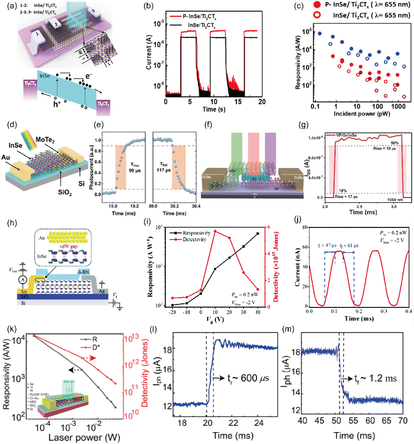 | ||
| Fig. 10 InSe-based photodetectors with an innovative heterostructure. (a) Schematic of the InSe/Ti2CTx photodetector structure and avalanche effect under light illumination. (b) Light current and dark current as a function of gate voltage and (c) responsivity as a function of incident light power for the patterned and unpatterned InSe/Ti2CTx photodetector. Reproduced with permission.188 Copyright 2019, American Chemical Society. (d) Schematic structure of the MoTe2/InSe under laser irradiation. (e) Response time of the device under 520 nm with light power densities of 20 mW cm−2 at Vds = 0 V. Reproduced with permission.192 Copyright 2024, Wiley-VCH. A schematic diagram (f) and (g) the dynamic response speed of the VP/Gr/InSe device under laser light irradiation. Reproduced with permission.194 Copyright 2024, American Chemical Society. (h) Schematic diagram of the vdW Schottky junction device with Au–Ag asymmetric metal contacts. (i) Photoresponsivity and detectivity versus the gate-voltage Vg under 0.2 nW illumination. (j) Time-resolved photoresponse of the device at Vbias = −2 V. Reproduced with permission.173 Copyright 2020, Royal Society of Chemistry. (k) Schematic device structure of a multilayered InSe photodetector under monochromatic light beam illumination (l) and (m) time-resolved photo switching behavior of the InSe phototransistor in the polarization-up state. Reproduced with permission.163 Copyright 2020, American Chemical Society. | ||
On the other hand, vdW heterostructures present a novel strategy for preparing optoelectronic devices with multiple functions and excellent performance. Two dimensional InSe materials have been employed in the construction of heterostructure devices to improve the performance of photodetectors both in terms of high responsivity and ultrafast response time. These advancements encompass both p–n heterojunctions and Schottky junctions. As the most typical representative of the graphene/InSe system, which exhibits high conductivity properties thanks to the absence of Schottky barrier at the graphene/InSe interface. Chen et al.185 constructed a vertical geometry heterostructure photodetector of graphene/few-layer InSe, which exhibited significantly improved performance due to the electronic structure of the heterointerface. This structure efficiently facilitated electron transfer to the graphene and modulated the carrier density of graphene. Concurrently, the graphene layer acted as a protective shield for ultrathin InSe, which is chemically unstable under ambient conditions. Consequently, the InSe/Gr-based photodetector showcased an excellent responsivity of 0.94 × 10³ A W−1.
Subsequently, various heterostructure photodetectors have been revealed with a significantly enhanced performance. For instance, Feng et al.191 fabricated a photodetector with the vertical geometry of GaTe–InSe van der Waals (vdWs) p–n heterojunction, where a swift response time of 20 μs was achieved and was attributed to the stable and fast carrier transfer via the built-in electric field in the depletion region. However, the zero-biased photodetector exhibited a slightly diminished responsivity of 13.8 mA W−1. Recently, He et al.192 constructed a self-powered photodetector based on an MoTe2/InSe van der Waals heterostructure (vdWH) device as shown in Fig. 10(d), which exhibited an excellent responsivity (R) of 433.88 mA W−1 and a specific detectivity (D*) of 1.65 × 10¹² Jones under 405 nm irradiation. Meanwhile, a fast response speed of 99 μs and a broadband response range from 405 to 980 nm were achieved, which is originating from a strong built-in electric field at the MoTe2/InSe heterostructure interface (Fig. 10(e)). Furthermore, Gao et al.193 developed a hybrid vdW heterostructure photodetector with vertically stacked graphene, the transition metal dichalcogenide WSe2, and the III–VI semiconductor InSe. This heterostructure photodetector exhibited a decent responsivity of 83 A W−1, a high detectivity of 1.55 × 10¹² Jones, and a fast response time of 36 ms. Recently, Ahmad194 presented a violet phosphorus (VP)/Gr/InSe vdW heterostructure near-infrared polarization photodetector as shown in Fig. 10(f). VP and InSe act as the drain and source, respectively, and a few layers of graphene were inserted between the heterostructure of VP/InSe to manipulate the structure geometry, boost the photoinduced charge carrier, and suppress the dark current. The VP/Gr/InSe heterostructure device showed a high responsivity of 230 A W−1, detectivity of 4.64 × 10¹³ Jones, and a fast response speed of 17 μs at a wavelength of 1064 nm (Fig. 10(g)). To improve the stability of the VP/Gr/InSe device, capping the device with a few layers of h-BN is efficient for protecting it from degradation.
Meanwhile, researchers shifted the spotlight to InSe alloy compounds; p–n heterojunction photodetectors based on InSe and its alloy compounds have also achieved excellent performance. Yu et al. studied the optoelectronic properties of p–n heterojunctions consisting of InSe and InSe alloys, such as InSe–InSe0.82Te0.18195 and InSe–In0.24Ga0.76Se196 p–n heterojunctions. The electrical transport properties of InSe alloys correlate with the content of Te or Ga composition; with the increasing ratio of Te or Ga, the intrinsic n-type electron transport behavior of InSe gradually transitioned to p-type hole transport behavior. More importantly, this type of van der Waals heterojunction device was demonstrated as a photodiode and self-powered photodetector (SPPD), showing stable and high-speed operation.
In addition to the p–n heterojunctions, the Schottky junctions are pivotal components in both microelectronic and optoelectronic devices. Hu et al.173 constructed an InSe photodetector with a Schottky junction by mechanically stacking an Au electrode onto multilayer InSe nanoflakes. In addition, multilayer h-BN flakes were integrated to envelop the InSe channel to protect the device from degradation. The structure is shown in Fig. 10(h), where the Schottky and the ohmic contact were formed at the interfaces of Au–InSe and Ag–InSe, respectively. Leveraging this asymmetric contact electrode, the Au–InSe–Ag photodetector exhibited a high detectivity over 2.4 × 10¹⁵ Jones, a high responsivity of 853 A W−1 and a fast response speed of 47 μs (Fig. 10(i and j)). Recently, Liu et al.197 constructed a single two-terminal opto-sensor based on a Schottky junction, with photocarrier separation induced by the built-in electric field between multilayer γ-InSe flakes and gold electrodes. It demonstrated broadband light-sensing image adaptation from the the ultraviolet to the near-infrared regime and fast response in self-powered mode. This simplified device exhibited the synergy of photo-pyroelectric and photo-thermoelectric effects, which exhibited good human-eye-like adaptation behaviors. This study may promote the development of advanced optoelectronic devices and artificial visual systems.
In recent years, there has been great interest in fabricating a multifunctional device by integrating different functional elements into a single device. Liu et al.163 fabricated InSe photodetectors using ferroelectric poly (vinylidene fluoride–trifluoroethylene) (P(VDF–TrFE)) copolymer films as the top-gate dielectric and h-BN as the bottom substrate (Fig. 10(k)), benefiting from the successful suppression of the dark current down to 10−14 A in the InSe channel. This was achieved by harnessing three different polarization states in ferroelectric P(VDF–TrFE) to tune the carrier transport of InSe and improve the interfacial properties. Consequently, the ferroelectric-gate InSe photodetectors demonstrated a high on/off ratio of over 108, a high responsivity up to 14250 A W−1, a high detectivity up to 1.63 × 10¹³ Jones, and a fast response time of 600 μs even at zero gate voltage (Fig. 10(l and m)). Furthermore, Inbaraj et al.198 reported an advanced device for both visible and IR photodetection, consisting of a 2D heterostructure (InSe/WSe2) and a P(VDF-TrFE) dielectric in a single device. The InSe/WSe2 heterostructure top-gated with the P(VDF-TrFE) dielectric demonstrates an ambipolar transfer behavior, and the ferroelectric polarization effect enhances photoresponsivity up to 104 A W−1 (λ = 633 nm). On the other hand, through the coupling between pyroelectricity and built-in electric field across the heterojunction, the detectivity could reach 1011 Jones (λ = 980, 1064 nm). The proposed device can promote the application of InSe for IR photodetection and provide a design for advanced application.
Extensive efforts have been made to improve the properties and expand the range of detection of 2D vdW heterostructures. In recent years, 2D/3D mixed-dimensional vdW optoelectronic devices have been successfully constructed. Yang et al.199 reported broadband self-powered photodetection based on the hybrid 3D Ge/2D γ-InSe van der Waals heterojunction. A built-in electric field is introduced at the hetero-interface of p-Ge/n-InSe to reduce the dark current and accelerate carrier separation. With a photoresponse range from 400 to 1600 nm, the device exhibits a high responsivity of 9.78 A W−1, detectivity (D*) of 5.38 × 10¹¹ Jones, and a fast response speed of 46 μs under a 1550 nm laser. Coincidently, Miao et al.200 proposed a robust self-powered optoelectronic device based on the 2D InSe/3D GaN heterojunction. An n type InSe film was epitaxially grown on a p type GaN substrate, with an atomically thin amorphous layer at the InSe/GaN interface as a charge trap. Thus, the response time is prolonged to 103 ms due to the charge traps, and this optoelectronic device can achieve information perception from visible to near-infrared. These results provide a new platform of 2D/3D heterostructures for advanced optoelectronic devices that may find applications in the post-Moore era.
InSe-based photodetectors exhibit excellent performance, their performance and functionalized application can be improved through different strategies like channel treatment, contact electrode optimization and device architecture optimization. van der Waals heterostructures enable bandgap engineering of different two-dimensional materials to realize the interlayer transition via band alignment. This structure not only accelerates the separation of carriers but also broadens the spectrum which is beyond the cut-off wavelength of individual two-dimensional materials. Detailed statistics of the performance of InSe-based photodetectors is summarized in Table 6.
| Device structure | h/nm | Wavelength/nm | Responsivity/A W−1 | Response time/ms | D*/Jones | Ref. |
|---|---|---|---|---|---|---|
| a h: Thickness of heterostructure materials. | ||||||
| Cr/Au–Gr/InSe–Cr/Au | 0.34/16 | 532 | 0.94 × 10³ | — | — | 185 |
| Ti/Au–oxide layer/InSe–Ti/Au | 2/17 | 365 | 5 × 10⁶ | — | — | 158 |
| 530 | 5 × 10⁵ | — | — | |||
| Au–Gr/InSe/MoS2–Au | 0.34/40/6 | 532 | 0.11 | <1 | 1.08 × 10¹⁰ | 201 |
| Cr/Au–GaTe/InSe–Cr/Au | 18/10— | 405 | 0.0138 | 0.02 | — | 191 |
| Gr–InSe/WSe2–Gr | 64.9/120.26 | 532 | 83 | — | 1.55 × 10¹² | 193 |
| Ti/Au–BP/InSe–Ti/Au | — | 633 | 0.01 | 24 | — | 202 |
| Cr/Au–BP/InSe–Cr/Au | 12/16 | 655 | 53.8 | 22 | 203 | |
| 1550 | 43.11 | — | ||||
| Au–P–Ti2CTx/InSe–Au | 5/20 | 405 | 1 × 10⁵ | 0.5 | 7.3 × 10¹² | 188 |
| Au–Ti2CTx/InSe–Au | 5/20 | 405 | 1.1 × 10⁴ | 0.8 | 7.1 × 10¹¹ | |
| Cr/Au–P(VDF–TrFE)/InSe–Cr/Au | 300/18 | 532 | 14250 |
0.6 | 1.63 × 10¹³ | 163 |
| Cr/Au–InSe/Te–Cr/Au | 42/120 | 400 | 0.45 | 0.6 | 1.1 × 10¹³ | 204 |
| In/Au–InSe/Se–In/Au | 30/1000 | 460 | 0.032 | 30 | 1.7 × 10¹¹ | 205 |
| Cr/Au–InSe/InSeTe–Cr/Au | 20–70 | 900 | 0.014 | 120 | — | 195 |
| Cr/Au–InSe/InGaSe–Cr/Au | 24/45 | 400 | 49 | 180 | 1012 | 196 |
| FLG-InSe/AuCl3 doped InSe-FlG | 16 | 470 | 19300 |
— | 3 × 10¹³ | 184 |
| 980 | 7870 | 1.5 × 10¹³ | ||||
| Ti/Au-GeAs/InSe–Ti/Au | 90/20 | 635 | 0.357 | 25 | 2 × 10¹¹ | 206 |
| 405 | 1.2 | — | — | |||
| Ti/Au-ReS2/InSe–Ti/Au | 5/15 | 365 | 1921 | 21.6 | 6.51 × 10¹³ | 207 |
| Cr/Au–InSe/SnSe–Cr/Au | 77.6/84.7 | 808 | 0.35 | 260 | 5.8 × 10¹⁰ | 208 |
| Ti/Au-Gr/InSeS–Ti/Au | — | 700 | 4.9 × 10⁶ | 41 | — | 174 |
| Ni/Au-VO2/InSe–Ni/Au | 12.5/65 | 405 | 6.15 | 9.7 | 2.19 × 10¹³ | 209 |
| Cr/Au–Ge/InSe–Cr/Au | 121/350000 |
1550 | 9.78 | 0.046 | 5.38 × 10¹¹ | 199 |
| Cr/Au-VP/InSe–Cr/Au | 10/18 | 1064 | 182.8 | 0.027 | 7.86 × 10¹² | 194 |
| 10/18 | 532 | 21.8 | 9.3 × 10¹¹ | |||
| Cr/Au-VP/Gr/InSe–Cr/Au | 10/Gr/18 | 1064 | 230 | 0.017 | ∼1013 | |
| Cr/Au–MoTe2/InSe–Cr/Au | 39.8/38.8 | 405 | 0.433 | 0.099 | 1.65 × 10¹² | 192 |
| 39.8/38.8 | 405 | 13.5 | 7.4 × 10¹⁰ | |||
| Cr/Au–InSe/WSe2–Cr/Au | 21/19 | 633 | 104 | 200 | ∼1011 | 198 |
| Cr/Au-Gr/InSe–Cr/Au | Gr/45 | 532 | 2.17 × 10² | 0.314 | 3.78 × 10¹³ | 210 |
| Gr/12 | 532 | 2.12 × 10⁴ | 0.241 | 1.73 × 10¹⁴ | ||
| Ag–InSe/GaN–Ag | 8/20 | 300–400 | 0.105 | 5 | ∼1014 | 200 |
| Cr/Au–InSe/Te–Cr/Au | 20/50 | 450 | 0.07 | 0.340 | 3.73 × 10¹⁴ | 152 |
| Ni/Au–Bi2O2Se/InSe–Ni/Au | 7/332 | 405 | 0.0752 | 5.8 | 1.08 × 10¹² | 211 |
| 7/332 | 980 | 0.0133 | 2.06 × 10¹¹ | |||
In general, research has revealed significant performance disparities in electronic and optoelectronic devices made from two-dimensional InSe materials. To illustrate this observation, the characteristics of InSe-based field effect transistors and photodetectors at room temperature are consolidated in Tables 4 and 5, and further visualized in Fig. 11. Taking mobility as an example, a comprehensive dataset for few-layer InSe is shown in Table 4, which is also graphically displayed in Fig. 11(a). Notably, the observed mobility covers a remarkable range of eight orders of magnitude, from 3 × 10⁻⁵ cm2 V−1 s−1 to 103 cm2 V−1 s−1, the highlighted circles represent the average values of mobility data for each column. In addition, the photoresponsivity and response speed of the photodetector are also highly scattered, as shown in Table 5 and Fig. 11(b), photoresponsivity values fluctuate significantly. The photoresponsivity reaches 107 A W−1 at λ = 515.6 nm, while the lowest reported one is 34.7 mA W−1 at λ = 532 nm, with a difference of 9 orders of magnitude. Equally fascinating is the divergence in response time, the response time ranges from an ultrafast 87 μs to a comparatively slow 5.63 s, with a difference of almost 5 orders of magnitude, as shown in Fig. 11(c). Obviously, it is evident that there remains ample scope for refining the stability and reliability of two-dimensional InSe materials and devices.
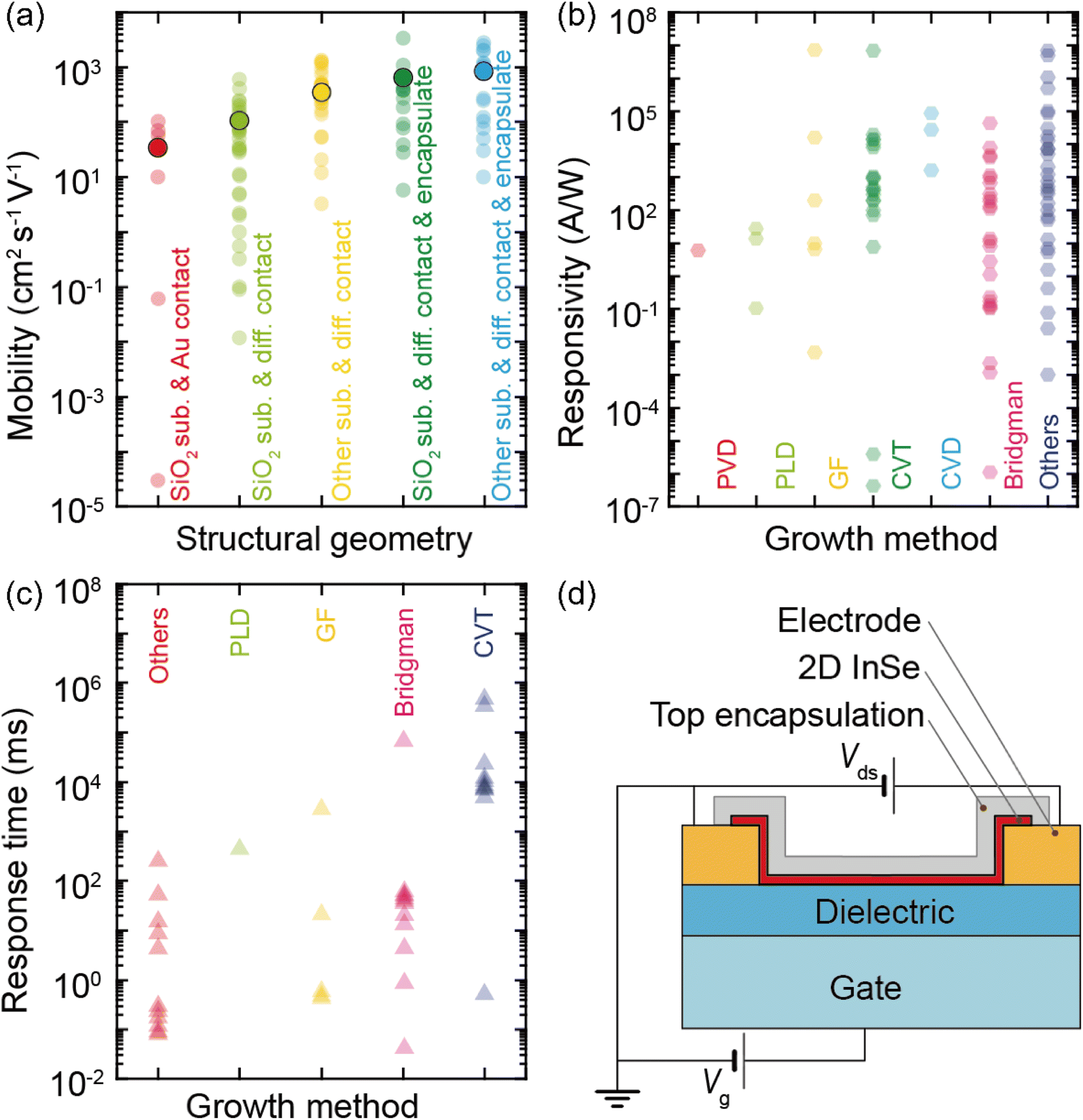 | ||
| Fig. 11 Statistical analysis of the reported characteristics of 2D InSe based devices and their structural geometry: (a), (b) and (c) statistical distribution of the electrical mobility of field effect transistors (FETs), photoresponsivity and response time of photodetectors based on 2D InSe, (d) typical structural geometry of 2D InSe devices. | ||
4.3 Other applications
As mentioned previously, the emerging 2D semiconductor InSe nanoflakes have unquestionably captured increasing interest in the field of electronic and optoelectronic devices due to their record-breaking carrier mobility and photoresponsivity. In recent years, 2D InSe has carved out a niche in the field of strain engineering and flexible electronics due to its very low Young's modulus of 23.1 ± 5.2 GPa and remarkable plasticity compared to other crystalline two-dimensional materials, as well as strong bandgap tunability upon strain.212–214 Chen et al.215 reported a flexible and ultrasensitive three-terminal strain sensor based on the piezoresistive effect of 2D InSe to detect human motion activity by integrating high-performance flexible sensors and electronics. The strain sensor under tensile strain conditions is schematically illustrated in Fig. 12(a), where the commercially available polyimide film (PI) is adopted as a flexible substrate for the InSe FET. As shown in Fig. 12(b), few layer InSe is used as the sensing material, and the ratio of current change is shown as a function of VG under various tensile strain conditions. It is obvious that the sensitivity of the strain sensor can be modulated by the gate effect. A high gauge factor of ∼32 with an 8-fold enhancement is achieved for a small tensile strain of 0.25% (Fig. 12(c)). Simultaneously, a relatively high gauge factor of 36 with a 7-fold enhancement is achieved and the piezoresistance coefficient (Pcoeff.) is increased ∼6-fold for a small compressive strain of ∼0.25% with a gate voltage of 0.5 V. Moreover, a high-performance InSe-based flexible transistor with a large on/off ratio and high mobility has been achieved, demonstrating the potential of the InSe material in simultaneous integration of high-performance electronics and flexible devices.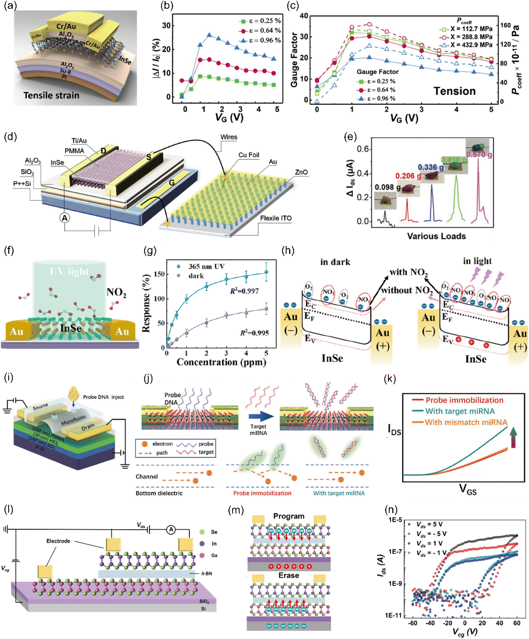 | ||
| Fig. 12 Advance sensor and memory on InSe nanoflakes. (a) Schematic of the three-dimensional structure of the device under an external tensile strain. (b) Ratio of current change (ΔI/I0) as a function of VG under various tensile strains. (c) Gauge factor and Pcoeff as a function of applied gate voltage (VG) under various tensile levels. Reproduced with permission.215 Copyright 2020, Elsevier. (d) Schematic diagram of ZnO NR arrays connected with the back-gate InSe-based FET. (e)ΔIds–load curves of different objects and the analyzed corresponding weights. Reproduced with permission.162 Copyright 2020, Elsevier. (f) Schematic of the NO2 gas sensor. (g) Response intensity curves of InSe/IDEs for 0.05–5 ppm of NO2 (n = 3). All operating temperatures are 30 °C, with a total gas flow rate of 1000 sccm; the background gas in all cases is air, except for the test of I–V curves, and all light intensities are 3.2 mW cm−2, unless noted otherwise. (h) Band diagram of the sensor depicting the interaction between InSe and NO2 molecules under two conditions. Reproduced with permission.165 Copyright 2020, American Chemical Society. (i) Structure of the InSe-FET biosensor. (j) Sensor mechanism of miRNA. (k) Drain current IDS response to complementary targets. Reproduced with permission.166 Copyright 2023, Wiley-VCH. (l) Schematic of the InSe/h-BN/GaSe floating-gate memory configuration. (m) Charge state of the device with gate voltage applied during the program and erase process. (n) Transfer curve (Ids–Vcg) of the InSe/h-BN/GaSe FG-FET for Vcg = ±60 V. Reproduced with permission.219 Copyright 2023, The Royal Society of Chemistry. | ||
In addition to the strain sensor, Wang et al.162 proposed a piezoelectric pressure sensor integrating flexible ZnO nanorod arrays with an InSe-based 2D FET. The schematic depiction of this setup is shown in Fig. 12(d); the ZnO nanorod arrays and InSe transistor are seamlessly connected by a metal conductor. These ZnO nanorod arrays exhibit rapid and sensitive response to pressure change, transforming mechanical stress into piezoelectric potential. This piezoelectric potential is applied to modulate the gate of the InSe-based FET, inducing a noticeable alteration in the drain–source current (Ids). Therefore, the magnitude of piezoelectric potential can be directly examined by the corresponding ΔIds, with a linear relationship between ΔIds and applied loadings over a wide range of 0.1–500 g. As shown in Fig. 12(e), the loadings of various samples were detected using the piezoelectric potential type pressure sensor, the results demonstrated consistent values with those obtained by a conventional electronic balance, indicating the high reliability and accuracy of the fabricated pressure sensor, which will facilitate broad application in mechanical stress detection.
Moreover, 2D InSe has shown considerable potential in the fabrication of gas sensors for harmful gases and greenhouse gases, such as NH3, NO2, and SO2. Lu et al.216 proved that a Ru modified InSe monolayer has potential application in the detection of harmful gases based on density functional theory. Zhang et al.165 fabricated a novel optoelectronic gas sensor based on InSe nanosheets shown in Fig. 12(f). NO2 can be detected at ambient temperature due to the excellent photoelectric and sensing properties of few-layer InSe. Furthermore, thanks to the excellent photosensitivity, gas-sensing properties and reversible responses were obtained under ultraviolet light illumination compared to those under dark conditions (Fig. 12(g)). In this InSe optoelectronic sensor, more active sites and sufficient photoexcited electrons are produced for NO2 adsorption and desorption under ultraviolet illumination. According to the mechanisms of NO2 detection as shown in Fig. 12(h), more NO2 can be adsorbed and electrons captured from the conduction band, and the Schottky barrier under ultraviolet light illumination is much higher than that under dark conditions. As a result, the fabricated sensor exhibits remarkable gas-sensing capability. This research not only broadens the application field of 2D InSe, but also demonstrates the potential prospect of detecting ppb-level NO2 under complex conditions even in human breath.
2D InSe-based FETs have the advantages of high speed, small size, low cost, and excellent compatibility with integrated circuits. Recently, InSe-based biosensors have been proposed for the detection of nucleic acids in viruses and early screening of critical diseases.156,166,217 Ji et al.166 reported an InSe-FET biosensor, to detect biomarker miRNAs in clinical serum samples and specific RNA in SARS-CoV-2 pseudo virus samples. The structure is shown in Fig. 12(i). Due to their small electron mass, carriers in InSe are extremely sensitive to surface impurity scattering. The mechanism during detection is shown in Fig. 12(j), where Coulomb scattering is the dominant sensing mechanism for carrier scattering-sensitive InSe. As a result, the back-gate bias working mode of the InSe-based FET biosensor possesses a linear relationship with an extra-large detectable range of 1 fM–10 nM. It demonstrated high specificity for identifying 1-nucleotide polymorphisms as well as excellent repeatability and reusability. In addition, Ji et al.217 proposed a high performance InSe biosensor for the detection of the breast cancer CA125 biomarker in clinical samples. 3-Aminopropyltriethoxysilane (APTES) as a coupling agent is functionalized on the InSe surface and the antibody CA125 is immobilized before biomarker detection. Once the target sample is loaded into the microfluidic channel, a positive shift in threshold voltage is induced by the antigen CA125 bonding with the antibody CA125, and is associated with antigen CA125 concentration. This biosensor achieved ultrasensitive, specific, fast, and label-free detection of the breast cancer biomarker CA125. These results indicate that 2D InSe can be useful for the early diagnosis of cancer, virus detection and the real-time monitoring of health.
2D materials represent an ideal atomically flat in-plane surface and are immune to short-channel effects, allowing effective electrostatic control. These unique features provide new applications in memory.167 Non-volatile memory devices have manifested high capacity and mechanical reliability. Wu et al.218 demonstrated an ultrahigh-speed non-volatile memory device based on InSe/h-BN/multilayer graphene van der Waals heterostructures as shown in Fig. 12(l). InSe, h-BN and multilayer graphene serve as the channel, tunnel barrier and floating gate, respectively. The ‘program state’ and ‘erase state’ were achieved when applying a positive voltage pulse and a negative voltage pulse to the control gate (Fig. 12(m)). This memory exhibited ultrahigh-speed operation of 21 ns. Coincidentally, Gong et al.219 reported tunable non-volatile memories based on 2D InSe/h-BN/GaSe heterostructures. InSe, h-BN and GaSe serve as the active channel, insulating layer and floating gate layer. The storage performance can be regulated by optimizing the thickness of the insulating h-BN layer, the tunneling barrier is reduced when decreasing the thickness of h-BN from 23 nm to 7 nm. The device shows good storage performance, such as a large on/off ratio of ∼105 and maximum storage capacity of 5.1 × 1012 cm−2. All these together offer the ground work for 2D memory and expand the exploration of next-generation electronic devices.
5 Outlook and future scope
In this review, we have discussed the recent advances in the process of InSe fabrication and applications in various domains, especially in FETs and photodetectors. This review paves the way for future studies on optimizing the mechanisms involved in InSe-based electronic and optoelectronic devices. Furthermore, the insights provided by this review presenting the optimization strategy of FETs and photodetectors can significantly enhance readers' comprehension of carrier transport. The strategies of synthesis, selection of the substrate and electrode materials, surface encapsulation and modification, as well as stacking techniques emerge as the pivotal factor to realize the desired characteristics.In short, the characteristics of electronic and optoelectronic devices are mainly determined by the properties of semiconductor materials and device construction techniques, which collectively influence signal output and device performance. The influence of the semiconductor material primarily hinges on its physicochemical properties, crystal quality and eventual presence of defects. Conversely, the device construction process is determined by heterogeneous interface properties such as the surface state of the semiconductor, the electrode material and the quality of the contact interface between the semiconductor and electrode material. Crucial phenomena and mechanisms, such as Fermi level pinning, carrier scattering, as well as physical and chemical adsorption, are not fully under the control of scientists due to the instability of the crystal quality and performance of semiconductor materials. Thus, a device with controllable performance cannot be achieved by optimizing the device preparation process alone. Simultaneously, in many instances the performance of the device does not accurately reflect the crystal quality and defect level of InSe due to the immature construction process, which cannot provide valuable guidance and instruction for material preparation and performance optimization. Therefore, the properties of semiconductor materials and device structure are interrelated and mutually affect each other. Considering the important features and current research status of InSe materials and devices, here we present our views on the remaining challenges, possibilities and outlook of future direction. Future research should focus on three aspects: the preparation of high-quality InSe crystal materials, control of the defect level, and control of the heterogeneous interface during device construction.
5.1 Controllable preparation of high quality InSe crystals
In the previous section, we have navigated the recent advances in two-dimensional InSe materials for electronic and optoelectronic applications. The physical properties and preparation methods were described briefly. The preparation methods can be divided into two principal types: the top-down exfoliation method and the bottom-up direct growth method. The former is based on bulk crystals prepared by the vapor phase transport method or melt method. The typical exfoliation methods used to prepare 2D materials are mechanical exfoliation and liquid phase exfoliation. The latter mainly involves chemical synthesis methods and physical synthesis methods, such as chemical vapor deposition, physical vapor deposition and other methods.The top-down exfoliation method is widely used for research of basic physical properties and preliminary exploration of two-dimensional materials; the mechanical exfoliation method can inherit the excellent crystallization quality of the bulk single crystal. However, the production of high-quality InSe single crystals remains challenging. InSe single crystals can be obtained by a peritectic reaction or from an In-rich melt; the excess indium accumulates at the front of the solid–liquid interface, which leads to local supercooling of the components and instability of the solid–liquid interface when InSe crystals are prepared by the melt method. Therefore, inclusions and small grain size often occur due to incomplete peritectic reaction during the growth of InSe. Simultaneously, issues such as crystal quality deterioration, diminished single crystal yield and impurity phase may appear due to deviations in stoichiometric ratio. To circumvent such challenges, it is pivotal to ensure the appropriate temperature gradient in the liquid phase and the liquid–solid interface during InSe crystal growth to avoid supercooling of the components. In addition, the inherent volatility of selenium element and the reactivity of indium element must be considered in the preparation of InSe crystals. The vapor pressure of selenium is higher at elevated temperature, which easily leads to the loss of selenium element in the melt resulting in deviation of the crystal composition from the stoichiometric ratio. Indium, a member of the IIIA group, showcases high chemical activity and easily forms an oxide layer In2O3 on the surface. In2O3 has a higher melting point and serves as a heterogeneous nucleation center during crystal growth, decreasing single crystal yield. Furthermore, indium has a tendency to react with the quartz crucible at high temperatures, and the excess indium causes adhesion between the InSe crystal ingot and the quartz crucible, affecting the integrity of the crystal ingot. Therefore, during crystal growth, the effects of various variables such as composition ratio, temperature gradient, growth rate, crucible material, and raw material purity should be comprehensively considered to obtain high-quality single crystals.
In the vapor phase deposition method of synthesis of 2D materials, there are several key challenges such as low growth rates, small grain sizes and uncontrollable thickness. Most vapor phase deposition processes are essentially surface processes which are easily affected by the substrate surface and interfacial activity of the gas and solid. In addition to the structure and orientation of the crystal plane, the surface activity of the solid-phase component also depends on the variety of impurities in the adsorption layer and the defect concentration in the near-surface layer. The polarity of the substrates dictates the amount of impurities adsorbed from the gaseous phase, while the nature of atoms and the arrangement of steps on the substrate crystal planes affect the nucleation and evolution of 2D materials. Furthermore, solid raw materials are inherently less controllable since the different reaction precursors normally have discrepant thermal properties. The discrepant thermal properties of source materials may result in asynchronous sublimation of precursors, deviation from the atomic molar ratio, inhomogeneous elemental distribution and even phase segregation may appear in the products. Therefore, the volatility of precursors, the flow and the temperature field require accurate calculation to avoid a mixed phase in the products, such as In2Se3 and In6Se7. Thus, a precisely controlled growth process and custom designed equipment are crucial factors for large-scale uniformity. It is very important to select the appropriate substrate materials and the appropriate crystal growth parameters when synthesizing two-dimensional InSe materials by vapor phase methods.
5.2 Precise control of defect level in InSe materials
In InSe materials, the primary intrinsic defect encompasses Se vacancy (VSe) and In interstitial atoms.220 Among these, the vacancy defect of chalcogenides is one of the most pivotal intrinsic defects in layered metal chalcogenides and has a significant influence on the electrical properties.221,222 Specifically, the Se vacancy is a deep level capture center that greatly affects charge carrier transport performance. In contrast, the In interstitial atom is a shallow level defect that plays a key role in the photoelectric conversion properties. Generally, the most intrinsic InSe crystals are n-type semiconductors. Moreover, stress can readily occur around vacancies in InSe, which significantly affect the mechanical properties of the material.223 As the vapor pressure of Se gradually increases at elevated temperatures, there is a resultant loss of Se element during the raw material reaction and crystal growth. This leads to the formation of numerous point defects and a deviation from the stoichiometric ratio. However, there are still few studies on the intrinsic defects of InSe (such as Se vacancies and In interstitials) and there remains a dearth of in-depth studies on their presence and reaction mechanisms, which cannot provide effective guidance for the design of crystal growth and performance regulation.Controllable doping with chemical elements is a pivotal strategy in semiconductor manufacturing to precisely regulate the transport and photoelectric properties of semiconductor materials. Two predominant doping techniques in practice are melt method doping and gas phase doping. In the realm of gas-phase doping, the distribution of dopants is related to the growth mechanism of adsorption of active units on the substrate surface and the inherent characteristics of the crystal. It has a tendency to have an uneven distribution, making it difficult to achieve consistent doping over expansive areas. Conversely, the melt method can provide a high-purity growth environment and accurate control of the stoichiometric ratio, but there are certain challenges in the uniform distribution of the dopant due to the segregation of the dopant and the limitation of the peritectic reaction. As a forward-looking recommendation, the reaction mechanism of the dopant, the doping efficiency, the occupied position in the lattice and the energy level of the dopant in the InSe crystal should be in-depth explored in the future.
5.3 Structure design and architecture process optimization of the InSe device
Through a comprehensive comparison of the performance of InSe two-dimensional electronic and optoelectronic devices with different structures, several key determinants that mainly influence the performance of InSe devices and preliminary conclusions can be identified. First, the interface both in the metal/2D material contact and the dielectric/2D materials plays a crucial role in the performance of FETs (Table 4 and Fig. 11(a)). Second, surface modification or doping in 2D materials significantly enhances the mobility of InSe transistors. It can not only screen the potential of charge impurities but also facilitate the formation of ohmic contact. Third, the very design and structure of devices, particularly the metal–semiconductor interface and the stacked heterostructure, have pronounced implications for their performance. It's evident that the performance of electronic and optoelectronic devices results from multifactorial coupling. It can be attributed to the combination of underneath physical and chemical effects at various heterogeneous interfaces, these encompass the following. (1) The scattering mechanism of carrier transport at the heterogeneous interface. In addition to the scattering at the interface of dielectric/2D materials, surface defects in the InSe material, impurities adsorbed on the surface of the dielectric material and the generated dangling bonds can interact to form a defect complex. This defect complex creates an additional defect trap level in the system and reduces device transport performance. (2) Scattering and charge doping of InSe surface defects. Due to the ultrathin thicknesses and large surface areas, two-dimensional semiconductor materials are vulnerable to environmental factors. The surface easily reacts with moisture and oxygen in the environment resulting in physical or chemical adsorption. Physical adsorption leads to strong scattering of carriers, while chemical adsorption can induce a doping effect of the surface charge. To avoid these problems, chemical functional group modification or surface encapsulation layer deposition has been applied to achieve surface doping or passivation of channel materials during device preparation. (3) Contact barrier and the Fermi level pinning mechanism of metal/semiconductor interface and band alignment of the two-dimensional heterostructure. Metal/2D material contact without optimal treatment can lead to several factors such as metal induced gap state, surface adsorbates and defects, these can cause Fermi level pinning and a high Schottky barrier height. Both the intrinsic defects of InSe crystals and surface damage generated during device fabrication contribute to the Fermi level pinning at the metal/semiconductor interface. It has a direct impact on carrier collection, resulting in a discrepancy between anticipated and observed device performance. 2D heterostructures achieved numerous electronic and optoelectronic characteristics due to the appropriate band alignment, such as ohmic contact, large optical absorption, and high interlayer excitation. Usually, stacking and direct synthesis methods are utilized for the fabrication of the vdW heterostructures. But they suffer from low yields, possessing defects, etc., which limit them from achieving theoretical performance. In the future, a profound comprehension is urgently needed of the physical and chemical mechanism at heterogeneous interfaces based on InSe materials with intrinsic defects. Furthermore, there are critical problems that need to be focused during the process of device construction and design. For instance, novel device design with unique physical phenomena can be investigated via stacking of dielectric, metallic, and 2D semiconductors, while taking into account and balancing the main factors affecting the performance of the device to prepare high-performance devices.6 Summary
In conclusion, numerous research studies have explored 2D InSe in recent years in the perspective of its physical properties, fabrication and synthesis strategies as well as advanced device applications, which present great opportunities and challenges. As one of the most promising semiconductor materials for electronic and optoelectronic devices, the intrinsic defects of two-dimensional InSe not only affect the material physical properties such as carrier transport, but also cause severe surface and interface problems, which are the main factors for the unstable performance of InSe devices. It is essential to understand the fundamental relationship between the precise control of material defects and multifactorial coupling mechanism that affect the properties of InSe devices. It is critical to look into new methods or enhance the existing ones for InSe crystal growth and large-scale synthesis techniques, precise control of defects and dopants, and appropriate stacking techniques in surface and heterogeneous interfaces. Achieving stable and reliable high-performance applications in the field of optoelectronic devices, as well as other advanced applications such as flexible sensors and wearable/portable electronic devices, will be crucial in the future.Author contributions
Dan Zheng and Peng Chen participated in the investigation and writing of the original draft for InSe fundamental properties, two-dimensional InSe material fabrication and synthesis techniques, and InSe advanced device application. Yi Liu, Xing Li, and Kejing Liu participated in the investigation and writing of the original draft for the Outlook and future scope and Summary. Zi'ang Yin and Riccardo Frisenda participated in the revision and editing of this manuscript. Qinghua Zhao and Tao Wang made substantial contributions to the conception and design of this manuscript, and gave the final approval.Conflicts of interest
The authors declare no competing interests.Acknowledgements
This work was supported by the Guangdong Basic and Applied Basic Research Foundation (Grant No. 2022A1515110538); Shenzhen Science and Technology Program 2022-47; Key Research and Development Program of Shaanxi (Program No. 2022GY-354); the National Natural Science Foundation of China (52072300, 52302199); the Research Fund of the State Key Laboratory of Solidification Processing (NPU), China (Grant No. 2022-QZ-01), Fundamental Research Funds for Central Universities (D5000220053), Shccig-Qinling Program and the Key Research and Development Program of Shaanxi (Program No. 2023-GHZD-48).References
- M. M. Waldrop, Nature, 2016, 530, 144 CrossRef CAS PubMed.
- Y. Liu, X. Duan, H.-J. Shin, S. Park, Y. Huang and X. Duan, Nature, 2021, 591, 43–53 CrossRef CAS PubMed.
- C. Liu, H. Chen, S. Wang, Q. Liu, Y. G. Jiang, D. W. Zhang, M. Liu and P. Zhou, Nat. Nanotechnol., 2020, 15, 545–557 CrossRef CAS PubMed.
- M. J. Allen, V. C. Tung and R. B. Kaner, Chem. Rev., 2010, 110, 132–145 CrossRef CAS PubMed.
- M. Chhowalla, D. Jena and H. Zhang, Nat. Rev. Mater., 2016, 1, 16052 CrossRef CAS.
- University of Manchester, in Phys.org, 2016, https://phys.org/news/2016-11-ultra-thin-semiconductor-life-law.html.
- R. W. Damon and R. W. Redington, Phys. Rev., 1954, 96, 1498–1500 CrossRef CAS.
- K. Schubert, E. Dörre and E. Günzel, Naturwissenschaften, 1954, 41, 448 CrossRef CAS.
- T. Ikari, S. Shigetomi and K. Hashimoto, Phys. Status Solidi B, 1982, 111, 477–481 CrossRef CAS.
- G. Han, Z. G. Chen, J. Drennan and J. Zou, Small, 2014, 10, 2747–2765 CrossRef CAS PubMed.
- S. Lei, L. Ge, S. Najmaei, A. George, R. Kappera, J. Lou, M. Chhowalla, H. Yamaguchi, G. Gupta and R. Vajtai, ACS Nano, 2014, 8, 1263–1272 CrossRef CAS PubMed.
- B. Gürbulak, M. Şata, S. Dogan, S. Duman, A. Ashkhasi and E. F. Keskenler, Phys. E: Low-Dimens. Syst. Nanostructures., 2014, 64, 106–111 CrossRef.
- Q. Hao, H. Yi, H. Su, B. Wei, Z. Wang, Z. Lao, Y. Chai, Z. Wang, C. Jin, J. Dai and W. Zhang, Nano Lett., 2019, 19, 2634–2640 CrossRef CAS PubMed.
- I. Grimaldi, T. Gerace, M. M. Pipita, I. D. Perrotta, F. Ciuchi, H. Berger, M. Papagno, M. Castriota and D. Pacilé, Solid State Commun., 2020, 311, 113855 CrossRef CAS.
- M. Dai, H. Chen, F. Wang, Y. Hu, S. Wei, J. Zhang, Z. Wang, T. Zhai and P. Hu, ACS Nano, 2019, 13, 7291–7299 CrossRef CAS PubMed.
- H. Hu, Y. Sun, M. Chai, D. Xie, J. Ma and H. Zhu, Appl. Phys. Lett., 2019, 114, 252903 CrossRef.
- F. Sui, M. Jin, Y. Zhang, R. Qi, Y.-N. Wu, R. Huang, F. Yue and J. Chu, Nat. Commun., 2023, 14, 36 CrossRef CAS PubMed.
- M. Osman, Y. Huang, W. Feng, G. Liu, Y. Qiu and P. Hu, RSC Adv., 2016, 6, 70452–70459 RSC.
- H. Su, X. Liu, C. Wei, J. Li, Z. Sun, Q. Liu, X. Zhou, J. Deng, H. Yi, Q. Hao, Y. Zhao, S. Wang, L. Huang, S. Wu, W. Zhang, G. Li and J.-F. Dai, Laser Photonics Rev., 2019, 13, 1900012 CrossRef.
- S. Liu, Y. Yang, F. Yu, X. Wen, Z. Gui, K. Peng, R. Wang and J. Ying, Phys. Rev. B, 2022, 105, 214506 CrossRef CAS.
- X. Cheng, Z. Huangfu, H. Zhang, J. Wang, S. Feng, Y. Liang, X. Zhu, Z. Wang, X. Wu and K. Yang, J. Alloys Compd., 2024, 970, 172636 CrossRef CAS.
- D. Errandonea, D. Martínez-García, A. Segura, A. Chevy, G. Tobias, E. Canadell and P. Ordejon, Phys. Rev. B: Condens. Matter Mater. Phys., 2006, 73, 235202 CrossRef.
- M. Wasala, H. I. Sirikumara, Y. Raj Sapkota, S. Hofer, D. Mazumdar, T. Jayasekera and S. Talapatra, J. Mater. Chem. C, 2017, 5, 11214–11225 RSC.
- Q. Zhao, S. Puebla, W. Zhang, T. Wang, R. Frisenda and A. Castellanos-Gomez, Adv. Photonics Res., 2020, 1, 2000025 CrossRef.
- L. Zhao, Y. Jiang, C. Li, Y. Liang, Z. Wei, X. Wei and Q. Zhang, Nano Lett., 2023, 23, 3493–3500 CrossRef CAS PubMed.
- K. S. Novoselov, A. K. Geim, S. V. Morozov, D. Jiang, Y. Zhang, S. V. Dubonos, I. V. Grigorieva and A. A. Firsov, Science, 2004, 306, 666–669 CrossRef CAS PubMed.
- F. Xia, H. Wang and Y. Jia, Nat. Commun., 2014, 5, 4458 CrossRef CAS PubMed.
- H. Li, J. Wu, Z. Yin and H. Zhang, Acc. Chem. Res., 2014, 47, 1067–1075 CrossRef CAS PubMed.
- E. Gao, S.-Z. Lin, Z. Qin, M. J. Buehler, X.-Q. Feng and Z. Xu, J. Mech. Phys. Solids, 2018, 115, 248–262 CrossRef CAS.
- M. Yi and Z. Shen, J. Mater. Chem. A, 2015, 3, 11700–11715 RSC.
- B. Zhang, H. Wu, K. Peng, X. Shen, X. Gong, S. Zheng, X. Lu, G. Wang and X. Zhou, Chin. Phys. B, 2021, 30, 078101 CrossRef CAS.
- R. Triboulet, C. Levy-Clement, B. Theys and A. Chevy, J. Cryst. Growth, 1986, 79, 984–989 CrossRef CAS.
- M. Jin, Y. Ma, T. Wei, X. Bai, Y. Peng, X. Chen, X. Xu, X. Liu and X. Shi, SSRN Electronic Journal, 2022, 4084618 Search PubMed.
- M. Sun, W. Wang, Q. Zhao, X. Gan, Y. Sun, W. Jie and T. Wang, Crystengcomm, 2020, 22, 7864–7869 RSC.
- M. Dai, C. Gao, Q. Nie, Q. J. Wang, Y. F. Lin, J. Chu and W. Li, Adv. Mater. Technol., 2022, 7, 2200321 CrossRef CAS.
- T. Venanzi, H. Arora, S. Winnerl, A. Pashkin, P. Chava, A. Patane, Z. D. Kovalyuk, Z. R. Kudrynskyi, K. Watanabe, T. Taniguchi, A. Erbe, M. Helm and H. Schneider, Phys. Rev. Mater., 2020, 4, 044001 CrossRef CAS.
- D. A. Bandurin, A. V. Tyurnina, G. L. Yu, A. Mishchenko, V. Zolyomi, S. V. Morozov, R. K. Kumar, R. V. Gorbachev, Z. R. Kudrynskyi, S. Pezzini, Z. D. Kovalyuk, U. Zeitler, K. S. Novoselov, A. Patane, L. Eaves, I. V. Grigorieva, V. I. Fal'ko, A. K. Geim and Y. Cao, Nat. Nanotechnol., 2017, 12, 223–227 CrossRef CAS PubMed.
- C. Huo, Z. Yan, X. Song and H. Zeng, Sci. Bull., 2015, 60, 1994–2008 CrossRef CAS.
- C. M. Nicolosi V and M. G. Kanatzidis, et al , Science, 2013, 340, 1226419 CrossRef.
- E. Petroni, E. Lago, S. Bellani, D. W. Boukhvalov, A. Politano, B. Gürbulak, S. Duman, M. Prato, S. Gentiluomo, R. Oropesa-Nuñez, J.-K. Panda, P. S. Toth, A. E. Del Rio Castillo, V. Pellegrini and F. Bonaccorso, Small, 2018, 14, 1800749 CrossRef PubMed.
- Z. Li, H. Qiao, Z. Guo, X. Ren, Z. Huang, X. Qi, S. C. Dhanabalan, J. S. Ponraj, D. Zhang, J. Li, J. Zhao, J. Zhong and H. Zhang, Adv. Funct. Mater., 2018, 28, 1705237 CrossRef.
- Y. Liao, Y. Shan, L. Wu, Y. Xiang and X. Dai, Adv. Opt. Mater., 2020, 8, 1901862 CrossRef CAS.
- J. Kang, S. A. Wells, V. K. Sangwan, D. Lam, X. Liu, L. Jan, Z. Sofer and M. C. Hersam, Adv. Mater., 2018, 30, 1802990 CrossRef PubMed.
- M. Brotons-Gisbert, J. F. Sánchez-Royo and J. P. Martínez-Pastor, Appl. Surf. Sci., 2015, 354, 453–458 CrossRef CAS.
- J. Zhang, F. Wang, V. B. Shenoy, M. Tang and J. Lou, Mater. Today, 2020, 40, 132–139 CrossRef CAS.
- J. Wang, T. Liang, H. Li, J. Xiong, B. Liu, X. Xu, Y. Gao, Z. Yu, Q. Zheng, S. Zhang and B. Wang, Chin. Chem. Lett., 2023, 34, 107826 CrossRef CAS.
- W. Huang, L. Gan, H. Li, Y. Ma and T. Zhai, Chem.–Eur. J., 2018, 24, 15678–15684 CrossRef CAS PubMed.
- H.-C. Chang, C.-L. Tu, K.-I. Lin, J. Pu, T. Takenobu, C.-N. Hsiao and C.-H. Chen, Small, 2018, 14, 1802351 CrossRef PubMed.
- C.-Y. Wu, K.-J. Cao, Y.-X. Le, J.-Y. Li, C.-Y. Zhu, L. Wang, Y.-X. Zhou, D. Wu and L.-B. Luo, J. Phys. Chem. Lett., 2022, 13, 2668–2673 CrossRef CAS PubMed.
- S. Song, S. Jeon, M. Rahaman, J. Lynch, D. Rhee, P. Kumar, S. Chakravarthi, G. Kim, X. Du, E. W. Blanton, K. Kisslinger, M. Snure, N. R. Glavin, E. A. Stach, R. H. Olsson Iii and D. Jariwala, Matter, 2023, 6, 3483–3498 CrossRef CAS.
- D. Wang, F. Luo, M. Lu, X. Xie, L. Huang and W. Huang, Small, 2019, 15, 1804404 CrossRef PubMed.
- J. Yao and G. Yang, Adv. Sci., 2022, 9, 2103036 CrossRef PubMed.
- J. Wang, H. Zheng, G. Xu, L. Sun, D. Hu, Z. Lu, L. Liu, J. Zheng, C. Tao and L. Jiao, J. Am. Chem. Soc., 2016, 138, 16216–16219 CrossRef CAS PubMed.
- K. Yuan, R. Yin, X. Li, Y. Han, M. Wu, S. Chen, S. Liu, X. Xu, K. Watanabe, T. Taniguchi, D. A. Muller, J. Shi, P. Gao, X. Wu, Y. Ye and L. Dai, Adv. Funct. Mater., 2019, 29, 1904032 CrossRef.
- L. A. Walsh and C. L. Hinkle, Appl. Mater. Today, 2017, 9, 504–515 CrossRef.
- X. Yuan, L. Tang, S. Liu, P. Wang, Z. Chen, C. Zhang, Y. Liu, W. Wang, Y. Zou, C. Liu, N. Guo, J. Zou, P. Zhou, W. Hu and F. Xiu, Nano Lett., 2015, 15, 3571–3577 CrossRef CAS PubMed.
- S. M. Poh, X. Zhao, S. J. R. Tan, D. Fu, W. Fei, L. Chu, D. Jiadong, W. Zhou, S. J. Pennycook, A. H. Castro Neto and K. P. Loh, ACS Nano, 2018, 12, 7562–7570 CrossRef CAS PubMed.
- S. V. Sorokin, P. S. Avdienko, I. V. Sedova, D. A. Kirilenko, M. A. Yagovkina, A. N. Smirnov, V. Y. Davydov and S. V. Ivanov, Semiconductors, 2019, 53, 1131–1137 CrossRef CAS.
- S. V. Sorokin, P. S. Avdienko, I. V. Sedova, D. A. Kirilenko, V. Y. Davydov, O. S. Komkov, D. D. Firsov and S. V. Ivanov, Materials, 2020, 13, 3447 CrossRef CAS PubMed.
- S. M. Poh, S. J. R. Tan, H. Wang, P. Song, I. H. Abidi, X. Zhao, J. Dan, J. Chen, Z. Luo, S. J. Pennycook, A. H. Castro Neto and K. P. Loh, Nano Lett., 2018, 18, 6340–6346 CrossRef CAS PubMed.
- W. Fu, X. Zhao, K. Wang, Z. Chen, K. Leng, D. Fu, P. Song, H. Wang, L. Deng, S. J. Pennycook, G. Zhang, B. Peng and K. P. Loh, Nano Lett., 2020, 20, 5330–5338 CrossRef CAS PubMed.
- Z. Zhang, Y. Yuan, W. Zhou, C. Chen, S. Yuan, H. Zeng, Y.-S. Fu and W. Zhang, ACS Nano, 2021, 15, 10700–10709 CrossRef CAS PubMed.
- D. S. H. Liu, M. Hilse, A. R. Lupini, J. M. Redwing and R. Engel-Herbert, ACS Appl. Nano Mater., 2023, 6, 15029 CrossRef CAS.
- K. Li, K. Ling, W. Li and X. Liu, IEEE Sens. J., 2023, 23, 30318–30324 CAS.
- M. S. Claro, J. P. Martínez-Pastor, A. Molina-Sánchez, K. E. Hajraoui, J. Grzonka, H. P. Adl, D. Fuertes Marrón, P. J. Ferreira, O. Bondarchuk and S. Sadewasser, Adv. Funct. Mater., 2023, 33, 2211871 CrossRef CAS.
- S. Hao, S. Yan, Y. Wang, T. Xu, H. Zhang, X. Cong, L. Li, X. Liu, T. Cao, A. Gao, L. Zhang, L. Jia, M. Long, W. Hu, X. Wang, P. Tan, L. Sun, X. Cui, S.-J. Liang and F. Miao, Small, 2020, 16, 1904032 CrossRef PubMed.
- J. Cai, X. Han, X. Wang and X. Meng, Matter, 2020, 2, 587–630 CrossRef.
- H. G. Kim and H.-B.-R. Lee, Chem. Mater., 2017, 29, 3809–3826 CrossRef CAS.
- A. Sharma, R. Mahlouji, L. Wu, M. A. Verheijen, V. Vandalon, S. Balasubramanyam, J. P. Hofmann, W. M. M. Kessels and A. A. Bol, Nanotechnology, 2020, 31, 255603 CrossRef CAS PubMed.
- S. M. George, Chem. Rev., 2010, 110, 111–131 CrossRef CAS PubMed.
- A. Sharma, M. A. Verheijen, L. Wu, S. Karwal, V. Vandalon, H. C. M. Knoops, R. S. Sundaram, J. P. Hofmann, W. M. M. Kessels and A. A. Bol, Nanoscale, 2018, 10, 8615–8627 RSC.
- R. Browning, N. Kuperman, B. Moon and R. Solanki, Electronics, 2017, 6, 27 CrossRef.
- Z. Lin, A. McCreary, N. Briggs, S. Subramanian, K. Zhang, Y. Sun, X. Li, N. J. Borys, H. Yuan, S. K. Fullerton-Shirey, A. Chernikov, H. Zhao, S. McDonnell, A. M. Lindenberg, K. Xiao, B. J. LeRoy, M. Drndić, J. C. M. Hwang, J. Park, M. Chhowalla, R. E. Schaak, A. Javey, M. C. Hersam, J. Robinson and M. Terrones, 2D Mater., 2016, 3, 042001 CrossRef.
- J. Ning, G. Xiao, N. Xiao, L. Wang, B. Liu and B. Zou, J. Cryst. Growth, 2011, 336, 1–5 CrossRef CAS.
- M. A. Airo, S. Gqoba, M. P. Kalenga, S. Govindraju, M. J. Moloto and N. Moloto, J. Cryst. Growth, 2014, 406, 1–7 CrossRef CAS.
- J. Lauth, F. E. S. Gorris, M. S. Khoshkhoo, T. Chasse, W. Friedrich, V. Lebedeya, A. Meyer, C. Klinke, A. Komowsld, M. Scheele and H. Weller, Chem. Mater., 2016, 28, 1728–1736 CrossRef CAS.
- G. Karmakar, D. D. Pathak, A. Tyagi, B. P. Mandal, A. P. Wadawale and G. Kedarnath, Dalton Trans., 2023, 52, 6700–6711 RSC.
- R. Dong, T. Zhang and X. Feng, Chem. Rev., 2018, 118, 6189–6235 CrossRef CAS PubMed.
- J. Zhou, J. Shi, Q. Zeng, Y. Chen, L. Niu, F. Liu, T. Yu, K. Suenaga, X. Liu, J. Lin and Z. Liu, 2D Mater., 2018, 5, 025019 CrossRef.
- N. Balakrishnan, E. D. Steer, E. F. Smith, Z. R. Kudrynskyi, Z. D. Kovalyuk, L. Eaves, A. Patane and P. H. Beton, 2D Mater., 2018, 5, 035026 CrossRef.
- Z. Yang, W. Jie, C.-H. Mak, S. Lin, H. Lin, X. Yang, F. Yan, S. P. Lau and J. Hao, ACS Nano, 2017, 11, 4225–4236 CrossRef CAS PubMed.
- J. D. Yao, Z. Q. Zheng and G. W. Yang, Prog. Mater. Sci., 2019, 106, 100573 CrossRef CAS.
- J. Hao, Y. Zhang and X. Wei, Angew. Chem., Int. Ed., 2011, 50, 6876–6880 CrossRef CAS PubMed.
- T. Liu, C. Han, D. Xiang, K. Han, A. Ariando and W. Chen, Adv. Sci., 2020, 7, 2002393 CrossRef CAS PubMed.
- R. Svoboda, L. Durcikova, J. Prikryl, K. Hamano, P. J. Fons and M. Krbal, J. Phys. Chem. C, 2023, 127, 16132–16147 CrossRef CAS.
- V. J. C. Rigi, M. K. Jayaraj and K. J. Saji, Appl. Surf. Sci., 2020, 529, 147158 CrossRef CAS.
- C. Muratore, A. A. Voevodin and N. R. Glavin, Thin Solid Films, 2019, 688, 137500 CrossRef CAS.
- X. Yan, X. Wu, Y. Fang, W. Sun, C. Yao, Y. Wang, X. Zhang and Y. Song, RSC Adv., 2020, 10, 2959–2966 RSC.
- H.-W. Yang, H.-F. Hsieh, R.-S. Chen, C.-H. Ho, K.-Y. Lee and L.-C. Chao, ACS Appl. Mater. Interfaces, 2018, 10, 5740–5749 CrossRef CAS PubMed.
- W. Feng, W. Zheng, W. Cao and P. Hu, Adv. Mater., 2014, 26, 6587–6593 CrossRef CAS PubMed.
- H. Bergeron, L. M. Guiney, M. E. Beck, C. Zhang, V. K. Sangwan, C. G. Torres-Castanedo, J. T. Gish, R. Rao, D. R. Austin, S. Guo, D. Lam, K. Su, P. T. Brown, N. R. Glavin, B. Maruyama, M. J. Bedzyk, V. P. Dravid and M. C. Hersam, Appl. Phys. Rev., 2020, 7, 041402 CAS.
- S. Poncé, W. Li, S. Reichardt and F. Giustino, Rep. Prog. Phys., 2020, 83, 036501 CrossRef PubMed.
- W. Feng, W. Zheng, F. Gao and P. Hu, Sci. China: Technol. Sci., 2017, 60, 1121–1122 CrossRef CAS.
- Y. Yoon, K. Ganapathi and S. Salahuddin, Nano Lett., 2011, 11, 3768–3773 CrossRef CAS PubMed.
- W. Feng, X. Zhou, W. Q. Tian, W. Zheng and P. Hu, Phys. Chem. Chem. Phys., 2015, 17, 3653–3658 RSC.
- R.-S. Chen, C.-C. Tang, W.-C. Shen and Y.-S. Huang, Nanotechnology, 2014, 25, 415706 CrossRef PubMed.
- G. W. Mudd, S. A. Svatek, T. Ren, A. Patane, O. Makarovsky, L. Eaves, P. H. Beton, Z. D. Kovalyuk, G. V. Lashkarev, Z. R. Kudrynskyi and A. I. Dmitriev, Adv. Mater., 2013, 25, 5714–5718 CrossRef CAS PubMed.
- G. W. Mudd, M. R. Molas, X. Chen, V. Zólyomi, K. Nogajewski, Z. R. Kudrynskyi, Z. D. Kovalyuk, G. Yusa, O. Makarovsky, L. Eaves, M. Potemski, V. I. Fal’ko and A. Patanè, Sci. Rep., 2016, 6, 39619 CrossRef CAS PubMed.
- L. Li, Y. Yu, G. J. Ye, Q. Ge, X. Ou, H. Wu, D. Feng, X. H. Chen and Y. Zhang, Nat. Nanotechnol., 2014, 9, 372–377 CrossRef CAS PubMed.
- V. Tran, R. Soklaski, Y. Liang and L. Yang, Phys. Rev. B: Condens. Matter Mater. Phys., 2014, 89, 235319 CrossRef.
- J. Qiao, X. Kong, Z.-X. Hu, F. Yang and W. Ji, Nat. Commun., 2014, 5, 4475 CrossRef CAS PubMed.
- K. F. Mak, C. Lee, J. Hone, J. Shan and T. F. Heinz, Phys. Rev. Lett., 2010, 105, 136805 CrossRef PubMed.
- B. Radisavljevic and A. Kis, Nat. Mater., 2013, 12, 815–820 CrossRef CAS PubMed.
- Y. Zhang, T.-R. Chang, B. Zhou, Y.-T. Cui, H. Yan, Z. Liu, F. Schmitt, J. Lee, R. Moore, Y. Chen, H. Lin, H.-T. Jeng, S.-K. Mo, Z. Hussain, A. Bansil and Z.-X. Shen, Nat. Nanotechnol., 2014, 9, 111–115 CrossRef CAS PubMed.
- S.-L. Li, K. Tsukagoshi, E. Orgiu and P. Samorì, Chem. Soc. Rev., 2016, 45, 118–151 RSC.
- S. Larentis, B. Fallahazad and E. Tutuc, Appl. Phys. Lett., 2012, 101, 223104 CrossRef.
- J. Gusakova, X. Wang, L. L. Shiau, A. Krivosheeva, V. Shaposhnikov, V. Borisenko, V. Gusakov and B. K. Tay, Phys. Status Solidi A, 2017, 214, 1700218 CrossRef.
- H. Fang, S. Chuang, T. C. Chang, K. Takei, T. Takahashi and A. Javey, Nano Lett., 2012, 12, 3788–3792 CrossRef CAS PubMed.
- H.-J. Chuang, B. Chamlagain, M. Koehler, M. M. Perera, J. Yan, D. Mandrus, D. Tománek and Z. Zhou, Nano Lett., 2016, 16, 1896–1902 CrossRef CAS PubMed.
- W. Zhao, Z. Ghorannevis, L. Chu, M. Toh, C. Kloc, P.-H. Tan and G. Eda, ACS Nano, 2013, 7, 791–797 CrossRef CAS PubMed.
- B. W. H. Baugher, H. O. H. Churchill, Y. Yang and P. Jarillo-Herrero, Nat. Nanotechnol., 2014, 9, 262–267 CrossRef CAS PubMed.
- Z. Jin, X. Li, J. T. Mullen and K. W. Kim, Phys. Rev. B: Condens. Matter Mater. Phys., 2014, 90, 045422 CrossRef CAS.
- S. Tongay, W. Fan, J. Kang, J. Park, U. Koldemir, J. Suh, D. S. Narang, K. Liu, J. Ji, J. Li, R. Sinclair and J. Wu, Nano Lett., 2014, 14, 3185–3190 CrossRef CAS PubMed.
- A. L. Elías, N. Perea-López, A. Castro-Beltrán, A. Berkdemir, R. Lv, S. Feng, A. D. Long, T. Hayashi, Y. A. Kim, M. Endo, H. R. Gutiérrez, N. R. Pradhan, L. Balicas, T. E. Mallouk, F. López-Urías, H. Terrones and M. Terrones, ACS Nano, 2013, 7, 5235–5242 CrossRef PubMed.
- D. Ovchinnikov, A. Allain, Y.-S. Huang, D. Dumcenco and A. Kis, ACS Nano, 2014, 8, 8174–8181 CrossRef CAS PubMed.
- Q. Zhao, W. Wang, F. Carrascoso-Plana, W. Jie, T. Wang, A. Castellanos-Gomez and R. Frisenda, Mater. Horiz., 2020, 7, 252–262 RSC.
- Y. Wang, H. Wang, S. M. Gali, N. Turetta, Y. Yao, C. Wang, Y. Chen, D. Beljonne and P. Samorì, Adv. Funct. Mater., 2021, 31, 2103353 CrossRef CAS.
- J. Jiang, J. Li, Y. Li, J. Duan, L. Li, Y. Tian, Z. Zong, H. Zheng, X. Feng, Q. Li, H. Liu, Y. Zhang, T.-L. Ren and L. Han, npj 2D Mater. Appl., 2019, 3, 29 CrossRef.
- S. Sucharitakul, N. J. Goble, U. R. Kumar, R. Sankar, Z. A. Bogorad, F.-C. Chou, Y.-T. Chen and X. P. A. Gao, Nano Lett., 2015, 15, 3815–3819 CrossRef CAS PubMed.
- S.-L. Li, K. Wakabayashi, Y. Xu, S. Nakaharai, K. Komatsu, W.-W. Li, Y.-F. Lin, A. Aparecido-Ferreira and K. Tsukagoshi, Nano Lett., 2013, 13, 3546–3552 CrossRef CAS PubMed.
- S. Zhang, Y. Qiu, H. Yang, D. Wang, Y. Hu, X. Lu, Z. Li and P. Hu, J. Mater. Chem. C, 2020, 8, 6701–6709 RSC.
- Y. Zhao, K. Xu, F. Pan, C. Zhou, F. Zhou and Y. Chai, Adv. Funct. Mater., 2017, 27, 1603484 CrossRef.
- J. Zeng, S.-J. Liang, A. Gao, Y. Wang, C. Pan, C. Wu, E. Liu, L. Zhang, T. Cao, X. Liu, Y. Fu, Y. Wang, K. Watanabe, T. Taniguchi, H. Lu and F. Miao, Phys. Rev. B, 2018, 98, 125414 CrossRef CAS.
- C. R. Dean, A. F. Young, I. Meric, C. Lee, L. Wang, S. Sorgenfrei, K. Watanabe, T. Taniguchi, P. Kim, K. L. Shepard and J. Hone, Nat. Nanotechnol., 2010, 5, 722–726 CrossRef CAS PubMed.
- Z. Liu, Y. Gong, W. Zhou, L. Ma, J. Yu, J. C. Idrobo, J. Jung, A. H. Macdonald, R. Vajtai, J. Lou and P. M. Ajayan, Nat. Commun., 2013, 4, 2541 CrossRef PubMed.
- Y. H. Chen, C. Y. Cheng, S. Y. Chen, J. S. D. Rodriguez, H. T. Liao, K. Watanabe, T. Taniguchi, C. W. Chen, R. Sankar, F. C. Chou, H. C. Chiu and W. H. Wang, npj 2D Mater. Appl., 2019, 3, 49 CrossRef CAS.
- H. Arora, Y. Jung, T. Venanzi, K. Watanabe, T. Taniguchi, R. Huebner, H. Schneider, M. Helm, J. C. Hone and A. Erbe, ACS Appl. Mater. Interfaces, 2019, 11, 43480–43487 CrossRef CAS PubMed.
- P.-H. Ho, Y.-R. Chang, Y. C. Chu, M. K. Li, C. A. Tsai, W. H. Wang, C. H. Ho, C. W. Chen and P. W. Chiu, ACS Nano, 2017, 11, 7362–7370 CrossRef CAS PubMed.
- T. H. Tsai, F. S. Yang, P. H. Ho, Z. Y. Liang, C. H. Lien, C. H. Ho, Y. F. Lin and P. W. Chiu, ACS Appl. Mater. Interfaces, 2019, 11, 35969–35976 CrossRef CAS PubMed.
- F. Leonard and A. A. Talin, Nat. Nanotechnol., 2011, 6, 773–783 CrossRef CAS PubMed.
- B. Shi, Y. Wang, J. Li, X. Zhang, J. Yan, S. Liu, J. Yang, Y. Pan, H. Zhang, J. Yang, F. Pan and J. Lu, Phys. Chem. Chem. Phys., 2018, 20, 24641–24651 RSC.
- Y. T. Huang, Y. H. Chen, Y. J. Ho, S. W. Huang, Y. R. Chang, K. Watanabe, T. Taniguchi, H. C. Chiu, C. T. Liang, R. Sankar, F. C. Chou, C. W. Chen and W. H. Wang, ACS Appl. Mater. Interfaces, 2018, 10, 33450–33456 CrossRef CAS PubMed.
- Z. Li, J. Liu, H. Ou, Y. Hu, J. Zhu, J. Huang, H. Liu, Y. Tu, D. Qi, Q. Hao and W. Zhang, Nanomaterials, 2024, 14, 382 CrossRef CAS PubMed.
- M. Li, C. Y. Lin, S. H. Yang, Y. M. Chang, J. K. Chang, F. S. Yang, C. Zhong, W. B. Jian, C. H. Lien, C. H. Ho, H. J. Liu, R. Huang, W. Li, Y. F. Lin and J. Chu, Adv. Mater., 2018, 30, 1803690 CrossRef PubMed.
- J. Jiang, L. Xu, C. Qiu and L.-M. Peng, Nature, 2023, 616, 470–475 CrossRef CAS PubMed.
- T. Y. Liow, K. M. Tan, H. C. Chin, R. T. P. Lee, C. H. Tung, G. S. Samudra, N. Balasubramanian and Y.-C. Yeo, International Electron Devices Meeting, 2006, pp. 1–4 Search PubMed.
- V. Barral, T. Poiroux, M. Vinet, J. Widiez, B. Previtali, P. Grosgeorges, G. Le Carval, S. Barraud, J. L. Autran, D. Munteanu and S. Deleonibus, Solid-State Electron., 2007, 51, 537–542 CrossRef CAS.
- M. Li, C. Y. Lin, S. H. Yang, Y. M. Chang, J. K. Chang, F. S. Yang, C. Zhong, W. B. Jian, C. H. Lien, C. H. Ho, H. J. Liu, R. Huang, W. Li, Y. F. Lin and J. Chu, Adv. Mater., 2018, 30, 1803690 CrossRef PubMed.
- L. Wu, J. Shi, Z. Zhou, J. Yan, A. Wang, C. Bian, J. Ma, R. Ma, H. Liu, J. Chen, Y. Huang, W. Zhou, L. Bao, M. Ouyang, S. T. Pantelides and H.-J. Gao, Nano Res., 2020, 13, 1127–1132 CrossRef CAS.
- W. Feng, W. Zheng, X. Chen, G. Liu and P. Hu, ACS Appl. Mater. Interfaces, 2015, 7, 26691–26695 CrossRef CAS PubMed.
- S. A. Wells, A. Henning, J. T. Gish, V. K. Sangwan, L. J. Lauhon and M. C. Hersam, Nano Lett., 2018, 18, 7876–7882 CrossRef CAS PubMed.
- W. Feng, J.-B. Wu, X. Li, W. Zheng, X. Zhou, K. Xiao, W. Cao, B. Yang, J.-C. Idrobo, L. Basile, W. Tian, P. Tan and P. Hu, J. Mater. Chem. C, 2015, 3, 7022–7028 RSC.
- J. Jiang, J. Li, Y. Li, J. Duan, L. Li, Y. Tian, Z. Zong, H. Zheng, X. Feng, Q. Li, H. Liu, Y. Zhang, T.-L. Ren and L. Han, npj 2D Mater. Appl., 2019, 3, 29 CrossRef.
- W. Feng, F. Qin, M. Yu, F. Gao, M. Dai, Y. Hu, L. Wang, J. Hou, B. Li and P. Hu, ACS Appl. Mater. Interfaces, 2019, 11, 18511–18516 CrossRef CAS PubMed.
- Y. Wang, J. Gao, B. Wei, Y. Han, C. Wang, Y. Gao, H. Liu, L. Han and Y. Zhang, Nanoscale, 2020, 12, 18356–18362 RSC.
- Q. Hao, J. Liu, G. Wang, J. Chen, H. Gan, J. Zhu, Y. Ke, Y. Chai, J. Lin and W. Zhang, ACS Nano, 2020, 14, 11373–11382 CrossRef CAS PubMed.
- C. Y. Cheng, W. L. Pai, Y. H. Chen, N. T. Paylaga, P. Y. Wu, C. W. Chen, C. T. Liang, F. C. Chou, R. Sankar, M. S. Fuhrer, S. Y. Chen and W. H. Wang, Nano Lett., 2022, 22, 2270–2276 CrossRef CAS PubMed.
- H. Arora, Y. Jung, T. Venanzi, K. Watanabe, T. Taniguchi, R. Hübner, H. Schneider, M. Helm, J. C. Hone and A. Erbe, ACS Appl. Mater. Interfaces, 2019, 11, 43480–43487 CrossRef CAS PubMed.
- Z. Guo, R. Cao, H. Wang, X. Zhang, F. Meng, X. Chen, S. Gao, D. K. Sang, T. H. Nguyen, A. T. Duong, J. Zhao, Y. J. Zeng, S. Cho, B. Zhao, P. H. Tan, H. Zhang and D. Fan, Natl. Sci. Rev., 2022, 9, nwab098 CrossRef CAS PubMed.
- Y. Wang, H. Wang, S. M. Gali, N. Turetta, Y. Yao, C. Wang, Y. Chen, D. Beljonne and P. Samori, Adv. Funct. Mater., 2021, 31, 2103353 CrossRef CAS.
- J. Wang, Y. Wang, G. Feng, Z. Zeng and T. Ma, Nanotechnology, 2023, 34, 505204 CrossRef PubMed.
- H. Wang, G. Y. Xian, L. Liu, X. Y. Liu, H. Guo, L. H. Bao, H. T. Yang and H. J. Gao, Chin. Phys. B, 2023, 32, 087303 CrossRef.
- T. Cao, S. Hao, C. Wu, C. Pan, Y. Dai, B. Cheng, S. J. Liang and F. Miao, Chin. Phys. B, 2024, 33, 047302 CrossRef.
- S. Hu, X. Luo, J. Xu, Q. Zhao, Y. Cheng, T. Wang, W. Jie, A. Castellanos-Gomez, X. Gan and J. Zhao, Adv. Electron. Mater., 2022, 8, 2101176 CrossRef CAS.
- J. Kang, S. A. Wells, V. K. Sangwan, D. Lam, X. Liu, J. Luxa, Z. Sofer and M. C. Hersam, Adv. Mater., 2018, 30, 1802990 CrossRef PubMed.
- J. L. Duo Xu, Y. Xiong, L. Han, J. Yang, W. Liu, L. Jiang, K. Qu, Z. Tong, X. Shi, S. Zhang, D. Shan, X. Chen and H. Zeng, InfoMat, 2023, 5, e12398 CrossRef.
- S. S. Chng, M. Zhu, J. Wu, X. Wang, Z. K. Ng, K. Zhang, C. Liu, M. Shakerzadeh, S. Tsang and E. H. T. Teo, J. Mater. Chem. C, 2020, 8, 4421–4431 RSC.
- Y.-R. Chang, P. H. Ho, C. Y. Wen, T. P. Chen, S. S. Li, J. Y. Wang, M. K. Li, C. A. Tsai, R. Sankar, W. H. Wang, P. W. Chiu, F. C. Chou and C. W. Chen, ACS Photonics, 2017, 4, 2930–2936 CrossRef CAS.
- P. Singh, S. Baek, H. H. Yoo, J. Niu, J. H. Park and S. Lee, ACS Nano, 2022, 16, 5418–5426 CrossRef CAS PubMed.
- Y. Wang, J. Zhang, G. Liang, Y. Shi, Y. Zhang, Z. R. Kudrynskyi, Z. D. Kovalyuk, A. Patanè, Q. Xin and A. Song, Appl. Phys. Lett., 2019, 115, 033502 CrossRef.
- J. Jiang, F. Meng, Q. Cheng, A. Wang, Y. Chen, J. Qiao, J. Pang, W. Xu, H. Ji, Y. Zhang, Q. Zhang, S. Wang, X. Feng, L. Gu, H. Liu and L. Han, Small Methods, 2020, 4, 2000238 CrossRef CAS.
- F. Wang, J. Jiang, Q. Liu, Y. Zhang, J. Wang, S. Wang, L. Han, H. Liu and Y. Sang, Nano Energy, 2020, 70, 104457 CrossRef CAS.
- L. Liu, L. Wu, A. Wang, H. Liu, R. Ma, K. Wu, J. Chen, Z. Zhou, Y. Tian, H. Yang, C. Shen, L. Bao, Z. Qin, S. T. Pantelides and H.-J. Gao, Nano Lett., 2020, 20, 6666–6673 CrossRef CAS PubMed.
- D. A. Bandurin, A. V. Tyurnina, G. L. Yu, A. Mishchenko, V. Zólyomi, S. V. Morozov, R. K. Kumar, R. V. Gorbachev, Z. R. Kudrynskyi, S. Pezzini, Z. D. Kovalyuk, U. Zeitler, K. S. Novoselov, A. Patanè, L. Eaves, I. V. Grigorieva, V. I. Fal'ko, A. K. Geim and Y. Cao, Nat. Nanotechnol., 2017, 12, 223–227 CrossRef CAS PubMed.
- L. Zhang, Z. Li, J. Liu, Z. Peng, J. Zhou, H. Zhang and Y. Li, Anal. Chem., 2020, 92, 11277–11287 CrossRef CAS PubMed.
- H. Ji, Z. Wang, S. Wang, C. Wang, Y. Chu, H. Liu, Y. Zhang and L. Han, Adv. Funct. Mater., 2023, 33, 2213277 CrossRef CAS.
- Q. Zhao, P. Chen, D. Zheng, T. Wang, A. Castellanos-Gomez and R. Frisenda, Nano Energy, 2023, 108, 108238 CrossRef CAS.
- F. Wang, T. Zhang, R. Xie, Z. Wang and W. Hu, Nat. Commun., 2023, 14, 2224 CrossRef CAS PubMed.
- R. K. Ulaganathan, K. Yadav, R. Sankar, F. C. Chou and Y.-T. Chen, Adv. Mater. Interfaces, 2019, 6, 1801336 CrossRef.
- S. R. Tamalampudi, Y.-Y. Lu, R. U. Kumar, R. Sankar, C.-D. Liao, K. B. Moorthy, C.-H. Cheng, F. C. Chou and Y.-T. Chen, Nano Lett., 2014, 14, 2800–2806 CrossRef CAS PubMed.
- S. Lei, L. Ge, S. Najmaei, A. George, R. Kappera, J. Lou, M. Chhowalla, H. Yamaguchi, G. Gupta, R. Vajtai, A. D. Mohite and P. M. Ajayan, ACS Nano, 2014, 8, 1263–1272 CrossRef CAS PubMed.
- G. W. Mudd, S. A. Svatek, L. Hague, O. Makarovsky, Z. R. Kudrynskyi, C. J. Mellor, P. H. Beton, L. Eaves, K. S. Novoselov, Z. D. Kovalyuk, E. E. Vdovin, A. J. Marsden, N. R. Wilson and A. Patane, Adv. Mater., 2015, 27, 3760–3766 CrossRef CAS PubMed.
- S. Hu, Q. Zhang, X. Luo, X. Zhang, T. Wang, Y. Cheng, W. Jie, J. Zhao, T. Mei and X. Gan, Nanoscale, 2020, 12, 4094–4100 RSC.
- Q. Hao, J. Liu, W. Dong, H. Yi, Y. Ke, S. Tang, D. Qi and W. Zhang, Nanoscale, 2020, 12, 19259–19266 RSC.
- L. Liao, E. Kovalska, J. Luxa, L. Dekanovsky, V. Mazanek, L. Valdman, B. Wu, Š. Huber, M. Mikulics and Z. Sofer, Adv. Opt. Mater., 2022, 10, 2200522 CrossRef CAS.
- B. Ezhilmaran, A. Patra, S. Benny, M. R Sreelakshmi, V. V Akshay, S. V. Bhat and C. S. Rout, J. Mater. Chem. C, 2021, 9, 6122–6150 RSC.
- M. Buscema, J. O. Island, D. J. Groenendijk, S. I. Blanter, G. A. Steele, H. S. van der Zant and A. Castellanos-Gomez, Chem. Soc. Rev., 2015, 44, 3691–3718 RSC.
- G. W. Mudd, S. A. Svatek, L. Hague, O. Makarovsky, Z. R. Kudrynskyi, C. J. Mellor, P. H. Beton, L. Eaves, K. S. Novoselov, Z. D. Kovalyuk, E. E. Vdovin, A. J. Marsden, N. R. Wilson and A. Patanè, Adv. Mater., 2015, 27, 3760–3766 CrossRef CAS PubMed.
- M. Dai, H. Chen, R. Feng, W. Feng, Y. Hu, H. Yang, G. Liu, X. Chen, J. Zhang, C.-Y. Xu and P. Hu, ACS Nano, 2018, 12, 8739–8747 CrossRef CAS PubMed.
- S. R. Tamalampudi, Y.-Y. Lu, R. U. Kumar, R. Sankar, C.-D. Liao, K. B. Moorthy, C.-H. Cheng, F. C. Chou and Y.-T. Chen, Nano Lett., 2014, 14, 2800–2806 CrossRef CAS PubMed.
- N. Curreli, M. Serri, D. Spirito, E. Lago, E. Petroni, B. Martín-García, A. Politano, B. Gürbulak, S. Duman, R. Krahne, V. Pellegrini and F. Bonaccorso, Adv. Funct. Mater., 2020, 30, 1908427 CrossRef CAS.
- S. Hu, Q. Zhang, X. Luo, X. Zhang, T. Wang, Y. Cheng, W. Jie, J. Zhao, T. Mei and X. Gan, Nanoscale, 2020, 12, 4094–4100 RSC.
- C. Y. Wu, K.-J. Cao, Y. X. Le, J. Y. Li, C. Y. Zhu, L. Wang, Y. X. Zhou, D. Wu and L.-B. Luo, J. Phys. Chem. Lett., 2022, 13, 2668–2673 CrossRef CAS PubMed.
- H. Jang, Y. Seok, Y. Choi, S.-H. Cho, K. Watanabe, T. Taniguchi and K. Lee, Adv. Funct. Mater., 2021, 31, 2006788 CrossRef CAS.
- Z. Chen, J. Biscaras and A. Shukla, Nanoscale, 2015, 7, 5981–5986 RSC.
- S. Lei, F. Wen, L. Ge, S. Najmaei, A. George, Y. Gong, W. Gao, Z. Jin, B. Li, J. Lou, J. Kono, R. Vajtai, P. Ajayan and N. J. Halas, Nano Lett., 2015, 15, 3048–3055 CrossRef CAS PubMed.
- W. Luo, Y. Cao, P. Hu, K. Cai, Q. Feng, F. Yan, T. Yan, X. Zhang and K. Wang, Adv. Opt. Mater., 2015, 3, 1418–1423 CrossRef CAS.
- Y. Yang, J. Jeon, J. H. Park, M. S. Jeong, B. H. Lee, E. Hwang and S. Lee, ACS Nano, 2019, 13, 8804–8810 CrossRef CAS PubMed.
- Y. Liu, R. Cheng, L. Liao, H. Zhou, J. Bai, G. Liu, L. Liu, Y. Huang and X. Duan, Nat. Commun., 2011, 2, 579 CrossRef PubMed.
- S. Bang, N. T. Duong, J. Lee, Y. H. Cho, H. M. Oh, H. Kim, S. J. Yun, C. Park, M.-K. Kwon, J.-Y. Kim, J. Kim and M. S. Jeong, Nano Lett., 2018, 18, 2316–2323 CrossRef CAS PubMed.
- W. Feng, Z. Jin, J. Yuan, J. Zhang, S. Jia, L. Dong, J. Yoon, L. Zhou, R. Vajtai, J. M. Tour, P. M. Ajayan, P. Hu and J. Lou, 2D Mater., 2018, 5, 025008 CrossRef.
- S. He, P. Feng, Y. Du, Y. Ma, C. Dang, A. Shan, L. Zhao, T.-R. Wei, M. Li and L. Gao, Adv. Opt. Mater., 2024, 12, 2302399 CrossRef CAS.
- W. Gao, Z. Zheng, Y. Li, C. Xia, J. Du, Y. Zhao and J. Li, J. Mater. Chem. C, 2018, 6, 12509–12517 RSC.
- W. Ahmad, M. U. Rehman, L. Pan, W. Li, J. Yi, D. Wu, X. Lin, H. Mu, S. Lin, J. Zhang, M. Yang, Z. Wang and Q. Liang, ACS Appl. Mater. Interfaces, 2024, 16, 19214–19224 CrossRef CAS PubMed.
- M. Yu, F. Gao, Y. Hu, L. Wang, P. Hu and W. Feng, J. Colloid Interface Sci., 2020, 565, 239–244 CrossRef CAS PubMed.
- M. Yu, Y. Hu, F. Gao, M. Dai, L. Wang, P. Hu and W. Feng, ACS Appl. Mater. Interfaces, 2020, 12, 24978–24983 CrossRef CAS PubMed.
- W. Liu, X. Yang, Z. Wang, Y. Li, J. Li, Q. Feng, X. Xie, W. Xin, H. Xu and Y. Liu, Light: Sci. Appl., 2023, 12, 180 CrossRef CAS PubMed.
- C. R. P. Inbaraj, R. J. Mathew, R. Sankar, H. Y. Lin, N.-X. Li, Y. T. Chen and Y. F. Chen, ACS Appl. Mater. Interfaces, 2023, 15, 19121–19128 CrossRef PubMed.
- B. Yang, W. Gao, H. Li, P. Gao, M. Yang, Y. Pan, C. Wang, Y. Yang, N. Huo, Z. Zheng and J. Li, Nanoscale, 2023, 15, 3520–3531 RSC.
- X. Miao, Y. Zhang, Y. Lin, H. Lei, T. Min and Y. Pan, Adv. Opt. Mater., 2024, 2400358 CrossRef.
- Z. Chen, Z. Zhang, J. Biscaras and A. Shukla, J. Mater. Chem. C, 2018, 6, 12407–12412 RSC.
- S. Zhao, J. Wu, K. Jin, H. Ding, T. Li, C. Wu, N. Pan and X. Wang, Adv. Funct. Mater., 2018, 28, 1802011 CrossRef.
- R. Cao, H.-D. Wang, Z.-N. Guo, D. K. Sang, L.-Y. Zhang, Q.-L. Xiao, Y.-P. Zhang, D.-Y. Fan, J.-Q. Li and H. Zhang, Adv. Opt. Mater., 2019, 7, 1900020 CrossRef.
- F. Qin, F. Gao, M. Dai, Y. Hu, M. Yu, L. Wang, W. Feng, B. Li and P. Hu, ACS Appl. Mater. Interfaces, 2020, 12, 37313–37319 CrossRef CAS PubMed.
- H. Shang, H. Chen, M. Dai, Y. Hu, F. Gao, H. Yang, B. Xu, S. Zhang, B. Tan, X. Zhang and P. Hu, Nanoscale Horiz., 2020, 5, 564–572 RSC.
- J. Xiong, Y. Sun, L. Wu, W. Wang, W. Gao, N. Huo and J. Li, Adv. Opt. Mater., 2021, 9, 2101017 CrossRef CAS.
- H. Ma, Y. Xing, J. Han, B. Cui, T. Lei, H. Tu, B. Guan, Z. Zeng, B. Zhang and W. Lv, Adv. Opt. Mater., 2022, 10, 2101772 CrossRef CAS.
- Y. Yan, G. Abbas, F. Li, Y. Li, B. Zheng, H. Wang and F. Liu, Adv. Mater. Interfaces, 2022, 9, 2102068 CrossRef CAS.
- L. Wang, M. Deng, X. Xu, Z. Hou, M. Li, L. Chen, A. Cui, K. Jiang, L. Shang, J. Chu and Z. Hu, Adv. Opt. Mater., 2023, 11, 2300854 CrossRef CAS.
- J. Li, Y. Chen, Y. Li, H. Zhu and L. Li, Appl. Phys. Express, 2023, 16, 021002 CrossRef.
- Z. Zhang, L. Han, Z. Dan, H. Li, M. Yang, Y. Sun, Z. Zheng, N. Huo, D. Luo, W. Gao and J. Li, ACS Appl. Nano Mater., 2023, 6, 4573–4583 CrossRef CAS.
- Q. Zhao, R. Frisenda, T. Wang and A. Castellanos-Gomez, Nanoscale, 2019, 11, 9845–9850 RSC.
- Q. Zhao, T. Wang, R. Frisenda and A. Castellanos-Gomez, Adv. Sci., 2020, 7, 2001645 CrossRef CAS PubMed.
- Y. Ma, H. Huang, Y. Liu, H. Chen, X. Bai, K. Zhao, M. Jin, T. R. Wei and X. Shi, J. Mater., 2023, 9, 709–716 Search PubMed.
- L. Chen, Z. G. Yu, D. Liang, S. Li, W. C. Tan, Y. W. Zhang and K. W. Ang, Nano Energy, 2020, 76, 105020 CrossRef CAS.
- D. Lu, L. Huang, J. Zhang, Y. Zhang, W. Feng, W. Zeng and Q. Zhou, ACS Appl. Nano Mater., 2023, 6, 14447–14458 CrossRef CAS.
- H. Ji, Z. Wang, S. Wang, C. Wang, K. Zhang, Y. Zhang and L. Han, Biosensors-Basel, 2023, 13, 193 CrossRef CAS PubMed.
- L. Wu, A. Wang, J. Shi, J. Yan, Z. Zhou, C. Bian, J. Ma, R. Ma, H. Liu, J. Chen, Y. Huang, W. Zhou, L. Bao, M. Ouyang, S. J. Pennycook, S. T. Pantelides and H.-J. Gao, Nat. Nanotechnol., 2021, 16, 882–887 CrossRef CAS PubMed.
- X. Gong, Y. Zhou, J. Xia, L. Zhang, L. Zhang, L. J. Yin, Y. Hu, Z. Qin and Y. Tian, Nanoscale, 2023, 15, 14448–14457 RSC.
- K. J. Xiao, A. Carvalho and A. H. Castro Neto, Phys. Rev. B, 2017, 96, 054112 CrossRef.
- H. Qiu, T. Xu, Z. Wang, W. Ren, H. Nan, Z. Ni, Q. Chen, S. Yuan, F. Miao, F. Song, G. Long, Y. Shi, L. Sun, J. Wang and X. Wang, Nat. Commun., 2013, 4, 2642 CrossRef PubMed.
- Z. Yu, Y. Pan, Y. Shen, Z. Wang, Z. Y. Ong, T. Xu, R. Xin, L. Pan, B. Wang, L. Sun, J. Wang, G. Zhang, Y. W. Zhang, Y. Shi and X. Wang, Nat. Commun., 2014, 5, 5290 CrossRef CAS PubMed.
- V. T. Pham and T. H. Fang, Sci. Rep., 2020, 10, 15082 CrossRef CAS PubMed.
| This journal is © The Royal Society of Chemistry 2024 |