
 Open Access Article
 This Open Access Article is licensed under a
 Creative Commons Attribution 3.0 Unported Licence
Rapid screening of molecular beam epitaxy conditions for monoclinic (InxGa1−x)2O3 alloys†
Stephen
Schaefer
 *,
Davi
Febba
,
Kingsley
Egbo
,
Glenn
Teeter
,
Andriy
Zakutayev
and
Brooks
Tellekamp
*
*,
Davi
Febba
,
Kingsley
Egbo
,
Glenn
Teeter
,
Andriy
Zakutayev
and
Brooks
Tellekamp
*
National Renewable Energy Laboratory, Golden, CO, USA. E-mail: Stephen.Schaefer@nrel.gov; brooks.tellekamp@nrel.gov
First published on 29th January 2024
Abstract
Molecular beam epitaxy is one of the highest quality growth methods, capable of achieving theoretical material property limits and unprecedented device performance. However, such ultimate quality usually comes at the cost of painstaking optimization of synthesis conditions and slow experimental iteration rates. Here we report on high-throughput molecular beam epitaxy with rapid screening of synthesis conditions using a novel cyclical growth and in situ etch method. This novel approach leverages sub-oxide desorption present during molecular beam epitaxy and as such should be broadly applicable to other material systems. As a proof of concept, this method is applied to rapidly investigate the growth space for the ternary alloy (InxGa1−x)2O3 on (010) oriented β-Ga2O3 substrates using in situ reflection high energy electron diffraction measurements. Two distinct growth regimes are identified and analyzed using machine learning image recognition algorithms, the first stabilizing a streaky 2× surface reconstruction typical of In-catalyzed β-Ga2O3 growth, and the second exhibiting a spotty/faceted pattern typical of phase separation. Targeted growth of (InxGa1−x)2O3 is performed under conditions near the boundary of the two regimes resulting in a 980 nm thick epitaxial layer with In mole fraction up to 5.6%. The cyclical growth/etch method retains the ∼1 nm surface roughness of the single crystal substrate, increases experimental throughput approximately 6×, and improves single crystal substrate utilization by >40×. The high-throughput MBE method enables rapid discovery of growth regimes for ultra-wide bandgap oxide alloys for power conversion devices operating with high efficiency at high voltages and temperatures, as well as optical devices such as ultraviolet photodetectors.
I. Introduction
Molecular beam epitaxy (MBE) has a long history of growing materials with world record structural, optical, and electrical properties ever since its inception in the late 1960s.1 MBE is an ultrahigh vacuum growth technique in which one or more high purity source materials are thermally evaporated to deposit crystalline films on a suitable substrate. As a result of the extremely low (<10−9 torr typical) base pressure in the MBE chamber, the mean free path between gas molecules is much larger than the dimensions of the chamber and the source material fluxes are transported ballistically without scattering.2–4 The ultrahigh vacuum achieved in MBE enables extremely low impurity incorporation rates. Impurity concentrations on the order of 1013–1014 cm−3 have been demonstrated in MBE-grown GaAs,5 enabling record-high electron mobilities in excess of 107 cm2 V−1 s−1 in GaAs/AlGaAs heterostructures.6–8 MBE is capable of growing atomically smooth and abrupt interfaces necessary for quantum-confined structures such as quantum cascade lasers9 or high electron mobility transistors.10In situ characterization techniques such as reflection high energy electron diffraction (RHEED), spectroscopic ellipsometry, laser reflectometry, and mass spectroscopy provide real-time information about crystal growth and material properties. The flexibility afforded by the elemental sources, as well as gas-phase plasma sources, makes MBE uniquely suited for the growth of novel alloys and heterostructures. However, the low growth rates and throughput typical of MBE growth remains a major drawback for high-throughput experimentation. The traditional “one substrate, one experiment” MBE growth paradigm is both time-consuming and expensive, involving many iterations of growth, characterization, and refinement of growth conditions on single-use substrates costing up to ∼$1000 USD per cm2.Gallium oxide (Ga2O3) is an emerging ultra-wide bandgap semiconductor material that has attracted attention for its potential to outperform existing SiC and GaN based devices operating at high breakdown voltages and high temperature. The thermodynamically stable phase at room temperature and pressure is the monoclinic β-phase with symmetry C2/m. β-Ga2O3 has a direct bandgap energy of 4.76 eV (ref. 11) and critical field as high as 8 MV cm−1.12,13 Additionally, β-Ga2O3 exhibits controllable n-type doping with high ionization efficiency,14–17 robust mechanical properties, and high-quality large-area growth from melt,13,14,16,18 making it a strong candidate material for next-generation power electronic devices operating at high voltages. β-Ga2O3 based materials are particularly attractive for power conversion devices operating in extreme environments and high temperatures due to their inherent stability against degradation due to oxidation. Ultra-wide bandgap Ga2O3 based materials find further application in energy and sustainability as HEMTs,19–23 solar-blind ultraviolet photodetectors,24–27 and ferromagnets.28
Isovalent alloying of In and Al in β-Ga2O3 provides the ability to engineer bandgap energy and strain of the material. First-principles calculations indicate a range of bandgap energies from 7.2–7.5 eV (ref. 29 and 30) for monoclinic θ-Al2O3 to 2.7 eV (ref. 31 and 32) for monoclinic In2O3. The corresponding lattice mismatch to β-Ga2O3 ranges from about 4% for θ-Al2O3 (ref. 33 and 34) to 10% for monoclinic In2O3.31,33 However, epitaxial growth of the complementary ternary alloy (InxGa1−x)2O3 has proven more challenging than β-Ga2O3 or even (AlxGa1−x)2O3, due to competing structural phases, indium and indium oxide volatility, and multi-step reaction processes. An additional complicating feature of β-Ga2O3 MBE growth is etching under Ga-rich conditions, where Ga2O readily desorbs at typical growth temperatures resulting in negative growth rate. However, the same suboxide desorption during Ga etching of Ga2O3 and (InxGa1−x)2O3 can be leveraged for cyclic in situ growth studies by etching away the grown film to recover the initial β-Ga2O3 substrate surface while monitored by RHEED. Unlike conventional chemical wet etching and annealing, the substrate surface is recovered in situ without requiring time-consuming vacuum transfer, cleaning, and annealing steps.
Here we show cyclical (InxGa1−x)2O3 growth and Ga flux etch-back of the grown film down to the β-Ga2O3 substrate to rapidly screen the multi-variable conditions of the plasma-assisted MBE (InxGa1−x)2O3 growth space. RHEED measurements of the specular streak width enable a highly repeatable growth/etch process that recovers the initial β-Ga2O3 surface with <1.6 nm surface roughness after 46 etch-back cycles. Two growth regimes are identified using machine learning image recognition methods based on RHEED patterns, and the patterns are analyzed for similarity to reference images representative of β-Ga2O3 and bixbyite In2O3. A targeted (InxGa1−x)2O3 growth is carried out at conditions near the growth boundaries where enhanced In incorporation in the monoclinic phase is anticipated. The targeted growth is characterized ex situ by X-ray diffraction (XRD), X-ray photoelectron spectroscopy (XPS), Rutherford back-scattering spectrometry (RBS), and atomic force microscopy (AFM). The results lay the foundation for growth of high In content β-(InxGa1−x)2O3 and band structure engineering in gallium oxide heterostructures. The cyclical growth/etch method could be extended to alloy growths in oxide and other materials exhibiting incongruent evaporation of the component gas species34,35 such as SnO2, GeO2, In2Se3, and Ga2Se3.
II. Methods and approach
1. MBE and RHEED
β-(InxGa1−x)2O3 films were grown epitaxially on (010) oriented Fe doped 5 mm × 5 mm β-Ga2O3 wafers provided by Novel Crystal Technology. Wafers were cleaned by a sequential acetone/methanol/2-propanol solvent clean followed by two sequential 10-minute cleans in 4![[thin space (1/6-em)]](https://www.rsc.org/images/entities/char_2009.gif) :1 H2SO4:H2O2 followed by a DI water rinse. The substrates were then indium bonded to 2′′ diameter Si carrier wafers using 6N5 purity indium and loaded into Mo platens. Plasma-assisted MBE was performed in a Riber Compact 21 T system. 7N Ga was sourced from a SUMO style effusion cell while 6N5 In was sourced from a conventional dual-filament effusion cell. High purity dry oxygen (SAES purifier, <1 part per billion H2O by volume) was supplied through a 13.56 MHz radio-frequency oxygen plasma source (Veeco UNI-Bulb) operating at 250 W at a standard flow rate of 3.0 SCCM. Substrates were outgassed in an introductory vacuum chamber at 150 °C for at least 120 minutes before transferring to an intermediate buffer chamber. Ga and In fluxes were measured using a Bayard–Alpert style retractable ionization gauge before each growth. The growth temperature of the β-Ga2O3 wafers was calibrated to the non-contact substrate thermocouple temperature using a UV band edge thermometry (UV-BandiT) system provided by k-Space Associates, Inc.
:1 H2SO4:H2O2 followed by a DI water rinse. The substrates were then indium bonded to 2′′ diameter Si carrier wafers using 6N5 purity indium and loaded into Mo platens. Plasma-assisted MBE was performed in a Riber Compact 21 T system. 7N Ga was sourced from a SUMO style effusion cell while 6N5 In was sourced from a conventional dual-filament effusion cell. High purity dry oxygen (SAES purifier, <1 part per billion H2O by volume) was supplied through a 13.56 MHz radio-frequency oxygen plasma source (Veeco UNI-Bulb) operating at 250 W at a standard flow rate of 3.0 SCCM. Substrates were outgassed in an introductory vacuum chamber at 150 °C for at least 120 minutes before transferring to an intermediate buffer chamber. Ga and In fluxes were measured using a Bayard–Alpert style retractable ionization gauge before each growth. The growth temperature of the β-Ga2O3 wafers was calibrated to the non-contact substrate thermocouple temperature using a UV band edge thermometry (UV-BandiT) system provided by k-Space Associates, Inc.
Films were analyzed in situ using a differentially pumped RHEED system provided by Staib Instruments and operated at 20 kV beam voltage and 10 μA emission current. The differential pumping stage provides the ability to operate RHEED during oxygen plasma-assisted growth. RHEED patterns were collected by a CCD camera at a standard 83 ms exposure time. Patterns were recorded and analyzed in real time using k-Space Associates kSA 400 software. kSA 400 was used to track peak intensity, in-plane d-spacing, and full width half-maximum (FWHM) as a function of time. Discrete RHEED images were also periodically acquired. The RHEED pixel d-spacing was calibrated to the streak spacing in the known diffraction pattern from the 〈001〉 azimuth of β-Ga2O3 with c-plane lattice constant of 5.7981 Å without adjusting for thermal expansion.33
The diffraction pattern recorded on the RHEED screen is a reciprocal space image of the (nominally) two-dimensional surface electron density. In the ideal case of an atomically smooth surface with crystal domain sizes greater than the RHEED beam coherence length (typically 100–200 nm),36 the reciprocal lattice of a crystalline material consists of rods perpendicular to the surface with spacing inversely proportional to the lattice periodicity. The intersection of the Ewald sphere formed by elastically scattered electrons with the reciprocal lattice rods results in a pattern of diffraction spots on the RHEED screen. In practice, the energy dispersion of the diffracted electron beam and sample non-idealities, e.g. finite domain size and atomic-scale surface roughness, broaden the reciprocal rods.36,37 The resulting RHEED pattern consists of streaks, where the streak width (FWHM) is inversely proportional to the domain size or the diffraction coherence length. The diffraction streaks are indexed with reference to the specular reflection (00) along the 〈001〉 azimuth. First-order streaks correspond to the lattice periodicity along the [001] direction, while half order streaks  ,
,  , etc. correspond to a reconstructed surface with twice the lattice periodicity, e.g. dimerization of dangling bonds. This is referred to as a “2×” surface reconstruction.36–38
2. Cyclical β-(InxGa1−x)2O3 growth and etch
A method of cyclical β-(InxGa1−x)2O3 growth and Ga etch was developed to rapidly investigate the MBE growth space using RHEED. The method is illustrated schematically in Fig. 1a. The RHEED beam is first oriented perpendicular to the 〈001〉 azimuth of the (010) oriented β-Ga2O3 wafer at a thermocouple temperature of 800 °C (wafer temperature of 735–740 °C). Ga flux of 4.0 × 10⁻⁷ torr beam equivalent pressure (BEP) is supplied for 15 minutes in the absence of oxygen plasma as an initial etch and in situ cleaning step. The wafer is then exposed to the oxygen plasma for 15–30 minutes in the absence of Ga flux to heal crystalline imperfections from wafer cutting and polishing.39 This oxygen annealing step results in a slight reduction in the specular spot (00) FWHM to a typical value of 8.5–9 pixels, indicating a smooth and well-ordered surface. (InxGa1−x)2O3 growth proceeds by exposing the wafer to the oxygen plasma and Ga and In fluxes. Ga fluxes range from 5 × 10⁻⁸ to 2.0 × 10⁻⁷ torr while In fluxes range from 5 × 10⁻⁸ to 1.0 × 10⁻⁶ torr. The RHEED pattern specular spot (00) FWHM and peak intensity are tracked in real time, as well as the spacing between diffraction streaks. (InxGa1−x)2O3 growth is terminated when the RHEED pattern reaches a steady state, as short as 2 minutes, or when 15 minutes have elapsed, whichever condition is satisfied sooner. The wafer is then exposed to ∼4 × 10⁻⁷ torr Ga at a thermocouple temperature of 800 °C to etch back the (InxGa1−x)2O3 layer. Ga etching proceeds until the (00) FWHM recovers to its initial minimum value, indicating complete removal of the (InxGa1−x)2O3 layer and etch back into the β-Ga2O3 wafer. The evolution of the (00) spot FWHM and peak intensity are shown in Fig. 1b and c for a complete growth/etch cycle. As shown in the Ga etch right-hand pane, the completion of film etching is accompanied by a characteristic drop in FWHM which is repeatable and easily recognized. There is no fundamental limitation to the number of substrate re-use cycles apart from possible over-etching into the finite thickness (∼500 μm) of the Ga2O3 wafer. | ||
| Fig. 1 Cyclical (InGa)2O3 MBE growth and Ga etch. (a) Flowchart for growth/etch-back experiments, including initial substrate preparation. (b) Specular spot full-width half-maximum (middle, blue) and (c) intensity (bottom, red) vs. time for a complete growth/etch cycle. The FWHM increases upon initiation of (InGa)2O3 growth and decreases during the Ga etch until recovering to its initial value, indicating complete removal of the (InGa)2O3 epilayer. | ||
3. Machine learning of RHEED patterns
A total of 109 (InxGa1−x)2O3 growth experiments were conducted using the cyclical growth/etch method. Manual comparison of RHEED patterns with reference images is time-consuming and prone to subjective bias, which can lead to inconsistent or inaccurate evaluations. An automated, objective method for comparing these patterns is therefore desirable to enhance the accuracy and efficiency of the analysis, and to provide more reliable insights into material characteristics. Several automated approaches could be employed for this task, including deploying a deep learning classifier or logistic regression. However, these approaches often require large amounts of labelled training data or rely on handcrafted feature engineering. In this work the dataset of RHEED images underwent a preprocessing routine followed by an automated similarity assessment using the Learned Perceptual Image Patch Similarity (LPIPS) metric,40 carried out using the PyTorch framework. Given the dataset size, the LPIPS metric stands out as it leverages a pre-trained convolutional neural network (AlexNet in this work), alleviating the need for additional training data and thereby presenting a suitable solution for this analysis. Moreover, LPIPS offers a significant advantage over traditional metrics like cosine similarity, as it is designed to align closely with human visual perception, making it particularly effective in identifying subtle yet perceptually significant differences in image patterns.The preprocessing, using the scikit-image library, started with the conversion of grayscale images to RGB, which is a requirement for the subsequent analysis with LPIPS. The images were then cropped to retain only the upper half, eliminating diffuse scattering at high diffraction angles while retaining the surface reconstruction information contained within the first Laue circle. The Contrast Limited Adaptive Histogram Equalization (CLAHE) correction was applied via the OpenCV library with a clip limit of 10.0 and a tile grid size of 8 × 8 (default parameter) to improve the contrast in each image, enhancing the visibility of patterns. Lastly, the pixel values were normalized to a range of [−1, 1], in alignment with the requirements of the LPIPS metric.
4. Ex-situ analysis of β-(InxGa1−x)2O3 layers
A targeted (InxGa1−x)2O3 growth was characterized ex situ by XRD, XPS, and RBS. Grown and etched samples were also characterized by AFM. XRD was performed using a Rigaku SmartLab diffractometer with Cu-Kα radiation monochromated by a 2-bounce Ge (220) crystal, or a Panalytical MRD Pro diffractometer using Cu-Kα radiation and a hybrid monochromator (Göbel mirror and a 4-bounce Ge (400) crystal) on the incident beam. XPS measurements were performed using Physical Electronics Phi VersaProbe III with monochromatic Al-kα excitation (hν = 1486.7 eV) at 69 eV pass energy. XPS depth profiles were performed using an argon gas-cluster ion beam (GCIB) source operated at 20 keV incident energy, with typical cluster size ∼2500 argon atoms. RBS measurements were performed by Evans Analytical Group using a 2.275 MeV He2+ ion beam and detector angles of 160° (normal angle) and 100° (grazing angle). The backscattered spectra are fit by a multilayer theoretical model to determine the Ga and In atomic concentrations as a function of depth. AFM images are acquired in tapping mode using a Veeco DI D3100 AFM equipped with a Nanoscope V controller. Fig. 2 shows AFM images of a β-Ga2O3 wafer subjected to 46 cycles of growth and etch-back. The RMS roughness is 1.6 nm over a 5 × 5 μm area and 0.7 nm over a 1 × 1 μm area, confirming the etch-back process recovers an atomically smooth growth surface after each (InxGa1−x)2O3 growth.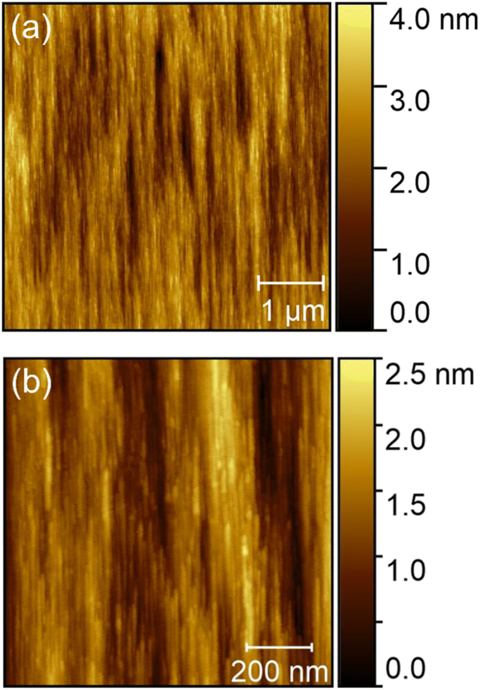 | ||
| Fig. 2 Atomic force microscopy images of a β-Ga2O3 wafer subjected to 46 growth/etch-back cycles. (a) 5 × 5 μm image with RMS roughness = 1.6 nm. (b) 1 × 1 μm image with RMS roughness = 0.7 nm. Elongated features are aligned along the [001] direction and are commonly observed after Ga etching of (010) oriented Ga2O3.41 | ||
III. Results and discussion
1. RHEED surface reconstruction growth map
(InxGa1−x)2O3 growths were performed at BandiT calibrated growth temperatures ranging from 592–771 °C, Ga fluxes ranging from 0.5–2.0 × 10⁻⁷ torr, and In fluxes ranging from 0–1.0 × 10⁻⁶ torr at a fixed oxygen plasma power of 250 W and 3.00 SCCM flow. Growth durations ranged from 2 to 15 minutes ending with the stabilization of one of two distinct RHEED patterns shown in Fig. 3. The terminal RHEED patterns are a streaky 2× surface reconstruction typical of the 〈001〉 azimuth of β-Ga2O3 (Fig. 3a) or a spotty/faceted pattern attributed to the formation of bixbyite In2O3 on the growth surface (Fig. 3b). The evolution of the principal streaks into the broad spots in Fig. 3b indicates significant surface roughening and transmission through a distinct crystal phase on the growth surface, while the appearance of three higher-order spots in between the principal (01) spots suggests the formation of facets with approximately 4× the periodicity of the crystal lattice. Additionally, the d-spacing of the principal spots/streaks increases from 5.8 Å for ungrown β-Ga2O3 to 7.1 Å for the spotty/faceted pattern in Fig. 3b. These diffraction spots are consistent with diffraction from the bixbyite (110) plane with RHEED pattern periodicity .42 The possible orientation of bixbyite In2O3 on (010) β-Ga2O3 is shown in the ESI.† The typical time to stabilize the spotty/faceted pattern in Fig. 3b is 2–3 minutes. In contrast the streaky 2× surface reconstruction is stable to 15 minutes or longer, with some degradation in (00) and (01) FWHM over time observed at transitional growth conditions (discussed below). Crucially, however, the lattice d-spacing remains stable and the periodicity of the 2× reconstruction does not change.
 | ||
| Fig. 3 Terminal RHEED patterns of (a) streaky 2× surface reconstruction typical of Ga2O3 growth, and (b) spotty/faceted pattern typical of low-temperature, Ga-lean growth. Streaks are labeled with d-spacing relative to the (00) streak. The {01} streak d-spacing for the spotty/faceted pattern in (b) is attributed to diffraction from the bixbyite In2O3 (110) plane. | ||
Fig. 4 shows the growth map of (InxGa1−x)2O3 alloys as a function growth temperature, Ga flux, and In flux space. This RHEED data for this growth map was collected by the cyclical growth/etch method and analyzed using a machine learning algorithm with a LPIPS metric and CLAHE pre-processing. The terminal RHEED patterns for each growth setpoint were classified as either streaky 2× (similar to Fig. 3a) or spotty/faceted (similar to Fig. 3b). The Ga and In beam equivalent pressures were converted into particle fluxes according to the procedure in the ESI.† The particle fluxes and resulting metal/oxygen ratio (Ga + In)2O3 are plotted in Fig. 4b–d. A growth boundary between the two classes of RHEED patterns is observed, with lower growth temperatures and lower metal fluxes resulting in the spotty/faceted pattern associated with formation of bixbyite In2O3. Above approximately 725 °C growth temperature, or metal/oxygen flux ratio greater than 2/3, the bixbyite In2O3 RHEED pattern is suppressed and the growth surface exhibits a 2× reconstruction typical of monoclinic phase In-catalyzed Ga2O3 or (InxGa1−x)2O3 growth. The growth boundary is strongly dependent on growth temperature and total metal/oxygen flux ratio, with relatively weak dependence on the In flux.
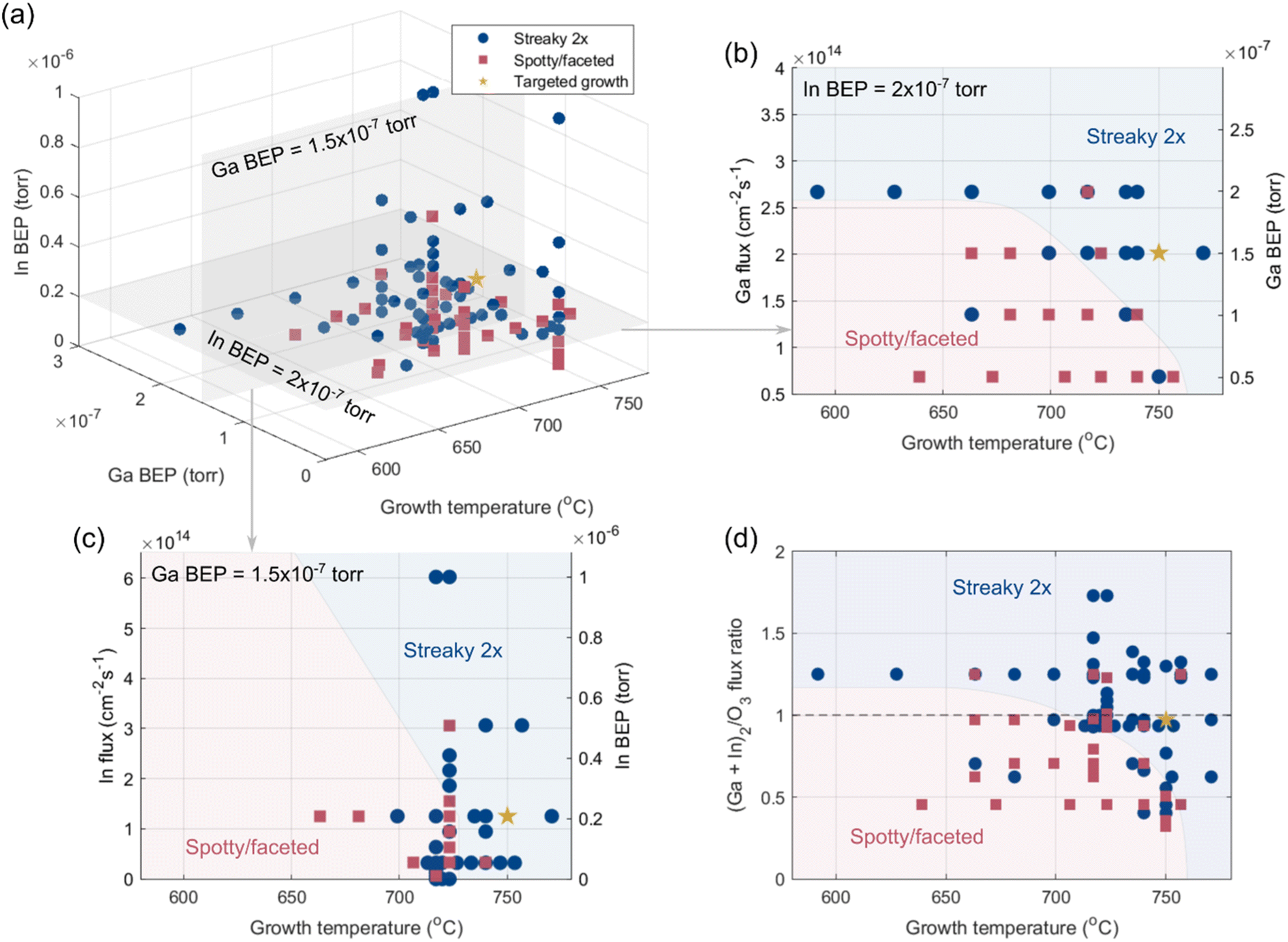 | ||
| Fig. 4 Growth map of (InxGa1−x)2O3 alloys obtained from cyclical growth/etch experiments with results classified by similarity analysis. (a) RHEED surface reconstruction vs. Ga BEP, In BEP, and growth temperature Tg. Blue circles: streaky 2× reconstruction stabilized. Red squares: spotty/faceted reconstruction. Gold star: targeted thick growth. (b) Reconstruction as a function of Tg and Ga flux at In BEP = 2 × 10⁻⁷ torr. (c) Reconstruction as a function of Tg and In flux at Ga BEP = 2 × 10⁻⁷ torr. (d) Reconstruction as a function of Tg and stoichiometric flux ratio (Ga + In)2/O3. Shaded regions are guides to the eye. | ||
It's notable that the (InxGa1−x)2O3 alloy growth map shown in Fig. 4 was created using automated machine learning algorithm LPIPS for RHEED pattern recognition, rather than traditional manual labeling and sorting of RHEED patterns. Unlike traditional metrics such as Mean Squared Error (MSE) or Peak Signal-to-Noise Ratio (PSNR) that analyze images on a pixel level, the LPIPS metric used here operates in a feature space. In this scenario, the architecture of a pre-trained CNN known as AlexNet43 can be employed to extract features from images. Briefly, a feature space is a representation where images are characterized by a set of descriptors, or features, that encapsulate informative aspects beyond pixel values, such as edges, textures, or shapes. Through AlexNet, LPIPS transforms the images into this feature space, facilitating a comparison that highlights more meaningful similarity between images. This approach has shown alignment with human perceptual judgments across various datasets and image distortions, providing a more perceptually aligned measure of similarity.40
2. Chemistry of In-catalyzed (InxGa1−x)2O3 growth
Epitaxial growth of the ternary alloy (InxGa1−x)2O3 has proven more challenging than (AlxGa1−x)2O3 due to the unique (In,Ga) oxide growth chemistry variously referred to as metal oxide catalyzed epitaxy (“MOCATAXY”)44–46 or metal-exchange catalysis (“MEXCAT”).47,48 The addition of In flux during MBE growth of Ga2O3 results in a 2-step reaction characterized by the formation of In2O3 followed by metal exchange between Ga and In to form β-Ga2O3:49| 2In(a) + 3O(a) → In2O3(s) | (1) |
| 2Ga(a) + In2O3(s) → Ga2O3(s) + 2In(a) | (2) |
This metal exchange reaction increases the effective oxygen reservoir at the growth surface due to the higher oxidation efficiency of In compared to Ga,34,49 resulting in an increase in Ga2O3 growth rate. However, negligible In incorporation occurs in this In-catalyzed growth regime,41,44–49 with the remaining adsorbed indium in reaction (2) desorbing from the growth surface. MBE growth conditions for incorporating indium in single crystal monoclinic (InxGa1−x)2O3 alloys remain elusive. Mauze et al. reported In incorporation up to approximately 24% mole fraction for MBE growth at low Ga/O flux ratio at 900 °C and 800 °C on (010) and (001) oriented Ga2O3 substrates, respectively.45 Von Wenckstern et al. synthesized polycrystalline (InxGa1−x)2O3 across the entire composition range by pulsed laser deposition on c-plane sapphire.50 Few reports of successful synthesis of thick monoclinic (InxGa1−x)2O3 epilayers with non-negligible In mole fractions exist.44,45
An additional unique characteristic of β-Ga2O3 MBE growth is etching under Ga-rich conditions. The Ga2O3 growth rate decreases with increasing Ga/O flux ratio due to the formation of the volatile suboxide Ga2O:34,51,52
| 4Ga(a) + Ga2O3(s) → 3Ga2O(a) | (3) |
Ga2O readily desorbs at typical growth temperatures resulting in negative growth rate, or etching, under Ga/O flux ratios greater than three.34,52 Furthermore, highly Ga-rich conditions lead to etching of (InxGa1−x)2O3 as In is readily exchanged by Ga according to reaction (2) to form Ga2O3, followed by subsequent desorption of adsorbed In and Ga2O according to reaction (3).
Based on the eqn (1)–(3) presented above, the (InxGa1−x)2O3 alloy map presented in Fig. 4 can be explained by the chemistry of In-catalyzed growth in a two-step process:
(a) In the first step, adsorbed In is preferentially oxidized to form either In2O3 or In2O on the growth surface at all growth temperatures investigated. There are three reaction regimes based on the In/oxygen flux ratio  . In the oxygen-rich regime with rIn < 1, In2O3 forms with excess adsorbed oxygen similar to eqn (1):53
| 2rInIn(a) + 3O(a) → rInIn2O3(s) + 3(1 − rIn)O(a) | (4) |
In the moderately In-rich regime (ii) with 1 < rIn < 3, excess In reacts with In2O3 to form In2O, reducing the total amount of In2O3 on the surface:41
| 2rInIn(a) + 3O(a) → In2O3(s) + 2(rIn − 1)In(a), | (5a) |
 | (5b) |
In the highly In-rich regime with rIn > 3, only adsorbed In2O and In are present similar to eqn (3):
| 2rInIn(a) + 3O(a) → 3In2O(a) + 2(rIn − 3)In(a) | (6) |
(b) In the second step, Ga flux reacts with both excess adsorbed O to directly form Ga2O3 and with In2O3 by means of the cation exchange reaction (2) to form the alloy (InxGa1−x)2O similar to eqn (2):
| 2(1 − x)Ga(a) + In2O3(a) → (InxGa1−x)2O3(s) + 2(1 − x)In(a) | (7) |
Direct formation of (InxGa1−x)2O3 from adsorbed Ga, In, and O is inhibited by the preferential oxidation of In.53 Cation exchange between Ga and In2O3 is therefore expected to be the primary reaction pathway for growth of (InxGa1−x)2O3.
Excess adsorbed Ga may decompose the (InxGa1−x)2O3 film in a modified version of reactions (2) and (3):54
| 2(rGa − (1 − x))Ga(a) + (InxGa1−x)2O3(s) → 2xIn(a) + Ga2O3(s) + 2(rGa − 1)Ga(a), | (8a) |
 | (8b) |
 . The excess Ga first displaces In from (InxGa1−x)2O3 to form Ga2O3 and adsorbed In, and subsequently decomposes Ga2O3 to form the suboxide Ga2O. The adsorbed In and Ga2O readily desorb at the growth temperatures investigated,52,55 resulting in only a Ga2O3 film remaining.
At sufficiently high Ga flux and growth temperatures above ∼725 °C, Ga exchange with In occurs according to reactions (2) and (6), consuming the In2O3 and forming (InxGa1−x)2O3 or Ga2O3. However, this cation exchange process is inhibited at low growth temperatures54 and low Ga fluxes, resulting in the accumulation of In2O3 on the growth surface and the appearance of the spotty/faceted surface reconstruction. Additionally, increasing the In flux at high growth temperatures does not result in the accumulation of In2O3 as the excess In flux instead forms volatile In2O according to reaction (5). The spotty/faceted RHEED pattern associated with bixbyite In2O3 is therefore only stabilized under relatively low growth temperature, low metal flux conditions where In2O3 is not consumed by either Ga cation exchange or by In2O suboxide formation.
3. In-plane lattice spacing analysis from RHEED
In the cyclical MBE methodology, sample characterization may be accomplished using techniques compatible with ultra-high vacuum growth, such as spectroscopic ellipsometry, mass spectroscopy, or RHEED. In particular, RHEED is a highly surface-sensitive technique that probes the first few atomic layers of the sample36,37 and is capable of monitoring crystal growth in real time. RHEED provides information about surface chemistry and reconstruction, lattice periodicity, surface roughness, crystalline phases and domain size, growth rate, and growth mode (e.g. layer-by-layer vs. step flow) for thin films.36,37,56,57 The ability to measure lattice periodicity, corresponding to crystal phase and composition, and diffraction pattern FWHM, corresponding to surface roughness and domain size, in a real-time manner make RHEED uniquely suited to the study of cyclical growth and etch of β-Ga2O3 based alloys.RHEED offers a wealth of information about crystal growth. The d-spacing of the first-order streaks directly measures the lattice periodicity of the uppermost atomic layers of the growing crystal. The FWHM of the (00) streak measures the crystal domain size and is correlated with surface roughness. The periodicity of the surface reconstruction, e.g. 2×, is directly related to the chemical bonds and crystal phase present at the sample surface. The appearance of bright diffraction spots indicates beam transmission through a roughened surface of 3D islands.36,57 Finally, the intensity of the specular reflection and its evolution with time provide information about growth mode.37,56 For example, layer-by-layer (Frank-van der Merwe) growth results in oscillations in RHEED intensity. The period of this oscillation is the time to form a complete monolayer. In contrast, step-flow growth and island growth does not result in intensity oscillations. By tracking the evolution of these RHEED features over time, a nearly complete picture of crystal growth is deduced.
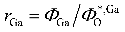
RHEED was used to analyze a change in the in-plane lattice spacing between the principal RHEED streaks during the (InxGa1−x)2O3 growth in many growth conditions. The percentage change in d-spacing between the (01) and (0![[1 with combining macron]](https://www.rsc.org/images/entities/char_0031_0304.gif) ) streaks is shown for an In flux dependent growth series in Fig. 5. The percentage change in d-spacing is normalized to the β-Ga2O3c-plane lattice constant according to [(2d − c)/c] × 100%. The d-spacing does not change with time for homoepitaxial growth of Ga2O3 at 723 °C and 1.5 × 10⁻⁷ torr Ga flux. The d-spacing increases by as much as 1.2% immediately upon initiation of (InxGa1−x)2O3 growth with In flux ranging from 1 × 10⁻⁷ to 3 × 10⁻⁷ torr. The d-spacing increases slowly for In flux of 3–4 × 10⁻⁷ torr and contracts slightly for high In fluxes of 5 × 10⁻⁷ torr and greater. Expansion of the d-spacing is associated with the growth of an In-containing film with larger unit cell than the β-Ga2O3 substrate, since the crystal termination layer is free to reconstruct and may relax with respect to the substrate lattice constants, even if the underlying bulk crystal is fully strained. The rapid increase in d-spacing at the beginning of growth, and subsequent slow decrease, suggest that lower In fluxes of 1 × 10⁻⁷ to 3 × 10⁻⁷ torr result in growth of initially In-rich films with decreasing In incorporation over time. Vegard's law interpolation of the β-Ga2O3 and monoclinic In2O3c-plane lattice constants indicates approximately 10% In mole fraction for a d-spacing increase of 1%.31,33 By contrast, growth at high In fluxes does not result in a significant change in d-spacing, suggesting negligible In incorporation.
) streaks is shown for an In flux dependent growth series in Fig. 5. The percentage change in d-spacing is normalized to the β-Ga2O3c-plane lattice constant according to [(2d − c)/c] × 100%. The d-spacing does not change with time for homoepitaxial growth of Ga2O3 at 723 °C and 1.5 × 10⁻⁷ torr Ga flux. The d-spacing increases by as much as 1.2% immediately upon initiation of (InxGa1−x)2O3 growth with In flux ranging from 1 × 10⁻⁷ to 3 × 10⁻⁷ torr. The d-spacing increases slowly for In flux of 3–4 × 10⁻⁷ torr and contracts slightly for high In fluxes of 5 × 10⁻⁷ torr and greater. Expansion of the d-spacing is associated with the growth of an In-containing film with larger unit cell than the β-Ga2O3 substrate, since the crystal termination layer is free to reconstruct and may relax with respect to the substrate lattice constants, even if the underlying bulk crystal is fully strained. The rapid increase in d-spacing at the beginning of growth, and subsequent slow decrease, suggest that lower In fluxes of 1 × 10⁻⁷ to 3 × 10⁻⁷ torr result in growth of initially In-rich films with decreasing In incorporation over time. Vegard's law interpolation of the β-Ga2O3 and monoclinic In2O3c-plane lattice constants indicates approximately 10% In mole fraction for a d-spacing increase of 1%.31,33 By contrast, growth at high In fluxes does not result in a significant change in d-spacing, suggesting negligible In incorporation.
 | ||
| Fig. 5 Percentage change in d-spacing relative to the Ga2O3c plane lattice constant vs. growth time for (0) to (01) streak spacing. All (InGa)2O3 growths were performed at 723 °C and Ga BEP = 1.5 × 10⁻⁷ torr. In BEP in torr is indicated by color bar and varies from zero to 1 × 10⁻⁶ torr. | ||
This counter-intuitive trend of decreasing In incorporation vs. increasing In flux can be explained by the reaction eqn (4) through (6). At low In fluxes corresponding to the oxygen-rich regime (eqn (4)), In2O3 is readily formed and cation exchange with Ga occurs to form (InxGa1−x)2O3. The formation of (InxGa1−x)2O3 subtracts from the amount of In2O3 present on the growth surface, leading to a gradual reduction in the growth rate and In content of (InxGa1−x)2O3 over time. This is evident in the drop in d-spacing vs. time for In fluxes ranging from 1–2 × 10⁻⁷ torr. As the In flux increases to the moderately In-rich regime, In2O suboxide formation reduces the amount of In2O3 available for Ga cation exchange, evident in the markedly smaller initial d-spacing shift for In fluxes ranging from 2.5–4 × 10⁻⁷ torr. In the highly In-rich regime (eqn (5)), no In2O3 is formed and all available oxygen flux is consumed as In2O. Therefore either no film growth occurs, or only a homoepitaxial Ga2O3 film with negligible In incorporation is grown, and the d-spacing remains constant with time. Under highly In-rich conditions with flux greater than 5 × 10⁻⁷ torr, Ga suboxide etching is again expected to occur since no adsorbed oxygen is present and the adsorbed Ga flux can react only with the Ga2O3 substrate.
4. Ex situ analysis of targeted (InxGa1−x)2O3 growth
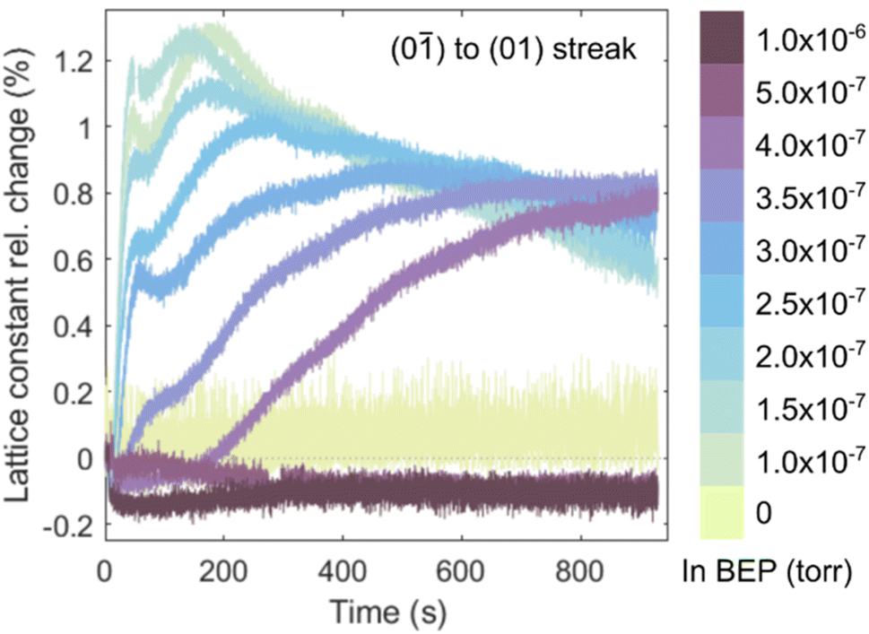
A targeted growth was conducted based on the RHEED surface reconstruction map in Fig. 4. Growth conditions were selected within the streaky 2× region and near the boundary with spotty/faceted In2O3 growth, and (InxGa1−x)2O3 was grown for 4 hours. These conditions were expected to yield significant In incorporation in monoclinic (InxGa1−x)2O3.Fig. 6a shows a XRD reciprocal space map (RSM) about the β-Ga2O3 (420) reflection for the 4-hour long targeted growth performed at 750 °C, 1.5 × 10⁻⁷ torr Ga flux, and 2.0 × 10⁻⁷ torr In flux. A high resolution coupled ω–2θ scan about the (020) reflection is shown inset. Significant In incorporation is evident from the compressively strained features at low reciprocal space coordinate qz. The film is coherently strained to the β-Ga2O3 substrate with only minimal relaxation to lower reciprocal space coordinate qx. The RSM confirms that (InxGa1−x)2O3 alloy growth is the monoclinic C2/m phase and phase separation does not occur. The absence of a single well-defined compressive peak in the coupled ω–2θ scan indicates that In incorporation is highly non-uniform in the growth direction.
 | ||
| Fig. 6 Ex situ characterization of high-In content targeted (InGa)2O3 growth. (a) Reciprocal space map of (420) plane. Growth conditions are labeled directly on figure. Inset: coupled ω–2θ scan of (020) plane. (b) Depth profiles of atomic concentration of Ga, In, and O for high-In content targeted thick (InxGa1−x)2O3 growth. XPS measurement is shown by solid lines. The simulated depth profile for RBS measurements is shown as dot-dashed curves. Indium concentration curves are scaled by a factor of 10 for clarity. | ||
Fig. 6b shows the XPS and simulated RBS atomic concentration depth profiles for the targeted growth. The indium concentration curves are scaled by a factor of 10 for clarity. The atomic concentrations at the sample surface are reduced due to the presence of a thin Au layer deposited to prevent sample charging during RBS measurements. Peak In mole fraction of x = 5.6% in (InxGa1−x)2O3 is observed. The In mole fraction decreases in the growth direction, in qualitative agreement with the RHEED d-spacing decrease over time observed in Fig. 5. The simulated film thickness is approximately 980 nm. Additional targeted growths conducted at higher Ga fluxes (not shown) did not yield In incorporation measurable by XPS or RBS. This illustrates the competition between In-incorporating (InxGa1−x)2O3versus In-catalyzed Ga2O3 growth regimes. In incorporation is achieved at reduced Ga fluxes, in agreement with previous studies54,58 which indicated full In incorporation at very low metal/oxygen ratios (highly oxygen rich growth). The In-catalyzed growth regime at higher Ga fluxes achieves high growth rates, however In incorporation is suppressed.
IV. Summary and conclusions
In summary, the results of the cyclical growth/etch RHEED experiments and the targeted thick growth paint a complete picture of the growth space for MBE grown monoclinic (InxGa1−x)2O3 alloys. Growth proceeds as a two-step process characterized by the preferential oxidation of adsorbed In followed by cation exchange with adsorbed Ga. At low growth temperatures below approximately 725 °C, cation exchange is inhibited and bixbyite In2O3 forms. At high growth temperatures, cation exchange occurs and (InxGa1−x)2O3 growth is dominated by the effective metal/oxygen flux ratios. Low metal flux ratios, i.e. oxygen rich growth, yield maximum In incorporation at the expense of low growth rate. Counter-intuitively, moderately In-rich growth with 1 < rIn < 3 results in a reduction of In incorporation and growth rate due to the formation of In2O suboxide. Very In-rich growth with rIn > 3 results in no film growth, or only very slow growth of bixbyite In2O3, due to nearly complete consumption of all available oxygen flux as In2O. Increasing rGa at low to moderate rIn results in reduced In incorporation but increased (InxGa1−x)2O3 growth rate due to Ga cation exchange. As rGa is increased further to moderately Ga-rich conditions, Ga2O suboxide formation decomposes the (InxGa1−x)2O3 film and reduces both In incorporation and growth rate further. Adsorbed In displaced from the (InxGa1−x)2O3 film readily desorbs at these growth temperatures, with the result that the growth surface maintains a streaky 2× surface reconstruction typical of Ga2O3 homoepitaxial growth. MBE growth at conditions near the RHEED surface reconstruction boundary between streaky 2× and spotty/faceted patterns is therefore expected to yield maximum In incorporation at a given (InxGa1−x)2O3 growth rate determined by the Ga flux. The RHEED streak d-spacing provides a measure of the epilayer lattice constant, and its evolution vs. time illustrates the non-uniform nature of In incorporation in (InxGa1−x)2O3. This non-uniform composition is confirmed by ex situ XRD and RBS measurements of a targeted growth which exhibits peak In mole fraction of 5.6% in a coherently strained monoclinic (InxGa1−x)2O3 film. Future work could focus on optimization of In incorporation uniformity and material quality by real-time control of Ga and In flux and/or substrate temperature.The cyclical oxide growth and etch-back method developed in this work stands apart from traditional MBE growth techniques which rely on unidirectional material deposition. Leveraging the unique sub-oxide desorption under metal flux and a differentially pumped RHEED system, a six-fold improvement in experimental throughput was achieved. The growth and etch-back process is remarkably repeatable, with full recovery of the β-Ga2O3 substrate growth surface roughness (∼1 nm) achieved up to 46 cycles on a single wafer. Indefinite substrate re-use can be achieved with an In-free mounting scheme. RHEED images of surface reconstruction, line scans of streak d-spacing and FWHM vs. time, and streak intensity profiles provide both qualitative and quantitative feedback to the grower in real-time. This cyclical growth and etch-back method can be applied to other material systems exhibiting incongruent subcomponent evaporation from a two-phase mixture, including both oxides (e.g. GeO2, SnO2) and other chemistries (e.g. In2Se3, InSe). In addition to the examples of Ga2O3 and In2O3 investigated here, this class of oxide materials includes numerous rare earth-oxides, lanthanide-oxides, and the wide-bandgap group IV-oxides SiO2, SnO2, and GeO2 which evaporate as IV(a) + IVO2(s) → 2IVO(g).35 GeO2 is a material of particular interest as it has an ultra wide bandgap of 4.6–4.7 eV (ref. 59) and theoretically predicted ambipolar dopability (i.e. n and p type conductivity).60 GeO2 remains elusive to growth by MBE61 and mist CVD.62 Further refinements in RHEED image analysis will complement this inherently high-throughput experimental methodology to rapidly characterize the growth space for both Ga2O3 based alloys and other emerging materials.
Author contributions
Stephen Schaefer: conceptualization, data curation, formal analysis, investigation, methodology, visualization, writing (original draft). Davi Febba: formal analysis, data curation, investigation, methodology, software, validation, writing (original draft). Kingsley Egbo: investigation, methodology, resources, writing (editing and review). Glenn Teeter: investigation, methodology, resources. Andriy Zakutayev: conceptualization, funding acquisition, supervision, writing (editing and review). Brooks Tellekamp: conceptualization, formal analysis, funding acquisition, investigation, methodology, project administration, resources, supervision, writing (editing and review).Conflicts of interest
There are no conflicts of interest to declare.Acknowledgements
This work was authored by the National Renewable Energy Laboratory (NREL), operated by Alliance for Sustainable Energy, LLC, for the US Department of Energy (DOE) under Contract No. DE-AC36-08GO28308. Funding for materials synthesis and characterization was provided by the Laboratory Directed Research and Development (LDRD) Program at NREL. Funding for analysis, software, and validation was provided by the Office of Energy Efficiency and Renewable Energy (EERE), Advanced Materials and Manufacturing Technologies Office. The views expressed in the article do not necessarily represent the views of the DOE or the US Government.References
- A. Y. Cho and J. R. Arthur, Molecular Beam Epitaxy, Prog. Solid State Chem., 1975, 10(3), 157–191 CrossRef.
- J. Y. Tsao, Materials Fundamentals of Molecular Beam Epitaxy, Academic Press Inc., San Diego, 1993 Search PubMed.
- M. A. Herman and H. Sitter, Molecular Beam Epitaxy: Fundamentals and Current Status, Springer-Verlag, Berlin, 2nd edn, 1996 Search PubMed.
- E. F. Schubert, Doping in III-V Semiconductors, Cambridge University Press, Cambridge, 1995 Search PubMed.
- E. C. Larkins, E. S. Hellman, D. G. Schlom, J. S. Harris Jr, M. H. Kim and G. E. Stillman, Reduction of the acceptor impurity background in GaAs grown by molecular beam epitaxy, Appl. Phys. Lett., 1986, 49(7), 391–393 CrossRef CAS.
- J. P. Eisenstein, K. B. Cooper, L. N. Pfeiffer and K. W. West, Insulating and Fractional Quantum Hall States in the First Excited Landau Level, Phys. Rev. Lett., 2002, 88, 076801 CrossRef CAS PubMed.
- V. Umansky, M. Heiblum, Y. Levinson, J. Smet, J. Nubler and M. Dolev, MBE growth of ultra-low disorder 2DEG with mobility exceeding 35 × 106 cm2/V s, J. Cryst. Growth, 2009, 311, 1658 CrossRef CAS.
- C. Reichl, MBE Growth of Ultrahigh-Mobility 2DEGs in GaAs/AlGaAs, Universität Regensburg, 2014 Search PubMed.
- J. Faist, F. Capasso, D. L. Sivco, C. Sirtori, A. L. Hutchinson and A. Y. Cho, Quantum Cascade Laser, Science, 1994, 264, 553–556 CrossRef CAS PubMed.
- T. Mimura, S. Hiyamizu, T. Fujii and K. Nanbu, A New Field-Effect Transistor with Selectively Doped GaAs/n-AlxGa1-xAs Heterojunctions, Jpn. J. Appl. Phys., 1980, 19(5), L225–L227 CrossRef CAS.
- T. Matsumoto, M. Aoki, A. Kinoshita and T. Aono, Absorption and Reflection of Vapor Grown Single Crystal Platelets of β-Ga2O3, Jpn. J. Appl. Phys., Part 1, 1974, 13, 1578 CrossRef CAS.
- M. Higashiwaki, K. Sasaki, A. Kuramata, T. Masui and S. Yamakoshi, Gallium oxide (Ga2O3) metal-semiconductor field-effect transistors on single-crystal β-Ga2O3 (010) substrates, Appl. Phys. Lett., 2012, 100, 013504 CrossRef.
- A. Kuramata, K. Koshi, S. Watanabe, Y. Yamaoka, T. Masui and S. Yamakoshi, High-quality β-Ga2O3 single crystals grown by edge-defined film-fed growth, Jpn. J. Appl. Phys., 2016, 55, 1202A2 CrossRef.
- M. Higashiwaki, K. Sasaki, H. Murakami, Y. Kumagai, A. Koukitu, A. Kuramata, T. Masui and S. Yamakoshi, Recent progress in Ga2O3 power devices, Semicond. Sci. Technol., 2016, 31, 034001 CrossRef.
- E. Ahmadi, O. S. Koksaldi, X. Zheng, T. Mates, Y. Oshima, U. K. Mishra and J. S. Speck, Demonstration of β-(AlxGa1−x)2O3/β-Ga2O3 modulation doped field-effect transistors with Ge as dopant grown via plasma-assisted molecular beam epitaxy, Appl. Phys. Express, 2017, 10, 071101 CrossRef.
- S. J. Pearton, J. Yang, P. H. Cary IV, F. Ren, J. Kim, M. J. Tadjer and M. A. Mastro, A review of Ga2O3 materials, processing, and devices, Appl. Phys. Rev., 2018, 5, 011301 Search PubMed.
- Y. Zhang and J. S. Speck, Importance of shallow hydrogenic dopants and material purity of ultra-wide bandgap semiconductors for vertical power electron devices, Semicond. Sci. Technol., 2020, 35, 125018 CrossRef CAS.
- K. N. Heinselman, D. Haven, A. Zakutayev and S. B. Reese, Projected Cost of Gallium Oxide Wafers from Edge-Defined Film-Fed Crystal Growth, Cryst. Growth Des., 2022, 22(8), 4854–4863 CrossRef CAS.
- R. Singh, T. R. Lenka, D. K. Panda, R. T. Velpula, B. Jain, H. Q. T. Bui and H. P. T. Nguyen, The dawn of Ga2O3 HEMTs for high power electronics - a review, Mater. Sci. Semicond. Process., 2020, 119, 105216 CrossRef CAS.
- T. Oshima, Y. Kato, N. Kawano, A. Kuramata, S. Yamakoshi, S. Fujita, T. Oishi and M. Kasu, Carrier confinement observed at modulation-doped β-(AlxGa1-x)2O3/Ga2O3 heterojunction interface, Appl. Phys. Express, 2017, 10, 035701 CrossRef.
- S. Krishnamoorthy, Z. Xia, C. Joishi, Y. Zhang, J. McGlone, J. Johnson, M. Brenner, A. R. Arehart, J. Hwang, S. Lodha and S. Rajan, Modulation-Doped β-(Al0.2Ga0.8)2O3/Ga2O3 Field-Effect Transistor, Appl. Phys. Lett., 2017, 111, 023502 CrossRef.
- Y. Zhang, A. Neal, Z. Xia, C. Joishi, J. M. Johnson, Y. Zheng, S. Bajaj, M. Brenner, D. Dorsey, K. Chabak, G. Jessen, J. Hwang, S. Mou, J. P. Heremans and S. Rajan, Demonstration of high mobility and quantum transport in modulation-doped β-(AlxGa1-x)2O3/Ga2O3 heterostructures, Appl. Phys. Lett., 2018, 112, 173502 CrossRef.
- Y. Zhang, C. Joishi, Z. Xia, M. Brenner, S. Lodha and S. Rajan, Demonstration of β-(AlxGa1-x)2O3/Ga2O3 double heterostructure field effect transistors, Appl. Phys. Lett., 2018, 112, 233503 CrossRef.
- X. Chen, F. Ren, S. Gu and J. Ye, Review of gallium-oxide-based solar-blind ultraviolet photodetectors, Photonics Res., 2019, 7(4), 381–415 CrossRef CAS.
- T.-H. Chang, S.-J. Chang, C. J. Chiu, C.-Y. Wei, Y.-M. Juan and W.-Y. Weng, Bandgap-Engineered in Indium–Gallium–Oxide Ultraviolet Phototransistors, IEEE Photonics Technol. Lett., 2015, 27, 8 Search PubMed.
- Z. Zhang, H. von Wenckstern, J. Lenzner, M. Lorenz and M. Grundmann, Visible-blind and solar-blind ultraviolet photodiodes based on (InxGa1-x)2O3, Appl. Phys. Lett., 2016, 108, 123503 CrossRef.
- F. Alema, B. Hertog, O. Ledyaev, D. Volovik, G. Thoma, R. Miller, A. Osinsky, P. Mukhopadhyay, S. Bakhshi, H. Ali and W. V. Schoenfeld, Solar blind photodetector based on epitaxial zinc doped Ga2O3 thin film, Phys. Status Solidi A, 2017, 214(5), 1600688 CrossRef.
- D. Guo, Z. Wu, Y. An, X. Li, X. Guo, X. Chu, C. Sun, M. Lei, L. Li, L. Cao, P. Li and W. Tang, Room temperature ferromagnetism in (Ga1-xMnx)2O3 epitaxial thin films, J. Mater. Chem. C, 2015, 3, 1830 RSC.
- R. Korlacki, M. Hilfiker, J. Knudtson, M. Stokey, U. Kilic, A. Mauze, Y. Zhang, J. Speck, V. Darakchieva and M. Schubert, Strain and Composition Dependencies of the Near-Band-Gap Optical Transitions in Monoclinic (AlxGa1-x)2O3 Alloys with Coherent Biaxial In-Plane Strain on Ga2O3 (010), Phys. Rev. Appl., 2022, 18, 064019 CrossRef CAS.
- H. Peelaers, J. B. Varley, J. S. Speck and C. G. Van de Walle, Structural and electronic properties of Ga2O3-Al2O3 alloys, Appl. Phys. Lett., 2018, 112, 242101 CrossRef.
- X. Liu and C.-K. Tan, Electronic properties of monoclinic (InxGa1-x)2O3 alloys by first-principle, AIP Adv., 2019, 9, 035318 CrossRef.
- H. Peelaers, D. Steiauf, J. B. Varley, A. Janotti and C. G. Van de Walle, (InxGa1-x)2O3 alloys for transparent electronics, Phys. Rev. B: Condens. Matter Mater. Phys., 2015, 92, 085206 CrossRef.
- J. Åhman, G. Svensson and J. Albertsson, A Reinvestigation of β-Gallium Oxide, Acta Crystallogr., Sect. C: Cryst. Struct. Commun., 1996, 52, 1336–1338 CrossRef.
- P. Vogt and O. Bierwagen, The competing oxide and sub-oxide formation in metal-oxide molecular beam epitaxy, Appl. Phys. Lett., 2015, 106, 081910 CrossRef.
- K. M. Adkison, S.-L. Shang, B. J. Bocklund, D. Klimm, D. G. Schlom and Z.-K. Liu, Suitability of binary oxides for molecular-beam epitaxy source materials: a comprehensive thermodynamic analysis, APL Mater., 2020, 8, 081110 CrossRef CAS.
- S. Hasegawa, Reflection high energy electron diffraction, in Characterization of Materials, ed. E. N. Kaufmann, John Wiley & Sons, Inc., 2012 Search PubMed.
- W. Braun, Applied RHEED: Reflection High-Energy Electron Diffraction during Crystal Growth, Springer-Verlag, Berlin, Heidelberg, 1st edn, 1999 Search PubMed.
- B. Tellekamp, K. N. Heinselman, S. Harvey, I. S. Khan and A. Zakutayev, Growth and characterization of homoepitaxial β-Ga2O3 layers, J. Phys. D: Appl. Phys., 2020, 53, 484002 CrossRef.
- E. Ahmadi, Y. Oshima, F. Wu and J. S. Speck, Schottky barrier height of Ni to β-(AlxGa1−x)2O3 with different compositions grown by plasma-assisted molecular beam epitaxy, Semicond. Sci. Technol., 2017, 32, 035004 CrossRef.
- R. Zhang, P. Isola, A. A. Efros, E. Shechtman and O. Wang, The Unreasonable Effectiveness of Deep Features as a Perceptual Metric, in 2018 IEEE/CVF Conference on Computer Vision and Pattern Recognition, 2018, pp. 586–595 Search PubMed.
- P. Mazzolini, P. Vogt, R. Schewski, C. Wouters, M. Albrecht and O. Bierwagen, Faceting and metal-exchange catalysis in (010) β-Ga2O3 thin films homoepitaxially grown by plasma-assisted molecular beam epitaxy, APL Mater., 2019, 7, 022511 CrossRef.
- M. Marezio, Refinement of the crystal structure of In2O3 at two wavelengths, Acta Crystallogr., 1966, 20, 723 CrossRef CAS.
- A. Krizhevsky, I. Sutskever and G. E. Hinton, ImageNet Classification with Deep Convolutional Neural Networks, in Advances in Neural Information Processing Systems, 2012, vol. 25 Search PubMed.
- P. Vogt, A. Mauze, F. Wu, B. Bonef and J. S. Speck, Metal-oxide catalyzed epitaxy (MOCATAXY): the example of the O plasma-assisted molecular beam epitaxy of β-(AlxGa1-x)2O3/β-Ga2O3 heterostructures, Appl. Phys. Express, 2018, 11, 115503 CrossRef.
- A. Mauze, Y. Zhang, T. Itoh, F. Wu and J. S. Speck, Metal oxide catalyzed epitaxy (MOCATAXY) of β-Ga2O3 films in various orientations grown by plasma-assisted molecular beam epitaxy, APL Mater., 2020, 8, 021104 CrossRef CAS.
- A. Mauze, Y. Zhang, T. Itoh, E. Ahmadi and J. S. Speck, Sn doping of (010) β-Ga2O3 films grown by plasma-assisted molecular beam epitaxy, Appl. Phys. Lett., 2020, 117, 222102 CrossRef CAS.
- P. Mazzolini, A. Falkenstein, C. Wouters, R. Schewski, T. Markurt, Z. Galazka, M. Martin, M. Albrecht and O. Bierwagen, Substrate-orientation dependence of β-Ga2O3 (100), (010), (001), and (
![[2 with combining macron]](https://www.rsc.org/images/entities/char_0032_0304.gif) 01) homoepitaxy by indium-mediated metal-exchange catalyzed molecular beam epitaxy (MEXCAT-MBE), APL Mater., 2020, 8, 011107 CrossRef CAS.
01) homoepitaxy by indium-mediated metal-exchange catalyzed molecular beam epitaxy (MEXCAT-MBE), APL Mater., 2020, 8, 011107 CrossRef CAS. - P. Mazzolini, A. Falkenstein, Z. Galazka, M. Martin and O. Bierwagen, Offcut-related step-flow and growth rate enhancement during (100) β-Ga2O3 homoepitaxy by metal-exchange catalyzed molecular beam epitaxy (MEXCAT-MBE), Appl. Phys. Lett., 2020, 117, 222105 CrossRef CAS.
- P. Vogt, O. Brandt, H. Riechert, J. Lähnemann and O. Bierwagen, Metal-Exchange Catalysis in the Growth of Sesquioxides: Towards Heterostructures of Transparent Oxide Semiconductors, Phys. Rev. Lett., 2017, 119, 196001 CrossRef PubMed.
- H. von Wenckstern, D. Splith, M. Purfürst, Z. Zhang, Ch. Kranert, S. Müller, M. Lorenz and M. Grundmann, Structural and optical properties of (In,Ga)2O3 thin films and characteristics of Schottky contacts thereon, Semicond. Sci. Technol., 2015, 30, 024005 CrossRef CAS.
- Y. Oshima, E. Ahmadi, S. Kaun, F. Wu and J. S. Speck, Growth and etching characteristics of (001) β-Ga2O3 by plasma-assisted molecular beam epitaxy, Semicond. Sci. Technol., 2018, 33, 015013 CrossRef.
- P. Vogt and O. Bierwagen, Reaction kinetics and growth window for plasma-assisted molecular beam epitaxy of Ga2O3: incorporation of Ga vs. Ga2O desorption, Appl. Phys. Lett., 2016, 108, 072101 CrossRef.
- P. Vogt and O. Bierwagen, Comparison of the growth kinetics of In2O3 and Ga2O3 and their suboxide desorption during plasma-assisted molecular beam epitaxy, Appl. Phys. Lett., 2016, 109, 062103 CrossRef.
- P. Vogt and O. Bierwagen, Kinetics versus thermodynamics of the metal incorporation in molecular beam epitaxy of (InxGa1−x)2O3, APL Mater., 2016, 4, 086112 CrossRef.
- C. B. Alcock, V. P. Itkin and M. K. Horrigan, Vapour Pressure Equations for the Metallic Elements: 298–2500K, Can. Metall. Q., 1984, 23(3), 309–313 CrossRef CAS.
- J. M. Gaines, In-situ characterization of Il/VI molecular beam epitaxy growth using reflection high-energy electron diffraction oscillations, J. Cryst. Growth, 1994, 137, 187–194 CrossRef CAS.
- J. Jo, Y. Tchoe, G.-C. Yi and M. Kim, Real-Time Characterization Using in situ RHEED Transmission Mode and TEM for Investigation of the Growth Behaviour of Nanomaterials, Nature Scientific Reports, 2018, 8, 1694 CrossRef PubMed.
- P. Vogt, Growth Kinetics, Thermodynamics, and Phase Formation of Group-III and IV Oxides during Molecular Beam Epitaxy, Humboldt-Universität, Berlin, 2017 Search PubMed.
- M. Stapelbroek and B. D. Evans, Exciton Structure in the U.V.-Absorption Edge of Tetragonal GeO, Solid State Commun., 1978, 25, 959–962 CrossRef CAS.
- K. Bushick, K. A. Mengle, S. Chae and E. Kioupakis, Electron and hole mobility of rutile GeO2 from first principles: an ultrawide-bandgap semiconductor for power electronics, Appl. Phys. Lett., 2020, 117, 182104 CrossRef CAS.
- S. Chae, H. Paik, N. M. Vu, E. Kioupakis and J. T. Heron, Epitaxial stabilization of rutile germanium oxide thin film by molecular beam epitaxy, Appl. Phys. Lett., 2020, 117, 072105 CrossRef CAS.
- H. Takane and K. Kaneko, Establishment of a growth route of crystallized rutile GeO2 thin film (≥1 μm/h) and its structural properties, Appl. Phys. Lett., 2021, 119, 062104 CrossRef CAS.
Footnote |
| † Electronic supplementary information (ESI) available. See DOI: https://doi.org/10.1039/d3ta07220g |
| This journal is © The Royal Society of Chemistry 2024 |