
 Open Access Article
 This Open Access Article is licensed under a
 Creative Commons Attribution 3.0 Unported Licence
Sn-assisted heteroepitaxy improves ZnTiN2 photoabsorbers†
John S.
Mangum
 *a,
Sijia
Ke
bc,
Melissa K.
Gish
a,
Emily K.
Raulerson
a,
Craig L.
Perkins
a,
Jeffrey B.
Neaton
def,
Andriy
Zakutayev
a and
Ann L.
Greenaway
*a
*a,
Sijia
Ke
bc,
Melissa K.
Gish
a,
Emily K.
Raulerson
a,
Craig L.
Perkins
a,
Jeffrey B.
Neaton
def,
Andriy
Zakutayev
a and
Ann L.
Greenaway
*a
aMaterials Chemical and Computational Science Directorate, National Renewable Energy Laboratory, Golden, Colorado 80401, USA. E-mail: John.Mangum@nrel.gov; Ann.Greenaway@nrel.gov
bDepartment of Materials Science and Engineering, University of California Berkeley, Berkeley, California 94720, USA
cChemical Sciences Division, Lawrence Berkeley National Laboratory, Berkeley, California 94720, USA
dDepartment of Physics, University of California, Berkeley, Berkeley, CA 94720, USA
eMaterials Sciences Division, Lawrence Berkeley National Laboratory, Berkeley, California 94720, USA
fKavli Energy Nanosciences Institute at Berkeley, Berkeley, California 94720, USA
First published on 23rd January 2024
Abstract
Sustainable production of liquid fuels from abundant resources, such as carbon dioxide and water, may be possible through photoelectrochemical processes. Zinc titanium nitride (ZnTiN2) has been recently demonstrated as a potential photoelectrode semiconductor for photoelectrochemical fuel generation due to its ideal bandgap induced by cation disorder, shared crystal structure with established semiconductors, and self-passivating surface oxides under carbon dioxide reduction operating conditions. However, substantial improvements in crystalline quality and optoelectronic properties of ZnTiN2 are needed to enable such applications. In this work, we investigate the heteroepitaxial growth of ZnTiN2 on c-plane (001) sapphire substrates. Growth on sapphire improves crystal quality, while growth on sapphire at elevated temperatures (300 °C) yields highly-oriented, single-crystal-like ZnTiN2 films. When Sn is incorporated during these epitaxial growth conditions, notable improvements in ZnTiN2 film surface roughness and optoelectronic properties are observed. These improvements are attributed to Sn acting as a surfactant during growth and mitigating unintentional impurities such as O and C. The single-crystal-like, 12% Sn-containing ZnTiN2 films exhibit a steep optical absorption onset at the band gap energy around 2 eV, electrical resistivity of 0.7 Ω cm, and a carrier mobility of 0.046 cm2 V−1 s−1 with n-type carrier concentration of 2 × 1020 cm−3. Density functional theory calculations reveal that moderate substitution of Sn (12.5% of the cation sites) on energetically-preferred cation sites has negligible impact on the optoelectronic properties of cation-disordered ZnTiN2. These results are important steps toward achieving high performance PEC devices based on ZnTiN2 photoelectrodes with efficient photon absorption and photoexcited carrier extraction.
1. Introduction
Photoelectrochemical carbon dioxide reduction (PEC CO2R) may be a sustainable method of generating liquid fuels from abundant H2O and CO2, using sunlight as the energy input. Although there are many proposed structures for PEC devices,1 all are based around light-absorbing semiconductors as photoelectrodes, capturing photons and energizing charge carriers that are directed to perform reactions at the semiconductor–electrolyte interface. Such semiconductor photoelectrodes must withstand degradation while in direct contact with the harsh electrochemical environments necessary for PEC processes while maintaining high optoelectronic performance to maintain the flow of charge carriers to drive the PEC reactions. Although PEC CO2R generally operates in less corrosive environments than PEC water splitting, the search for a stable and highly photocatalytically active semiconductor for CO2R photoelectrodes is ongoing.2On one hand, PEC devices based on III–V semiconductors (e.g. GaInP) or Si offer exceptional optoelectronic properties as a result of those materials having highly optimized crystalline quality for photovoltaic applications, but readily degrade in PEC-relevant aqueous environments.3,4 There has been substantial progress in protecting III–V and Si photoelectrodes from corrosion using surface layers, such as TiO2.5–7 However, these protective layers can parasitically absorb incident photons, thereby decreasing device efficiency,8 and certain passivation layers may not be sufficiently stable under conditions necessary for PEC CO2R processes.9 On the other hand, emerging oxide semiconductors such as bismuth vanadate10 are attractive photoelectrode materials due to their long-term stability in harsh aqueous environments. However, these oxide-based material systems commonly lack structurally compatible substrates, which severely limits the production of high-quality films through heteroepitaxial growth methods. Even though these oxide photoelectrodes can remain stable for long durations, they ultimately suffer from inferior optoelectronic properties that limit charge carrier collection and therefore PEC device performance. There is a need for developing novel semiconductors that do not suffer from these inadequacies that impair the III–V and oxide material systems.
An ideal semiconductor for PEC CO2R would couple long-term stability in aqueous electrochemical environments with the lessons from decades of high-quality semiconductor integration. With these criteria in mind, we recently used a co-design approach with high-throughput, combinatorial materials discovery11 to synthesize a new photoabsorber, ZnTiN2, with potential for PEC CO2R applications. ZnTiN2 was predicted12 to have a crystal structure compatible with the established III–N semiconductor system and expected to exhibit self-passivation under electrochemical conditions through the formation of stable surface oxides.13,14 The predicted bandgap of ZnTiN2 (3.5 eV),15 which was calculated using density functional theory (DFT) with a hybrid functional and a cation-ordered unit cell, is too large for effective PEC applications. However, based on prior knowledge of ternary nitride systems, we expected experimentally synthesized ZnTiN2 to exhibit cation-disordering that would sufficiently reduce the bandgap to an appropriate energy for PEC applications (∼2 eV).16,17 Our initial work demonstrated the synthesis of wurtzite-structured (cation-disordered) ZnTiN2 and indicated that the optoelectronic properties and chemical stability of this nitride semiconductor would be highly suitable for PEC CO2R applications.11 Thin films of ZnTiN2 were shown to remain stable under electrochemical polarization in CO2R-relevant conditions following an initial transformation of the surface to a stable oxide layer.
However, the initial high-throughput ZnTiN2 films exhibited a textured, polycrystalline microstructure due to growth on non-templating substrates (Si with native oxide and glass). Grain boundaries in polycrystalline films can be detrimental to device performance by increasing charge carrier scattering, as suggested by the low in-plane mobility of the polycrystalline ZnTiN2,11 and may also provide physical degradation pathways during PEC device operation. Continued work on ZnTiN2 as a photoelectrode material therefore hinges on improvements to the crystalline quality of the material. It is prudent to borrow insights from established high-quality semiconductor synthesis processes to guide the optimization of ZnTiN2 thin film growth, with the goal of developing growth conditions that can enhance the optoelectronic properties of ZnTiN2 to fully realize this photoelectrode material in functional PEC devices.
There are three approaches that can be employed for improving material quality relative to our preliminary ZnTiN2 syntheses:11 (1) using single crystal substrates that are structurally compatible with the wurtzite ZnTiN2 crystal structure to serve as templates for heteroepitaxial film growth,18 (2) enhancing adatom mobility at the growth surface by growing at elevated temperature,19 and (3) using isovalent surfactants, such as Sn in the case of ZnTiN2, to promote two-dimensional layer-by-layer growth.20,21 In addition, high-throughput experimentation, detailed in our previous work,11 can be used to efficiently narrow down the wurtzite ZnTiN2 deposition parameter space after initially implementing these approaches due to differences in Zn and Ti incorporation at elevated deposition temperature and on different substrates.
In this work, by employing these three strategies in concert, we demonstrate significant improvements in ZnTiN2 crystalline quality and optoelectronic properties. X-ray diffraction and electron microscopy indicate heteroepitaxial alignment to c-plane (001) sapphire substrates and a homogeneous single-crystal-like microstructure. Spectroscopic ellipsometry, transient absorption spectroscopy, and Hall effect measurements show a reduction in sub-bandgap optical absorption and longer photoexcited carrier lifetimes along with increased carrier mobility in the optimized Sn-containing ZnTiN2 films. Furthermore, DFT calculations indicate that Sn substitution on energetically-preferred cation sites in cation-disordered ZnTiN2 has negligible effects on the electronic band structure and could alleviate local charge imbalance due to Zn clustering. The combination of these findings demonstrates critical steps in the optimization of ZnTiN2 thin films for use in PEC applications.
2. Results & discussion
2.1 Optimizing ZnTiN2 growth parameters
Compositionally graded libraries of Zn1+xTi1−xN2 thin films were initially deposited on Si, EXG glass, and c-plane (001) Al2O3 (sapphire) at ambient and elevated temperatures following the combinatorial growth procedures outlined in our previous work.11 Growth parameters were established for each set of growth conditions (i.e., substrate and growth temperature combination) that produced compositional gradients centered around stoichiometric ZnTiN2 (equal amounts of Zn and Ti on the cation sublattice). Finally, homogeneous ZnTiN2 films were deposited by rotating the substrate while growing using the refined growth parameters.Nominally stoichiometric ZnTiN2 films deposited on Si substrates with native oxide at ambient temperature (that is, with no intentional heating; hereafter referred to as “ZnTiN2-AT-Si”) were investigated first and their crystallinity was measured by 2-dimensional X-ray diffraction (2D XRD) (Fig. 1a) to serve as a baseline. A single (002) diffraction peak from the wurtzite ZnTiN2 crystal structure is observed, indicating that the film is textured with the (002) planes nominally parallel to the substrate surface. However, the (002) peak is broad in the χ direction, extending ±15° from the surface normal (χ = 90°), indicating a relatively large degree of off-axis crystal tilting in the film microstructure, with full width at half max, χFWHM, of 24.3°. These features were also observed in our prior work.11 ZnTiN2 films were then grown using the same conditions on c-plane (001) Al2O3 (hereafter referred to as “ZnTiN2-AT-sapph”) which is commonly used as a structural template for growing films in the wurtzite crystal structure because of the shared hexagonal symmetry with sapphire.18 The lattice mismatch between ZnTiN2 (100) planes and Al2O3 (110) planes is approximately 11.3% calculated from the lattice parameters measured in our previous work.11 The same (002) crystallographic texture is observed in the ZnTiN2-AT-sapph film (Fig. 1b), but the (002) peak profile exhibits a narrower χ range (±10° from the surface normal, χFWHM = 10.3°) in comparison to the ZnTiN2-AT-Si film.
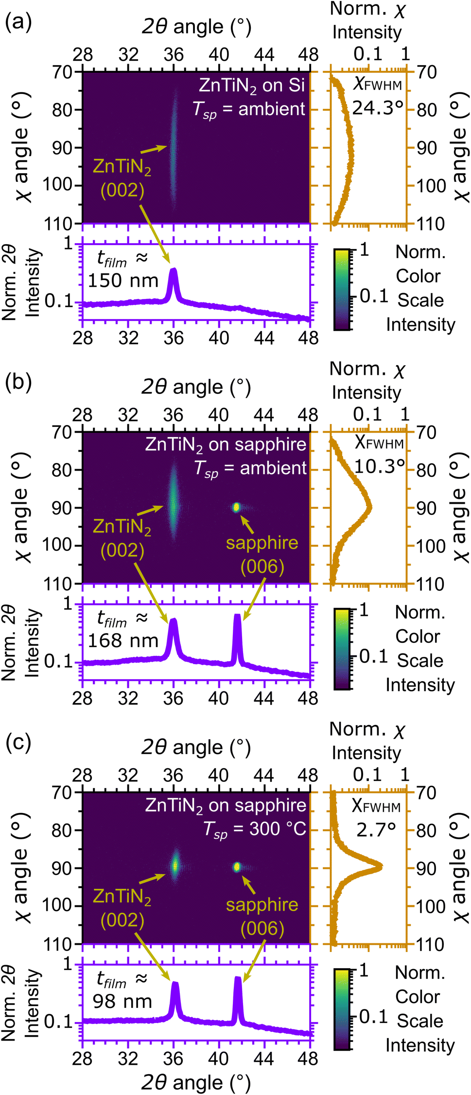 | ||
| Fig. 1 Two-dimensional (2θ and χ) X-ray diffraction of ZnTiN2 films grown on different substrates and at various growth temperature setpoints (Tsp): (a) ZnTiN2-AT-Si; (b) ZnTiN2-AT-sapph; and (c) ZnTiN2-300C-sapph. Integrated 1-dimensional plots are shown for each sample (below: intensity vs. 2θ; right: intensity vs. χ for the ZnTiN2 (002) peak), with intensity normalized across the sample set. Film thickness, tfilm, is reported for each. The ZnTiN2-AT-sapph film shows greater (002) texturing compared to the ZnTiN2-AT-Si film and the (002) orientation improves further when growth temperature is increased. | ||
Structural templating from the sapphire substrate provides a directed growth orientation that improves the alignment of the ZnTiN2 (002) crystallographic film texture. However, sputtering is a physical vapor deposition method and not all incoming atoms may have the necessary energy and/or time to migrate to the ideal surface sites needed for building a highly oriented single-crystal film.22 Increasing the substrate temperature can further improve film quality by enhancing the mobility of adatoms on the growth surface, leading to improved crystalline order in the growing film.19 This is clearly observed when increasing the growth temperature from ambient to a setpoint (Tsp) of 300 °C for ZnTiN2 deposition onto sapphire (hereafter referred to as “ZnTiN2-300C-sapph”). Films grown under these more energetic conditions maintain the (002) texture seen in previous films and the (002) peak is significantly narrower in χ (±5° from the surface normal, χFWHM = 2.7°) (Fig. 1c). The χ profile of the ZnTiN2-300C-sapph films nearly approaches that of the single crystal sapphire substrate on our diffractometer (±2° from the surface normal, χFWHM = 1.4°). ESI Fig. 1† shows 2D XRD plots across the entire measured 2θ and χ range for the three films shown in Fig. 1. A few films were also grown on sapphire at a higher Tsp of 450 °C and their film quality was only negligibly improved compared to those grown at Tsp of 300 °C. However, because the volatility of Zn is even more pronounced at Tsp = 450 °C, concerns about sample reproducibility led us to focus our efforts on films grown at Tsp = 300 °C. Films grown on non-templating Si at Tsp = 300 °C were polycrystalline with secondary phases and poor crystal quality (ESI Fig. 2†), indicating that a templating substrate is necessary to produce highly oriented ZnTiN2 films.
A subset of ZnTiN2-300C-sapph films were grown with a Sn-containing Zn target and contain approximately 12% Sn/(Sn + Zn + Ti) by XRF. An optimal Sn concentration for maximizing film quality was not explored in this work. However, the shared wurtzite crystal between ZnTiN2 and ZnSnN2 (ref. 16) should allow for fruitful investigations of isostructural alloying between these two systems. These Sn-containing films (hereafter referred to as “Sn:ZnTiN2-300C-sapph”) exhibit comparable crystalline quality by XRD to those grown without Sn, but show an average shift of the (002) peak to 1° lower 2θ values (a representative full area diffraction pattern is shown in ESI Fig. 3†). This shift is consistent with an expansion of the crystal lattice expected from Sn incorporation into the ZnTiN2 structure.16 While the difference in crystalline quality appears negligible by XRD, the Sn:ZnTiN2 films exhibit notable differences from the films that do not contain Sn, which will be described later.
2.2 Microstructural investigations by electron microscopy
Improvements in ZnTiN2 film crystalline quality with templating and high-temperature growth were also tracked by scanning electron microscopy (SEM) imaging. The ZnTiN2-AT-Si film exhibits a nanocrystalline, columnar-grained microstructure with a triangular faceted surface morphology as seen from both plan-view and cross-sectional SEM (Fig. 2a and b). This textured film morphology is seen quite commonly in sputtered nitride thin films22–26 and is consistent with our previous work.11 In contrast, the ZnTiN2-300C-sapph film exhibits a very homogeneous microstructure in both plan-view and cross-sectional SEM (Fig. 2c and d). The lack of distinct microstructural features is consistent with a marked improvement in crystalline quality. The Sn:ZnTiN2-300C-sapph films also exhibit the same high-quality homogeneous microstructure by SEM (ESI Fig. 4†).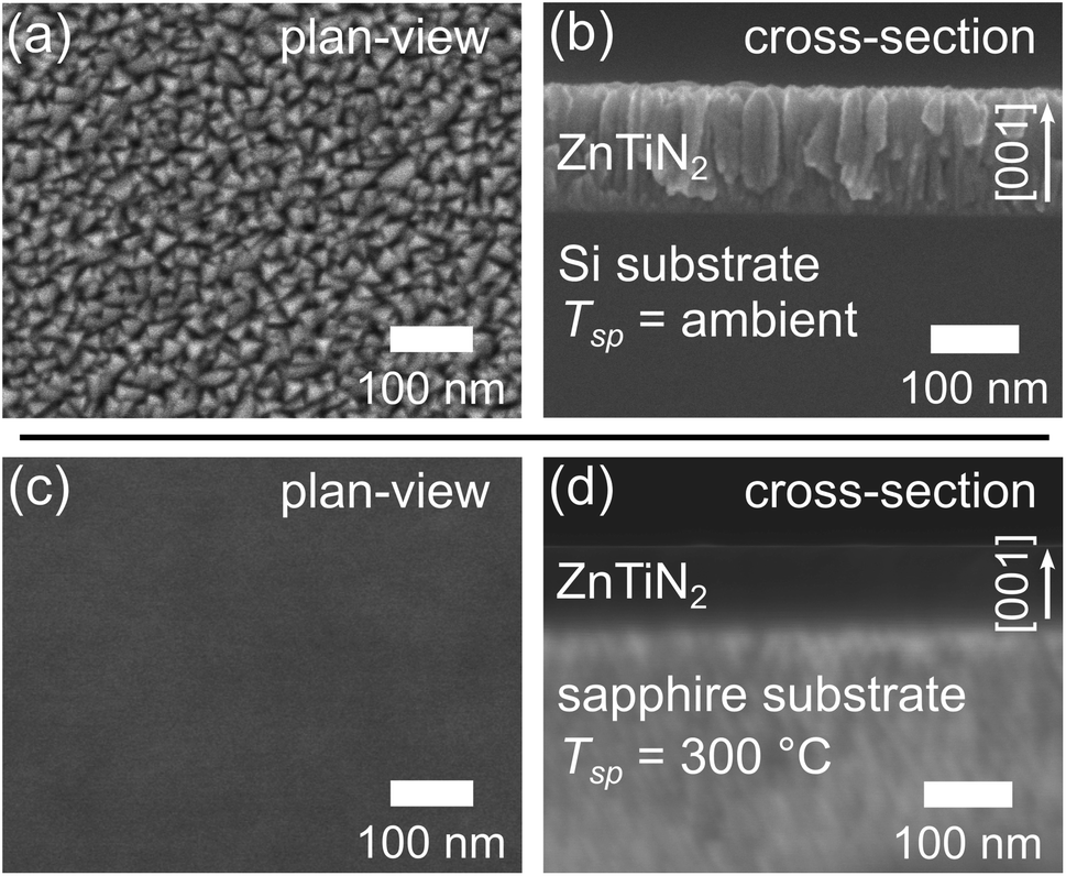 | ||
| Fig. 2 Representative (a and c) plan-view and (b and d) cross-sectional scanning electron microscopy micrographs from a ZnTiN2-AT-Si film (top) and a ZnTiN2-300C-sapph film (bottom). Ambient temperature growth on Si produces a polycrystalline (002)-textured columnar microstructure with a rough surface while growth on sapphire at elevated temperature results in a homogeneous and smooth ZnTiN2 film. | ||
While the improvement in crystal quality observed in SEM is remarkable, it cannot be quantified. Electron backscatter diffraction (EBSD) was used to further investigate the improvement in crystalline orientation with improved growth conditions, especially the in-plane orientation of ZnTiN2 that was not probed by XRD. Automated EBSD orientation maps could not be acquired on the ZnTiN2-300C-sapph films due to surface roughness (RRMS ≈ 3.00 nm, ESI Fig. 5a†), which was sufficiently high to obscure the electron backscatter diffraction patterns (EBSPs) and prevent software indexing. However, manually investigating the crystalline orientation by probing many locations across the film (>5000 μm2 area) showed an identically oriented electron backscatter diffraction pattern (EBSP) at every inspected point (a representative EBSP is shown in ESI Fig. 6†). Even though automated orientation maps could not be produced, this manual EBSD investigation along with the XRD and SEM indicates that the ZnTiN2 films grown on sapphire at elevated temperature are very uniformly oriented in all three crystallographic directions across the large areas that were examined.
Surprisingly, despite the similarities in XRD and SEM between films grown with and without Sn, the Sn:ZnTiN2-300C-sapph films exhibited very low surface roughness (RRMS ≈ 0.55 nm, ESI Fig. 5b†), affording clear EBSPs that can be automatically indexed to generate EBSD orientation maps. An inverse pole figure (IPF) map for the Z-axis (normal to the film surface) from a 78 μm × 63 μm region of a Sn:ZnTiN2-300C-sapph film (Fig. 3a) shows a completely homogeneous film oriented with the [001] direction parallel to the film growth direction. Corresponding X- and Y-axis IPF maps are shown in ESI Fig. 7,† confirming the homogeneous crystal orientation in-plane with respect to the film/substrate interface. A crystal model of ZnTiN2 in Fig. 3b indicates the crystal directions corresponding to the EBSD map axes. Multiple regions of similar size were measured on this film and showed the same uniform orientation. The average angular misorientation of each pixel with respect to its neighboring pixels (kernel averaged misorientation, KAM) is 0.35° ± 0.09°, confirming a very highly oriented film. The KAM of a commercial epi-ready GaN on sapphire template (3L Corporation) measured on this instrument is 0.18° ± 0.07°. The smoother surfaces of the Sn:ZnTiN2 films compared to the films grown without Sn are possibly explained by Sn acting as a surfactant, which has been observed in other nitride systems when supplying group IV elements (e.g., Si) during growth.20,21 Surfactants can promote 2-dimensional layer-by-layer growth, which has been shown to improve not only the surface quality, but also other material properties, of nitride thin films.27,28 A recent study has also demonstrated a flux-film-coated method to grow high quality AlN thin films using an Al–Sn flux, signifying a benefit of using low melting point elements or compounds for improving nitride thin film growth.29 However, the flux-film-coated method showed no significant concentration of Sn in the final AlN film which differs from the reactive sputtering method used in this work that shows Sn incorporated throughout the nitride film.
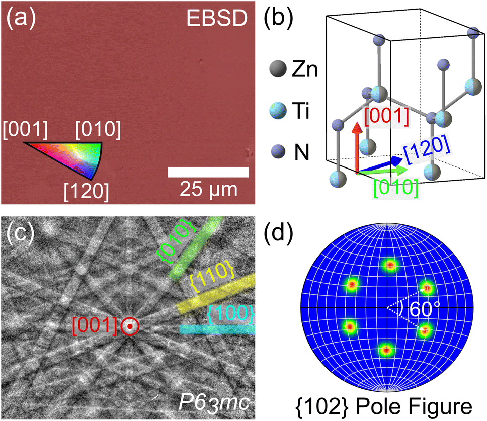 | ||
| Fig. 3 (a) EBSD inverse pole figure map from a Sn:ZnTiN2-300C-sapph film showing a homogeneous, (001)-oriented, single-crystal-like film. (b) The crystallographic directions of the color legend in (a) are shown schematically with respect to the wurtzite ZnTiN2 crystal structure. (c) Representative electron backscatter diffraction pattern from the Sn:ZnTiN2 film that is indexed to a wurtzite crystal structure (P63mc space group). Three low-index Kikuchi bands are highlighted. (d) {102} pole figure showing six-fold rotational symmetry of these off-growth-axis planes, confirming the biaxial orientation of the film. | ||
A representative electron backscatter diffraction pattern (EBSP) (Fig. 3c) from the Sn:ZnTiN2-300C-sapph film shows strong Kikuchi band intensities and is indexed to the wurtzite P63mc space group, as expected from the cation-disordered ZnTiN2 crystal structure. The same orientation indexed to P63mc was also observed in the EBSPs manually acquired from ZnTiN2 films grown without Sn. A {102} pole figure (Fig. 3d) further confirms the Sn:ZnTiN2-300C-sapph film is highly oriented in the planes off-axis from the growth direction; the pole figure exhibits six distinct peaks, separated by 60°, which clearly shows the six-fold rotational symmetry of the hexagonal wurtzite crystal structure. The combination of both in-plane and out-of-plane orientation (with respect to the growth direction) observed with EBSD across large areas confirms the biaxially-oriented nature of these “single-crystal-like” ZnTiN2 films grown with and without Sn on sapphire at elevated temperature.
2.3 Electronic transport properties
Electrical resistivity and Hall effect measurements were used to evaluate differences in the electronic transport properties of ZnTiN2 films grown on EXG glass and sapphire substrates, with and without Sn incorporation, at ambient and elevated growth temperatures (Table 1). The electrical resistivity for the films grown at Tsp = ambient were nearly identical; carrier concentrations and mobilities of films grown at Tsp = ambient could not be measured due to having Hall voltages below the measurement limit (<100 nV) of the Hall system. The ZnTiN2-300C-sapph film had a significantly lower resistivity compared to the ZnTiN2 films grown at ambient temperature, likely due to a combination of increased material quality and large n-type carrier concentration. The Sn:ZnTiN2-300C-sapph exhibited a resistivity slightly higher than the ZnTiN2-300C-sapph film but notably lower than the ZnTiN2 films grown at ambient temperature. This agrees with the observed improvements in material quality and its lower n-type carrier concentration compared to the ZnTiN2-300C-sapph film. Assuming a maximum mobility of 0.001 cm2 V−1 s−1, corresponding to the minimum measurement limit of the Hall system, we estimate a minimum carrier concentration of n ≈ 1021 cm−3 for the films grown at ambient temperature. Therefore, due to similar carrier concentrations across all ZnTiN2 films, the observed decrease in electrical resistivity of the films grown at elevated temperature can be at least partially attributed to their enhanced crystalline quality, most likely due to the elimination of grain boundary scattering because of their single-crystalline structure.| Sample | Resistivity (Ω cm) | Mobility (cm2 V−1 s−1) | Carrier concentration (cm−3) |
|---|---|---|---|
| ZnTiN2-AT-EXG | 3.89 ± 0.11 | <0.001 | ≈1021 |
| ZnTiN2-AT-sapph | 3.97 ± 0.10 | <0.001 | ≈1021 |
| ZnTiN2-300C-sapph | 0.123 ± 0.004 | (1.68 ± 0.036) × 10−2 | (3.01 ± 0.09) × 1021 |
| Sn:ZnTiN2-300C-sapph | 0.735 ± 0.006 | (4.58 ± 0.22) × 10−2 | (1.85 ± 0.01) × 1020 |
Carrier mobilities of 0.0168 cm2 V−1 s−1 and 0.0458 cm2 V−1 s−1 were measured for the ZnTiN2-300C-sapph and Sn:ZnTiN2-300C-sapph films, respectively. While these are not exceptional carrier mobilities relative to highly-developed nitride semiconductors (40–80 cm2 V−1 s−1 for GaN with n ≈ 1020 cm−3),30 they are comparable to, or even better than, oxide PEC electrode materials (0.044 cm2 V−1 s−1 for undoped BiVO4 and 0.008 cm2 V−1 s−1 for CuV2O6 with n ≈ 1018 cm−3)31,32 and indicates the success of our approach in improving the optoelectronic quality of the ZnTiN2 semiconductor. Additional efforts to reduce the carrier concentration in these films would likely further improve the carrier mobility.
2.4 Optical properties and photoexcited carrier kinetics
Spectroscopic ellipsometry was used to track changes in the optical properties of the ZnTiN2 films as a function of growth conditions. Plots of absorption coefficient versus photon energy were extracted from the modeled ellipsometry data (Fig. 4a). Baseline ZnTiN2-AT-Si films show an absorption onset near 2 eV, as expected from prior work.11 In these films, there is a relatively large amount of absorption present at photon energies in the “sub-gap” region, below 2 eV, compared to typical high-quality semiconductor materials that exhibit steep absorption onsets at their bandgap energy.33,34 High optical absorption in the sub-gap region is generally assumed to be associated with defect energy states that can arise from a variety of crystallographic defects or chemical impurities.35,36 Grain boundaries in polycrystalline films, as well as unintentional impurities such as oxygen contamination that was observed in our prior work,11 are likely culprits for high sub-gap optical absorption observed in the ZnTiN2 films grown on Si at ambient temperature. The ZnTiN2-AT-sapph film, which showed slightly better crystallinity by XRD (Fig. 1b), also show a slight improvement (that is, a decrease) in sub-gap absorption, although the difference is small.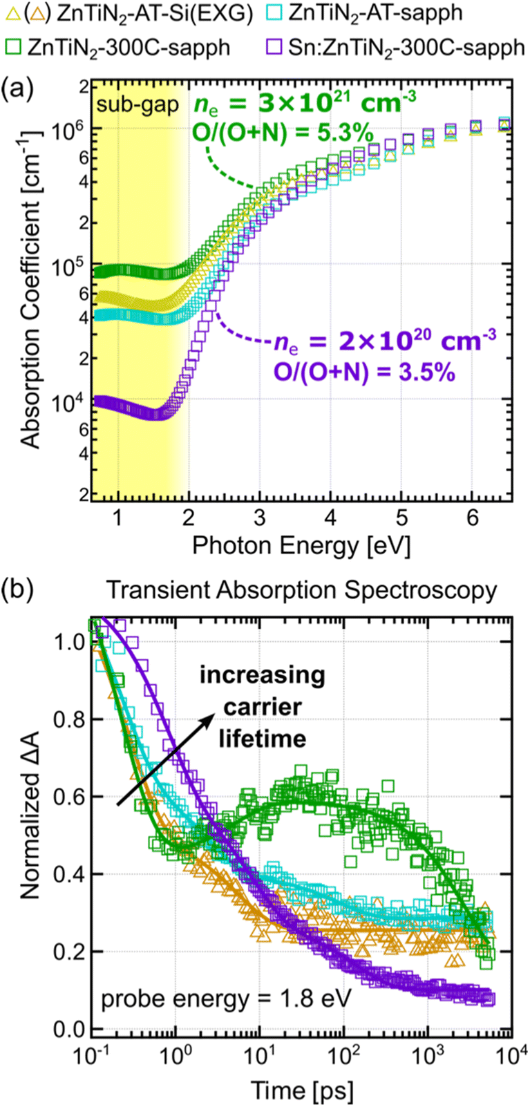 | ||
| Fig. 4 (a) Absorption coefficient vs. photon energy from spectroscopic ellipsometry for ZnTiN2 films grown with varying growth conditions. Higher optical quality is indicated by a decrease in the degree of sub-gap (≲2 eV) absorption. (b) Transient absorption kinetics of films grown with varying growth conditions at probe energies of 1.8 eV after photoexcitation at 3.1 eV. Normalized TA kinetic data are shown as markers and fits as solid lines. | ||
Increasing the growth temperature on sapphire substrates to Tsp of 300 °C resulted in an unexpected increase in sub-gap absorption in the ZnTiN2-300C-sapph film. In contrast, the Sn:ZnTiN2-300C-sapph film exhibits a dramatic decrease in sub-gap absorption, despite growth under nominally identical conditions. As shown from the Hall results, the ZnTiN2-300C-sapph film has an order of magnitude higher carrier density compared to its Sn:ZnTiN2 counterpart, which corroborates and could explain the large difference in free carrier absorption. Oxygen and carbon are common impurities unintentionally incorporated in nitride thin films that can introduce mid-gap defect states.37,38 Higher O and C contents are measured by X-ray photoelectron spectroscopy (XPS) depth profiling for the ZnTiN2-300C-sapph film (O/(O + N) = 5.3 ± 0.9%; C = 1.4 ± 0.4 at%) compared to the Sn:ZnTiN2-300C-sapph film (O/(O + N) = 3.5 ± 0.6%; C = 0.1 ± 0.2 at%). While this does agree with the trend observed in the Hall measurements, it does not fully account for the order of magnitude difference in carrier concentration between the two films and suggests a mechanism by which Sn may mitigate unintentional impurity incorporation and/or compensate n-type dopants in these films. The significant decrease in sub-gap absorption observed in the Sn:ZnTiN2-300C-sapph film compared to the other films analyzed is very likely due to a combined effect of having a lower impurity incorporation and carrier density as well as the single-crystal-like nature of these films (i.e., elimination of grain boundaries). For the highest optical quality Sn:ZnTiN2 films, a band gap of ∼1.8–2 eV is calculated from where the absorption coefficient curve crosses 104 cm−1.17,39
Transient absorption (TA) spectroscopy was used to assess the photoexcited carrier dynamics of the ZnTiN2 thin films produced in this study. Only ZnTiN2 films grown on EXG glass and sapphire substrates were probed using TA, as transmission-mode measurements are not possible on opaque Si substrates. Films grown at ambient temperature on EXG (ZnTiN2-AT-EXG) and Si (ZnTiN2-AT-Si) appear identical based on all methods used to characterize them. Full TA spectra are shown in ESI Fig. 8.† The spectra of all films exhibit similar characteristics after photoexcitation at 3.1 eV, including a broad photoinduced absorption spanning the visible regime with a distinct peak centered around 2.6 eV. Differences arise when monitoring the evolution of these features over time.
We monitored the kinetics of the films at a probe energy of 1.8 eV, near the lower energy edge of the spectra. The dynamics at 1.8 eV (Fig. 4b) show a rapid evolution within the first 1 ps following photoexcitation in all films. A qualitative comparison of decay rates within this region shows a similar trend to the optical sub-gap absorption trends, where lower optical quality is associated with faster decay kinetics. Rigorous TA analysis in the BiVO4 photoelectrode system has attributed these shorter ps timescale processes to excited carrier thermalization and defect-mediated fast electron–hole recombination.40 Loosely attributing these assignments to the ZnTiN2 system suggests that higher optical quality films exhibit longer photoexcited carriers lifetimes and less carrier recombination due to defect states, which are both important metrics to optimize for attaining high PEC device performance. From 1 ps onward, all films except for the ZnTiN2-300C-sapph film continue to exhibit kinetic decay signatures typical of photoexcited carrier thermalization and recombination in semiconductor materials. The ZnTiN2-300C-sapph film, however, shows a growth signature before starting to decay again around 30 ps. We attribute this unique growth feature to an increased population of excited carrier trapping in the ZnTiN2-300C-sapph film due to its significantly large carrier concentration as measured by Hall effect.
To further study the differences in carrier dynamics between synthesis conditions, transient absorption kinetics were also fit at a probe energy of 2.5 eV (ESI Fig. 9†) which is more sensitive to the kinetics of trapped charge carriers.40,41 Both films grown at ambient temperature display similar kinetic decay signatures at 2.5 eV and 1.8 eV probe energies, further indicating that excited carrier lifetime is dominated by fast electron–hole recombination in these films.40 In contrast, the films grown at elevated temperature show growth signatures from the 2.5 eV probe energy that plateau prior to decaying around the ns timescale. These kinetic signatures suggest a significantly larger degree of charge carrier trapping prior to recombination compared to films grown at ambient temperature. A possible explanation is the absence or lack of grain boundaries, which typically act as recombination sites, in the elevated temperature films (which are single-crystal-like) that allows trapping to become dominant at longer time scales. Further discussion and speculation of the TA kinetics fit at a 2.5 eV probe energy is provided in the ESI.† A more in-depth spectroscopic investigation would be required to quantitatively correlate TA kinetics to carrier concentration in ZnTiN2. However, the overall longer photoexcited carrier lifetimes observed for the Sn:ZnTiN2-300C-sapph film at both probe energies provide further evidence of its enhanced optoelectronic properties compared to the ZnTiN2 films without Sn.
2.5 Influence of Sn incorporation on electronic band structure
To gain additional understanding of the influence of Sn on the optoelectronic properties of ZnTiN2, we perform first-principles calculations based on density functional theory (DFT). Small concentrations of Sn are introduced into cation-ordered ZnTiN2, with Sn substituting for either Zn or Ti. We expect Sn to take up its more stable oxidation state of 4+ as commonly observed in Sn-containing sputtered nitride films,42–44 and so replacing Zn with Sn would be expected to effectively introduce two electrons, whereas Sn replacing Ti would be charge neutral. Our computed site-projected density of states (DOS) for a single Sn substitution (1.6% of cation sites) on Ti or Zn sites in 128-atom cation-ordered ZnTiN2 supercells (ESI Fig. 10†) indicates the DOS is mostly unchanged when Sn substitutes for Ti, while a deep gap state appears when Sn is substituted for Zn. This deep gap state contrasts with the optical absorption measurements that show the Sn:ZnTiN2-300C-sapph film exhibiting the lowest sub-gap optical absorption of all films studied, suggesting that Sn likely substitutes for Ti rather than Zn.However, DFT calculations of Sn substitution accounting for the cation-disordered structure of the ZnTiN2 films synthesized in this work are called for, as the cation disorder reduces the conduction band edge energies and increases valence band edge energies (leading to an overall reduction in band gap).11 Thus, we perform DFT calculations where we substitute Sn for Zn in a supercell that includes cation disorder (see ESI† for details of the supercell) and recompute the DOS and inverse participation ratio (IPR). In a cation-disordered supercell, each Zn and Ti has a different local atomic environment, a consequence of the disorder. We use DFT to compute the energetics of Sn substitution on Zn sites with different local environments and find the formation energy of the SnZn substitutional defect decreases for Zn sites with more Zn neighboring cations (i.e., it is easier to replace Zn with Sn in Zn clusters). For example, the SnZn formation energy for a Zn site with 8 Zn and 4 Ti neighbors is 55.1 meV per formula unit (f.u.) lower than that for a Zn site with 3 Zn and 9 Ti neighbors. This is consistent with our previous finding that Zn-rich regions or clusters are relatively energetically unfavorable.45 These calculations suggest that Sn incorporation, as well as enhanced growth kinetics at elevated growth temperatures, suppresses Zn clustering in the films, reducing the likelihood of fully Zn coordinated N motifs, which have been shown to introduce localized gap states,45 and promotes improved carrier transport and optical properties. In contrast, replacing Ti with Sn shows little variation, about 1.6 meV per f.u. for the sites we studied.
We compare the formation energies of SnZn and SnTi (ESI Fig. 11†), the relative difference between which originates from different total energies of one Zn- and Ti-replaced supercells and the chemical potentials of Zn and Ti, which depend on the synthesis conditions. Here we use the Zn–Ti–N phase diagram generated from Materials Project46,47 and DFT-PBE calculated energy of bulk metallic Zn and Ti, focusing on two extreme cases within the ZnTiN2 phase space where (1) the Zn chemical potential is at its lowest and Ti chemical potential is at its highest, and (2) the Ti chemical potential is at its highest and Zn is at its lowest. In the first case, except for the most energetically desirable SnZn defect where Sn replaces Zn with the most Zn neighbors, the formation energies of SnZn range from 14.6 to 58.8 meV per f.u. larger than SnTi formation energies. In the second case, all SnZn have at least 27.8 meV per f.u. larger formation energies than those of SnTi. Therefore, Sn is most likely to replace Ti sites and Zn sites within Zn clusters.
As shown previously, cation disorder introduces a local charge imbalance that broadens both valence and conduction bands.11,45 As the conduction band broadens, the gap state can merge into the conduction band and manifest as a shallow defect state. Fig. 5 shows density of states and inverse participation ratio, which quantifies the degree of localization of the wavefunction on each site at each energy, computed with DFT from three cation disordered supercells: one with no Sn substitution (Fig. 5a), one with all eight Sn substitutions on Ti sites (12.5% of cation sites) (Fig. 5b) and one with Sn replacing one Zn site with the most Zn neighbors and seven randomly selected Ti sites (Fig. 5c). The density of states of the two supercells with Sn are similar to that of the supercell without Sn. The highest occupied state of the supercell shown in Fig. 5c has mainly Ti d character, suggesting that SnZn is a shallow defect. Thus, our calculations demonstrate that energetically favorable SnZn and SnTi substitutional defects do not lead to mid-gap states in cation-disordered ZnTiN2, and we further hypothesize that Sn dopants help ameliorate severe local charge imbalance associated with Zn clustering and result principally in shallow defect levels.
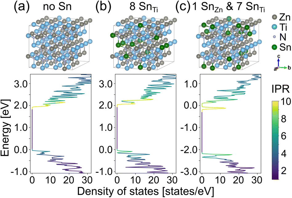 | ||
| Fig. 5 Projected density of states of cation-disordered ZnTiN2 supercells (a) without Sn incorporation, (b) with all eight Sn substitutions on Ti sites (12.5% of cation sites), and (c) with Sn replacing one Zn site with the most Zn neighbors and seven randomly selected Ti sites. The inverse participation ratio for all supercells is displayed on a color scale. The three DOS graphs have different energy limits resulting from the addition of 2e− to the supercell in (c), but the energy ranges are the same for comparison. | ||
3. Conclusions
In this work, we demonstrate heteroepitaxial growth of wurtzite-structured (cation-disordered) ZnTiN2, a promising photoelectrode material for PEC CO2R applications, on c-plane (001) sapphire substrates. By using lattice-matched substrates and depositing films at elevated temperature (300 °C), single-crystal-like films of ZnTiN2 are produced. Supplying Sn during growth on sapphire at elevated temperature reduces the surface roughness of the resulting Sn:ZnTiN2 film considerably. This suggests that Sn acts as a surfactant, possibly by promoting 2-dimensional layer-by-layer growth. Additionally, the Sn:ZnTiN2 films exhibited lesser amounts of O and C impurities and an order of magnitude lower n-type carrier concentration, implying a mechanism by which Sn decreases unintentional impurities and/or compensates n-type dopants in the growing film, resulting in enhanced optical absorption properties, carrier mobilities, and photoexcited carrier lifetimes compared to films grown under the same conditions without Sn. DFT calculations suggest that Sn substitution on energetically-favorable Zn and Ti cation sites in cation-disordered ZnTiN2 does not appreciably influence the optoelectronic properties and may even mitigate local charge imbalance in regions otherwise negatively impacted by Zn clustering. All these observations indicate an enhancement of charge carrier transport due to improvements in crystalline material quality, most notably the elimination of unintentional impurities and n-type point defects and grain boundaries in the single-crystal-like Sn:ZnTiN2 material.Overall, the optimization of ZnTiN2 thin film crystalline quality and associated improvements to optoelectronic properties demonstrated in this work are critical advances towards ZnTiN2 photoelectrodes with efficient photon absorption and photoexcited carrier extraction. An additional benefit of high-quality heteroepitaxial growth is the smoother film surface that enables more simplified development and characterization of electrochemically stable surface oxide layers. Studying and manipulating the interface between the ZnTiN2 film and these oxide layers, as well as the opposite interface with the substrate (and back contact layer in a device configuration), will be crucial for ensuring optimal electronic transport across the PEC device as a whole.48 Further improvements of these ZnTiN2 films should also focus on controlling various dopant types and their incorporation, to optimize carrier transport both within the ZnTiN2 films and between surrounding device layers. Future studies will also leverage the insights gained in this work to directly assess the performance and stability of ZnTiN2-based PEC devices under relevant electrochemical environments. In summary, a combination of these current and future efforts will be necessary for further optimizing the ZnTiN2 thin films for PEC applications.
4. Experimental methods
4.1 Synthesis
Thin films of Zn–Ti–N were deposited by radiofrequency co-sputtering in a custom vacuum chamber containing a cryoshroud surrounding the plasma zone. All films were deposited for 2 hours onto stationary substrates to create a lateral compositional gradient across the sample or onto rotating substrates once deposition conditions were well-defined. A combination of Zn, Ti, and alloy ZnTi targets (all 2′′ diameter) were used to allow for compositional flexibility throughout the film optimization process due to the dissimilar temperature-dependent sputtering rates of Zn and Ti. A Zn target containing approximately 5 atom% Sn, measured by XRF, was used for depositing the Sn-containing ZnTiN2 films. RF power densities on each target were tuned at each set of growth conditions such that samples containing nominally stoichiometric films with one-to-one Zn![[thin space (1/6-em)]](https://www.rsc.org/images/entities/char_2009.gif) :Ti ratios were produced. Specific growth conditions and target powers are reported in ESI Table 1.† Substrates used in this work were either single-side-polished (001)-oriented silicon with native oxide, Corning EXG glass, or double-side-polished (001)-oriented Al2O3 (sapphire). For all depositions, a chamber base pressure < 4 × 10⁻⁷ torr was reached prior to flowing 20 sccm of Ar and 10 sccm of N2 while maintaining a chamber pressure of 3.5 × 10⁻³ torr by controlling a partially closed gate valve to the turbomolecular pump. The deposition temperature was either left at ambient or increased using a UV lamp to heat the Inconel platen from the backside, thereby heating the substrate which is in direct thermal contact with the front of the platen. Growth temperatures were chosen and reported based on the heater setpoint (Tsp), which was calibrated using a thermocouple to measure the temperature at the center of the front-side of the platen where the substrate is held and does not account for unintentional heating from the RF sputtering process. The actual temperature at the substrate/growth surface was not measured.
:Ti ratios were produced. Specific growth conditions and target powers are reported in ESI Table 1.† Substrates used in this work were either single-side-polished (001)-oriented silicon with native oxide, Corning EXG glass, or double-side-polished (001)-oriented Al2O3 (sapphire). For all depositions, a chamber base pressure < 4 × 10⁻⁷ torr was reached prior to flowing 20 sccm of Ar and 10 sccm of N2 while maintaining a chamber pressure of 3.5 × 10⁻³ torr by controlling a partially closed gate valve to the turbomolecular pump. The deposition temperature was either left at ambient or increased using a UV lamp to heat the Inconel platen from the backside, thereby heating the substrate which is in direct thermal contact with the front of the platen. Growth temperatures were chosen and reported based on the heater setpoint (Tsp), which was calibrated using a thermocouple to measure the temperature at the center of the front-side of the platen where the substrate is held and does not account for unintentional heating from the RF sputtering process. The actual temperature at the substrate/growth surface was not measured.
4.2 Characterization
Cation composition was analyzed with a Fischer XDV-SDD X-ray fluorescence spectrometer to measure the lateral compositional gradients across the sample using an automated mapping routine and to locate sample positions containing the desired stoichiometric ZnTiN2 composition. Quantification routines for cation composition in XRF were calibrated using compositional data acquired from Rutherford backscattering spectrometry.11A Bruker D8 Discover equipped with an area detector was used to collect 2-dimensional X-ray diffraction plots at each sample position using an automated mapping routine. 2D XRD spectra were acquired over a range of 2θ = 19–52° and χ = 60–120° using Cu Kα radiation. 2D XRD plots covering the entire 2θ range are shown in ESI Fig. 1.† Integrated 1-dimensional XRD plots were calculated by integrating over the entire χ range to get intensity versus 2θ and by integrating over just the 2θ range containing the ZnTiN2 (002) diffraction peak (ca. 34–37°) to get intensity versus χ.
Scanning electron microscopy was performed using either a Hitachi S-4800 or FEI Nova NanoSEM 630 operating at 3 kV accelerating voltage and a working distance of 3–5 mm. Electron backscatter diffraction was conducted using an Oxford Symmetry detector and Aztec software on the FEI Nova NanoSEM 630 operating at a 20 kV accelerating voltage and 12 nA beam current. A resolution of 1024 × 896 pixels with 83.4 nm pixel size was used for mapping. The mean angular deviation between the measured diffraction patterns and simulated reference wurtzite crystal structure was 0.68° ± 0.09°. All films studied in this work were thicker than 100 nm, which is greater than the typically cited upper limit on information depth in EBSD (around 50 nm),49 ensuring that EBSD data were acquired only from the film and not the underlying substrate.
Spectroscopic ellipsometry data were acquired using a J. A. Woollam Co. M-2000 variable angle ellipsometer at incident angles of 65°, 70°, and 75° over a photon energy range of 0.73–6.46 eV. Raw Ψ and Δ data were modeled and fit using the CompleteEASE software (version 6.63) to extract optical parameters n, k, and absorption coefficient. A generalized oscillator model was constructed using a PSemi-M0 oscillator to fit the ZnTiN2 optical absorption edge and a single Drude oscillator to fit the sub-gap free carrier absorption region below 2 eV.
Resistivity and Hall effect measurements were done at ambient temperature on a LakeShore FastHall system in a van der Pauw geometry using indium contacts soldered onto the corners of 10 mm × 10 mm square pieces cleaved from the larger sample.
XPS measurements were conducted on a customized Physical Electronics VersaProbe III using monochromatic Al Kα radiation. Analysis conditions include a pass energy of 140 eV and close-to-normal photoelectron take-off angle of 85°. Depth profiling was performed with a gas cluster ion source (15 kV Ar2000+). In some cases, dual electron beam and low energy ion beam neutralization was used to compensate for charging of resistive samples. Atomic concentrations were derived from default sensitivity factors in the analysis software MultiPak v9.6.1.7. Average values for O/(O + N)% and C at% were calculated for the ZnTiN2-300C-sapph and Sn:ZnTiN2-300C-sapph films from the region of the XPS depth profile where the elemental composition remained consistent (see ESI Fig. 12†) to account for any oxygen infiltration between the time of synthesis and XPS measurements. All films were stored in a desiccator under a N2 atmosphere.
Transient absorption spectroscopy data were collected using a Coherent Libra Ti:sapphire laser (1 kHz, 800 nm (1.55 eV) fundamental, 150 fs pulse width). The 3.1 eV (400 nm, 500–1200 nJ per pulse) pump pulse was generated in a TOPAS-C optical parametric amplifier and the white light probe pulses were produced via supercontinuum generation in a thin sapphire window (λprobe = 2.8–1.55 eV). A mechanical delay stage was used to delay the probe relative to the pump, and pump and probe were spatially overlapped at the sample. A portion of the probe was picked off before the sample to reduce noise to <0.1 mOD. A fiber-optic coupled multichannel spectrometer with a CMOS sensor was used to monitor changes in the probe. Helios software from Ultrafast Systems was used to collect the data and the data were chirp corrected and analyzed with either Ultrafast Systems' SurfaceXplorer software or custom chirp correction code in Igor PRO and fit using the lmfit Python package.
DFT calculations were performed with the Vienna Ab Initio Simulation Package (VASP) and projector augmented wave (PAW) potentials, treating 3d2 4s2, 3d10 4s2, and 2s2 2p3 electrons explicitly for Ti, Zn, and N, respectively. We used the exchange–correlation functional of Perdew, Burke, and Ernzerhof (PBE)41 to compute total energies, Hellmann–Feynman forces, and optimize the atomic structure. The internal coordinates were relaxed while lattice parameters were fixed. An energy cutoff of 600 eV was used and total energies were converged to within 10−7 eV per atom and all Hellmann–Feynman forces are below 0.01 eV Å−1 on each atom. For our electronic structure calculations, we used a Heyd–Scuseria–Ernzerhof (HSE06) screened hybrid functional. Our supercells contained 128 atoms (32 f.u.). For PBE calculations, a Γ-centered 4 × 4 × 4 k-mesh was used; for hybrid calculations, a Γ-centered 2 × 2 × 2 k-mesh was used. Gaussian smearing was used in our Brillouin zone integrations, with a smearing parameter of 0.02 eV in all calculations. These computations are performed without considering the presence of oxygen.
Author contributions
This project was jointly conceived of by A. L. G., J. S. M. and A. Z. J. S. M. synthesized the ZnTiN2 films and characterized them by all experimental techniques with the exception of transient absorption spectroscopy, which was performed by M. K. G. and E. K. R., and X-ray photoelectron spectroscopy, which was performed by C. L. P. S. K. and J. B. N. carried out theoretical electronic structure calculations. A. L. G., A. Z. and J. B. N. were responsible for funding acquisition and project management. J. S. M. wrote the manuscript and designed the figures with assistance and feedback from all other authors.Conflicts of interest
J. S. M., A. Z., and A. L. G. are currently submitting a record of invention based on this work and the results reported in this manuscript.Acknowledgements
We acknowledge Goutam Paul for conducting atomic force microscopy measurements. We acknowledge Angel Garcia-Esparza and Junko Yano for insightful discussions. This work was performed at the National Renewable Energy Laboratory, operated by Alliance for Sustainable Energy, LLC, for the U.S. Department of Energy (DOE) under contract no. DE-AC36-08GO28308. This material is based on work performed by the Liquid Sunlight Alliance, which is supported by the U.S. Department of Energy, Office of Science, Office of Basic Energy Sciences, Fuels from Sunlight Hub under award number DE-SC0021266. We acknowledge computational resources provided by the National Energy Research Scientific Computing Center (NERSC), supported by the Office of Science of the Department of Energy operated under contract no. DE-AC02-05CH11231. The views expressed in the article do not necessarily represent the views of the DOE or the U.S. Government.References
- A. C. Nielander, M. R. Shaner, K. M. Papadantonakis, S. A. Francis and N. S. Lewis, Energy Environ. Sci., 2014, 8, 16–25 RSC.
- A. K. Singh, J. H. Montoya, J. M. Gregoire and K. A. Persson, Nat. Commun., 2019, 10, 443 CrossRef CAS PubMed.
- M. G. Kast, L. J. Enman, N. J. Gurnon, A. Nadarajah and S. W. Boettcher, ACS Appl. Mater. Interfaces, 2014, 6, 22830–22837 CrossRef CAS PubMed.
- M. Ben-Naim, R. J. Britto, C. W. Aldridge, R. Mow, M. A. Steiner, A. C. Nielander, L. A. King, D. J. Friedman, T. G. Deutsch, J. L. Young and T. F. Jaramillo, ACS Energy Lett., 2020, 5, 2631–2640 CrossRef CAS.
- R. Liu, Z. Zheng, J. Spurgeon and X. Yang, Energy Environ. Sci., 2014, 7, 2504–2517 RSC.
- Y. W. Chen, J. D. Prange, S. Dühnen, Y. Park, M. Gunji, C. E. D. Chidsey and P. C. McIntyre, Nat. Mater., 2011, 10, 539–544 CrossRef CAS PubMed.
- S. Hu, M. R. Shaner, J. A. Beardslee, M. Lichterman, B. S. Brunschwig and N. S. Lewis, Science, 2014, 344, 1005–1009 CrossRef CAS PubMed.
- F.-R. F. Fan, B. L. Wheeler, A. J. Bard and R. N. Noufi, J. Electrochem. Soc., 1981, 128, 2042 CrossRef CAS.
- S. Hu, N. S. Lewis, J. W. Ager, J. Yang, J. R. McKone and N. C. Strandwitz, J. Phys. Chem. C, 2015, 119, 24201–24228 CrossRef CAS.
- J. Chi, Z. Jiang, J. Yan, A. Larimi, Z. Wang, L. Wang and W. Shangguan, Mater. Today Chem., 2022, 26, 101060 CrossRef CAS.
- A. L. Greenaway, S. Ke, T. Culman, K. R. Talley, J. S. Mangum, K. N. Heinselman, R. S. Kingsbury, R. W. Smaha, M. K. Gish, E. M. Miller, K. A. Persson, J. M. Gregoire, S. R. Bauers, J. B. Neaton, A. C. Tamboli and A. Zakutayev, J. Am. Chem. Soc., 2022, 144, 13673–13687 CrossRef CAS PubMed.
- C. Tholander, C. B. A. Andersson, R. Armiento, F. Tasnádi and B. Alling, J. Appl. Phys., 2016, 120, 225102 CrossRef.
- K. A. Persson, B. Waldwick, P. Lazic and G. Ceder, Phys. Rev. B: Condens. Matter Mater. Phys., 2012, 85, 235438 CrossRef.
- A. K. Singh, L. Zhou, A. Shinde, S. K. Suram, J. H. Montoya, D. Winston, J. M. Gregoire and K. A. Persson, Chem. Mater., 2017, 29, 10159–10167 CrossRef CAS.
- Y. Hinuma, T. Hatakeyama, Y. Kumagai, L. A. Burton, H. Sato, Y. Muraba, S. Iimura, H. Hiramatsu, I. Tanaka, H. Hosono and F. Oba, Nat. Commun., 2016, 7, 11962 CrossRef CAS PubMed.
- I. S. Khan, K. N. Heinselman and A. Zakutayev, J. Phys.: Energy, 2020, 2, 032007 CAS.
- R. R. Schnepf, J. J. Cordell, M. B. Tellekamp, C. L. Melamed, A. L. Greenaway, A. Mis, G. L. Brennecka, S. Christensen, G. J. Tucker, E. S. Toberer, S. Lany and A. C. Tamboli, ACS Energy Lett., 2020, 5, 2027–2041 CrossRef CAS.
- L. Liu and J. H. Edgar, Mater. Sci. Eng., R, 2002, 37, 61–127 CrossRef.
- K. Reichelt and X. Jiang, Thin Solid Films, 1990, 191, 91–126 CrossRef.
- V. Lebedev, F. M. Morales, H. Romanus, S. Krischok, G. Ecke, V. Cimalla, M. Himmerlich, T. Stauden, D. Cengher and O. Ambacher, J. Appl. Phys., 2005, 98, 093508 CrossRef.
- S. Tanaka, S. Iwai and Y. Aoyagi, Appl. Phys. Lett., 1996, 69, 4096–4098 CrossRef CAS.
- S. Mahieu, P. Ghekiere, D. Depla and R. De Gryse, Thin Solid Films, 2006, 515, 1229–1249 CrossRef CAS.
- S. Mahieu, G. Buyle, P. Ghekiere, S. Heirwegh, R. De Gryse and D. Depla, Thin Solid Films, 2006, 515, 416–420 CrossRef CAS.
- D. Drury, K. Yazawa, A. Mis, K. Talley, A. Zakutayev and G. L. Brennecka, Phys. Status Solidi RRL, 2021, 15, 2100043 CrossRef CAS.
- N. Beddelem, S. Bruyère, F. Cleymand, S. Diliberto, C. Longeaud, S. le Gall, R. Templier, P. Miska and B. Hyot, Thin Solid Films, 2020, 709, 138192 CrossRef CAS.
- M. A. Signore, D. Valerini, A. Rizzo, L. Tapfer, L. Capodieci and A. Cappello, J. Phys. D: Appl. Phys., 2010, 43, 225401 CrossRef.
- M. Hermann, F. Furtmayr, F. M. Morales, O. Ambacher, M. Stutzmann and M. Eickhoff, J. Appl. Phys., 2006, 100, 113531 CrossRef.
- G. Nishio, S. Yang, H. Miyake and K. Hiramatsu, J. Cryst. Growth, 2013, 370, 74–77 CrossRef CAS.
- Y. Song, F. Kawamura, K. Shimamura, T. Ohgaki and N. Ohashi, AIP Adv., 2020, 10, 115011 CrossRef CAS.
- T. T. Mnatsakanov, M. E. Levinshtein, L. I. Pomortseva, S. N. Yurkov, G. S. Simin and M. Asif Khan, Solid-State Electron., 2003, 47, 111–115 CrossRef CAS.
- F. F. Abdi, T. J. Savenije, M. M. May, B. Dam and R. van de Krol, J. Phys. Chem. Lett., 2013, 4, 2752–2757 CrossRef CAS.
- A. Song, S. Liu, Q. Wang, D. Gao and J. Hu, J. Environ. Chem. Eng., 2023, 11, 109892 CrossRef CAS.
- J. F. Muth, J. D. Brown, M. a. L. Johnson, Z. Yu, R. M. Kolbas, J. W. Cook and J. F. Schetzina, MRS Internet J. Nitride Semicond. Res., 1999, 4, 502–507 CrossRef.
- A. R. Zanatta, Sci. Rep., 2019, 9, 11225 CrossRef CAS PubMed.
- S. Suihkonen, S. Pimputkar, S. Sintonen and F. Tuomisto, Adv. Electron. Mater., 2017, 3, 1600496 CrossRef.
- S. Pimputkar, S. Suihkonen, M. Imade, Y. Mori, J. S. Speck and S. Nakamura, J. Cryst. Growth, 2015, 432, 49–53 CrossRef CAS.
- G. A. Slack, L. J. Schowalter, D. Morelli and J. A. Freitas, J. Cryst. Growth, 2002, 246, 287–298 CrossRef CAS.
- J. L. Lyons, A. Janotti and C. G. Van de Walle, Phys. Rev. B: Condens. Matter Mater. Phys., 2014, 89, 035204 CrossRef.
- C. L. Melamed, J. Pan, A. Mis, K. Heinselman, R. R. Schnepf, R. Woods-Robinson, J. J. Cordell, S. Lany, E. S. Toberer and A. C. Tamboli, J. Mater. Chem. C, 2020, 8, 8736–8746 RSC.
- J. Ravensbergen, F. F. Abdi, J. H. van Santen, R. N. Frese, B. Dam, R. van de Krol and J. T. M. Kennis, J. Phys. Chem. C, 2014, 118, 27793–27800 CrossRef CAS.
- T. Yoshihara, R. Katoh, A. Furube, Y. Tamaki, M. Murai, K. Hara, S. Murata, H. Arakawa and M. Tachiya, J. Phys. Chem. B, 2004, 108, 3817–3823 CrossRef CAS.
- D. Lützenkirchen-Hecht and R. Frahm, Thin Solid Films, 2005, 493, 67–76 CrossRef.
- C. M. Caskey, J. A. Seabold, V. Stevanović, M. Ma, W. A. Smith, D. S. Ginley, N. R. Neale, R. M. Richards, S. Lany and A. Zakutayev, J. Mater. Chem. C, 2015, 3, 1389–1396 RSC.
- K. k. Chinnakutti, L. Patra, V. Panneerselvam, D. Govindarajan, S. Kheawhom, J. Theerthagiri, Y. Yu, S. T. Salammal and M. Y. Choi, Mater. Today Chem., 2022, 25, 100957 CrossRef CAS.
- S. Ke, J. S. Mangum, A. Zakutayev, A. L. Greenaway and J. B. Neaton, Chem. Mater., 2023 Search PubMed.
- A. Jain, S. P. Ong, G. Hautier, W. Chen, W. D. Richards, S. Dacek, S. Cholia, D. Gunter, D. Skinner, G. Ceder and K. A. Persson, APL Mater., 2013, 1, 011002 CrossRef.
- S. P. Ong, L. Wang, B. Kang and G. Ceder, Chem. Mater., 2008, 20, 1798–1807 CrossRef CAS.
- R. R. Prabhakar, R. Lemerle, M. Barecka, M. Kim, S. Seo, E. N. Dayi, I. D. Tos and J. W. Ager, J. Mater. Chem. A, 2023, 11, 13588–13599 RSC.
- W. Wisniewski and C. Rüssel, Scanning, 2016, 38, 164–171 CrossRef CAS PubMed.
Footnote |
| † Electronic supplementary information (ESI) available. See DOI: https://doi.org/10.1039/d3ta06200g |
| This journal is © The Royal Society of Chemistry 2024 |