
Prebaking of an SnS source with sulfur for achieving higher photovoltaic performance in VTD-SnS thin films for solar cells†
Rahul Kumar
Yadav
 ,
Pravin S.
Pawar
,
Yong Tae
Kim
,
Indu
Sharma
and
Jaeyeong
Heo
*
,
Pravin S.
Pawar
,
Yong Tae
Kim
,
Indu
Sharma
and
Jaeyeong
Heo
*
Department of Materials Science and Engineering, and Optoelectronics Convergence Research Center, Chonnam National University, Gwangju 61186, Republic of Korea. E-mail: jheo@jnu.ac.kr
First published on 15th January 2024
Abstract
Given its preeminent photovoltaic properties, tin sulfide (SnS) has attracted remarkable interest and has been explored as an absorber for thin-film solar cells in the last few decades. However, the power conversion efficiency (PCE) of SnS-based solar cells is typically below 4%. The deficit in open circuit voltage (VOC) of devices with shunt losses can be reduced by altering the sulfur vacancy and surface roughness of the vapor transport deposition (VTD)-SnS absorber. Therefore, this paper reports an effective approach to strengthen the efficiency of the VTD-SnS device by reducing the sulfur vacancy (VS). To this end, the SnS source was prebaked with a very small amount of sulfur powder in the same tube before the absorber layer deposition, and the efficiency of the fabricated VTD-SnS solar cell increased from 3.39 to 4.82%. This improvement was attributed to the reduction in the VS and the improved surface profile of the film. The reduction in the VS resulted in a decrease in the bulk defects, thus enhancing the collection of generated charge carriers. Additionally, the dark current of the prebaked source device reduced, indicating the improved shunt properties of the prebaked film; nevertheless, the shunt properties can be further enhanced by improving the interfacial properties and surface roughness of the film.
1. Introduction
Photovoltaic (PV) technology is a favorable, widely recognized, and promising candidate for meeting future energy demands.1,2 Thin-film PVs, which are lightweight and require a minimal absorber material, are suitable for wide-area applications. Currently, thin-film solar cells (TFSCs) with absorbers, such as CIGS, CdTe, and GaAs, have achieved a power conversion efficiency (PCE) of >22%.2–4 However, the scarcity and toxicity of the constituent elements in absorber materials, as well as the severe loss in the open circuit voltage (VOC), have restricted their wide area application. Recently, novel absorber materials with less toxic and earth-abundant constituents, such as Sb2Se3, Sb2S3, Cu2ZnSn(S,Se)4, SnS, SnSe, and GeSe, have attracted tremendous attention.5–9The binary chalcogenide SnS is an auspicious material for preparing absorbers for PV applications owing to its earth-abundance, low-cost, and non-toxic constituents. Additionally, SnS thin films exhibit an optimal bandgap of 1.1 to 1.4 eV, which is appropriate for PV applications with a high light absorption coefficient (>104 cm−1).10,11 Different deposition techniques (such as vapor transport deposition (VTD), atomic layer deposition (ALD), thermal evaporation (TE), sputtering, and chemical synthesis) have been employed for the preparation of stoichiometric, pure-phase, and single-phase SnS films.11–14 However, regardless of favorable material properties, the PCE of SnS absorber-based PVs is significantly below its Shockley–Queisser efficiency limit. To date, the efficiency of SnS absorber-based TFSCs with a superstrate configuration is 4.8% (uncertified),15 and the PCE in a substrate configuration is 4.36% (certified).11,16 This low performance can be attributed to the unmatched band alignment, poor material quality (e.g., defects and secondary phases), and less optimized configuration.13 Particularly, the low performance of SnS absorber-based TFSCs can be mainly attributed to the VOC deficit and loss in the short circuit current density (JSC).17 The surface roughness of the absorber film plays a crucial role in heterojunctions and controls the deposition of the buffer layer in the substrate configuration. Previous studies have significantly enhanced the VOC by passivating the top surface of the ALD-grown SnS absorber layer with 1 nm SnO2 in the substrate configuration and with a Zn(O,S) buffer layer.11,16,18 Although the ALD-grown SnS-based TFSCs exhibited improved performance and surpassed the 4% PCE limit, the slow growth rate and small-scale sample size have limited the further use of ALD. Recently, a study reported the improved performance of spin-coated FTO/nano-structured TiO2/SnS/top contact-Au with a superstrate configuration by the additional treatment of the absorber surface with SnCl2, and the improved performance was attributed to the uniformity and densely packed top surface morphology.15 Although few studies have reported an efficiency of above 4% for SnS absorber-based TFSCs, fabricating SnS absorber-based TFSCs with an efficiency of above 4% is challenging.13
Cadmium sulfide (CdS), grown by chemical bath deposition (CBD), is the most extensively used n-type buffer layer for the small (laboratory)- and large (industry)-scale fabrication of TFSCs. Studies have investigated the heterojunction of CBD-CdS with SnS thin films deposited by different techniques (e.g., VTD, ALD, TE, CBD, spin coating, and sputtering). It is well known that VTD is a rapid, low cost, scalable, and successfully commercialized thin-film deposition technique. Thin films deposited using VTD exhibit compact morphology and good crystallinity. In a previous study, we demonstrated a certified efficiency of 4.225% (4.36% uncertified in a house installed solar simulator)19 for a VTD-grown absorber with a CBD-CdS buffer layer by improving the heterojunction interface quality. To achieve this, the substrate temperature and duration for sputtering the window layer (aluminum-doped zinc oxide (AZO)) were optimized. Additionally, intrinsic zinc oxide (i-ZnO) film was modified to achieve improved results.20 SnS/CdS heterojunction TFSCs, with an absorber thickness of ∼1.3 μm, were prepared using VTD, and the device achieved a maximum PCE of 4.36%.19
In this study, a VTD-deposited SnS (prebaked with sulfur) thin film absorber and CBD-CdS buffer layer were used to fabricate TFSCs with a substrate structure, and the device achieved a maximum PCE of 4.82%. The performance of the device was improved by prebaking the SnS source with a small amount of sulfur before deposition. Additionally, the prebaking temperature and time of the SnS source were optimized before deposition. The study of the PV properties and diode quality, dark J–V measurement, and external quantum efficiency (EQE) were examined. The top surface roughness was analyzed using atomic force microscopy (AFM). The prebaked “SnS + S” source device was compared with the reference device (without prebaked (W.B.) SnS source). This study reports an uncertified efficiency of 4.82% with a highest JSC of 25.87 mA cm−2 and provides a road map to achieve a PCE of above 5%.
2. Experimental section
Prebaking of the SnS source with sulfur
First, 0.32 g of SnS source (5 N pure, iTASCO) and 0.015 g of sulfur flakes (5 N pure, Sigma-Aldrich) were manually added into a boat-shaped ceramic pot, and the pot was placed at the center of the VTD (S&R Korea, SRDVF-LV-3B-1608) heating area. Before the deposition of the thin film, the (SnS + S) source prebaked in the VTD furnace at various temperatures from 550 to 700 °C. The VTD furnace was pumped down to 5 mTorr using a rotary pump before starting the process. The ramping rate of the temperature was fixed at 20 °C per min to increase the temperature of the furnace to the set temperature and the furnace was allowed to stand stable at the set temperature for 20 min. Afterward the power was turned off and the furnace was cooled naturally to room temperature. The Ar gas was supplied throughout the prebaking process to sustain a steady pressure of 2 Torr. In the next step, the substrate holder with the substrate was inserted in the furnace for film deposition. Furthermore, to optimize the prebaking time, the (SnS + S) source was prebaked for various times from 15 to 45 min at an optimized temperature of 600 °C with the same ramping rate of temperature and pressure inside the tube. The substrate holder temperature was ∼450 °C. We observed that the evaporated vapor was deposited at the wall of the tube and during the second time deposition a small amount of material deposited at the wall was redeposited at the substrate.Thin film deposition
Molybdenum (Mo) deposited on soda lime glass (SLG) with a thickness of ∼1 μm and sheet resistance of 150 mΩ □−1 was taken as the substrate, after which the substrate was diced into smaller sections with a dimension of 2.5 cm × 2.5 cm. Thereafter, the substrates were sequentially rinsed with isopropyl alcohol (IPA) and deionized water for 20 min each in an ultrasonic bath, after which they were dehydrated in a N2 gas flow and then seal packed. For the deposition of the SnS thin film, a one zone VTD furnace was deployed, which was used for prebaking the SnS source. After prebaking of (SnS + S) and cooling down to room temperature, the furnace was vented using N2 gas, and the substrate placed at a flat quartz holder was inserted at one end of the heating area of the VTD. Thereafter, the pressure inside the furnace was pumped down again to 5 mTorr. Subsequently, the VTD furnace was pressurized at 2 Torr with argon gas, and it was maintained throughout the process. The VTD furnace was heated to 600 °C at a heating rate of 20 °C, and the temperature (600 °C) was held for 25 min at a steady furnace pressure. The deposition time was fixed at 25 min in each case. After completing the growth process, the furnace was cooled naturally at room temperature, and the samples were used to fabricate TFSCs, and were characterized. After the deposition of each sample, the furnace tube was cleaned using IPA and baked for 60 min at a temperature of 700 °C and an Ar flow of 160 sccm to remove the material deposited at the wall of the tube to avoid contamination.Device fabrication
After the SnS thin-film deposition, the samples were used to deposit a CdS n-type buffer layer to prepare the heterojunction using the conventional CBD method. Briefly, the chemicals were mixed in a bath at 8 °C, after which the n-CdS layer was deposited in a circulating bath at 60 °C for 22 min. Thereafter, ∼50 nm i-ZnO and 350 nm AZO layers were deposited using radio frequency sputtering. The finger top contact of Al was deposited using DC sputtering, and a final device structure of SLG/Mo/VTD-SnS/CBD-CdS/i-ZnO/AZO/Al was achieved and termed as the prebaked SnS source device. The devices were divided into six cells with a cell area of 0.36 cm2 using pattern masking, including a top metal strip area of 0.06 cm2.We have prepared a set of devices without the prebaking conditions (discussed in the prebaking section) for reference. The device is termed as without prebaked (W.B.) source device.
Characterization of the film and device
The crystallinity of Mo/SnS thin film deposited using VTD was analyzed using X-ray diffraction (XRD) with a Cu Kα radiation source with a wavelength of 1.542 Å (PANanlytical X'Pert pro MPD). The phase purity of the film was investigated using Raman analysis (XperRam 200 Nano Base, Korea) with a laser excitation wavelength of 532 nm and a power of 3.0–7.0 mW, and a spot diameter of 3 μm was used with a 100× objective at the sample surface at the Busan Center of the Korea Basic Science Institute (Busan, Korea). The top surface and cross-sectional morphology of the deposited films were examined using field emission scanning electron microscopy (FE-SEM, ZEISS GeminiSEM 500), and the elemental maps of the films were obtained using energy dispersive X-ray analysis (EDAX). To investigate the chemical bonding state and atomic ratio, X-ray photoelectron spectroscopy (XPS) measurements were carried out using an X-ray photoelectron spectrometer (XPS, K-Alpha+, Thermo Scientific Co.) at the Busan Center of the Korea Basic Science Institute (Busan, Korea). The surface roughness and topography of the films were obtained using AFM (PSIA, XE-100). The current density–voltage (J–V) measurement of the fabricated devices was performed under the standard measuring conditions using an inhouse installed Keithley 2400 solar simulator (San-ei Electric, XES-301S, 100 mW cm−2). The EQE response of the champion cells was recorded using an EQE measurement unit (Jasco, CEP-25BX) at room temperature between wavelengths of 300 and 1300 nm. The diode quality of the fabricated devices was extracted using the dark J–V characteristics measured with a semiconductor parameter analyzer (HP 4155B). The capacitance–voltage (C–V) profiling of SnS/CdS TFSCs at room temperature was measured at a fixed frequency of 10 kHz in the bias range of −1.5 to 1 V using a HP4284 impedance analyzer.3. Results and discussion
The effect of prebaking of the SnS source with a small amount of S on the output results of the VTD-SnS based solar cells was investigated. Fig. 1a–c present the schematic of a single-heating zone VTD furnace used in prebaking and thin film deposition, schematic and real SEM cross-sectional image of the fabricated device, and a picture of the fabricated device with the schematic of the device.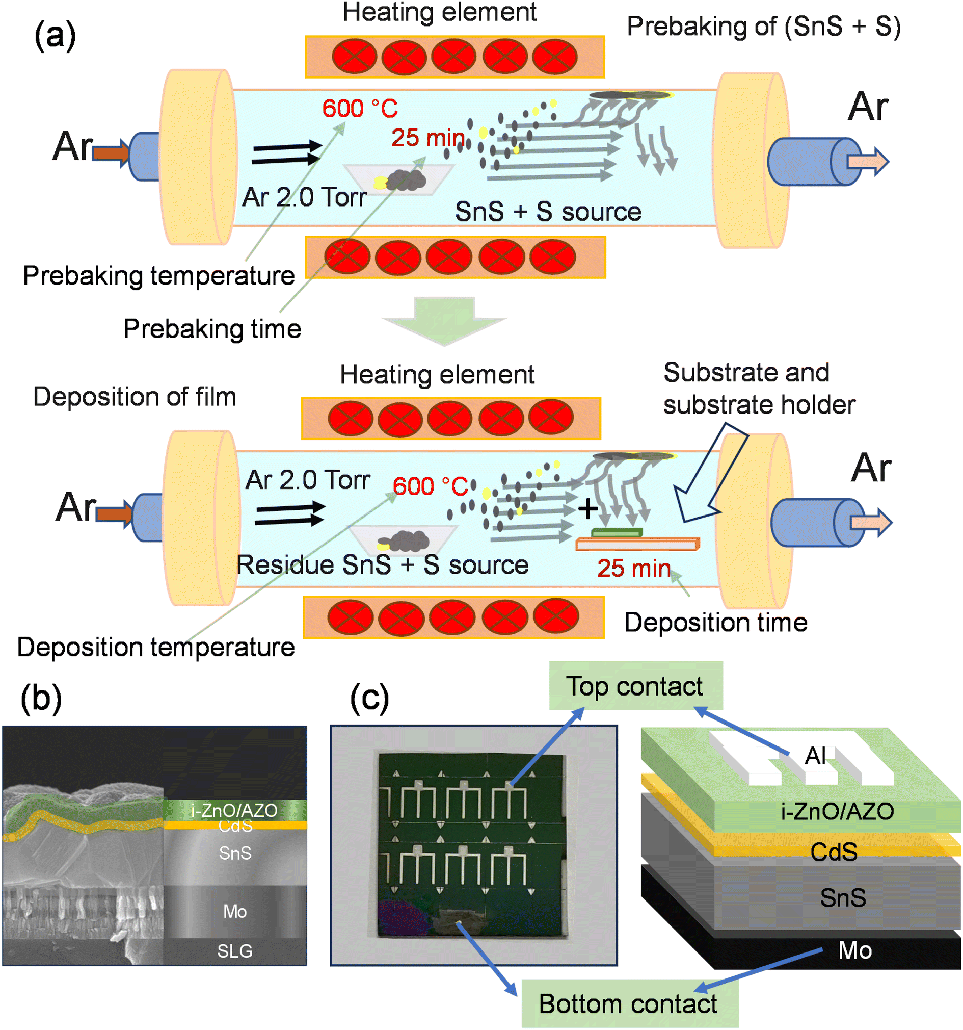 | ||
| Fig. 1 (a) Schematic of the vapor transport deposition (VTD) furnace during prebaking and thin film deposition, (b) schematic and real cross-section scanning emission microscopy (SEM) image of the device showing different layers, and (c) picture of the fabricated device with the schematic. | ||
In this study, first, we optimized the prebaking temperature of the SnS source mixed with a very small amount of S flakes at a fixed prebaking time of 20 min, and the morphological features of the prebaked source SnS thin film at different prebaking temperatures were analyzed using FE-SEM (Fig. S1a & b† of the ESI†). Most of the samples exhibited an almost cube-like morphology with different crystal sizes. The crystal size of the film increased with an increase in the prebaking temperature (Fig S1a of the ESI†); however, the film thickness reduced slightly with an increase in the prebaking temperature (Fig. S1b of the ESI†). The surfaces of the samples prebaked at 600 and 650 °C were comparatively flat. The film thickness was approximately ∼1.3 ± 0.3 μm, accounting for the roughness of the films. The crystal formation of the prebaked SnS source films at different prebaking temperatures was analyzed using XRD. The XRD patterns of all the films were obtained in the 2θ range of 10 to 90°, and for a clearer visualization, the pattern was magnified in the 2θ range of 20 to 40° (Fig. S1c of the ESI†). All the films exhibited a polycrystalline nature, and all the peak positions were well matched with the JCPDS card (01-075-1803), confirming the formation of orthorhombic SnS.
To understand the effect of the prebaking temperature on the morphology and crystal structure of the thin film, the texture coefficient (TC) of different planes was calculated (Fig. S1d†). The (131), (021), (111), (110), (101), and (120) planes varied significantly after prebaking the SnS source. Additionally, the growth along the (131) and (021) planes increased, resulting in the compact and uniform growth of the film deposited using the prebaked source at 600 °C. When the SnS source was prebaked with a small amount of S flakes, favorable crystal growth in the vertical and horizontal directions was observed in the cross-sectional SEM image (Fig. S1b†). The XRD patterns of SnS and S source powder are shown in Fig. S1e† to establish a comparison between the deposited film and source powders.
To investigate the effects of the prebaking temperature on the PV output results, a prebaked SnS source with a small amount of sulfur was deployed as an absorber and CdS as the buffer layer to fabricate TFSCs. The PV parameters as a function of the prebaking temperature are shown in Fig. S2 of the ESI.† With an increase in the prebaking temperature, all the PV parameters increased and reached a peak at 600 °C, after which they started to decline. The VOC of the device slightly increased with increase in temperature, and as the temperature increased beyond 600 °C, VOC shows a slight decline from its peak. This could be attributed to the increase in the film surface quality after prebaking which enhances the interface quality.21 The JSC of the device increased with prebaking temperature, and this could be due to reduction in grain boundary with increase in grain size. The performance of the devices with a change in the prebaking temperature is presented in Table S1† of the ESI. The device fabricated using the “SnS + S” source prebaked at 600 °C exhibited the highest performance (4.72%), with a VOC of 0.346 V, JSC of 25.77 mA cm−2 and fill factor (FF) of 53%. Additionally, the six cells in the device fabricated using the “SnS + S” source prebaked at 600 °C exhibited enhanced performance uniformity compared to other devices. Consequently, the “SnS + S” source prebaked at 600 °C was used for additional studies.
Next, we optimized the prebaking time of the “SnS + S” source at a prebaking temperature of 600 °C to get optimized PV performance. The prebaking time of the “SnS + S” source was varied from 15 to 45 min. The top surface and cross-sectional morphology of the films at different prebaking times are shown in Fig. S3a and b of the ESI.† With an increase in the prebaking time, the crystal size of the films increased (Fig. S3a†), resulting in an increase in the surface roughness. Additionally, with an increase in the prebaking time, the thickness of the films increased slightly (Fig. S3b of the ESI†). The increase in film thickness with increase in prebaking time could be owing to an increase in the deposited amount of evaporated “SnS + S” on the wall of the tube during prebaking, leading to an increase in the film thickness by way of the redeposition of the material deposited on the wall during film deposition. To obtain more information on the surface profile, the AFM measurement was conducted in non-contact mode (Fig. S3c of the ESI†). The surface roughness of the film increased as the prebaking time increased beyond 25 min, owing to unusual increase in grain growth in certain directions. To confirm the surface roughness, AFM measurement (3D) of the films as a function of prebaking time was carried out as shown in Fig. S4a–d of the ESI† and the results are consistent with SEM. The PV parameters of the devices as a function of the prebaking time were investigated under 1-sun illumination, and the results are shown in Fig. S5.† The average values of the PV parameters (VOC, JSC, FF, and η) are presented in Fig. S5a–d.† The best performing device parameters as a function of the prebaking time are tabulated in Table 1.
| Substrate | VTD-SnS | Prebaking time (min) | Cell performance | |||||
|---|---|---|---|---|---|---|---|---|
| Pressure | Temp. (°C) | Deposition time (min) | J SC (mA cm−2) | V OC (V) | FF (%) | η (%) | ||
| SLG/Mo | 2.0 Torr | 600 | 25 | 15 | 21.41 | 0.320 | 54 | 3.7 |
| SLG/Mo | 2.0 Torr | 600 | 25 | 25 | 25.87 | 0.339 | 55 | 4.82 |
| SLG/Mo | 2.0 Torr | 600 | 25 | 35 | 24.8 | 0.333 | 54 | 4.45 |
| SLG/Mo | 2.0 Torr | 600 | 25 | 45 | 26.1 | 0.311 | 53 | 4.30 |
| SLG/Mo | 2.0 Torr | 600 | 25 | Ref. (W.B.) | 21.01 | 0.312 | 51 | 3.39 |
With an increase in the prebaking time, the VOC of the cells remains almost similar, and each cell exhibited improved uniformity. The JSC of the device increased with increase in prebaking time. With an increase in the prebaking time, the thickness of the films remained almost unchanged (a negligible increment), indicating that the thickness of the film was not responsible for increasing JSC. The enhancement in the JSC may be attributed to the decrease in the number of grains and grain boundaries with an increase in the crystal size as the prebaking time increased. The FF of the devices decreased slightly with an increase in the prebaking time. The light J–V curves of all the devices are shown in Fig. S5e.† The device fabricated using the “SnS + S” source film prebaked at 600 °C for 25 min exhibited a champion performance of 4.82% with a VOC, JSC, and FF of 0.339 V, 25.87 mA cm−2, and 55%, respectively.
In the final step, we compared the performance of the optimized prebaked “SnS + S” source film device with the reference device and investigated the parameters affected by prebaking the SnS source with sulfur. To investigate the surface and cross-sectional morphology of the two films, SEM analysis was conducted. The top surface morphologies of the optimized prebaked “SnS + S” source film and W.B. SnS source films are presented in Fig. 2a, and the cross-sectional SEM images of the W.B. SnS source film and “SnS + S” source film prebaked at 600 °C for 25 min are shown in Fig. 2b. The comparison of the W.B. source film with the prebaked source films revealed that the prebaked films exhibited a smoother surface. The thickness of the prebaked SnS source film slightly decreases as compared to the W.B. SnS thin film. This could be attributed to the reduction in the amount of material in the boat after the prebaking process (0.29 g) compared to that of the W.B. source (0.32 g), resulting in a decrease in the film thickness. With an increase in the prebaking time, the film thickness decreased from 1.5 ± 0.2 (W.B. SnS source film) to 1.3 ± 0.2 μm (prebaked “SnS + S” source at 600 °C for 25 min). The crystallinity and phase purity of the optimized prebaked “SnS + S” source film and W.B. prebaked SnS source film was analyzed using XRD. The XRD patterns of both the films were collected in the 2θ range of 10 to 90° (Fig. 2c), and the pattern was magnified in the 2θ range of 20 to 40° (Fig. 2d). Both the films were polycrystalline in nature, and the peak positions of both the films were well matched with the JCPDS card (01-075-1803), confirming the formation of orthorhombic SnS under both conditions. The intensity of the (131) and (021) peaks of the prebaked “SnS + S” source film slightly increased compared to that of the W.B. SnS source film. To understand the effect of prebaking on the morphology and crystal structure of the prebaked “SnS + S” source film compared to W.B. SnS source film, the TC of different planes was calculated (Fig. 2e). The (131), (021), (111), (110), (101), and (120) planes varied significantly after prebaking the SnS source. Additionally, the growth along the (131) and (021) planes increased, resulting in the compact and uniform growth of the film deposited using the prebaked “Sn + S” source. The phase purity of the films was analyzed using Raman spectroscopy at different laser powers (Fig. S6a & b†). The Raman peaks were observed at 51, 94, 170, and 223 cm−1 for the W.B. SnS thin film, and the dominating peaks were 94 and 223 cm−1.22–24 The prebaked “SnS + S” exhibits a similar feature with a slight shift in 94 peak to 96 cm−1, and 170 peak to 168 cm−1. The Raman spectra of orthorhombic SnS thin films show 12 active modes of Raman peaks (4 Ag peaks, 2 B1g peaks, 4 B2g peaks, and 2 B3g peaks) and 7 infrared active modes of Raman peaks (3 B1u, 1 B2u, 3 B3u). In the present study, Raman spectra of both the SnS thin-films deposited using VTD show two intense Raman peaks at 94 ± 2 and 223 ± 2 cm−1 and these peaks belong to Ag active mode of Raman spectra. Moreover, the broad spectral peak that appeared in the wavenumber range 170 ± 4 cm−1 belongs to B2u Raman modes of SnS. Furthermore, a small peak at 285 cm−1 is identified as B3g. Additionally, no notable secondary phases were detected in the Raman spectra of the prebaked “SnS + S” source film and W.B. SnS source films at a lower power of the laser source, except a SnS2 peak at 313 cm−1 at a higher power of the laser source, indicating their phase purity. At the higher power of the laser source, the crystallinity of the film may be affected by the laser source. The Raman analysis was deployed to estimate quantitative assessment of the [Sn]![[thin space (1/6-em)]](https://www.rsc.org/images/entities/char_2009.gif) :[S] ratio. By utilizing the relative shift between different modes of Raman analysis the [Sn]:[S] ratio was evaluated.23 The [Sn]:[S] ratio decreases from 1.5 (W.B. SnS source film) to 1.3 (prebaked SnS + S source film at 600 °C for 25 min) after prebaking of the SnS source with sulfur. Furthermore, EDAX analysis was performed to compare the elemental mapping and atomic ratio of the two films. The sulfur content in the prebaked SnS source film was increased after the prebaking of the (SnS + S) source as compared to the W.B. SnS source film by ∼5% (Fig. S7†), and this may be attributed to the re-deposition of the pre-evaporated material, which was deposited on the wall of the tube during the prebaking of the SnS source with a small amount of sulfur powder (0.015 g). The experimental error limit is about 2%, consequently the difference in atomic percentage of the constituent is outside the error limit. The VTD-SnS shows deficiency of S in the form of S vacancy (VS) and an increase in the sulfur content in the film to a certain extent is beneficial for the VTD-SnS device performance, as it reduces the VS.25–27 Here, EDAX of the thin film deposited on a Mo substrate was performed. Mo and S peaks coincide with each other in EDAX analysis measurement. This could be the reason behind the observation of the atomic ratios of “Sn” being lower than those of “S” in the EDAX measurement. Also, EDAX analysis is not a sufficient technique to confirm the exact composition, and stoichiometry. In this manuscript, EDAX analysis was used to compare the composition of the two films. EDAX and Raman both analyses result in a similar observation of increase in sulfur content after prebaking of the “SnS + S” source.
:[S] ratio. By utilizing the relative shift between different modes of Raman analysis the [Sn]:[S] ratio was evaluated.23 The [Sn]:[S] ratio decreases from 1.5 (W.B. SnS source film) to 1.3 (prebaked SnS + S source film at 600 °C for 25 min) after prebaking of the SnS source with sulfur. Furthermore, EDAX analysis was performed to compare the elemental mapping and atomic ratio of the two films. The sulfur content in the prebaked SnS source film was increased after the prebaking of the (SnS + S) source as compared to the W.B. SnS source film by ∼5% (Fig. S7†), and this may be attributed to the re-deposition of the pre-evaporated material, which was deposited on the wall of the tube during the prebaking of the SnS source with a small amount of sulfur powder (0.015 g). The experimental error limit is about 2%, consequently the difference in atomic percentage of the constituent is outside the error limit. The VTD-SnS shows deficiency of S in the form of S vacancy (VS) and an increase in the sulfur content in the film to a certain extent is beneficial for the VTD-SnS device performance, as it reduces the VS.25–27 Here, EDAX of the thin film deposited on a Mo substrate was performed. Mo and S peaks coincide with each other in EDAX analysis measurement. This could be the reason behind the observation of the atomic ratios of “Sn” being lower than those of “S” in the EDAX measurement. Also, EDAX analysis is not a sufficient technique to confirm the exact composition, and stoichiometry. In this manuscript, EDAX analysis was used to compare the composition of the two films. EDAX and Raman both analyses result in a similar observation of increase in sulfur content after prebaking of the “SnS + S” source.
EDAX (presented in Fig. S7†) alone was not sufficient to confirm the atomic percent of the elements and stoichiometry in the film, consequently we performed XPS analysis of the two absorbers to confirm the chemical composition and evaluate the atomic fraction of Sn and S in both absorbers (Fig. S8a & b†). The calculated atomic fraction of “S” in the prebaked SnS source film increased by ∼4% compared to the reference (W.B. SnS source) film, which is almost consistent with EDAX analysis and confirms the increase of “S” content in the prebaked “SnS + S” source film. The [Sn]:[S] ratio estimated from Raman analysis was found in approximation of the ratio calculated using XPS analysis.
To investigate the effect of prebaking of the “SnS + S” source on device performance, we compared the PV output of the devices of the two absorbers. The devices fabricated using the prebaked “SnS + S” source exhibited improvement in all the PV parameters. Fig. 3a–d show the comparison of the PV parameters of the champion cells of the prebaked (SnS + S source film prebaked at 600 °C for 25 min) and reference (W.B. SnS source film) devices. The light J–V curve, the dark J–V curve, bandgap extracted from EQE, and EQE spectrum of the champion prebaked “SnS + S” source and reference devices are presented in Fig. 3e–h respectively.
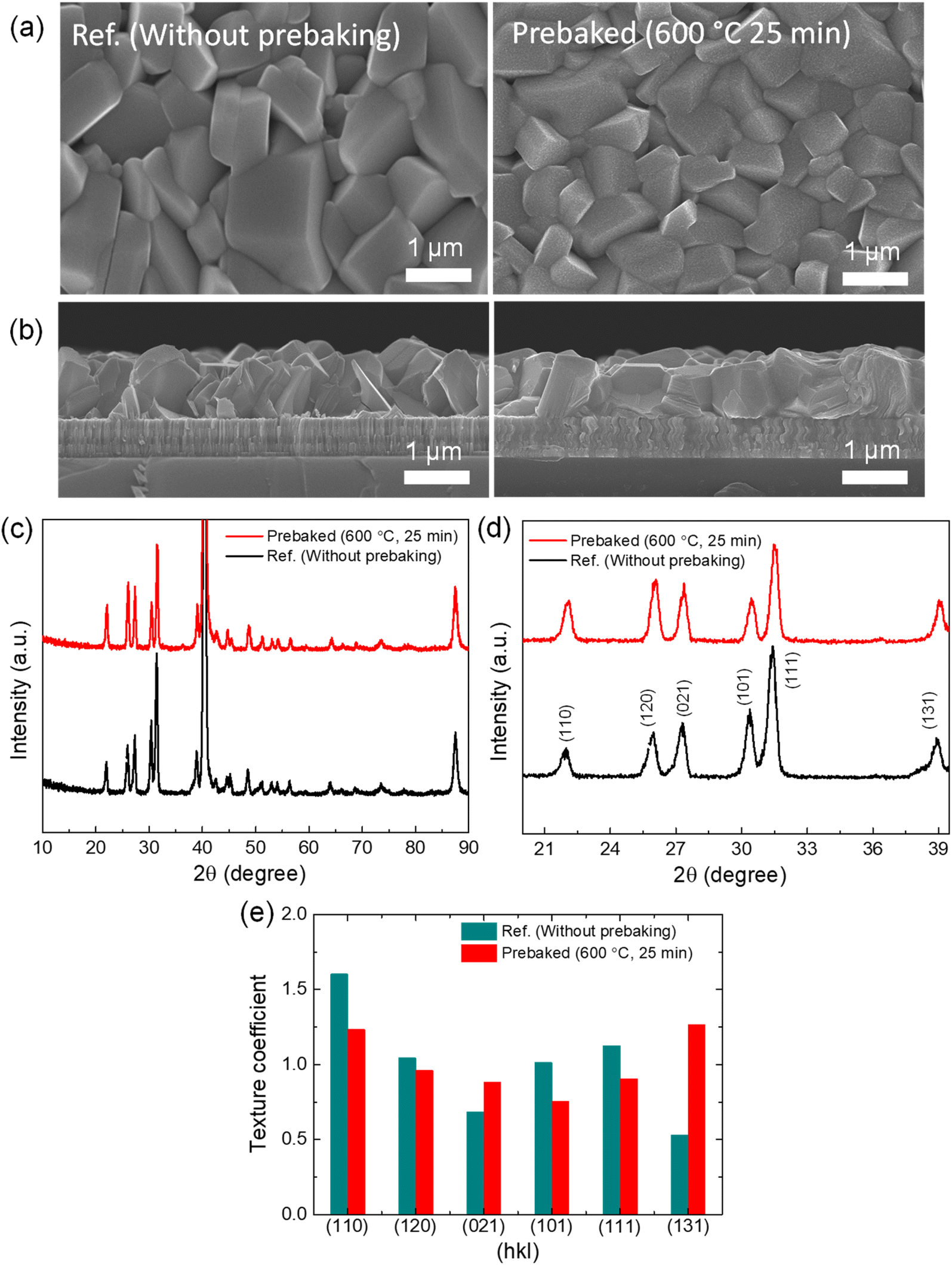 | ||
| Fig. 2 SEM image of the without prebaking (W.B.; ref.) and 600 °C-prebaked SnS: (a) top surface morphology, (b) cross-section, (c) X-ray diffraction (XRD) pattern of the W.B. and prebaked source films in the 2θ range of 10 to 90°, (d) XRD pattern of the W.B. and prebaked source films in the 2θ range of 20 to 40°, and (e) the calculated texture coefficient of different planes. | ||
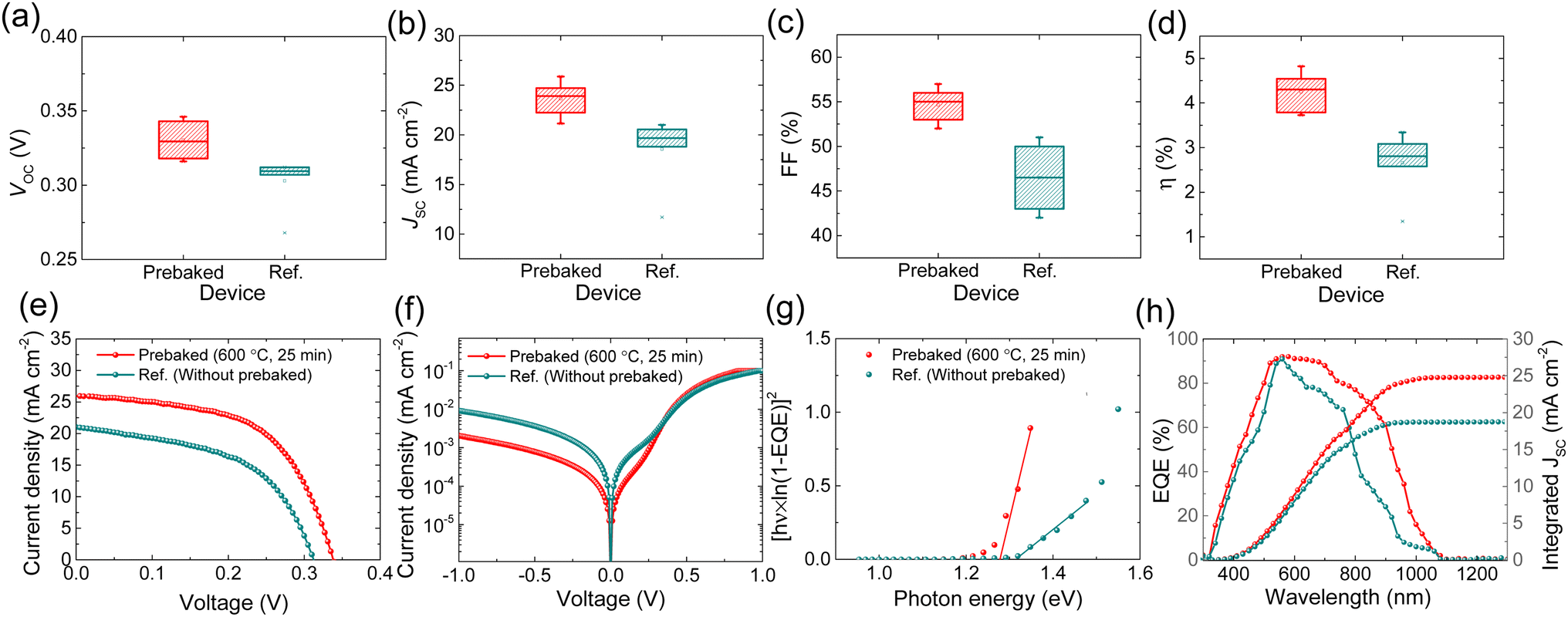 | ||
| Fig. 3 Box plot of the PV parameters of the devices fabricated using the ref. (W.B.) SnS and prebaked “SnS + S” source films: (a) open circuit voltage (VOC), (b) short circuit density (JSC), (c) fill factor (FF), and (d) η, and (e) light J–V curve, (f) dark J–V curve, (g) bandgap extracted from the EQE profile, and (h) EQE response and integrated JSC from EQE. | ||
The devices fabricated using the prebaked “SnS + S” source exhibited improved VOC compared to the device fabricated using the W.B. SnS source film. This improvement in VOC could be attributed to the reduction in VOC deficit. The SnS thin-film solar cells reflect a large VOC deficit, which limits the performance of SnS based TFSCs. Band tailing effects, which usually arise from deep defects at the heterojunction interface (due to a large amount of VS) and within the space charge region, are known to be one of the primary reasons for the device performance deterioration, especially the large VOC deficit. It can be clearly seen that the VOC deficit of the champion device (prebaked SnS + S source) in this work is much lower than that of the reference (W.B. SnS source) solar cell, confirming the effectiveness of the prebaking strategy in reducing VOC deficit. The JSC of the prebaked SnS source devices increased from 21.01 to 25.87 mA cm−2, resulting in an increase in the device performance. The EQE responses of the two devices fabricated using the prebaked “SnS + S” source and W.B. SnS source were recorded. The EQE response of the prebaked “SnS + S” source device showed improvement in the entire wavelength region compared to that of the device fabricated using the W.B. SnS source, which led to improvement in JSC. The prebaking of the SnS source with sulfur reduced the sulfur vacancies as clearly seen from XPS analysis, and we believe this resulted in the suppression of bulk defect and trap centers, which enhanced the charge collection.28 The FF of the prebaked SnS device shows a similar trend in enhancement to that of VOC and JSC.
We extracted the bandgap of the two films from the EQE response of the two devices. The bandgap of the prebaked “SnS + S” source films slightly decreased, which could be attributed to the decrease in the crystal size of the prebaked film along with an increase in the sulfur content in the film. Furthermore, the change in bandgap, to a very small extent, could be attributed to reduction in the deviation of the stoichiometric ratio of Sn to S up to an extent with increase in S content.29–32 The EQE and integrated JSC of both the devices are shown in Fig. 3h. The integrated JSC extracted from the EQE is consistent with the JSC observed from the light J–V characteristic curve and tabulated in Table 2. To investigate the relationship between the diode properties and PV output parameters of both the champion devices, the dark J–V measurement was conducted in the bias range of −1 to 1 V, and the results are presented in Fig. 3f. The heterojunction diode parameters, that is, the shunt conductance (GS), series resistance (RS), ideality factor (A), and dark saturation current density (J0) were extracted from the dark J–V measurement and are shown in Fig. 4. The variation in the diode parameters as a function of the prebaking time and reference are presented in Table S2 of the ESI.†
| Prebaking time (min) | Integrated JSC (mA cm−2) | J SC from light J–V (mA cm−2) |
|---|---|---|
| 15 | 20.38 | 21.41 |
| 25 | 25.39 | 25.87 |
| 35 | 24.83 | 24.8 |
| 45 | 25.39 | 26.1 |
| Ref. (W.B.) | 19.24 | 21.01 |
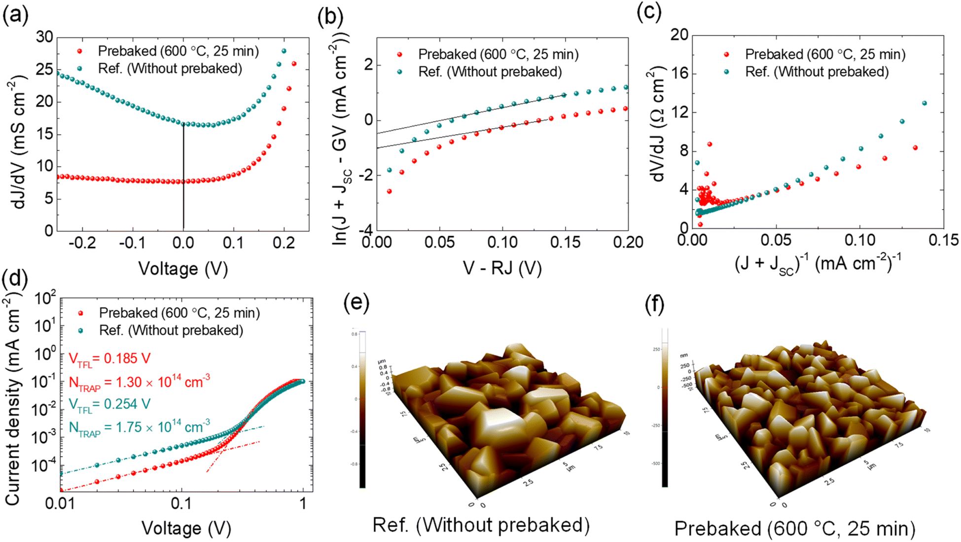 | ||
| Fig. 4 Dark J–V behavior of the prebaked and W.B. film-based devices. (a) Shunt conductance, (b) reverse saturation current, (c) series resistance with ideality factor, (d) full logarithmic characteristics of the J–V curve, and (e and f) AFM topography of the ref. and prebaked source films. | ||
The GS of the device fabricated using the prebaked “SnS + S” source film was lower than that of the device fabricated using the W.B. SnS source film, indicating that the prebaking of the “SnS + S” source improved the shunt properties (Fig. 4a). The J0 of the device fabricated using the prebaked “SnS + S” source film reduced, indicating the improved transportation of the generated charge carriers (Fig. 4b).33,34 Improvement in A of the prebaked “SnS + S” source device (1.4) compared to the W.B. SnS device (3.6) indicates the improvement in heterojunction interface with prebaking of the SnS source with sulfur (Fig. 4c). The opposite trend for RS was observed with prebaking of the “SnS + S” source and it increased from 0.52 to 1.65 Ω cm2.
Defects in bulk behave like recombination centers and worsen the performance of devices. The full logarithmic characteristics of the dark J–V curve were used to calculate the trap field limit voltage (VTFL) of the best cells of both the devices.35 The VTFL of the prebaked champion device was 0.185 V, and that of the device fabricated using the W.B. SnS source film was 0.254 V (Fig. 4d). The trap densities (defect density, Ntrap) of the reference and champion devices were calculated using the following equation:36
 | (1) |
Furthermore, the behavior of the interface defect and carrier concentration in the prebaked “SnS + S” source film and W.B. SnS source films were investigated using C–V measurement (Fig. 5). The built-in potential (Vbi) of the fabricated champion cells was evaluated by extrapolating 1/C2versus V plot by linear fitting towards the voltage axis (Fig. 5a–b). The evaluated Vbi of the device fabricated using the prebaked “SnS + S” source absorber was smaller than that of the device fabricated using the W.B. SnS source film. The carrier concentration in the prebaked “SnS + S” source absorber (4.30 × 1016 cm−3) was considerably smaller than that in the W.B. SnS source absorber (2.16 × 1017 cm−3; Fig. 5c). The depletion width of the prebaked “SnS + S” source-based device was 209 nm, whereas that of the device fabricated using the W.B. SnS source was 110 nm. The higher carrier concentration suppressed the depletion width of the device fabricated using the W.B. SnS source film, resulting in a loss in the carrier collection. In contrast, owing to its lower carrier concentration and broader depletion width, the collection of the generated charge carrier in the device fabricated using the prebaked “SnS + S” source was enhanced. The lower carrier concentration in the device fabricated using the prebaked “SnS + S” sources could be attributed to the reduction in sulfur vacancies, which resulted in a decrease in the trap density.
Next, to confirm the oxidation state of Sn in the films we have fitted the Sn 3d and S 2p core level peaks of XPS measurement (Fig. 6a–d). The Sn 3d5/2 and Sn 3d3/2 peaks were centered at 484.8 and 494.1 eV, respectively, which indicates an Sn2+ valence state (Fig. 6a and c). Furthermore, the peaks at slightly higher binding energies of 485.6 and 495.1 eV were associated with the Sn4+ state, which might originate from the SnO2 layer formed due to the surface oxidation of SnS. The S 2p peaks were centered at 160.5 and 161.8 eV, corresponding to S 2p3/2 and S 2p1/2, respectively, indicative of the divalent nature of the S ion (Fig. 6b and d).39,40 To confirm the surface oxidation and formation of SnO2, we fitted the oxygen peak observed in the surface XPS analysis of the two films and, the possibility of the SnO2 phase was observed (Fig. S9 of the ESI†).
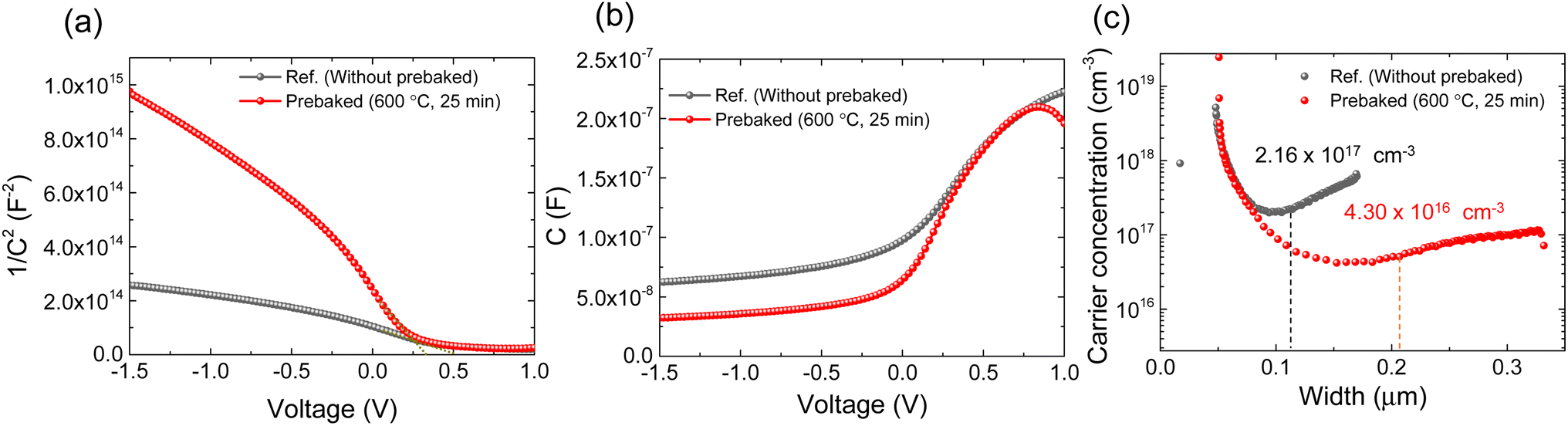 | ||
| Fig. 5 (a) 1/C2versus V curve, (b) C–V curve, (c) carrier concentration versus depletion width of the best cells of ref. (W.B. SnS source) and prebaked SnS source film devices. | ||
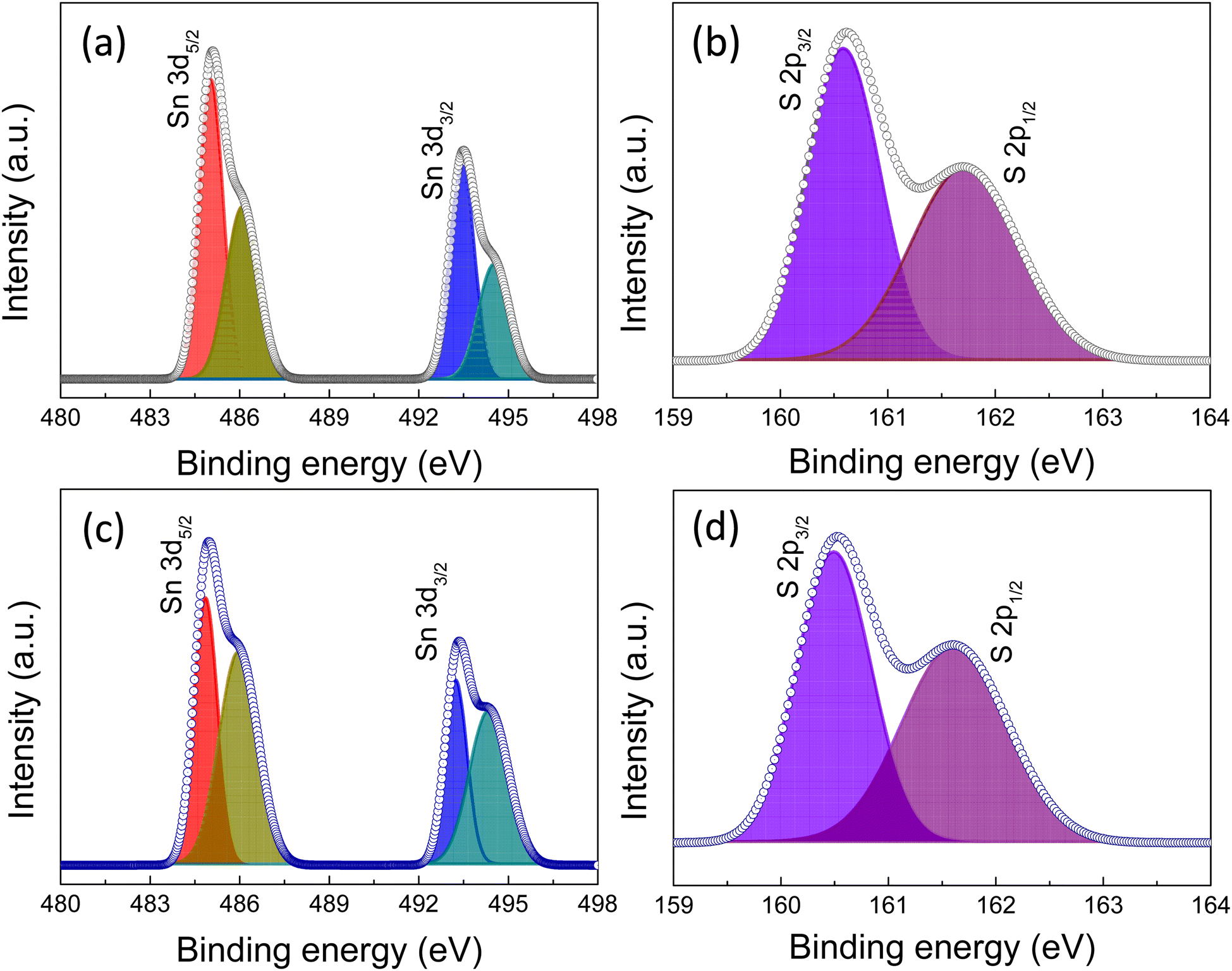 | ||
| Fig. 6 (a) XPS spectra of Sn 3d, (b) S 2p peaks of without prebaked SnS source films, (c) Sn 3d, and (d) S 2p peaks of the prebaked SnS source film. | ||
In this paper, we reported the highest PCE for SnS-based TFSCs and opened a path towards fabricating SnS-based TFSCs with an efficiency above 5%. A comparison of top performing devices (efficiency above 4%) deposited by different techniques is provided in Table 3. Additionally, we examined the stability of the fabricated best device after six months of air exposure, and the results are shown in Fig. S10 of the ESI.† The results revealed that the device retained 88% of its initial efficiency.
| Device structure | Deposition method | V OC (V) | J SC (mA cm −2) | FF (%) | η (%) | Year |
|---|---|---|---|---|---|---|
| SLG/Mo/SnS/SnO2/Zn(O,S):N/ZnO/ITO | ALD | 0.372 | 20.2 | 58 | 4.36 | 2014 (ref. 16) |
| Au/SnS/ns-TiO2/FTO | Solution processed | 0.330 | 24.7 | 58 | 4.8 | 2019 (ref. 15) |
| SLG/Mo/SnS/CdS/i-ZnO/AZO/Al | VTD | 0.346 | 20.76 | 58 | 4.22 | 2020 (ref. 19) |
| SLG/Mo/SnS/CdS/i-ZnO/AZO/Al | VTD | 0.339 | 25.87 | 55 | 4.82 | This work |
4. Conclusion
In this study, we analyzed the significant improvement in the performance of a VTD-SnS solar cell fabricated using an absorber source prebaked with a small amount of sulfur before the absorber layer deposition. The sulfur content in the film increased by 5%, which resulted in the suppression of the VS in the film, thus reducing the deep level defect. The suppression in the defect led to improvements in the VOC and JSC of the device, thus the overall performance of the device increased from 3.39% (for the device fabricated using the W.B. source film) to 4.82% (for the device fabricated using the prebaked source film). Additionally, we observed that the surface roughness of the film reduced slightly after prebaking compared to the W.B. film; consequently, a better heterojunction could be fabricated using the prebaked source film, which is evident from the improved diode properties. The FF of the device fabricated using the prebaked source film was enhanced compared to that of the device fabricated using the W.B. film. We believe that this work will be helpful in providing an easy and implicit process to improve the performance of SnS-based TFSCs beyond 5% efficiency.Author contributions
R. K. Yadav: conceptualization, methodology, investigation, experimental, data curation, and writing (original and final draft). P. S. Pawar: formal analysis and data curation. I. Sharma: formal analysis and resources. Y. T. Kim: formal analysis and resources. J. Heo: resources, funding acquisition, validation, supervision and writing (original and final draft). All authors have approved the final version of the manuscript.Conflicts of interest
The authors declare no competing financial interest.Acknowledgements
This study was supported by the National Research Foundation of Korea (NRF) grant funded by the Korean government (2022R1A2C2006532, 2018R1A6A1A03024334).References
- K. Yoshikawa, H. Kawasaki, W. Yoshida, T. Irie, K. Konishi, K. Nakano, T. Uto, D. Adachi, M. Kanematsu, H. Uzu and K. Yamamoto, Nat. Energy, 2017, 2, 1–8 CrossRef.
- U. Paetzold, M. Jaysankar, R. Gehlhaar, E. Ahlswede, S. Paetel, W. Qiu, J. Bastos, L. Rakocevic, B. Richards, T. Aernouts, M. Powalla and J. Poortmans, J. Mater. Chem. A, 2017, 5, 9897–9906 RSC.
- J. Ramanujam, D. M. Bishop, T. K. Todorov, O. Gunawan, J. Rath, R. Nekovei, E. Artegiani and A. Romeo, Prog. Mater. Sci., 2020, 110, 100619 CrossRef CAS.
- A. Wang, M. He, M. A. Green, K. Sun and X. Hao, Adv. Energy Mater., 2023, 13, 2203046 CrossRef CAS.
- L. Huang, S. Wei and D. Pan, ACS Appl. Mater. Interfaces, 2018, 10, 35069–35078 CrossRef CAS PubMed.
- G. H. Albuquerque, K.-J. Kim, J. I. Lopez, A. Devaraj, S. Manandhar, Y.-S. Liu, J. Guo, C.-H. Chang and G. S. Herman, J. Mater. Chem. A, 2018, 6, 8682–8692 RSC.
- R. Tang, S. Chen, Z. H. Zheng, Z. H. Su, J. T. Luo, P. Fan, X. H. Zhang, J. Tang and G. X. Liang, Adv. Mater., 2022, 34, 2109078 CrossRef CAS PubMed.
- J. Zhou, X. Xu, H. Wu, J. Wang, L. Lou, K. Yin, Y. Gong, J. Shi, Y. Luo, D. Li, H. Xin and Q. Meng, Nat. Energy, 2023, 8, 526–535 CrossRef CAS.
- X. Lv, W. Wei, C. Mu, B. Huang and Y. Dai, J. Mater. Chem. A, 2018, 6, 5032–5039 RSC.
- M. Patel and A. Ray, ACS Appl. Mater. Interfaces, 2014, 6, 10099–10106 CrossRef CAS PubMed.
- P. Sinsermsuksakul, J. Heo, W. Noh, A. S. Hock and R. G. Gordon, Adv. Energy Mater., 2011, 1, 1116–1125 CrossRef CAS.
- D. Lim, H. Suh, M. Suryawanshi, G. Y. Song, J. Y. Cho, J. H. Kim, J. H. Jang, C. W. Jeon, A. Cho, S. Ahn and J. Heo, Adv. Energy Mater., 2018, 8, 1702605 CrossRef.
- S. Hadke, M. Huang, C. Chen, Y. F. Tay, S. Chen, J. Tang and L. Wong, Chem. Rev., 2021, 122, 10170–10265 CrossRef PubMed.
- V. Steinmann, R. Jaramillo, K. Hartman, R. Chakraborty, R. E. Brandt, J. R. Poindexter, Y. S. Lee, L. Sun, A. Polizzotti, H. -H. Park, R. G. Gordon and T. Buonassisi, Adv. Mater., 2014, 26, 7488–7492 CrossRef CAS PubMed.
- H. S. Yun, B. w. Park, Y. C. Choi, J. Im, T. J. Shin and S. I. Seok, Adv. Energy Mater., 2019, 9, 1901343 CrossRef.
- P. Sinsermsuksakul, L. Sun, S. Lee, H. Park, S. Kim, C. Yang and R. G. Gorden, Adv. Energy Mater., 2014, 4, 1400496 CrossRef.
- N. Spalatu, J. Hiie, R. Kaupmees, O. Volobujeva, J. Krustok, I. Oja Acik and M. Krunks, ACS Appl. Mater. Interfaces, 2019, 11, 17539–17554 CrossRef CAS PubMed.
- H. Fu, J. Mater. Chem. C, 2018, 6, 414–445 RSC.
- J. Y. Cho, S. Kim, R. Nandi, J. Jang, H.-S. Yun, E. Enkhbayar, J. H. Kim, D.-K. Lee, C.-H. Chung, J. Kim and J. Heo, J. Mater. Chem. A, 2020, 8, 20658–20665 RSC.
- R. K. Yadav, P. S. Pawar, K. E. Neerugatti, R. Nandi, J. Y. Cho and J. Heo, Curr. Appl. Phys., 2021, 31, 232–238 CrossRef.
- C. Wu, L. Zhang, B. Che, P. Xiao, J. Yang, H. Wang, L. Chu, W. Yan and T. Chen, J. Mater. Chem. A, 2023, 11, 8184–8191 RSC.
- I. Y. Ahmet, M. Guc, Y. Sánchez, M. Neuschitzer, V. Izquierdo-Roca, E. Saucedo and A. L. Johnson, RSC Adv., 2019, 9, 14899–14909 RSC.
- M. Guc, J. Andrade-Arvizu, I. Y. Ahmet, F. Oliva, M. Placidi, X. Alcobé, E. Saucedo, A. Pérez-Rodríguez, A. L. Johnson and V. Izquierdo-Roca, Acta Mater., 2020, 183, 1–10 CrossRef CAS.
- V. K. Arepalli, Y. Shin and J. Kim, Superlattices Microstruct., 2018, 122, 253–261 CrossRef CAS.
- W. Wang, Z. Cao, H. Wang, J. Luo and Y. Zhang, J. Mater. Chem. A, 2021, 9, 26963–26975 RSC.
- V. R. Minnam, H. Cho, S. Gedi, K. R. Reddy, W. K. Kim and C. Park, J. Alloys Compd., 2019, 806, 410–417 CrossRef.
- S. Di Mare, D. Menossi, A. Salavei, E. Artegiani, F. Piccinelli, A. Kumar, G. Mariotto and A. Romeo, Coatings, 2017, 7, 34 CrossRef.
- K. Rudisch, A. Davydova, L. Riekehr, J. Adolfsson, L. Q. Casal, C. Platzer-Björkman and J. Scragg, J. Mater. Chem. A, 2020, 8, 15864–15874 RSC.
- P. Nwofe, R. Miles and K. Ramakrishna Reddy, J. Renewable Sustainable Energy, 2013, 5, 011204 CrossRef.
- M. Gurubhaskar, N. Thota, M. Raghavender, G. H. Chandra, P. Prathap and Y. V. Subbaiah, Vacuum, 2018, 155, 318–324 CrossRef CAS.
- R. Dahule, C. C. Singh, K. Hongo, R. Maezono and E. Panda, J. Mater. Chem. C, 2022, 10, 5514–5525 RSC.
- T. S. Reddy and M. S. Kumar, RSC Adv., 2016, 6, 95680–95692 RSC.
- S. Hegde, P. Murahari, B. J. Fernandes, R. Venkatesh and K. Ramesh, J. Alloys Compd., 2020, 820, 153116 CrossRef CAS.
- W. Wang, Z. Cao, X. Zuo, L. Wu, J. Luo and Y. Zhang, J. Energy Chem., 2022, 70, 191–200 CrossRef CAS.
- K. Chen, P. Wu, W. Yang, R. Su, D. Luo, X. Yang, Y. Tu, R. Zhu and Q. Gong, Nano Energy, 2018, 49, 411–418 CrossRef CAS.
- Y. Luo, G. Chen, S. Chen, N. Ahmad, M. Azam, Z. Zheng, Z. Su, M. Cathelinaud, H. Ma, Z. Chen, P. Fan, X. Zhang and G. Liang, Adv. Funct. Mater., 2023, 33, 2213941 CrossRef CAS.
- H. T. Nguyen, V. L. Le, T. M. H. Nguyen, T. J. Kim, X. A. Nguyen, B. Kim, K. Kim, W. Lee, S. Cho and Y. D. Kim, Sci. Rep., 2020, 10, 18396 CrossRef CAS PubMed.
- P. Akata Nwofe and M. Sugiyama, Phys. Status Solidi A, 2020, 217, 1900881 CrossRef CAS.
- I.-H. Baek, J. J. Pyeon, Y. G. Song, T.-M. Chung, H.-R. Kim, S.-H. Baek, J.-S. Kim, C.-Y. Kang, J.-W. Choi, C. S. Hwang, J. H. Han and S. K. Kim, Chem. Mater., 2017, 29, 8100–8110 CrossRef CAS.
- P. Jain and P. Arun, Thin Solid Films, 2013, 548, 241–246 CrossRef CAS.
Footnote |
| † Electronic supplementary information (ESI) available. See DOI: https://doi.org/10.1039/d3ta05204d |
| This journal is © The Royal Society of Chemistry 2024 |