
 Open Access Article
 This Open Access Article is licensed under a Creative Commons Attribution-Non Commercial 3.0 Unported Licence
Efficiency enhancement and doping type inversion in Cu2CdSnS4 solar cells by Ag substitution†
Ahmad
Ibrahim
 a,
Stener
Lie
ab,
Joel Ming Rui
Tan
ab,
Ryan
Swope
c,
Axel Gon
Medaille
def,
Shreyash
Hadke
c,
Edgardo
Saucedo
ef,
Rakesh
Agrawal
c and
Lydia Helena
Wong
*abg
a,
Stener
Lie
ab,
Joel Ming Rui
Tan
ab,
Ryan
Swope
c,
Axel Gon
Medaille
def,
Shreyash
Hadke
c,
Edgardo
Saucedo
ef,
Rakesh
Agrawal
c and
Lydia Helena
Wong
*abg
aSchool of Materials Science and Engineering, Nanyang Technological University, Singapore 639798, Singapore. E-mail: lydiawong@ntu.edu.sg
bCampus for Research Excellence and Technological Enterprise (CREATE), Singapore 138602, Singapore
cDavidson School of Chemical Engineering, Purdue University, West Lafayette, Indiana 47907, USA
dSolar Energy Materials and Systems Group, Catalonia Institute for Energy Research (IREC), Jardins de les Dones de Negre 1, 08930 Sant Adrià de Besòs, Barcelona, Spain
ePhotovoltaic Lab – Micro and Nano Technologies Group (MNT), Electronic Engineering Department, EEBE, Universitat Politècnica de Catalunya (UPC), Av Eduard Maristany 10-14, Barcelona 08019, Catalonia, Spain
fBarcelona Center for Multiscale Science & Engineering, Universitat Politècnica de Catalunya (UPC), Av Eduard Maristany 10-14, Barcelona 08019, Catalonia, Spain
gEnergy Research Institute @ NTU (ERI@N), Nanyang Technological University, Singapore 637553, Singapore
First published on 22nd December 2023
Abstract
The main limiting factor of kesterite-related solar cells is the low open-circuit voltage (VOC) relative to their bandgap. This drawback has been correlated with the easily formed anti-site defects caused by similar ionic radii and/or chemical valence. Recent success in suppressing Sn-related defects by using Cd to replace Zn in Cu2CdSnS4 was attributed to the higher formation energy of the 2CuCd + SnCd defect complex compared to its counterpart in Cu2ZnSnS4. This has motivated the use of bigger ions to replace Cu in Cu2CdSnS4 to reduce the possibilities of III and III defect formation. In this work, we substitute Cu in Cu2CdSnS4 with larger Ag at various concentrations and investigate the structural, optoelectronic, and photovoltaic properties of (Cu,Ag)2CdSnS4. Higher concentrations of Ag lead to peak splitting in XRD spectra, which is attributed to mixed phases and marks the transition towards Ag2CdSnS4. This is also complemented by Raman scattering analysis, the first time the Raman spectrum of Ag2CdSnS4 is reported. Doping type inversion was observed for pure n-type Ag2CdSnS4 instead of the p-type of Cu2CdSnS4, accompanied by high carrier mobility and sharp absorption onset. Further optoelectronic and photovoltaic characterization reveals that adding 5% Ag concentration improves Cu2CdSnS4 device performance to 7.72%, mainly due to superior film quality and improved interface properties. As a result, better carrier collection contributes to the short-circuit current improvement of the champion device.
Introduction
The motivation to address anti-site defects in Cu2ZnSnS4 has led to investigations on I2–II–IV–VI4 compounds as better solar harvesting materials.1,2 Anti-site defects in Cu2ZnSnS4 occur when one cation replaces another with similar or different oxidation states, resulting in point defects such as CuZn, or defect clusters such as 2CuZn + SnZn. To mitigate the formation of these defects, cations with larger ionic size differences are utilized to substitute one or more cations with similar ionic sizes, such as Cu or Zn.3Cation substitution in Cu2ZnSnS4 is a crucial strategy in further improving its performance. The cation substitution on Cu2ZnSnS4 involving the Ag & Cd reduces the VOC deficit caused by both radiative and nonradiative recombination. Partial Cd-alloying of Cu2ZnSnS4 has positively impacted grain quality,4 band alignment,5 and bandgap fluctuations.6 As indicated by lower bandgap fluctuation, Cd substitution limits the sub-bandgap absorption compared to Cu2ZnSnS4 and elevates the valence band maximum (VBM), improving the band alignment.6,7 Similarly, Ag substitution has a positive effect, as indicated by lower Urbach energy and reduced anti-site defects.8 Furthermore, the co-substitution of Ag and Cd on Cu2ZnSnS4 improved device efficiency to 10.2%.9
Full cation substitution of Cu2ZnSnS4 leading to I2–II–IV–VI4 compounds has also been explored to pursue different structural and electronic properties. The lack of Cu vacancy in Ag2ZnSn(S,Se)4 and Zn-rich condition was found to be favorable for forming n-type instead of p-type material.10 Consequently, a different device configuration needs to be employed.11,12 CXTS compounds (where X = Mg, Mn, Ni, Co, Fe, etc.) have been studied as substitutes for Zn. A library of CXTS compounds was successfully fabricated using spray pyrolysis. While Cu2MnSnS4, Cu2BaSnS4, and Cu2SrSnS4 demonstrated good device performances, forming pure phases for some compounds was difficult.13 Efforts have also been made to alloy a high amount of Ge for CZGSe, leading to a 7.6% efficiency and a further 8.5% after surface treatment and heat treatment on a complete device (including MgF2 anti-reflection coating layer).14,15 Among all these cations, Cu2CdSnS4 has the highest device performance so far.
The favorable material properties of Cu2CdSnS4 make it a promising candidate for further development as one of the emerging thin film solar cells. The Cu2CdSnS4 solar cell has shown remarkable device performance, starting with an efficiency of 7.96%, which recently has been improved to 10.1%, placing it among the highest reported efficiency of emerging kesterite-inspired solar cell devices and close to the 11.0% certified record efficiency for pure sulfide Cu2ZnSnS4.16–19 The suppressed 2CuCd + SnCd defect formation, due to its higher formation energy compared to 2CuZn + SnZn in Cu2ZnSnS4, is attributed to the promising properties of this material. Both defect complexes act as deep electron traps3,20 and contribute to the increase of bandgap fluctuation and nonradiative recombination. Cu-Poor condition, commonly employed in kesterite solar cells, further suppressed the 2CuCd + SnCd defect.16 This non-stoichiometric condition and optimized sulfurization configuration were also crucial for the recent device efficiency improvement.17 While the current achievements for Cu2CdSnS4 solar cells are encouraging, additional strategies such as doping and alloying could be important to understand this compound better.
The cation substitution (and doping) strategies in Cu2CdSnS4 have yet to be thoroughly studied. While the beneficial roles of Ag have been observed in partially Cd-substituted Cu2ZnSnS4 compounds, its impact on the material and photovoltaic properties of Cu2CdSnS4 remains unexplored.9,21 Additionally, the absorption coefficient of Ag2CdSnS4 has been calculated to be suitable for a solar cell.22 The larger Ag+ ionic radii (1.00 Å) compared to Cu+ (0.60 Å) suggest that substituting Cu to Ag could further reduce 2CuCd + SnCd defects. Other theoretical works highlighted that as the difference in ionic radii size of Ag–Cd is not as high as Ag–Zn (Ag+ to Cd2+ is 28% larger, while Ag+ to Zn2+ is 66% larger), Ag2CdSnS4 might not be as disorder-resistant as compared to Ag2ZnSnS4.23,24 This work aims to investigate the effect of Ag substitution for Cu2CdSnS4 by comparing phase distribution, film morphology, and device performance as part of its structural, optoelectronic, and photovoltaic properties. The small addition of Ag in Cu2CdSnS4 improved device performance to 7.72% compared to 6.87% reference, but the improvement is limited by the presence of mixed phases at higher Ag concentrations. This limitation will be explored by studying the transformation from Cu2CdSnS4 to Ag2CdSnS4, correlating the transition with the evolution of the device performance. Finally, the fully-substituted Ag2CdSnS4 induced doping type inversion, high carrier mobility, and exhibits a sharp absorption onset.
Results and discussion
In this study, we monotonically modify the concentration of Ag by depositing the precursor solutions using spin-coating, starting from pure Cu2CdSnS4 (Ag/[Ag + Cu] = 0%) to Ag2CdSnS4 (Ag/[Ag + Cu] = 100%). The selection of 5% and 10% Ag was based on the optimal device efficiency observed in previous Cu2ZnSnS4 devices.25–28 The films for all Ag concentrations were characterized for their structural and optoelectronic properties, while only selected concentrations were made into full devices.Structural properties of (Cu1−xAgx)2CdSnS4
The diffractograms (Fig. 1a) obtained from as-fabricated Cu2CdSnS4 film fit the reported database and showed major peaks at 28° and 47° associated with (112) and (204) of the Cu2CdSnS4 stannite plane (JCPDS No. 29-0537). The magnified XRD spectra in the range of 2θ = 23–30° is shown in Fig. 1b, highlighting the transition from tetragonal Cu2CdSnS4 to orthorhombic Ag2CdSnS4 phase. In the range of 0–20% Ag substitution, there is a subtle shift to a lower diffraction angle at the (112) peak due to the successful incorporation of larger Ag ions.29 The slight 40° diffraction angle is from the Mo substrate and thus is used as a reference for the peak shifting for other Ag concentrations. It is observed that the transition from Cu2CdSnS4 towards mixed phases with Ag2CdSnS4 starts at 30% Ag substitution. Starting at this concentration up to 80% Ag, it can also be observed that the film quality is deteriorating as the main peak intensity is relatively low compared to the Mo peak as substrate. The shifting trend of the (112) peak of Cu2CdSnS4 continued to higher Ag concentrations too. The primary peaks at 25.06°, 26.54°, and 28.48° associated with (011), (200), and (111) of the Ag2CdSnS4 planes are observed, respectively.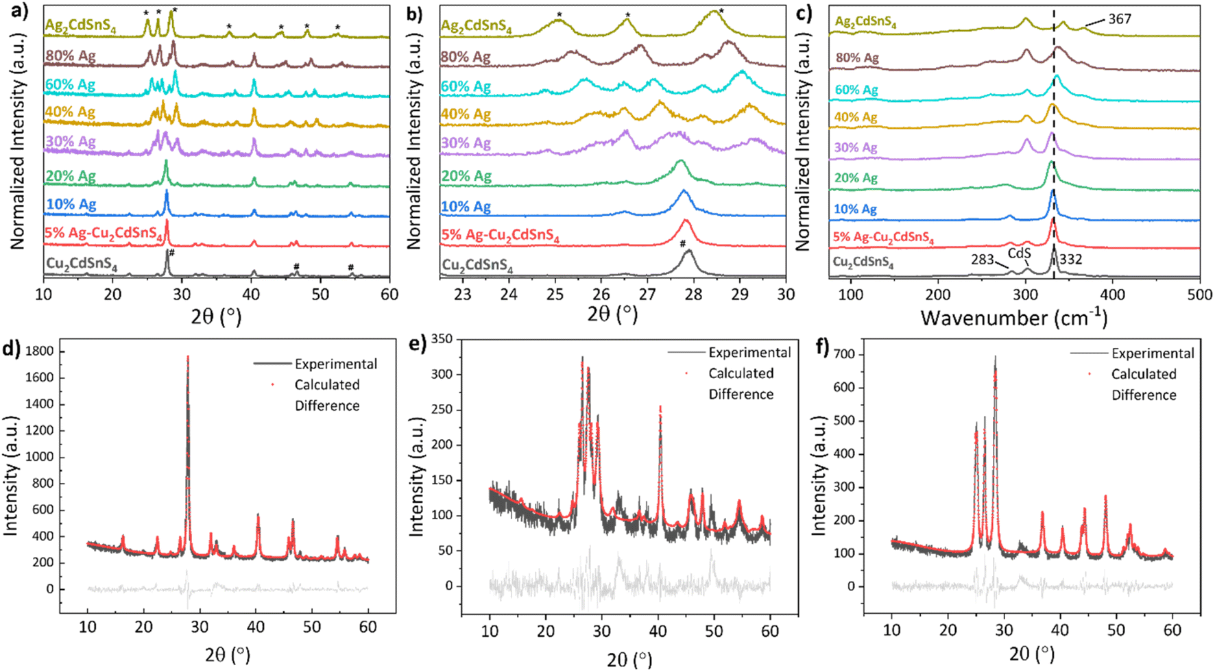 | ||
| Fig. 1 (a) X-ray diffraction (XRD) pattern and (c) Raman spectra of Cu2CdSnS4 film with various Ag content and Ag2CdSnS4 film. (b) Magnified XRD view on 23–30° diffraction angle near (112) peak of Cu2CdSnS4; the intensities in (a–c) are normalized, % Ag refers to the concentration ratio of Ag/Ag + Cu. (d) Refinement plot for Cu2CdSnS4 sample, (e) 30% Ag of (Cu1−xAgx)2CdSnS4 sample, and (f) Ag2CdSnS4 sample. | ||
To identify the presence of secondary phases, Raman measurement for all films were conducted as shown in Fig. 1c. Under 532 nm excitation wavelength, the Cu2CdSnS4 film exhibits its characteristics symmetry modes at 332 and 283 cm−1, similar to previously reported Raman data.16,17 The appearance of these two peaks dominates up to 20% Ag. Note that the CdS secondary phase can also be identified in the spectra, especially at the 30–80% Ag films, where the film quality seems to deteriorate. On the other hand, no Cu2SnS3 secondary phase (290 and 350 cm−1) is detected on all films. At the higher amount of Ag (≥60%), the main peak at 332 cm−1 shifts to a higher wavenumber value, and the appearance of a shoulder peak at 367 cm−1 suggests a change in the phase from the stannite Cu2CdSnS4 to orthorhombic Ag2CdSnS4. Although to our knowledge Raman studies about Ag2CdSnS4 have not been reported, K. Pietak et al. presented in their study of Ag2ZnSnS4 similar results regarding their Raman measurements with the appearance of an intense peak at 341 cm−1 as well as an additional peak at 370 cm−1.30 In addition to our XRD, it seems that the observed Raman peaks phase belongs to orthorhombic Ag2CdSnS4, the first time it has been reported in the literature.
The transition between Cu2CdSnS4 into Ag2CdSnS4 was also quantitively studied by Rietveld refinement of the XRD spectra. All films have been refined to their tetragonal unit cells for Cu2CdSnS4, orthorhombic for Ag2CdSnS4, and both for the partial Cu–Ag substitution. The value of Rbragg evaluates how well each phase fits with the model, the lower, the better. The goodness of fit (GOF), representing the closeness of the refinement model to the actual measured data with one as the ideal value, is used to determine the refinement model quality. The GOF equation is shown below,
The refinement for pure Cu2CdSnS4 sample can be closely fitted (Rbragg = 3.79; GOF = 1.53) to the calculated tetragonal unit cells, as shown in Fig. 1d. This fitting case still applies after adding 5% up to 20% Ag (Fig. S1†). At 30% Ag, the experimental data shown in Fig. 1e cannot be reasonably fitted to tetragonal Cu2CdSnS4 (Rbragg = 5.27) or orthorhombic Ag2CdSnS4 (Rbragg = 9.66). Finally, the 80% Ag (Rbragg = 2.72; GOF = 1.47) and pure Ag2CdSnS4 (Rbragg = 2.95; GOF = 1.46) data have a close fit to the calculated orthorhombic unit cells, as shown in Fig. 1f and S1.†
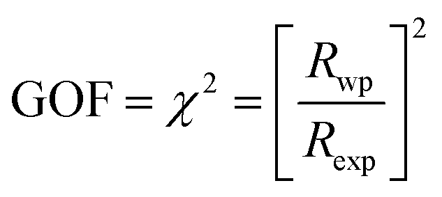
Following, the study on film morphology (Fig. 2) is carried out. Pure Cu2CdSnS4 and the Ag-alloyed films have large and compact grains with up to a 10% Ag concentration ratio. Meanwhile, the grains become smaller and less uniform between 20% and 40% Ag. While the presence of grain boundaries could be benign for high efficiency Cu(In,Ga)Se2 thin film solar cells due to the effective passivation by alkali,32,33 in general for polycrystalline material, such as the more closely related Cu2ZnSnS4, grain boundaries may introduce additional deep level states within the energy bandgap acting as effective recombination centre.34,35 The grains become more uniform as the Ag content increases to 60%. Finally, the Ag2CdSnS4 film has uniform grains, albeit smaller than the Cu2CdSnS4 film. This means the uniform grains that could benefit a solar cell device can be obtained from pure Cu2CdSnS4 and Ag2CdSnS4 film, as well as the 5% Ag.
 | ||
| Fig. 2 Surface SEM images for (a) Cu2CdSnS4 and additional Ag content of (b) 5%, (c) 10%, (d) 20%, (e) 30%, (f) 40%, (g) 60%, (h) 80%, and for (i) Ag2CdSnS4. | ||
The elemental ratios of the films were measured by EDS, as shown in Table S1.† All the films have non-stoichiometric Cu-poor and Cd-rich compositions similar to the as-prepared solutions. The Ag concentration in each variation is in good agreement with the prepared amount. A line scan was conducted for 5% and 30% Ag films to check the elemental distribution of the film. Ag is distributed uniformly throughout both films, similar to other cations, as shown in Fig. S2.† Thus, there is no Ag distribution grading for both the small and mixed phases concentrations.
Optoelectronic properties of (Cu1−xAgx)2CdSnS4
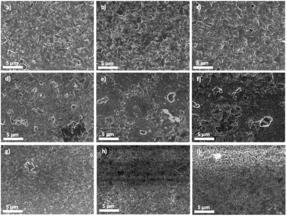
UV-Vis was conducted for all concentrations to understand further the optoelectronic properties of the (Cu1−xAgx)2CdSnS4 films. The increased bandgap for (Cu1−xAgx)2CdSnS4 in Fig. 3a and S3† can be attributed to the higher incorporation of Ag, as demonstrated by the peaks shifting observed from XRD. The absorption edge for pure Cu2CdSnS4 and small concentrations of Ag up to 10% are quite sharp, indicating their better light absorption ability, while it is less so for 20% Ag and 30% Ag. At 30% Ag, the mixed phases clearly contributed to the less sharp absorption edge. This observation is the same for higher Ag concentrations, but for pure Ag2CdSnS4, a clear, sharp absorption edge comparable to Cu2CdSnS4 and Cu2ZnSnS4 can be obtained with an extracted bandgap of 1.93 eV. | ||
| Fig. 3 (a) Tauc plot of (αhv)2 as a function of hv for Cu2ZnSnS4 and (Cu1−xAgx)2CdSnS4 films; (b) apparent carrier concentration and (c) mobility extracted from Hall film measurement for (Cu1−xAgx)2CdSnS4 with various Ag concentrations. | ||
Hall measurement is then conducted for all concentrations of the (Cu1−xAgx)2CdSnS4 films. The apparent carrier concentration for Cu2CdSnS4 is 2.7 × 1015 cm−3 with carrier mobility of 0.44 cm2 V−1 s−1. The presence of mixed phases from 30% to 80% Ag could affect the values of their carrier density, as there is no clear correlation between carrier concentration and mobility values to the Ag concentrations, as observed in Fig. 3. Interestingly, the doping type changes between p-type for Cu2CdSnS4 into n-type for Ag2CdSnS4. The high formation energy of its acceptor defects could be the reason for this transition, as similarly observed in Ag2ZnSnS4 and Ag2ZnSnSe4.11,12
The highest peaks obtained from photoluminescence spectra in Fig. S4a† do not represent the bandgaps of all the samples. However, secondary peaks around 1.35 eV close to each respective bandgap value of 5% and 10% Ag films were observed, indicating fewer defects or improved quality after small doping of Ag. The main peaks for higher concentrations of Ag (30%, 60%, and pure Ag2CdSnS4) were all blue-shifted corresponding to their higher bandgaps.
Photovoltaic properties of (Cu1−xAgx)2CdSnS4
The complete device configuration is SLG/Mo/(Cu1−xAgx)2CdSnS4/CdS/ITO without anti-reflection coating. I–V measurements were conducted on at least ten devices for each Ag concentration to obtain statistical representation. The photovoltaic parameters for the devices up to 60% Ag are presented in Fig. 4. Between 0% to 10% Ag, there is no significant improvement in FF and VOC. The performance starts to drop at 20% Ag concentration, accompanied by a drop in JSC and FF, which can be related to the presence of non-uniform grains and voids on the film. The presence of mixed phases between 30% and 40% Ag is well-reflected in the device performance. While for 30% Ag, the VOC is comparable with lesser Ag concentration, at 40%, the VOC drops significantly.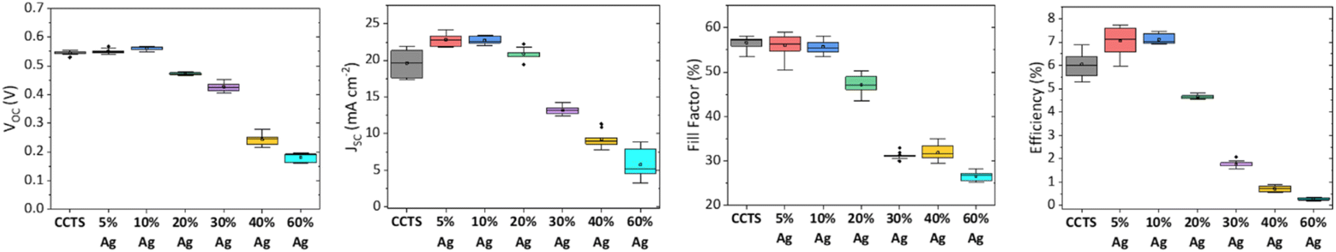 | ||
| Fig. 4 Device parameters for Cu2CdSnS4 with various Ag concentrations. All boxplots represent ten devices each. | ||
Both 30% and 40% of Ag devices have poor FF and JSC. The presence of pinholes might be responsible for the poor VOC and FF at those concentrations. At the same time, the JSC also suffers from carrier recombination at the grain boundaries due to poor grain growth on top of the increasing bandgap. The devices have very poor performance when Ag content is higher than Cu at 60%, which could be attributed to the much higher bandgap affecting the band alignment with the CdS layer. Moreover, despite improved morphology conditions at 80% and 100% Ag, an alternative device configuration might be necessary to conform to the n-type majority carriers' condition, as observed in Fig. 3. Lastly, we did not obtain a working Ag2CdSnS4 device because the remaining pure phase is n-type at this concentration.
The External Quantum Efficiency (EQE) for the best-performing devices up to 60% Ag concentration is shown in Fig. 5a. Poor EQE results were obtained for Ag concentrations above 60%. The JSC improvement for 5% and 10% Ag devices is well-reflected by each device's higher EQE values, which is translated to the higher integrated JSC values. For 5% Ag, the EQE increases throughout the whole wavelength. This improvement can be attributed to the reduced recombination at the bulk of Cu2CdSnS4 due to small Ag content doping.36 Similar improvement is observed from the 10% Ag, but there is a reduction at the lower wavelength, probably due to parasitic absorption of the top layers from CdS/ITO.37 The higher Ag contents are consistent between JSC values and the EQE. At higher concentrations, the bandgap increases to 1.63 eV for 60% Ag. This increasing trend is also obtained from the extracted bandgap values from the absorption spectra in Fig. S3.† Moreover, this is also consistent with the experimentally observed 1.93 eV bandgap for pure Ag2CdSnS4.38
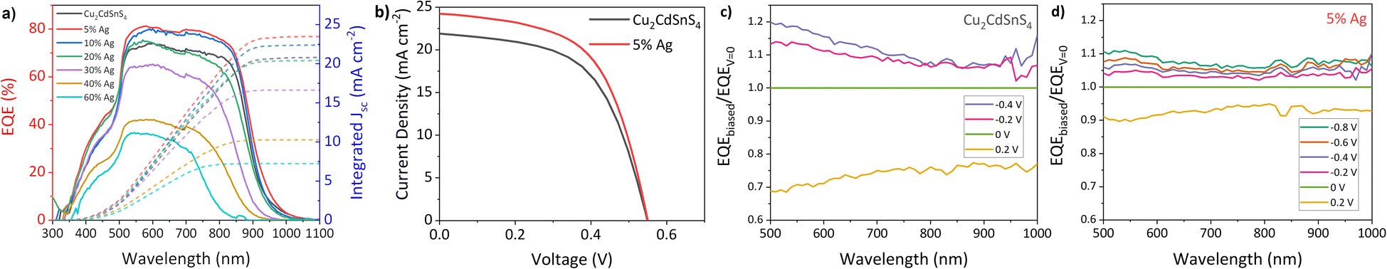 | ||
| Fig. 5 (a) External quantum efficiency (EQE) curves (left axis) and their integrated JSC (right axis-dashes) for Cu2CdSnS4 with various Ag concentrations, (b) I–V curves for the best Cu2CdSnS4 and 5% Ag device. Voltage-biased EQE curves for (c) Cu2CdSnS4 and (d) 5% Ag device normalized to the unbiased EQE values. | ||
The improvement for the best device with 5% Ag mainly comes from slightly higher JSC and Fill Factor (FF) compared to the pure Cu2CdSnS4 devices, as observed in Table 1 and Fig. 5b. The better FF for the 5% Ag device is in good agreement with its lower Rs and Gsh value. The same JSC improvement for the small amount of Ag was also observed in CZTS devices with a high Cd substitution concentration. It was attributed to larger grain sizes and enhanced depletion width.9
| Device | V OC [mV] | J SC [mA cm−2] | FF [%] | η [%] | E g [eV] | n | J 01 [×10−6 A cm−2] | R s [Ω cm2] | G sh [mS cm−2] |
|---|---|---|---|---|---|---|---|---|---|
| Cu2CdSnS4 | 549 | 21.89 | 57.16 | 6.87 | 1.39 | 2.35 | 2.23 | 2.55 | 3.93 |
| 5% Ag | 550 | 24.23 | 57.89 | 7.72 | 1.41 | 2.64 | 6.64 | 1.63 | 3.79 |
To further understand the reason for the improved performance of the 5% Ag device, we performed a C–V measurement. Comparing the pure Cu2CdSnS4 and 5% Ag devices, as shown in Fig. S5,† the extracted carrier concentration for these devices does not significantly change, as similarly observed from Hall measurement (Table S2†). The amount of Ag might be too small to significantly affect the carrier density. Nevertheless, the 5% Ag device shows a slight improvement in its depletion width, leading to a better carrier collection, as reflected by its superior EQE. We also performed EQE measurements under positive and negative voltage bias for the two devices, as shown in Fig. 5c and d. The EQEbiased/EQEV=0 ratio indicates severe interface recombination in Cu2CdSnS4. In particular, the large deviation of this ratio from the ideal value of 1 and the corresponding slope of the dependence of this ratio on wavelength suggests the presence of interface recombination.36 Adding 5% Ag to Cu2CdSnS4 brings this ratio closer to 1, suggesting that interface recombination in these devices is suppressed to some extent. The 5% Ag device performance improvement can be mainly attributed to this reason and the better film quality as demonstrated by the presence of a PL peak at the energy level close to its bandgap value.
The EQE spectrum onset for Cu2CdSnS4 and 5% Ag devices was further analyzed by evaluating its derivative d(−ln(1 − EQE))/dE as presented in Fig. S6† referring to previous methods in the literature.39,40 According to Mattheis et al.,39 the standard deviation of the Gaussian fitting of the derivative d(−ln(1 − EQE))/dE represents the amplitude of bandgap fluctuations (σEg). For the 5% Ag device, the σEg value of 56 meV is not far from the σEg value of the Cu2CdSnS4 device (58 meV). However, these values are much smaller than our similarly processed Cu2ZnSnS4 solar cell device (116 meV) and comparable to the σEg value of the current 13.8% record efficiency Cu2ZnSn(S,Se)4 (CZTSSe) solar cell device, which is about 52 meV.41 As the degree of bandgap fluctuations has been associated with the 2CuCd + SnCd (or 2CuZn + SnZn) deep defects,3,16,42 the small σEg values of Cu2CdSnS4 and 5% Ag devices indicate the suppression of the associated deep defects. A combination of this work and the use of Sn4+ precursors (used in the 13.8% CZTSSe device and currently regarded as essential for high-efficiency CZTSSe solar cells) might give better CCTS device performance in future studies.
Conclusions
In this work, we have investigated Ag substitution on Cu2CdSnS4 and monotonically studied its transition. The phase transition from tetragonal Cu2CdSnS4 to orthorhombic Ag2CdSnS4 starts at 30% Ag concentration, as observed from the XRD spectra. Despite the bigger ionic radii size (Ag 1.00 Å vs. Cu 0.60 Å, Cd 0.78 Å), higher Ag concentrations do not effectively translate into better photovoltaic performance. This is demonstrated by its poor crystal quality, optoelectronic properties, and possible carrier-type changes. However, the n-type nature of the fully-substituted Ag2CdSnS4 might require a different device configuration and further optimization to obtain a working solar cell device. On the other hand, small amounts of Ag concentrations of up to 10% have improved device performance compared to pure Cu2CdSnS4. The 5% Ag device has the best performance of 7.72%, which is attributed to its better film quality and superior interface properties, leading to its higher JSC compared to the pure Cu2CdSnS4.Author contributions
A. I. fabricated the (Cu1−xAgx)2CdSnS4 thin films, conducted XRD and its Rietveld analysis, carried out SEM-EDS, UV-Vis, Hall measurement and solar cell device characterization, and analyzed the raw data. S. L. helped with the analysis of solar cell device characterization and Hall measurement results. J. M. R. T. contributed suggestions on the synthesis. R. S. performed the PL measurements, EQE-V, and helped with the analysis of the results (supervised by R. A.). A. G. M. conducted Raman measurement and helped with the discussion of the result (supervised by E. S.). S. H. contributed suggestions on EQE-V data. L. H. W. supervised the work.Conflicts of interest
There are no conflicts to declare.Acknowledgements
The authors would like to acknowledge the funding support from the CREATE Programme under the Campus for Research Excellence and Technological Enterprise (CREATE), which is supported by the National Research Foundation, Prime Minister's Office, Singapore, and the Ministry of Education (MOE) Tier 2 Project (MOE-T2EP50120-0008). Also, we would like to acknowledge the Facility for Analysis, Characterisation, Testing and Simulation (FACTS), Nanyang Technological University, Singapore, for use of their X-ray facilities.References
- S. Giraldo, Z. Jehl, M. Placidi, V. Izquierdo-Roca, A. Pérez-Rodríguez and E. Saucedo, Progress and Perspectives of Thin Film Kesterite Photovoltaic Technology: A Critical Review, Adv. Mater., 2019, 31, 1–18 CrossRef PubMed.
- S. Hadke, M. Huang, C. Chen, Y. F. Tay, S. Chen, J. Tang and L. Wong, Emerging Chalcogenide Thin Films for Solar Energy Harvesting Devices, Chem. Rev., 2022, 122, 10170–10265 CrossRef CAS PubMed.
- S. Chen, A. Walsh, X. G. Gong and S. H. Wei, Classification of lattice defects in the kesterite Cu2ZnSnS4 and Cu2ZnSnSe4 earth-abundant solar cell absorbers, Adv. Mater., 2013, 25, 1522–1539 CrossRef CAS PubMed.
- J. Fu, Q. Tian, Z. Zhou, D. Kou, Y. Meng, W. Zhou and S. Wu, Improving the Performance of Solution-Processed Cu2ZnSn(S,Se)4 Photovoltaic Materials by Cd2+ Substitution, Chem. Mater., 2016, 28, 5821–5828 CrossRef CAS.
- R. Sun, D. Zhuang, M. Zhao, Q. Gong, M. Scarpulla, Y. Wei, G. Ren and Y. Wu, Beyond 11% efficient Cu2ZnSn(Se,S)4 thin film solar cells by cadmium alloying, Sol. Energy Mater. Sol. Cells, 2018, 174, 494–498 CrossRef CAS.
- C. Yan, K. Sun, J. Huang, S. Johnston, F. Liu, B. P. Veettil, K. Sun, A. Pu, F. Zhou, J. A. Stride, M. A. Green and X. Hao, Beyond 11% Efficient Sulfide Kesterite Cu2ZnxCd1-xSnS4 Solar Cell: Effects of Cadmium Alloying, ACS Energy Lett., 2017, 2, 930–936 CrossRef CAS.
- Z. Su, J. M. R. Tan, X. Li, X. Zeng, S. K. Batabyal and L. H. Wong, Cation Substitution of Solution-Processed Cu2ZnSnS4 Thin Film Solar Cell with over 9% Efficiency, Adv. Energy Mater., 2015, 5, 1500682 CrossRef.
- A. Guchhait, Z. Su, Y. F. Tay, S. Shukla, W. Li, S. W. Leow, J. M. R. Tan, S. Lie, O. Gunawan and L. H. Wong, Enhancement of Open-Circuit Voltage of Solution-Processed Cu2ZnSnS4 Solar Cells with 7.2% Efficiency by Incorporation of Silver, ACS Energy Lett., 2016, 1, 1256–1261 CrossRef CAS.
- S. H. Hadke, S. Levcenko, S. Lie, C. J. Hages, J. A. Márquez, T. Unold and L. H. Wong, Synergistic Effects of Double Cation Substitution in Solution-Processed CZTS Solar Cells with over 10% Efficiency, Adv. Energy Mater., 2018, 8, 1802540 CrossRef.
- C. Ma, H. Guo, K. Zhang, N. Yuan and J. Ding, Fabrication of p-type kesterite Ag2ZnSnS4 thin films with a high hole mobility, Mater. Lett., 2017, 186, 390–393 CrossRef CAS.
- T. Gershon, K. Sardashti, O. Gunawan, R. Mankad, S. Singh, Y. S. Lee, J. A. Ott, A. Kummel and R. Haight, Photovoltaic Device with over 5% Efficiency Based on an n-Type Ag2ZnSnSe4 Absorber, Adv. Energy Mater., 2016, 6, 1601182 CrossRef.
- H. Guo, C. Ma, K. Zhang, X. Jia, Y. Li, N. Yuan and J. Ding, The fabrication of Cd-free Cu2ZnSnS4-Ag2ZnSnS4 heterojunction photovoltaic devices, Sol. Energy Mater. Sol. Cells, 2018, 178, 146–153 CrossRef CAS.
- S. Lie, M. Guc, V. Tunuguntla, V. Izquierdo-Roca, S. Siebentritt and L. H. Wong, Comprehensive physicochemical and photovoltaic analysis of different Zn substitutes (Mn, Mg, Fe, Ni, Co, Ba, Sr) in CZTS-inspired thin film solar cells, J. Mater. Chem. A, 2022, 9137–9149 RSC.
- L. Choubrac, G. Brammertz, N. Barreau, L. Arzel, S. Harel, M. Meuris and B. Vermang, 7.6% CZGSe Solar Cells Thanks to Optimized CdS Chemical Bath Deposition, Phys. Status Solidi, 2018, 215, 1800043 CrossRef.
- L. Choubrac, M. Bär, X. Kozina, R. Félix, R. G. Wilks, G. Brammertz, S. Levcenko, L. Arzel, N. Barreau, S. Harel, M. Meuris and B. Vermang, Sn Substitution by Ge: Strategies to Overcome the Open-Circuit Voltage Deficit of Kesterite Solar Cells, ACS Appl. Energy Mater., 2020, 3, 5830–5839 CrossRef CAS.
- S. Hadke, S. Levcenko, G. Sai Gautam, C. J. Hages, J. A. Márquez, V. Izquierdo-Roca, E. A. Carter, T. Unold and L. H. Wong, Suppressed Deep Traps and Bandgap Fluctuations in Cu2CdSnS4 Solar Cells with ≈8% Efficiency, Adv. Energy Mater., 2019, 9, 1902509 CrossRef CAS.
- P. Fan, J. Lin, J. Hu, Z. Yu, Y. Zhao, S. Chen, Z. Zheng, J. Luo, G. Liang and Z. Su, Over 10% Efficient Cu2CdSnS4 Solar Cells Fabricated from Optimized Sulfurization, Adv. Funct. Mater., 2022, 32, 2207470 CrossRef CAS.
- Y. E. Romanyuk, S. G. Haass, S. Giraldo, M. Placidi, D. Tiwari, D. J. Fermin, X. Hao, H. Xin, T. Schnabel, M. Kauk-Kuusik, P. Pistor, S. Lie and L. H. Wong, Doping and alloying of kesterites, JPhys Energy, 2019, 1, 044004 CrossRef CAS.
- C. Yan, J. Huang, K. Sun, S. Johnston, Y. Zhang, H. Sun, A. Pu, M. He, F. Liu, K. Eder, L. Yang, J. M. Cairney, N. J. Ekins-Daukes, Z. Hameiri, J. A. Stride, S. Chen, M. A. Green and X. Hao, Cu2ZnSnS4 solar cells with over 10% power conversion efficiency enabled by heterojunction heat treatment, Nat. Energy, 2018, 3, 764–772 CrossRef CAS.
- L. Meng, Y. Li, B. Yao, Z. H. Ding, G. Yang, R. J. Liu, R. Deng and L. Liu, Mechanism of effect of intrinsic defects on electrical and optical properties of Cu2CdSnS4: An experimental and first-principles study, J. Phys. D Appl. Phys., 2015, 48, 445105 CrossRef.
- K. Timmo, M. Altosaar, M. Pilvet, V. Mikli, M. Grossberg, M. Danilson, T. Raadik, R. Josepson, J. Krustok and M. Kauk-Kuusik, The effect of Ag alloying of Cu2(Zn,Cd)SnS4 on the monograin powder properties and solar cell performance, J. Mater. Chem. A, 2019, 7, 24281–24291 RSC.
- S. Saidi, S. Zriouel, L. B. Drissi and M. Maaroufi, First principles study of electronic and optical properties of Ag2CdSnS4 chalcogenides for photovoltaic applications, Comput. Mater. Sci., 2018, 152, 291–299 CrossRef CAS.
- T. Küllmey, J. Hein, E. M. Heppke, I. Efthimiopoulos and B. Paulus, High-Pressure Behavior and Disorder for Ag2ZnSnS4 and Ag2CdSnS4, ACS Omega, 2021, 6, 27387–27395 CrossRef PubMed.
- E. M. Heppke, S. Berendts and M. Lerch, Crystal structure of mechanochemically synthesized Ag2 CdSnS4, Z. Naturforsch., B, 2020, 75, 393–402 CrossRef CAS.
- Y.-F. Qi, D.-X. Kou, W.-H. Zhou, Z.-J. Zhou, Q.-W. Tian, Y.-N. Meng, X.-S. Liu, Z.-L. Du and S.-X. Wu, Engineering of interface band bending and defects elimination via a Ag-graded active layer for efficient (Cu,Ag)2ZnSn(S,Se)4 solar cells, Energy Environ. Sci., 2017, 10, 2401–2410 RSC.
- W.-C. Huang, S.-Y. Wei, C.-H. Cai, W.-H. Ho and C.-H. Lai, The role of Ag in aqueous solution processed (Ag,Cu)2ZnSn(S,Se)4 kesterite solar cells: antisite defect elimination and importance of Na passivation, J. Mater. Chem. A, 2018, 6, 15170–15181 RSC.
- Y. Qi, Y. Liu, D. Kou, W. Zhou, Z. Zhou, Q. Tian, S. Yuan, Y. Meng and S. Wu, Enhancing Grain Growth for Efficient Solution-Processed (Cu,Ag)2ZnSn(S,Se)4 Solar Cells Based on Acetate Precursor, ACS Appl. Mater. Interfaces, 2020, 12, 14213–14223 CrossRef CAS PubMed.
- Y. Qi, X. Zhao, Y. Liu, D. Kou, W. Zhou, Z. Zhou, S. Yuan, Y. Meng and S. Wu, Synergistic effect of Mn on bandgap fluctuations and surface electrical characteristics in Ag-based Cu2ZnSn(S,Se)4 solar cells, J. Mater. Chem. A, 2021, 9, 2292–2300 RSC.
- R. D. Shannon, Revised effective ionic radii and systematic studies of interatomic distances in halides and chalcogenides, Acta Crystallogr., Sect. A, 1976, 32, 751–767 CrossRef.
- K. Pietak, C. Jastrzebski, K. Zberecki, D. J. Jastrzebski, W. Paszkowicz and S. Podsiadlo, Synthesis and structural characterization of Ag2ZnSnS4 crystals, J. Solid State Chem., 2020, 290, 2–7 CrossRef.
- R. A. Young, The Rietveld Method, Oxford University Press, 1995 Search PubMed.
- C. S. Jiang, R. Noufi, J. A. AbuShama, K. Ramanathan, H. R. Moutinho, J. Pankow and M. M. Al-Jassim, Local built-in potential on grain boundary of Cu(In,Ga)Se2 thin films, Appl. Phys. Lett., 2004, 84, 3477–3479 CrossRef CAS.
- N. Nicoara, R. Manaligod, P. Jackson, D. Hariskos, W. Witte, G. Sozzi, R. Menozzi and S. Sadewasser, Direct evidence for grain boundary passivation in Cu(In,Ga)Se2 solar cells through alkali-fluoride post-deposition treatments, Nat. Commun., 2019, 10, 1–8 CrossRef CAS PubMed.
- J. Li, D. B. Mitzi and V. B. Shenoy, Structure and electronic properties of grain boundaries in earth-abundant photovoltaic absorber Cu2ZnSnSe4, ACS Nano, 2011, 5, 8613–8619 CrossRef CAS PubMed.
- J. Li, J. Huang, F. Ma, H. Sun, J. Cong, K. Privat, R. F. Webster, S. Cheong, Y. Yao, R. L. Chin, X. Yuan, M. He, K. Sun, H. Li, Y. Mai, Z. Hameiri, N. J. Ekins-Daukes, R. D. Tilley, T. Unold, M. A. Green and X. Hao, Unveiling microscopic carrier loss mechanisms in 12% efficient Cu2ZnSnSe4 solar cells, Nat. Energy, 2022, 7, 754–764 CrossRef CAS.
- Y. F. Tay, S. S. Hadke, M. Zhang, N. Lim, S. Y. Chiam and L. H. Wong, Improving the interfacial properties of CZTS photocathodes by Ag substitution, J. Mater. Chem. A, 2020, 8, 8862–8867 RSC.
- W. Wang, M. T. Winkler, O. Gunawan, T. Gokmen, T. K. Todorov, Y. Zhu and D. B. Mitzi, Device characteristics of CZTSSe thin-film solar cells with 12.6% efficiency, Adv. Energy Mater., 2014, 4, 1–5 Search PubMed.
- G. E. Davydyuk, G. L. Myronchuk, I. V. Kityk, S. P. Danyl’Chuk, V. V. Bozhko and O. V. Parasyuk, Ag2CdSnS4 single crystals as promising materials for optoelectronic, Opt. Mater., 2011, 33, 1302–1306 CrossRef CAS.
- J. Mattheis, U. Rau and J. H. Werner, Light absorption and emission in semiconductors with band gap fluctuations-A study on Cu(In,Ga)Se2 thin films, J. Appl. Phys., 2007, 101, 113519 CrossRef.
- U. Rau, B. Blank, T. C. M. Müller and T. Kirchartz, Efficiency Potential of Photovoltaic Materials and Devices Unveiled by Detailed-Balance Analysis, Phys. Rev. Appl., 2017, 7, 1–9 Search PubMed.
- J. Zhou, X. Xu, H. Wu, J. Wang, L. Lou, K. Yin, Y. Gong, J. Shi, Y. Luo, D. Li, H. Xin and Q. Meng, Control of the phase evolution of kesterite by tuning of the selenium partial pressure for solar cells with 13.8% certified efficiency, Nat. Energy, 2023, 8, 526–535 CrossRef CAS.
- G. Rey, G. Larramona, S. Bourdais, C. Choné, B. Delatouche, A. Jacob, G. Dennler and S. Siebentritt, On the origin of band-tails in kesterite, Sol. Energy Mater. Sol. Cells, 2018, 179, 142–151 CrossRef CAS.
Footnote |
| † Electronic supplementary information (ESI) available. See DOI: https://doi.org/10.1039/d3ta04529c |
| This journal is © The Royal Society of Chemistry 2024 |