
 Open Access Article
 This Open Access Article is licensed under a Creative Commons Attribution-Non Commercial 3.0 Unported Licence
Engineering of the perovskite/electron-transporting layer interface with transition metal chalcogenides for improving the performance of inverted perovskite solar cells†
Dimitris
Tsikritzis
 ab,
Konstantinos
Chatzimanolis
a,
Nikolaos
Tzoganakis
a,
Konstantinos
Rogdakis
ab,
Marilena Isabella
Zappia
c,
Beatriz
Martín-García
def,
Ahmad
Bagheri
cd,
Hossein
Beydaghi
c,
Lukáš
Děkanovský
g,
Zdeněk
Sofer
g,
Sebastiano
Bellani
c,
Francesco
Bonaccorso
cd and
Emmanuel
Kymakis
ab
ab,
Konstantinos
Chatzimanolis
a,
Nikolaos
Tzoganakis
a,
Konstantinos
Rogdakis
ab,
Marilena Isabella
Zappia
c,
Beatriz
Martín-García
def,
Ahmad
Bagheri
cd,
Hossein
Beydaghi
c,
Lukáš
Děkanovský
g,
Zdeněk
Sofer
g,
Sebastiano
Bellani
c,
Francesco
Bonaccorso
cd and
Emmanuel
Kymakis
ab
aDepartment of Electrical & Computer Engineering, Hellenic Mediterranean University (HMU), Heraklion 71410, Crete, Greece. E-mail: kymakis@hmu.gr
bInstitute of Emerging Technologies (i-EMERGE) of HMU Research Center, Heraklion 71410, Crete, Greece
cBeDimensional S.p.A., Via Lungotorrente Secca 30R, 16163 Genova, Italy
dGraphene Labs, Istituto Italiano di Tecnologia, Via Morego, 30, 16163, Genova, Italy
eCIC NanoGUNE BRTA, 20018 Donostia-San Sebastián, Basque Country, Spain
fIKERBASQUE, Basque Foundation for Science, 48009 Bilbao, Spain
gDepartment of Inorganic Chemistry, University of Chemistry and Technology Prague, Technická 5, 166 28 Prague 6, Czech Republic
First published on 3rd April 2024
Abstract
Layered two-dimensional (2D) transition-metal chalcogenides (TMCs) attract substantial interest across multiple disciplines due to their unique properties. In perovskite solar cells (PSCs), researchers have extensively explored the integration of 2D TMCs to enhance device power conversion efficiency (PCE) and stability. However, there is a research gap in understanding their impact on inverted (p–i–n) PSCs, especially at the perovskite/electron-transporting layer (ETL) interface. This study addresses this gap by investigating the effect of inserting InSe, MoSe2, and SnS2 nanosheets at the perovskite/ETL interface in inverted PSCs. The introduction of 2D TMC interlayers induces a downward shift in perovskite energy levels, optimizing the energy level alignment at the perovskite/ETL interface and substantially increasing the PCE. The SnS2-incorporating PSCs exhibit the highest relative improvement of 5.05% (InSe and MoSe2 nanosheets yield 3.37% and 2.5% PCE increase, respectively). This enhancement results in an absolute PCE of 18.5% with a fill factor exceeding 82%. Furthermore, the incorporation of InSe nanosheets eliminates the burn-in phase enhancing the long-term stability (T70 of 250 h) of unencapsulated devices. This study underscores the significant improvement in PSCs' PCE and stability by selectively incorporating suitable TMCs at the perovskite/ETL interface. This research offers insights into the potential role of TMCs in advancing PSCs.
Introduction
Transition metal chalcogenides (TMCs) represent a highly promising class of materials with a wide range of applications. These materials exhibit exceptional optical, electrical, catalytic, and mechanical properties, making them suitable for numerous fields, including batteries,1,2 supercapacitors,3, (photo)catalysis,4–8, (photo)transistors9–11 and other optoelectronic devices.12–17 One feature of TMCs is their band gap tunability, which makes them ideal for adjustable light absorption, e.g., serving as the photoactive layer in photovoltaic applications. However, photovoltaic devices using TMC-based photoactive layers currently exhibit insufficient power conversion efficiency (PCE) just above 5%.18,19 When integrated with other photoactive layers as interlayers or additives, TMCs have been reported to enhance the performance of solar cells by finely tuning specific device characteristics, ultimately improving the overall performance.20 For instance, MoS2 has been successfully integrated into both Si-based21,22 and organic solar cells,23 improving significantly the cell performance. The role of TMCs depends specifically on photovoltaic technologies, for each of which a systematic investigation of the role of TMCs is required for reliable advancements in this field.24In this context, the incorporation of TMCs, typically in their two-dimensional (2D) forms (i.e., nanosheets), in perovskite solar cells (PSCs) has been investigated in various studies.24–26 In particular, MoS2 was deposited on the perovskite in normal (n–i–p) PSCs, acting as an interlayer between the perovskite and the hole-transporting layer (HTL) to enhance the device PCE and stability by improving the hole extraction processes and offering a physical barrier against ion migration from the metal contact to the perovskite and vice versa.27–29 In a similar study, MoSe2 nanosheets were also screened together with MoS2 ones to form thin interlayers between the perovskite and the HTL in normal PSC structures, enhancing the performance of reference devices.30–32 MoS2 was also used in combination with graphene-incorporating electron transporting layers (ETLs) and MXene-incorporating perovskites, testifying the effectiveness of 2D material interface engineering.33,34 Also, TMCs have been proposed as charge-transporting layers to completely replace conventional materials of PSCs.24,35 Specifically, MoS2 and WS2 were used as HTLs in inverted PSCs showing similar PCEs to the references based on poly(3,4-ethylenedioxythiophene):poly(styrenesulfonate) (PEDOT:PSS).36,37 SnS2 was used as the ETL in PSCs, improving the PCE up to 20%.38 Despite its n-type behavior, MoSe2 was used as an HTL in an inverted PSC,39 showing a high PCE of 18%. The mixing of PEDOT:PSS with MoS2, as well as other dichalcogenides, was used to increase the PCE of inverted PSCs.40–42 Dichalcogenides, including MoS2, but also other TMCs, have also been proposed to modify the electron-transporting layer (ETL)/metal electrode interface, aiming at creating favorable energy level alignments to efficiently collect photogenerated electrons.26,43–45
Despite the tremendous progress recently achieved by incorporating MoS2 in PSCs, including the realization of the world's first perovskite solar farm operating for several months,46 other representative TMCs for photovoltaic applications, based on the above consideration, are SnS2, MoSe2, as well as monochalcogenides, e.g., InSe.24 While MoS2 is mainly used to improve the hole extraction efficiency in n–i–p PSCs, there are other TMCs that may play a relevant role in promoting the electron extraction from the perovskite to the current collectors. In particular, SnS2 is an n-type layered semiconductor with a tunable band gap ranging from 2.1 to 3.4 eV, depending on the number of its layers. In its bulk form, SnS2 has already been established in photovoltaic applications.47 Meanwhile, the exfoliation of SnS2 into 2D few-layer nanosheets has been achieved through both chemical48 and physical methods.49 Extensive characterization of SnS2 has revealed that its monolayer possesses an indirect bandgap equal to 2.033 eV, while its field-effect transistor (FET) mobility was estimated to be in the range of 5 cm2 V−1 s−1 to 250 cm2 V−1 s−1,50 enabling the realization of ultrathin FETs and logic gates.49 Also, SnS2 shows a high electron density of ∼6 × 10⁻¹⁹ cm−3,48 justifying its use as an effective dopant for PC70BM in inverted PSCs.51 In this context, the high conductivity of 2D SnS2 has been leveraged for the fabrication of ultra-thin ETLs in PSCs.38,52 The valence band maximum (VB) and conduction band minimum (CB) of 2D SnS2 have been estimated through ultraviolet photoelectron spectroscopy (UPS) to be −6.54 and −4.24 eV, respectively, indicating their potential ability to collect electrons from common perovskite active layers.38
MoSe2 shows a similar structure to that of MoS2 (2H phase). MoSe2 is a semiconductor with an indirect band gap of 1.41 eV.53 However, few-layer MoSe2 exhibits a direct band gap of 1.58 eV (ref. 53 and 54) and a FET electron mobility of 50–250 cm2 V−1 s−1.55 Thin-films of 2D MoSe2 have been used in photovoltaics,56,57 catalysis for the hydrogen evolution reaction,58,59 and energy storage systems.60,61
Finally, InSe is a III–VI layered compound made of stacked quaternary layers of Se–In–In–Se atoms that are held together by van der Waals interactions. Consequently, bulk InSe can be exfoliated into 2D forms by means of various methods, including scalable liquid-phase exfoliation (LPE) techniques.62–64 InSe is generally considered as an n-type semiconductor and it was shown through experimental and theoretical studies that a band gap transition from direct to indirect occurs when InSe layer thickness reduces below 6 nm.65 Also, its bandgap can increase from ∼1.2 eV for the bulk to 1.4 eV for few-layers InSe66 and up to 2.1 eV for a monolayer of InSe.67 The electron affinity was found to be −4.55 eV and the work function (WF) to be 5.1 eV for bulk InSe.68 The Hall mobility of InSe nanosheets was estimated to be ∼103 cm2 V−1 s−1 at room temperature (RT)69 and the carrier density was measured to be ∼1013 cm−2.70 Pioneering studies also demonstrated n-type FETs based on 2D InSe, with an electron mobility at room temperature (RT) on the order of 103 cm2 V−1 s−1.71 This electron mobility is higher than those achieved by other high mobility 2D semiconducting materials, including MoS2. Based on its properties, 2D InSe has been used in photovoltaic devices,72,73 as well as for (photo)electrochemical water splitting reactions,64 photodetectors,63,74 sensors,75 thermoelectric devices,76 and spintronic devices.77
Overall, the above discussed TMCs represent interesting 2D materials for the engineering of the perovskite/ETL interface, aiming at improving the device PCE. Most studies on incorporating TMCs in PSCs have been focused on the optimization of the perovskite/HTL interface. To the best of our knowledge, there is no systematic work on engineering the perovskite/ETL interface with TMCs. In this study, we aim to fill this research gap by studying representative TMCs, i.e., SnS2, MoSe2 and InSe, to optimize the perovskite/ETL interface in inverted PSCs. Selected TMCs, exfoliated through LPE, were deposited over the perovskite layer using solution processing, ensuring the scalability and industrialization feasibility of our interface engineering approach. The insertion of TMCs between the perovskite layer and the PC70BM effectively aligns the energy levels of the materials, enabling an efficient electron extraction from the perovskite to the current collector. This research aims to contribute to the extension of current 2D material interface engineering strategies to PSCs, providing new insights into the application of TMCs in inverted PSCs. The findings of this study have implications on the development of high-performance solar cells and can boost the utilization of TMCs in large-scale solar energy production, as already demonstrated for 2D MoS2.46
Results
The methods of bulk TMC synthesis and exfoliation, and those for characterization of the exfoliated TMCs, are reported in the ESI.† In particular, bulk 2H-MoSe2, 2H-SnS2 and β-InSe were exfoliated through ultrasonication-assisted LPE in isopropyl alcohol (IPA),78,79 followed by sedimentation-based separation (SBS) to remove unexfoliated crystals from the exfoliated material.59,80Fig. 1a, d and g show the transmission electron microscopy (TEM) images of representative nanosheets of MoSe2, SnS2 and InSe, respectively. Fig. S1† reports the statistical analysis of the lateral size of the nanosheets. The lateral size data approximately follow log-normal distributions, with modes of 52.9 nm, 99.1 nm, and 143.9 nm for MoSe2, SnS2 and InSe nanosheets, respectively. Fig. 1b, e and h report the XRD patterns recorded for MoSe2, SnS2 and InSe nanosheets, respectively, comparing them with those measured for the bulk counterparts. The positions of the diffraction peaks of the exfoliated samples resemble those of the bulk counterparts, well-matching with the patterns of their hexagonal phases, i.e., 2H-MoSe2, P![[6 with combining macron]](https://www.rsc.org/images/entities/char_0036_0304.gif) m2 space group, JCPDS card no. 029-0914; 2H-SnS2, P63mc space group, JCPDS card no. 023-0677; β-InSe structure, P63/mmc space group, JCPDS card no. 034-1431. Bulk crystals show the diffraction peaks belonging to the {00l} family, which means that they are aligned along the (001) plane perpendicular to the c axis. Compared to the bulk materials, MoSe2 and InSe nanosheets exhibit additional XRD peaks, likely due to their disordered arrangements. SnS2 nanosheets, instead, preserve a placement perpendicular to their c axis. The broadening of the XRD peaks in the exfoliated materials indicate that their crystal sizes decreased after the LPE process. Fig. 1c, f and i report the Raman spectra of the bulk and exfoliated materials, exhibiting the characteristic Raman modes expected for each material by the group theory.81–83 In MoSe2 nanosheets, the redshift of the A1g peak compared to the same peak of the bulk counterpart is explained by the softening of the vibrational mode with decreasing the crystal thickness.84,85 The Raman spectrum of bulk SnS2 shows two phonon modes at ∼313 cm−1 (A1g) and ∼203 cm−1 (Eg), as well as a weak two-phonon scattering signal of A1g-LA (M) (Fig. 1f).86 After exfoliation, additional peaks appear and are likely associated with by-products, e.g., oxides.87 Finally, bulk and exfoliated InSe exhibit various Raman peaks at similar positions, i.e., A11g at ∼116 cm−1, E21g at ∼177 cm−1, E12g at ∼199 cm−1, A2u at ∼208 cm−1, and A21g at ∼227 cm−1, which is consistent with previous studies.63,64
m2 space group, JCPDS card no. 029-0914; 2H-SnS2, P63mc space group, JCPDS card no. 023-0677; β-InSe structure, P63/mmc space group, JCPDS card no. 034-1431. Bulk crystals show the diffraction peaks belonging to the {00l} family, which means that they are aligned along the (001) plane perpendicular to the c axis. Compared to the bulk materials, MoSe2 and InSe nanosheets exhibit additional XRD peaks, likely due to their disordered arrangements. SnS2 nanosheets, instead, preserve a placement perpendicular to their c axis. The broadening of the XRD peaks in the exfoliated materials indicate that their crystal sizes decreased after the LPE process. Fig. 1c, f and i report the Raman spectra of the bulk and exfoliated materials, exhibiting the characteristic Raman modes expected for each material by the group theory.81–83 In MoSe2 nanosheets, the redshift of the A1g peak compared to the same peak of the bulk counterpart is explained by the softening of the vibrational mode with decreasing the crystal thickness.84,85 The Raman spectrum of bulk SnS2 shows two phonon modes at ∼313 cm−1 (A1g) and ∼203 cm−1 (Eg), as well as a weak two-phonon scattering signal of A1g-LA (M) (Fig. 1f).86 After exfoliation, additional peaks appear and are likely associated with by-products, e.g., oxides.87 Finally, bulk and exfoliated InSe exhibit various Raman peaks at similar positions, i.e., A11g at ∼116 cm−1, E21g at ∼177 cm−1, E12g at ∼199 cm−1, A2u at ∼208 cm−1, and A21g at ∼227 cm−1, which is consistent with previous studies.63,64
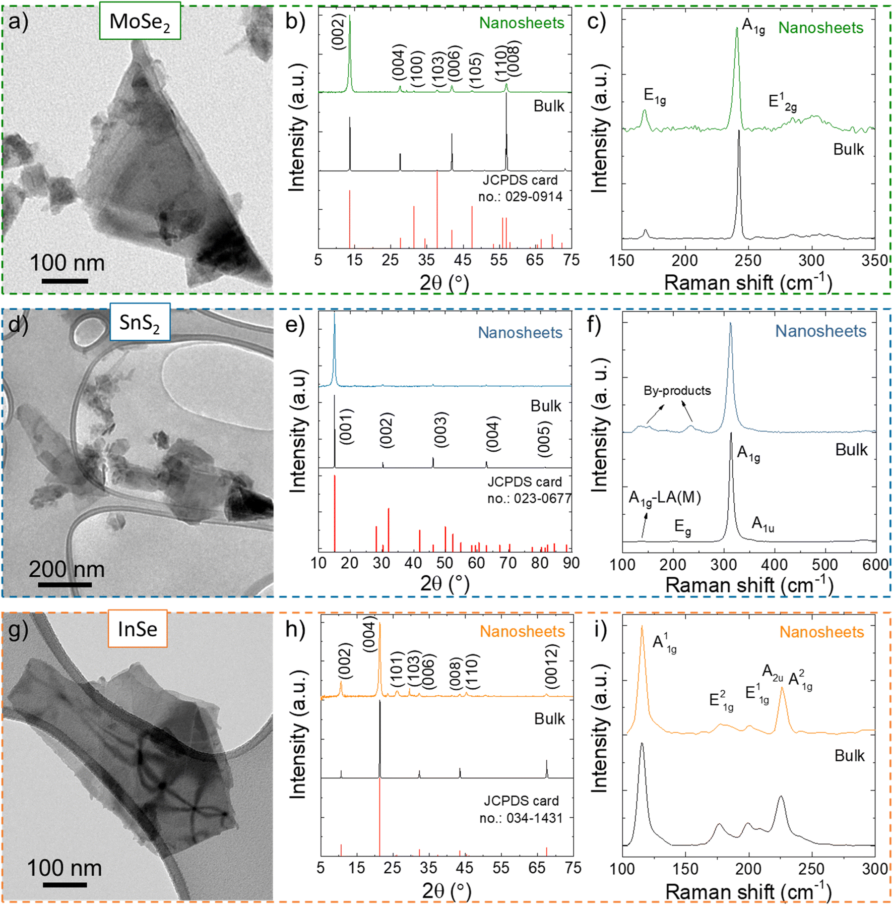 | ||
| Fig. 1 TEM images, XRD patterns and Raman spectra measured for (a–c) MoSe2, (d–f) SnS2 and (g–i) InSe nanosheets. The XRD patterns and Raman spectra of bulk counterparts are also shown for comparison. | ||
The deposition of TMC nanosheets was carried out by spin coating their dispersion (formulated in chlorobenzene) onto the perovskite layer. Successive spin coating steps were applied to optimize the interlayer of TMC nanosheets at the perovskite/PC70BM interface. The formation of ultrathin 2D TMC films on the surface of the perovskites was assessed through X-ray photoelectron spectroscopy (XPS) and scanning electron microscopy (SEM) measurements. As shown in Fig. S2,† the 3d In, Mo, and Sn XPS spectra, acquired on the perovskite surfaces treated with 2D TMCs, confirm the presence of InSe, MoSe2 and SnS2 nanosheets, respectively. Fig. S3† presents top-view SEM images of the perovskite surface treated with 2D TMCs. The images show scattered TMC nanosheets atop the perovskite surface, without the presence of large material aggregates. Importantly, the few-layer nature of the exfoliated TMCs permits nanometer-thick interlayers to be obtained without resulting in significant changes of the surface topography of the underlying perovskite film.
The effect of the 2D TMC interlayers between the perovskite and PC70BM layers was evaluated by measuring the device performance estimated through the analysis of their J–V curves under 1 sun illumination. Fig. S4–S6† report the statistical analysis of the photovoltaic parameters, i.e., PCE, open circuit voltage (Voc), fill factor (FF) and short circuit current (Jsc), for the investigated devices, produced with different 2D TMC interlayers and by varying the number of successive spin coating steps used for the deposition of 2D TMCs atop the perovskite. These data indicate that the number of spin coating steps has a significant impact on the final photovoltaic parameters of the devices. Specifically, exceeding two spin coating steps has a detrimental effect on the device performance. This negative effect is likely associated with the excessive exposure of the perovskite layer to the solvent of 2D TMC dispersions. Importantly, the incorporation of 2D TMCs into the device structure through one or two spin coating steps always increases the PCE of the device. In addition, different 2D TMC interlayers result in the improvement of specific photovoltaic parameters, indicating different beneficial effects of the investigated materials. To compare the devices that have different 2D TMC interlayers and to eliminate any uncontrollable effect between various fabrication batches, Fig. 2 plots the percentage relative change of PCE and of the other photovoltaic parameters measured for the most performing 2D TMC-incorporating PSCs compared to reference (without 2D TMCs) devices. Cells incorporating InSe and SnS2 nanosheets exhibit a similar behavior, characterized by a substantial increase in their FF by 2.32% and 2.83%, respectively, along with a slight improvement in Jsc, and no change in Voc, compared to the reference device. Differently, the device containing MoSe2 nanosheets exhibits a decrease in FF by about 1.9% compared to the reference cell. Meanwhile the Jsc increases considerably by 2.95% and the Voc increases by 1.42% compared to the reference cell. Notably, the devices incorporating SnS2 nanosheets demonstrated the greatest relative PCE improvement of 5.05%, with a 2.83% increase in FF, resulting in a PCE as high as 18.5% and FF of 82%. Fig. S7† shows the external quantum efficiency spectrum of the best device.
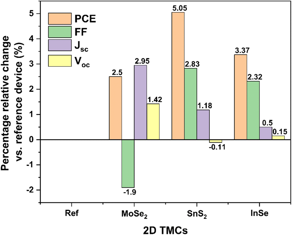 | ||
| Fig. 2 Percentage relative change of PCE, FF, Voc, and Jsc of 2D TMC-incorporating PSCs compared to reference (without 2D TMCs) PSCs. | ||
The optoelectronic properties of the perovskite surface treated with 2D TMCs were investigated to assess if they are correlated with the device photovoltaic parameters. The WF and valence band (VB) maximum energy of the perovskite surface were estimated using ambient photoemission spectroscopy measurements. Fig. S8† illustrates the WF measurements of the perovskite surface before and after the deposition of 2D TMCs, and the extrapolated WF values are listed in Table 1. The WF of the pristine perovskite was determined to be 4.15 eV and increased after depositing the 2D TMCs (i.e., 4.8 eV after SnS2 nanosheet deposition). This behavior suggests the presence of a surface dipole that shifts the perovskite vacuum level to higher energies, with the negative part of the dipole facing outward from the surface (positive part facing toward the perovskite). The value of the interface dipole, Δ, for each case is listed in Table 1. Fig. S9† shows the VB measurements for the investigated samples. Interestingly, compared to the untreated perovskite, the presence of 2D TMCs shifts the perovskite VB to lower energy. Fig. 3 reports the sketch of the energy level diagram expected for the investigated cell configurations. The incorporation of 2D TMCs alters the energy level alignment at the interfaces between the perovskite and the PC70BM. Specifically, the conduction band (CB) minimum energy and VB maximum energy shift to lower values. Thus, the CB minimum energy of the perovskite approaches that of PC70BM, while the VB maximum energy of the perovskite moves away from that of PTAA. To quantify the offset of the energy levels, the energy difference between the CB minimum energies (conduction band offset-CBO) and the difference between the VB maximum energies (valence band offset-VBO) of the respective charge transporting layers and the perovskite were evaluated. In greater detail, the CBO and VBO can be calculated as:
| CBO = χperovskite − χPCBM | (1) |
| VBO = χPTAA + Eg,PTAA − (χperovskite + Eg,perovskite) | (2) |
| Perovskite | W F (eV) | Δ (eV) | VB (eV) | CB (eV) | CBO (eV) | VBO (eV) |
|---|---|---|---|---|---|---|
| Reference | −4.15 | −5.41 | −3.82 | −0.08 | −0.01 | |
| InSe | −4.46 | 0.31 | −5.49 | −3.9 | 0.00 | −0.09 |
| SnS2 | −4.82 | 0.67 | −5.47 | −3.88 | −0.02 | −0.07 |
| MoSe2 | −4.73 | 0.58 | −5.52 | −3.93 | 0.03 | −0.12 |
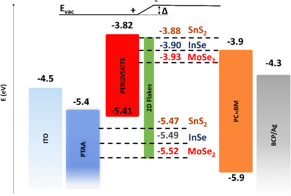 | ||
| Fig. 3 Sketch of the energy level diagram of the investigated devices (energy values are not in scale). The dashed lines show the energy levels of the perovskite after the deposition of InSe, SnS2, and MoSe2 nanosheets. | ||
The measured values for VB maximum energies and the calculated values for CBO and VBO are listed in Table 1. For the reference device, the CBO is negative (−0.08 eV), indicating that the CB minimum energy of PC70BM is lower than that of the perovskite. This energy level alignment at the perovskite/PC70BM interface is commonly indicated as a “cliff,” signifying the absence of an energy barrier for electron injection from the perovskite to the PC70BM. Similarly, the VBO for the reference device is −0.01 eV, implying no injection barrier for holes at the PTAA/perovskite interface. However, the CBO and VBO change drastically upon the deposition of 2D TMCs atop the perovskite. The CBO is reduced to −0.02 eV after the deposition of SnS2 nanosheets and becomes 0.00 eV after depositing InSe nanosheets. Conversely, the CBO is positive (0.03 eV) when MoSe2 nanosheets are deposited atop the perovskite, resulting in the formation of a “spike” feature at the perovskite/PC70BM interface.
In our previous work, we have demonstrated that the doping of the perovskite with BiTeI nanosheets leads to a modification of the energy levels of the perovskite.88 In this context, increasing the CBO and decreasing the VBO have proven to be advantageous for device performance. Similar to our previous findings, tuning the CBO and VBO by incorporating TMC interlayers enhances the FF and, thus, the PCE of PSCs, as demonstrated for PSCs containing InSe and SnS2 nanosheets. In the case of MoSe2-containing PSCs, the formation of a “spike” level alignment at the interface is also expected to enhance the FF. However, a decrease in FF was observed together with an increase in Voc, suggesting a different behavior of MoSe2 nanosheets compared to SnS2 and InSe nanosheets. The VBO of the reference sample (−0.01 eV) decreases to −0.12 eV with the incorporation of the MoSe2 interlayer. Our previous work has demonstrated that lowering the VBO is advantageous for device performance, as it reduces nonradiative recombination at the interface between the HTL (PTAA) and the perovskite.88 Moreover, experimental and theoretical studies have emphasized the importance of an absolute energy level offset of approximately 0.2 eV at the PTAA/perovskite interface.89 Additionally, a VBO between 0 and −0.18 eV has been identified as the optimum range for efficient hole extraction.90 Therefore, the observed improvement in Voc for MoSe2 can be attributed to the reduced recombination at the PTAA/perovskite interface, as the incorporation of MoSe2 helps to tune the VBO closer to the theoretically optimum range. The improved PCE of devices incorporating InSe can be attributed to the tendency of this material to oxidize under ambient conditions, forming In2O3. Notably, the surface of InSe readily undergoes oxidation when subjected to air heat treatment.91–93 The native oxide In2O3 is an n-type semiconductor with an optical band gap of 3.66 eV92 and a high carrier concentration of approximately 6 × 1019 cm−3,68,94 which can improve device PCE. Theoretical studies have indicated that H2O, N2, and O2 molecules physisorbed onto the 2D InSe surface, resulting in partial electron charge transfer from InSe to the adsorbed molecules.95 Additionally, it has been shown that a monolayer of InSe readily physisorbs H2O under ambient conditions, irrespective of the presence of In or Se vacancies. Depending on the vacancies, InSe can be doped with H2O, leading to either p-type (In vacancies) or n-type (Se vacancies) behavior,96 suggesting precaution to assess the actual role of the InSe interlayers. The interface dipole at the interface of perovskite/ETL could reduce interface recombination, by preventing electron carriers in the ETL from reaching the interface.
The incorporation of 2D TMCs atop the perovskite has been the subject of extensive research, and our findings supplement previous studies, mainly focused on dichalcogenides and normal PSCs. Indeed, we have observed a strong agreement between our results and a theoretical study investigating the perovskite/InSe interface,97 in which it was shown that InSe plays a crucial role in facilitating electron charge transport, causing charge transfer from the perovskite towards the InSe. In line with this, we have observed that the WF of the perovskite surface covered with InSe nanosheets is higher than that of the control sample, indicating the accumulation of negative charge on the top surface with InSe, forming an interface dipole, as well as for the other investigated 2D TMCs.97 Furthermore, experimental evidence has shown that the interfaces of TMCs such as MoS2, WSe2, and MoSe2 with inorganic perovskites exhibit ultrafast and efficient charge carrier transfer.98,99 Based on these findings, it is expected that the presence of 2D TMCs on the perovskite will not impede charge transport, a hypothesis that is confirmed by our experimental results. Moreover, SnS2 nanosheets have been utilized in the literature to form the ETL, enhancing charge extraction and passivating interfacial traps more efficiently compared to SnO2.38 Our results are aligned with this, further supporting the beneficial effects of SnS2 as an ETL in PSCs. Consequently, our study provides additional insights on the incorporation of the 2D TMC interlayer at the perovskite/PC70BM interface, highlighting their potential in improving charge extraction in PSCs.
Lifetime measurements
The stability of the PSCs incorporating TMC nanosheets was investigated following the International Summit on Organic Photovoltaic Stability (ISOS) L-2 protocol. Thus, the devices were subjected to continuous 1 sun illumination under ambient humidity at 65 °C.100Fig. 4 illustrates the normalized PCE of the unencapsulated devices over time. The reference device exhibited a burn-in phase during the initial testing period and a fast degradation afterwards. This behavior can be attributed to the degradation of the Ag electrode caused by its reaction with iodine, which migrated from the perovskite layer.101–103 The device incorporating SnS2 nanosheets showed the worst stability, while the one containing MoSe2 nanosheets exhibited similar behavior to the reference cell. On the other hand, the incorporation of InSe led to the disappearance of the burn-in phase, enhancing the cell stability. The InSe-incorporating PSC exhibited a T70 of 250 h, i.e., the device retained 70% of its initial PCE after 250 h. The superior stability of the InSe-containing PSC compared to the other cells can be correlated with the morphological and chemical properties of InSe nanosheets. The photo-induced degradation of InSe towards In2Se3 and In2O3 under ambient conditions can commence a surface passivation interlayer at the perovskite/ETL interface. The formation of In2Se3 and In2O3 (ref. 104) does not seem to affect the PCE and enhances the stability of the device, according to our results. Moreover, the InSe nanosheets show the highest lateral size amongst the investigated flakes (Fig. S1†) and therefore, InSe can serve as an effective barrier, protecting the metal electrode from the degradation species of the perovskite, thus enhancing the device stability.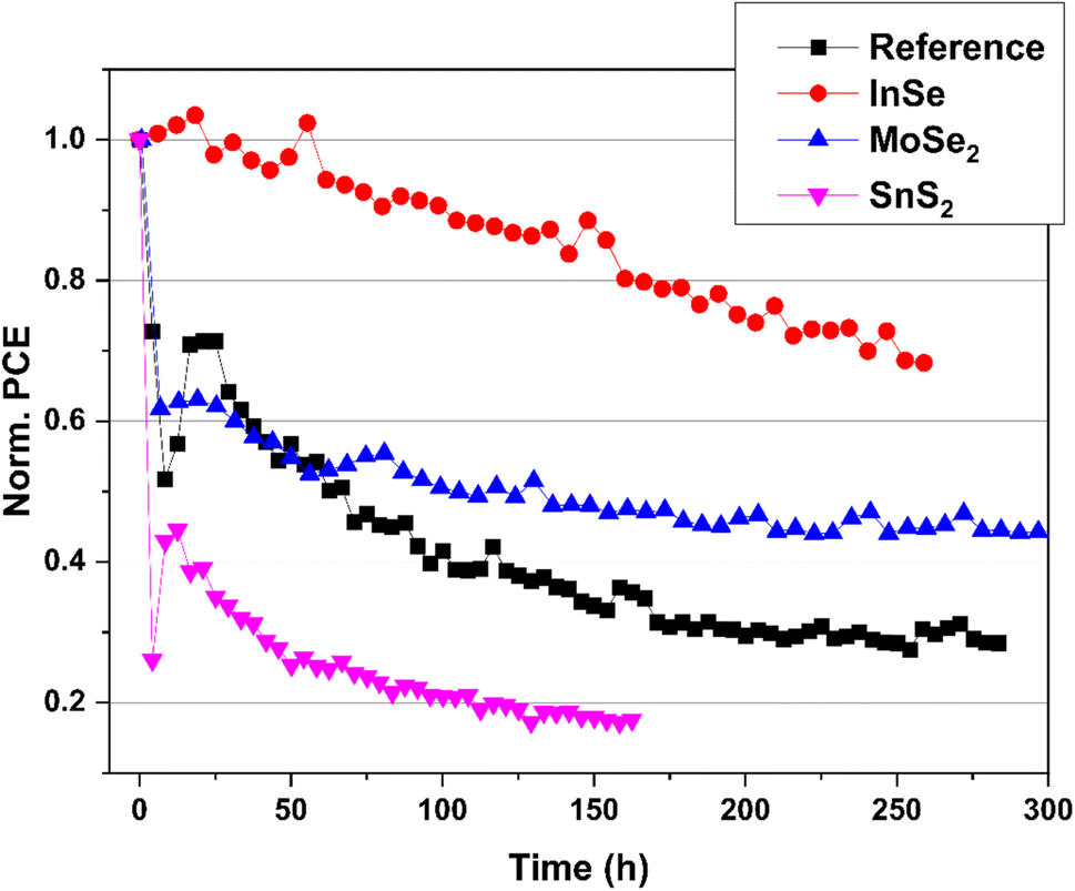 | ||
| Fig. 4 Stability measurements of the PSCs incorporating InSe, MoSe2, and SnS2 interlayers under continuous 1 sun illumination, ambient humidity and 65 °C temperature (ISOS L-2). | ||
Conclusions
The structure of inverted PSCs has been systematically optimized by screening the incorporation of various 2D TMCs in the form of an interlayer between the perovskite and the PC70BM ETL. Specifically, bulk InSe, SnS2, and MoSe2 were exfoliated by means of ultrasonication-assisted LPE and deposited atop the perovskite surface by spin coating to form thin (nanometer-thick) films. The incorporation of TMC interlayers causes a shift in the energy levels towards lower energies, altering the energy level offset at perovskite/charge-transporting layer interfaces. In detail, the introduction of SnS2 and InSe nanosheets reduces the energy offset at the perovskite/PC70BM interface, resulting in an increase of the FF and PCE of the devices. The SnS2- and InSe-incorporating devices exhibited relative improvement in PCE by 5.05% and 3.37%, respectively, compared to reference (without 2D TMCs) cells. The PSCs engineered with the SnS2 interlayer showed the highest PCE, reaching 18.5% and FF of 82%. Conversely, the MoSe2 interlayer introduces a small cliff arrangement at the interface of perovskite/PC70BM. Compared to reference cells, the cells of MoSe2-incorporating devices demonstrated improved PCE compared to reference cells, increasing the Jsc and Voc. Moreover, to assess the long-term stability of the cells, the devices were subjected to continuous 1 sun illumination at 65 °C, following the ISOS-L2 ageing protocol. The results indicate different stability behaviors of the cells incorporating the investigated TMC interlayers, reflecting the different physico-chemical properties of the 2D TMCs. The incorporation of the MoSe2 interlayer has no discernible effect on device stability, while the SnS2 interlayer has a negative impact. On the other hand, InSe interlayer eliminates the burn-in degradation observed in the reference devices, significantly improving the overall cell stability. In summary, this work elucidates the potential of 2D TMCs to engineer the architecture of inverted PSCs.Conflicts of interest
There are no conflicts of interest to declare.Acknowledgements
We thank the Microelectronic Research Group at the University of Crete and Aleka Manousaki for the SEM images of the perovskite films, and Dr Manolis Spanakis from the Materials Science and Technology Department of the University of Crete, for the XPS measurements. The work has been supported by the European Union's Horizon Europe Framework Programme for research and innovation under grant agreement no. 694101—2D-PRINTABLE and by the European Union's Horizon 2020 research and innovation program under the Project EMERGE. The EMERGE project has received funding under grant agreement no. 101008701. Z. S. was supported by the ERC-CZ program (project LL2101) from the Ministry of Education Youth and Sports (MEYS) and used large infrastructure from project reg. no. CZ.02.1.01/0.0/0.0/15_003/0000444 financed by the EFRR.References
- S. Bellani, F. Wang, G. Longoni, L. Najafi, R. Oropesa-Nuñez, A. E. D. R. Castillo, M. Prato, X. Zhuang, V. Pellegrini, X. Feng and F. Bonaccorso, WS2–Graphite Dual-Ion Batteries, Nano Lett., 2018, 18(11), 7155–7164 CrossRef CAS
.
- H. Beydaghi, S. Bellani, L. Najafi, R. Oropesa-Nuñez, G. Bianca, A. Bagheri, I. Conticello, B. Martín-García, S. Kashefi, M. Serri, L. Liao, Z. Sofer, V. Pellegrini and F. Bonaccorso, Sulfonated NbS2-based proton-exchange membranes for vanadium redox flow batteries, Nanoscale, 2022, 14(16), 6152–6161 RSC
- A. Bagheri, S. Bellani, H. Beydaghi, M. Eredia, L. Najafi, G. Bianca, M. I. Zappia, M. Safarpour, M. Najafi, E. Mantero, Z. Sofer, G. Hou, V. Pellegrini, X. Feng and F. Bonaccorso, Functionalized Metallic 2D Transition Metal Dichalcogenide-Based Solid-State Electrolyte for Flexible All-Solid-State Supercapacitors, ACS Nano, 2022, 16(10), 16426–16442 CrossRef CAS PubMed
- L. Najafi, S. Bellani, R. Oropesa-Nuñez, B. Martín-García, M. Prato, L. Pasquale, J.-K. Panda, P. Marvan, Z. Sofer and F. Bonaccorso, TaS2, TaSe2, and Their Heterogeneous Films as Catalysts for the Hydrogen Evolution Reaction, ACS Catal., 2020, 10(5), 3313–3325 CrossRef CAS
- L. Najafi, S. Bellani, R. Oropesa-Nuñez, R. Brescia, M. Prato, L. Pasquale, C. Demirci, F. Drago, B. Martín-García, J. Luxa, L. Manna, Z. Sofer and F. Bonaccorso, Microwave-Induced Structural Engineering and Pt Trapping in 6R-TaS2 for the Hydrogen Evolution Reaction, Small, 2020, 16(50), 2003372 CrossRef CAS PubMed
- L. Najafi, R. Oropesa-Nuñez, S. Bellani, B. Martín-García, L. Pasquale, M. Serri, F. Drago, J. Luxa, Z. Sofer, D. Sedmidubský, R. Brescia, S. Lauciello, M. I. Zappia, D. V. Shinde, L. Manna and F. Bonaccorso, Topochemical Transformation of Two-Dimensional VSe2 into Metallic Nonlayered VO2 for Water Splitting Reactions in Acidic and Alkaline Media, ACS Nano, 2022, 16(1), 351–367 CrossRef CAS PubMed
- L. Najafi, S. Bellani, M. I. Zappia, M. Serri, R. Oropesa-Nuñez, A. Bagheri, H. Beydaghi, R. Brescia, L. Pasquale, D. V. Shinde, Y. Zuo, F. Drago, K. Mosina, Z. Sofer, L. Manna and F. Bonaccorso, Transition metal dichalcogenides as catalysts for the hydrogen evolution reaction: the emblematic case of ‘inert’ ZrSe2 as catalyst for electrolyzers, Nano Sel., 2022, 3(6), 1069–1081 CrossRef CAS
- E. D. Koutsouroubi, I. Vamvasakis, M. G. Minotaki, I. T. Papadas, C. Drivas, S. A. Choulis, G. Kopidakis, S. Kennou and G. S. Armatas, Ni-doped MoS2 modified graphitic carbon nitride layered hetero-nanostructures as highly efficient photocatalysts for environmental remediation, Appl. Catal., B, 2021, 297, 120419 CrossRef CAS
- S. Bellani, L. Najafi, A. Capasso, A. E. D. R. Castillo, M. R. Antognazza and F. Bonaccorso, Few-layer MoS2 flakes as a hole-selective layer for solution-processed hybrid organic hydrogen-evolving photocathodes, J. Mater. Chem. A, 2017, 5(9), 4384–4396 RSC
- L. Najafi, V. Romano, R. Oropesa-Nuñez, M. Prato, S. Lauciello, G. D’Angelo, S. Bellani and F. Bonaccorso, Hybrid Organic/Inorganic Photocathodes Based on WS2 Flakes as Hole Transporting Layer Material, Small Struct., 2021, 2(3), 2000098 CrossRef CAS
- D. N. Kouvatsos, G. Papadimitropoulos, T. Spiliotis, M. Vasilopoulou, D. Barreca, A. Gasparotto and D. Davazoglou, Electrical characteristics of vapor deposited amorphous MoS2 two-terminal structures and back gate thin film transistors with Al, Au, Cu and Ni-Au contacts, Phys. Status Solidi C, 2015, 12(7), 975–979 CrossRef CAS
- K. F. Mak and J. Shan, Photonics and optoelectronics of 2D semiconductor transition metal dichalcogenides, Nat. Photonics, 2016, 10(4), 216–226 CrossRef CAS
- M. I. Zappia, G. Bianca, S. Bellani, M. Serri, L. Najafi, R. Oropesa-Nuñez, B. Martín-García, D. Bouša, D. Sedmidubský, V. Pellegrini, Z. Sofer, A. Cupolillo and F. Bonaccorso, Solution-Processed GaSe Nanoflake-Based Films for Photoelectrochemical Water Splitting and Photoelectrochemical-Type Photodetectors, Adv. Funct. Mater., 2020, 30(10), 1909572 CrossRef CAS
- I. Kriegel, M. Ghini, S. Bellani, K. Zhang, A. W. Jansons, B. M. Crockett, K. M. Koskela, E. S. Barnard, E. Penzo, J. E. Hutchison, J. A. Robinson, L. Manna, N. J. Borys and P. J. Schuck, Light-Driven Permanent Charge Separation across a Hybrid Zero-Dimensional/Two-Dimensional Interface, J. Phys. Chem. C, 2020, 124(14), 8000–8007 CrossRef CAS
- G. Bianca, M. I. Zappia, S. Bellani, Z. Sofer, M. Serri, L. Najafi, R. Oropesa-Nuñez, B. Martín-García, T. Hartman, L. Leoncino, D. Sedmidubský, V. Pellegrini, G. Chiarello and F. Bonaccorso, Liquid-Phase Exfoliated GeSe Nanoflakes for Photoelectrochemical-Type Photodetectors and Photoelectrochemical Water Splitting, ACS Appl. Mater. Interfaces, 2020, 48598–48613 Search PubMed
- M. I. Zappia, G. Bianca, S. Bellani, N. Curreli, Z. Sofer, M. Serri, L. Najafi, M. Piccinni, R. Oropesa-Nuñez, P. Marvan, V. Pellegrini, I. Kriegel, M. Prato, A. Cupolillo and F. Bonaccorso, Two-Dimensional Gallium Sulfide Nanoflakes for UV-Selective Photoelectrochemical-type Photodetectors, J. Phys. Chem. C, 2021, 125(22), 11857–11866 CrossRef CAS PubMed
- G. Bianca, M. I. Zappia, S. Bellani, M. Ghini, N. Curreli, J. Buha, V. Galli, M. Prato, A. Soll, Z. Sofer, G. Lanzani, I. Kriegel and F. Bonaccorso, Indium Selenide/Indium Tin Oxide Hybrid Films for Solution-Processed Photoelectrochemical-Type Photodetectors in Aqueous Media, Adv. Mater. Interfaces, 2023, 10(1), 2201635 CrossRef CAS
- K. N. Nazif, A. Daus, J. Hong, N. Lee, S. Vaziri, A. Kumar, F. Nitta, M. E. Chen, S. Kananian, R. Islam, K.-H. Kim, J.-H. Park, A. S. Y. Poon, M. L. Brongersma, E. Pop and K. C. Saraswat, High-specific-power flexible transition metal dichalcogenide solar cells, Nat. Commun., 2021, 12(1), 7034 CrossRef PubMed
- S. Aftab, M. Z. Iqbal, S. Hussain, H. H. Hegazy and M. A. Saeed, Transition metal dichalcogenides solar cells and integration with perovskites, Nano Energy, 2023, 108, 108249 CrossRef CAS
- S. Das, D. Pandey, J. Thomas and T. Roy, The Role of Graphene and Other 2D Materials in Solar Photovoltaics, Adv. Mater., 2019, 31(1), 1802722 CrossRef PubMed
- T. He, C. Lan, S. Zhou, Y. Li, Y. Yin, C. Li and Y. Liu, Enhanced responsivity of a graphene/Si-based heterostructure broadband photodetector by introducing a WS2 interfacial layer, J. Mater. Chem. C, 2021, 9(11), 3846–3853 RSC
- Y. Tsuboi, F. Wang, D. Kozawa, K. Funahashi, S. Mouri, Y. Miyauchi, T. Takenobu and K. Matsuda, Enhanced photovoltaic performances of graphene/Si solar cells by insertion of a MoS2 thin film, Nanoscale, 2015, 7(34), 14476–14482 RSC
- G. Kakavelakis, A. E. Del Rio Castillo, V. Pellegrini, A. Ansaldo, P. Tzourmpakis, R. Brescia, M. Prato, E. Stratakis, E. Kymakis and F. Bonaccorso, Size-Tuning of WSe2 Flakes for High Efficiency Inverted Organic Solar Cells, ACS Nano, 2017, 11(4), 3517–3531 CrossRef CAS PubMed
- S. Bellani, A. Bartolotta, A. Agresti, G. Calogero, G. Grancini, A. Di Carlo, E. Kymakis and F. Bonaccorso, Solution-processed two-dimensional materials for next-generation photovoltaics, Chem. Soc. Rev., 2021, 50(21), 11870–11965 RSC
- L. C. Palilis, M. Vasilopoulou, A. Verykios, A. Soultati, E. Polydorou, P. Argitis, D. Davazoglou, A. R. b. M. Yusoff and M. K. Nazeeruddin, Inorganic and Hybrid Interfacial Materials for Organic and Perovskite Solar Cells, Adv. Energy Mater., 2020, 10(27), 2000910 CrossRef CAS
- D. Tsikritzis, K. Rogdakis, K. Chatzimanolis, M. Petrović, N. Tzoganakis, L. Najafi, B. Martín-García, R. Oropesa-Nuñez, S. Bellani, A. E. D. R. Castillo, M. Prato, M. M. Stylianakis, F. Bonaccorso and E. Kymakis, A two-fold engineering approach based on Bi2Te3 flakes towards efficient and stable inverted perovskite solar cells, Mater. Adv., 2020, 1(3), 450–462 RSC
- N. H. Hemasiri, S. Kazim and S. Ahmad, Reduced trap density and mitigating the interfacial losses by placing 2D dichalcogenide material at perovskite/HTM interface in a dopant free perovskite solar cells, Nano Energy, 2020, 77, 105292 CrossRef CAS
- A. Capasso, F. Matteocci, L. Najafi, M. Prato, J. Buha, L. Cinà, V. Pellegrini, A. D. Carlo and F. Bonaccorso, Few-Layer MoS2 Flakes as Active Buffer Layer for Stable Perovskite Solar Cells, Adv. Energy Mater., 2016, 6(16), 1600920 CrossRef
- L. Najafi, B. Taheri, B. Martín-García, S. Bellani, D. Di Girolamo, A. Agresti, R. Oropesa-Nuñez, S. Pescetelli, L. Vesce, E. Calabrò, M. Prato, A. E. D. R. Castillo, A. D. Carlo and F. Bonaccorso, MoS2 Quantum Dot/Graphene Hybrids for Advanced Interface Engineering of a CH3NH3PbI3 Perovskite Solar Cell with an Efficiency of over 20%, ACS Nano, 2018, 12(11), 10736–10754 CrossRef CAS
- M. Liang, A. Ali, A. Belaidi, M. I. Hossain, O. Ronan, C. Downing, N. Tabet, S. Sanvito, F. EI-Mellouhi and V. Nicolosi, Improving stability of organometallic-halide perovskite solar cells using exfoliation two-dimensional molybdenum chalcogenides, npj 2D Mater. Appl., 2020, 4(1), 40 CrossRef CAS
- Y. Busby, A. Agresti, S. Pescetelli, A. Di Carlo, C. Noel, J.-J. Pireaux and L. Houssiau, Aging effects in interface-engineered perovskite solar cells with 2D nanomaterials: a depth profile analysis, Mater. Today Energy, 2018, 9, 1–10 CrossRef
- G. Tang, P. You, Q. Tai, A. Yang, J. Cao, F. Zheng, Z. Zhou, J. Zhao, P. K. L. Chan and F. Yan, Solution-Phase Epitaxial Growth of Perovskite Films on 2D Material Flakes for High-Performance Solar Cells, Adv. Mater., 2019, 31(24), 1807689 CrossRef PubMed
- A. Agresti, S. Pescetelli, A. L. Palma, B. Martín-García, L. Najafi, S. Bellani, I. Moreels, M. Prato, F. Bonaccorso and A. Di Carlo, Two-Dimensional Material Interface Engineering for Efficient Perovskite Large-Area Modules, ACS Energy Lett., 2019, 4(8), 1862–1871 CrossRef CAS
- S. Pescetelli, A. Agresti, S. Razza, H. Pazniak, L. Najafi, F. Bonaccorso and A. D. Carlo, Synergic use of two-dimensional materials to tailor interfaces in large area perovskite modules, Nano Energy, 2022, 95, 107019 CrossRef CAS
- P. You, G. Tang and F. Yan, Two-dimensional materials in perovskite solar cells, Mater. Today Energy, 2019, 11, 128–158 CrossRef CAS
- Y. G. Kim, K. C. Kwon, Q. V. Le, K. Hong, H. W. Jang and S. Y. Kim, Atomically thin two-dimensional materials as hole extraction layers in organolead halide perovskite photovoltaic cells, J. Power Sources, 2016, 319, 1–8 CrossRef CAS
- B. Peng, G. Yu, Y. Zhao, Q. Xu, G. Xing, X. Liu, D. Fu, B. Liu, J. R. S. Tan, W. Tang, H. Lu, J. Xie, L. Deng, T. C. Sum and K. P. Loh, Achieving Ultrafast Hole Transfer at the Monolayer MoS2 and CH3NH3PbI3 Perovskite Interface by Defect Engineering, ACS Nano, 2016, 10(6), 6383–6391 CrossRef CAS PubMed
- X. Zhao, S. Liu, H. Zhang, S.-Y. Chang, W. Huang, B. Zhu, Y. Shen, C. Shen, D. Wang, Y. Yang and M. Wang, 20% Efficient Perovskite Solar Cells with 2D Electron Transporting Layer, Adv. Funct. Mater., 2019, 29(4), 1805168 CrossRef
- L.-C. Chen, Z.-L. Tseng, C.-C. Chen, S. H. Chang and C.-H. Ho, Fabrication and characteristics of CH3NH3PbI3 perovskite solar cells with molybdenum-selenide hole-transport layer, Appl. Phys. Express, 2016, 9(12), 122301 CrossRef
- Y. Choi, S. Jung, N. K. Oh, J. Lee, J. Seo, U. Kim, D. Koo and H. Park, Enhanced Charge Transport via Metallic 1T Phase Transition Metal Dichalcogenides-Mediated Hole Transport Layer Engineering for Perovskite Solar Cells, ChemNanoMat, 2019, 5(8), 1050–1058 CrossRef CAS
- D. Wang, N. K. Elumalai, M. A. Mahmud, H. Yi, M. B. Upama, R. A. L. Chin, G. Conibeer, C. Xu, F. Haque, L. Duan and A. Uddin, MoS2 incorporated hybrid hole transport layer for high performance and stable perovskite solar cells, Synth. Met., 2018, 246, 195–203 CrossRef CAS
- R. Dai, Y. Wang, J. Wang and X. Deng, Metal–Organic-Compound-Modified MoS2 with Enhanced Solubility for High-Performance Perovskite Solar Cells, ChemSusChem, 2017, 10(14), 2869–2874 CrossRef CAS PubMed
- M. Imran, H. Coşkun, F. H. Isikgor, L. Bichen, N. A. Khan and J. Ouyang, Highly efficient and stable inverted perovskite solar cells with two-dimensional ZnSe deposited using a thermal evaporator for electron collection, J. Mater. Chem. A, 2018, 6(45), 22713–22720 RSC
- Y. Wang, S. Wang, X. Chen, Z. Li, J. Wang, T. Li and X. Deng, Largely enhanced VOC and stability in perovskite solar cells with modified energy match by coupled 2D interlayers, J. Mater. Chem. A, 2018, 6(11), 4860–4867 RSC
- K. Chatzimanolis, K. Rogdakis, D. Tsikritzis, N. Tzoganakis, M. Tountas, M. Krassas, S. Bellani, L. Najafi, B. Martín-García, R. Oropesa-Nuñez, M. Prato, G. Bianca, I. Plutnarova, Z. Sofer, F. Bonaccorso and E. Kymakis, Inverted perovskite solar cells with enhanced lifetime and thermal stability enabled by a metallic tantalum disulfide buffer layer, Nanoscale Adv., 2021, 3(11), 3124–3135 RSC
- S. Pescetelli, A. Agresti, G. Viskadouros, S. Razza, K. Rogdakis, I. Kalogerakis, E. Spiliarotis, E. Leonardi, P. Mariani, L. Sorbello, M. Pierro, C. Cornaro, S. Bellani, L. Najafi, B. Martín-García, A. E. D. R. Castillo, R. Oropesa-Nuñez, M. Prato, S. Maranghi, M. L. Parisi, A. Sinicropi, R. Basosi, F. Bonaccorso, E. Kymakis and A. D. Carlo, Integration of two-dimensional materials-based perovskite solar panels into a stand-alone solar farm, Nat. Energy, 2022, 7(7), 597–607 CrossRef
- B. A. Parkinson, Dye sensitization of van der Waals surfaces of tin disulfide photoanodes, Langmuir, 1988, 4(4), 967–976 CrossRef CAS
- Y. Sun, H. Cheng, S. Gao, Z. Sun, Q. Liu, Q. Liu, F. Lei, T. Yao, J. He, S. Wei and Y. Xie, Freestanding Tin Disulfide Single-Layers Realizing Efficient Visible-Light Water Splitting, Angew. Chem., Int. Ed., 2012, 51(35), 8727–8731 CrossRef CAS PubMed
- D. De, J. Manongdo, S. See, V. Zhang, A. Guloy and H. Peng, High on/off ratio field effect transistors based on exfoliated crystalline SnS2 nano-membranes, Nanotechnology, 2013, 24(2), 025202 CrossRef PubMed
- Y. Huang, E. Sutter, J. T. Sadowski, M. Cotlet, O. L. A. Monti, D. A. Racke, M. R. Neupane, D. Wickramaratne, R. K. Lake, B. A. Parkinson and P. Sutter, Tin disulfide-an emerging layered metal dichalcogenide semiconductor: materials properties and device characteristics, ACS Nano, 2014, 8(10), 10743–10755 CrossRef CAS PubMed
- P. Patil, D. S. Mann, U. T. Nakate, Y.-B. Hahn, S.-N. Kwon and S.-I. Na, Hybrid interfacial ETL engineering using PCBM-SnS2 for High-Performance p-i-n structured planar perovskite solar cells, Chem. Eng. J., 2020, 397, 125504 CrossRef CAS
- E. Zhao, L. Gao, S. Yang, L. Wang, J. Cao and T. Ma, In situ fabrication of 2D SnS2 nanosheets as a new electron transport layer for perovskite solar cells, Nano Res., 2018, 11(11), 5913–5923 CrossRef CAS
- Y. Zhang, T.-R. Chang, B. Zhou, Y.-T. Cui, H. Yan, Z. Liu, F. Schmitt, J. Lee, R. Moore, Y. Chen, H. Lin, H.-T. Jeng, S.-K. Mo, Z. Hussain, A. Bansil and Z.-X. Shen, Direct observation of the transition from indirect to direct bandgap in atomically thin epitaxial MoSe2, Nat. Nanotechnol., 2014, 9(2), 111–115 CrossRef CAS PubMed
- P. Tonndorf, R. Schmidt, P. Böttger, X. Zhang, J. Börner, A. Liebig, M. Albrecht, C. Kloc, O. Gordan, D. R. T. Zahn, S. M. d. Vasconcellos and R. Bratschitsch, Photoluminescence emission and Raman response of monolayer MoS2, MoSe2, and WSe2, Opt. Express, 2013, 21(4), 4908 CrossRef CAS PubMed
- N. R. Pradhan, D. Rhodes, Y. Xin, S. Memaran, L. Bhaskaran, M. Siddiq, S. Hill, P. M. Ajayan and L. Balicas, Ambipolar Molybdenum Diselenide Field-Effect Transistors: Field-Effect and Hall Mobilities, ACS Nano, 2014, 8(8), 7923–7929 CrossRef CAS PubMed
- L.-B. Chang, C.-C. Tseng, J.-H. Lee, G.-M. Wu, M.-J. Jeng, W.-S. Feng, D. W. Chen, L.-C. Chen, K.-L. Lee, E. Popko, L. Jacak and K. Gwozdz, Preparation and characterization of MoSe2/CH3NH3PbI3/PMMA perovskite solar cells using polyethylene glycol solution, Vacuum, 2020, 178, 109441 CrossRef CAS
- A. Jäger-Waldau, M. Ch. Lux-Steiner and E. Bucher, MoS2, MoSe2, WS2 and WSe2 Thin Films for Photovoltaics, Solid State Phenom., 1994, 37–38, 479–484 Search PubMed
- L. Najafi, S. Bellani, R. Oropesa-Nuñez, A. Ansaldo, M. Prato, A. E. D. R. Castillo and F. Bonaccorso, Engineered MoSe2 -Based Heterostructures for Efficient Electrochemical Hydrogen Evolution Reaction, Adv. Energy Mater., 2018, 8(16), 1703212 CrossRef
- L. Najafi, S. Bellani, R. Oropesa-Nuñez, M. Prato, B. Martín-García, R. Brescia and F. Bonaccorso, Carbon Nanotube-Supported MoSe2 Holey Flake:Mo2C Ball Hybrids for Bifunctional pH-Universal Water Splitting, ACS Nano, 2019, 13(3), 3162–3176 CrossRef CAS
- X. Liu, J.-Z. Zhang, K.-J. Huang and P. Hao, Net-like molybdenum selenide–acetylene black supported on Ni foam for high-performance supercapacitor electrodes and hydrogen evolution reaction, Chem. Eng. J., 2016, 302, 437–445 CrossRef CAS
- X. Yang, Z. Zhang and X. Shi, Rational design of coaxial-cable MoSe2/C: towards high performance electrode materials for lithium-ion and sodium-ion batteries, J. Alloys Compd., 2016, 686, 413–420 CrossRef CAS
- N. Curreli, M. Serri, D. Spirito, E. Lago, E. Petroni, B. Martín-García, A. Politano, B. Gürbulak, S. Duman, R. Krahne, V. Pellegrini and F. Bonaccorso, Liquid Phase Exfoliated Indium Selenide Based Highly Sensitive Photodetectors, Adv. Funct. Mater., 2020, 30(13), 1908427 CrossRef CAS
- G. Bianca, M. I. Zappia, S. Bellani, M. Ghini, N. Curreli, J. Buha, V. Galli, M. Prato, A. Soll, Z. Sofer, G. Lanzani, I. Kriegel and F. Bonaccorso, Indium Selenide/Indium Tin Oxide Hybrid Films for Solution-Processed Photoelectrochemical-Type Photodetectors in Aqueous Media, Adv. Mater. Interfaces, 2023, 10(1), 2201635 CrossRef CAS
- E. Petroni, E. Lago, S. Bellani, D. W. Boukhvalov, A. Politano, B. Gürbulak, S. Duman, M. Prato, S. Gentiluomo, R. Oropesa-Nuñez, J.-K. Panda, P. S. Toth, A. E. D. R. Castillo, V. Pellegrini and F. Bonaccorso, Liquid-Phase Exfoliated Indium-Selenide Flakes and Their Application in Hydrogen Evolution Reaction, Small, 2018, 14(26), 1800749 CrossRef PubMed
- G. W. Mudd, S. A. Svatek, T. Ren, A. Patanè, O. Makarovsky, L. Eaves, P. H. Beton, Z. D. Kovalyuk, G.
V. Lashkarev, Z. R. Kudrynskyi and A. I. Dmitriev, Tuning the Bandgap of Exfoliated InSe Nanosheets by Quantum Confinement, Adv. Mater., 2013, 25(40), 5714–5718 CrossRef CAS PubMed
- S. Lei, L. Ge, S. Najmaei, A. George, R. Kappera, J. Lou, M. Chhowalla, H. Yamaguchi, G. Gupta, R. Vajtai, A. D. Mohite and P. M. Ajayan, Evolution of the Electronic Band Structure and Efficient Photo-Detection in Atomic Layers of InSe, ACS Nano, 2014, 8(2), 1263–1272 CrossRef CAS PubMed
- M. Brotons-Gisbert, D. Andres-Penares, J. Suh, F. Hidalgo, R. Abargues, P. J. Rodríguez-Cantó, A. Segura, A. Cros, G. Tobias, E. Canadell, P. Ordejón, J. Wu, J. P. Martínez-Pastor and J. F. Sánchez-Royo, Nanotexturing To Enhance Photoluminescent Response of Atomically Thin Indium Selenide with Highly Tunable Band Gap, Nano Lett., 2016, 16(5), 3221–3229 CrossRef CAS PubMed
- O. Lang, C. Pettenkofer, J. F. Sánchez-Royo, A. Segura, A. Klein and W. Jaegermann, Thin film growth and band lineup of In2O3 on the layered semiconductor InSe, J. Appl. Phys., 1999, 86(10), 5687–5691 CrossRef CAS
- D. A. Bandurin, A. V. Tyurnina, G. L. Yu, A. Mishchenko, V. Zólyomi, S. V. Morozov, R. K. Kumar, R. V. Gorbachev, Z. R. Kudrynskyi, S. Pezzini, Z. D. Kovalyuk, U. Zeitler, K. S. Novoselov, A. Patanè, L. Eaves, I. V. Grigorieva, V. I. Fal'ko, A. K. Geim and Y. Cao, High electron mobility, quantum Hall effect and anomalous optical response in atomically thin InSe, Nat. Nanotechnol., 2017, 12(3), 223–227 CrossRef CAS PubMed
- S. Sucharitakul, N. J. Goble, U. R. Kumar, R. Sankar, Z. A. Bogorad, F.-C. Chou, Y.-T. Chen and X. P. A. Gao, Intrinsic Electron Mobility Exceeding 103 cm2/(V s) in Multilayer InSe FETs, Nano Lett., 2015, 15(6), 3815–3819 CrossRef CAS PubMed
- W. Feng, W. Zheng, W. Cao and P. Hu, Back Gated Multilayer InSe Transistors with Enhanced Carrier Mobilities via the Suppression of Carrier Scattering from a Dielectric Interface, Adv. Mater., 2014, 26(38), 6587–6593 CrossRef CAS PubMed
- J. Martínez-Pastor, A. Segura, J. L. Valdés and A. Chevy, Electrical and photovoltaic properties of indium-tin-oxide/p-InSe/Au solar cells, J. Appl. Phys., 1987, 62(4), 1477–1483 CrossRef
- J. F. Sánchez-Royo, A. Segura, O. Lang, C. Pettenkofer, W. Jaegermann, A. Chevy and L. Roa, Photovoltaic properties of indium selenide thin films prepared by van der Waals epitaxy, Thin Solid Films, 1997, 307(1–2), 283–287 CrossRef
- J. Jiang, J. Li, Y. Li, J. Duan, L. Li, Y. Tian, Z. Zong, H. Zheng, X. Feng, Q. Li, H. Liu, Y. Zhang, T.-L. Ren and L. Han, Stable InSe transistors with high-field effect mobility for reliable nerve signal sensing, npj 2D Mater. Appl., 2019, 3(1), 29 CrossRef
- M. A. Airo, R. Rodrigues, S. Gqoba, N. Ntholeng, F. Otieno, M. J. Moloto, M. W. C. C. Greenshields, I. A. Hümmelgen and N. Moloto, Colloidal InSe nanostructures: effect of morphology on their chemical sensitivity to methanol and formaldehyde fumes, Sens. Actuators, B, 2016, 236, 116–125 CrossRef CAS
- N. T. Hung, A. R. T. Nugraha and R. Saito, Two-dimensional InSe
as a potential thermoelectric material, Appl. Phys. Lett., 2017, 111(9), 092107 CrossRef
- K. Premasiri, S. K. Radha, S. Sucharitakul, U. R. Kumar, R. Sankar, F.-C. Chou, Y.-T. Chen and X. P. A. Gao, Tuning Rashba Spin–Orbit Coupling in Gated Multilayer InSe, Nano Lett., 2018, 18(7), 4403–4408 CrossRef CAS PubMed
- C. Backes, A. M. Abdelkader, C. Alonso, A. Andrieux-Ledier, R. Arenal, J. Azpeitia, N. Balakrishnan, L. Banszerus, J. Barjon, R. Bartali, S. Bellani, C. Berger, R. Berger, M. M. B. Ortega, C. Bernard, P. H. Beton, A. Beyer, A. Bianco, P. Bøggild, F. Bonaccorso, G. B. Barin, C. Botas, R. A. Bueno, D. Carriazo, A. Castellanos-Gomez, M. Christian, A. Ciesielski, T. Ciuk, M. T. Cole, J. Coleman, C. Coletti, L. Crema, H. Cun, D. Dasler, D. De Fazio, N. Díez, S. Drieschner, G. S. Duesberg, R. Fasel, X. Feng, A. Fina, S. Forti, C. Galiotis, G. Garberoglio, J. M. García, J. A. Garrido, M. Gibertini, A. Gölzhäuser, J. Gómez, T. Greber, F. Hauke, A. Hemmi, I. Hernandez-Rodriguez, A. Hirsch, S. A. Hodge, Y. Huttel, P. U. Jepsen, I. Jimenez, U. Kaiser, T. Kaplas, H. Kim, A. Kis, K. Papagelis, K. Kostarelos, A. Krajewska, K. Lee, C. Li, H. Lipsanen, A. Liscio, M. R. Lohe, A. Loiseau, L. Lombardi, M. F. López, O. Martin, C. Martín, L. Martínez, J. A. Martin-Gago, J. I. Martínez, N. Marzari, Á. Mayoral, J. McManus, M. Melucci, J. Méndez, C. Merino, P. Merino, A. P. Meyer, E. Miniussi, V. Miseikis, N. Mishra, V. Morandi, C. Munuera, R. Muñoz, H. Nolan, L. Ortolani, A. K. Ott, I. Palacio, V. Palermo, J. Parthenios, I. Pasternak, A. Patane, M. Prato, H. Prevost, V. Prudkovskiy, N. Pugno, T. Rojo, A. Rossi, P. Ruffieux, P. Samorì, L. Schué, E. Setijadi, T. Seyller, G. Speranza, C. Stampfer, I. Stenger, W. Strupinski, Y. Svirko, S. Taioli, K. B. K. Teo, M. Testi, F. Tomarchio, M. Tortello, E. Treossi, A. Turchanin, E. Vazquez, E. Villaro, P. R. Whelan, Z. Xia, R. Yakimova, S. Yang, G. R. Yazdi, C. Yim, D. Yoon, X. Zhang, X. Zhuang, L. Colombo, A. C. Ferrari and M. Garcia-Hernandez, Production and processing of graphene and related materials, 2D Materials, 2020, 7(2), 022001 CrossRef CAS
- L. Najafi, S. Bellani, R. Oropesa-Nuñez, A. Ansaldo, M. Prato, A. E. D. R. Castillo and F. Bonaccorso, Engineered MoSe2-Based Heterostructures for Efficient Electrochemical Hydrogen Evolution Reaction, Adv. Energy Mater., 2018, 8(16), 1703212 CrossRef
- L. Najafi, S. Bellani, R. Oropesa-Nuñez, A. Ansaldo, M. Prato, A. E. D. R. Castillo and F. Bonaccorso, Doped-MoSe2 Nanoflakes/3d Metal Oxide–Hydr(Oxy)Oxides Hybrid Catalysts for pH-Universal Electrochemical Hydrogen Evolution Reaction, Adv. Energy Mater., 2018, 8(27), 1801764 CrossRef
- V. Zólyomi, N. D. Drummond and V. I. Fal'ko, Electrons and phonons in single layers of hexagonal indium chalcogenides from ab initio calculations, Phys. Rev. B: Condens. Matter Mater. Phys., 2014, 89(20), 205416 CrossRef
- A. J. Smith, P. E. Meek and W. Y. Liang, Raman scattering studies of SnS2 and SnSe2, J. Phys. C: Solid State Phys., 1977, 10(8), 1321 CrossRef CAS
- D. Nam, J.-U. Lee and H. Cheong, Excitation energy dependent Raman spectrum of MoSe2, Sci. Rep., 2015, 5(1), 17113 CrossRef CAS PubMed
- L. Najafi, S. Bellani, R. Oropesa-Nuñez, A. Ansaldo, M. Prato, A. E. D. R. Castillo and F. Bonaccorso, Engineered MoSe2-Based Heterostructures for Efficient Electrochemical Hydrogen Evolution Reaction, Adv. Energy Mater., 2018, 8(16), 1703212 CrossRef
- S. K. A. Rahul and V. G. Sathe, Unraveling the phonon scattering mechanism in exfoliated MoSe2 nanosheets using temperature-dependent Raman spectroscopy, J. Mater. Sci.: Mater. Electron., 2022, 33(31), 23964–23973 CrossRef CAS
- T. Sriv, K. Kim and H. Cheong, Low-Frequency Raman Spectroscopy of Few-Layer 2H-SnS2, Sci. Rep., 2018, 8(1), 10194 CrossRef PubMed
- N. Bhardwaj and S. Mohapatra, Fabrication Of SnO2 Three Dimensional Complex Microcrystal Chains By Carbothermal Reduction Method, Adv. Mater. Lett., 2015, 6(2), 148–152 CrossRef CAS
- D. Tsikritzis, K. Chatzimanolis, N. Tzoganakis, S. Bellani, M. I. Zappia, G. Bianca, N. Curreli, J. Buha, I. Kriegel, N. Antonatos, Z. Sofer, M. Krassas, K. Rogdakis, F. Bonaccorso and E. Kymakis, Two-dimensional BiTeI as a novel perovskite additive for printable perovskite solar cells, Sustainable Energy Fuels, 2022, 6(23), 5345–5359 RSC
- A. A. B. Baloch, S. P. Aly, M. I. Hossain, F. El-Mellouhi, N. Tabet and F. H. Alharbi, Full space device optimization for solar cells, Sci. Rep., 2017, 7(1), 11984 CrossRef PubMed
- R. J. E. Westbrook, I. Sanchez-Molina, J. Manuel Marin-Beloqui, H. Bronstein and S. A. Haque, Effect of Interfacial Energetics on Charge Transfer from Lead Halide Perovskite to Organic Hole Conductors, J. Phys. Chem. C, 2018, 122(2), 1326–1332 CrossRef CAS
- N. Balakrishnan, Z. R. Kudrynskyi, E. F. Smith, M. W. Fay, O. Makarovsky, Z. D. Kovalyuk, L. Eaves, P. H. Beton and A. Patanè, Engineering p – n junctions and bandgap tuning of InSe nanolayers by controlled oxidation, 2D Materials, 2017, 4(2), 025043 CrossRef
- T. Siciliano, M. D. Giulio, M. Tepore, A. Genga, G. Micocci and A. Tepore, In2O3 films prepared by thermal oxidation of amorphous InSe thin films, Thin Solid Films, 2012, 520(7), 2455–2460 CrossRef CAS
- A. P. Bakhtinov, Z. D. Kovalyuk, O. N. Sydor, V. N. Katerinchuk and O. S. Lytvyn, Formation of nanostructure on the surface of layered InSe semiconductor caused by oxidation under heating, Phys. Solid State, 2007, 49(8), 1572–1578 CrossRef CAS
- J. E. Medvedeva, I. A. Zhuravlev, C. Burris, D. B. Buchholz, M. Grayson and R. P. H. Chang, Origin of high carrier concentration in amorphous wide-bandgap oxides: role of disorder in defect formation and electron localization in In2O3- x, J. Appl. Phys., 2020, 127(17), 175701 CrossRef CAS
- D. Ma, W. Ju, Y. Tang and Y. Chen, First-principles study of the small molecule adsorption on the InSe monolayer, Appl. Surf. Sci., 2017, 426, 244–252 CrossRef CAS
- D. Ma, T. Li, D. Yuan, C. He, Z. Lu, Z. Lu, Z. Yang and Y. Wang, The role of the intrinsic Se and In vacancies in the interaction of O2 and H2O molecules with the InSe monolayer, Appl. Surf. Sci., 2018, 434, 215–227 CrossRef CAS
- S. K. Matta, C. Tang, A. P. O'Mullane, A. Du and S. P. Russo, Density Functional Theory Study of Two-Dimensional Post-Transition Metal Chalcogenides and Halides for Interfacial Charge Transport in Perovskite Solar Cells, ACS Appl. Nano Mater., 2022, 5(10), 14456–14463 CrossRef CAS
- Q. Fang, Q. Shang, L. Zhao, R. Wang, Z. Zhang, P. Yang, X. Sui, X. Qiu, X. Liu, Q. Zhang and Y. Zhang, Ultrafast Charge Transfer in Perovskite Nanowire/2D Transition Metal Dichalcogenide Heterostructures, J. Phys. Chem. Lett., 2018, 9(7), 1655–1662 CrossRef CAS PubMed
- A. Asaithambi, N. K. Tofighi, N. Curreli, M. De Franco, A. Patra, N. Petrini, D. Baranov, L. Manna, F. D. Stasio and I. Kriegel, Generation of Free Carriers in MoSe2 Monolayers Via Energy Transfer from CsPbBr3 Nanocrystals, Adv. Opt. Mater., 2022, 10(14), 2200638 CrossRef CAS
- M. V. Khenkin, E. A. Katz, A. Abate, G. Bardizza, J. J. Berry, C. Brabec, F. Brunetti, V. Bulović, Q. Burlingame, A. D. Carlo, R. Cheacharoen, Y.-B. Cheng, A. Colsmann, S. Cros, K. Domanski, M. Dusza, C. J. Fell, S. R. Forrest, Y. Galagan, D. D. Girolamo, M. Grätzel, A. Hagfeldt, E. von Hauff, H. Hoppe, J. Kettle, H. Köbler, M. S. Leite, S. Liu, Y.-L. Loo, J. M. Luther, C.-Q. Ma, M. Madsen, M. Manceau, M. Matheron, M. McGehee, R. Meitzner, M. K. Nazeeruddin, A. F. Nogueira, Ç. Odabaşı, A. Osherov, N.-G. Park, M. O. Reese, F. De Rossi, M. Saliba, U. S. Schubert, H. J. Snaith, S. D. Stranks, W. Tress, P. A. Troshin, V. Turkovic, S. Veenstra, I. Visoly-Fisher, A. Walsh, T. Watson, H. Xie, R. Yıldırım, S. M. Zakeeruddin, K. Zhu and M. Lira-Cantu, Consensus statement for stability assessment and reporting for perovskite photovoltaics based on ISOS procedures, Nat. Energy, 2020, 5(1), 35–49 CrossRef
- A. Liu, X. Li, W. Zhang, H. Yang, X. Guo, C. Lu, H. Yuan, W. Ou-Yang and J. Fang, Ag Electrode Anticorrosion in Inverted Perovskite Solar Cells, Adv. Funct. Mater., 2023, 34(1), 2307310 CrossRef
- Y. Kato, L. K. Ono, M. V. Lee, S. Wang, S. R. Raga and Y. Qi, Silver Iodide Formation in Methyl Ammonium Lead Iodide Perovskite Solar Cells with Silver Top Electrodes, Adv. Mater. Interfaces, 2015, 2(13), 1500195 CrossRef
- N. Tzoganakis, B. Feng, M. Loizos, K. Chatzimanolis, M. Krassas, D. Tsikritzis, X. Zhuang and E. Kymakis, Performance and Stability Improvement of Inverted Perovskite Solar Cells by Interface Modification of Charge Transport Layers Using an Azulene–Pyridine Molecule, Energy Technol., 2023, 11(2), 2201017 CrossRef CAS
- Q. Xie, C. Hu, L. Xu, L. Chen, W. Wang, H. Yin, G. Cheng and X. Ai, Stability studies of few-layer InSe nanosheets by Raman spectroscopy, Solid State Commun., 2021, 336, 114417 CrossRef CAS
Footnote |
| † Electronic supplementary information (ESI) available: Material synthesis, exfoliation, and characterization, PSC fabrication and characterization. Moreover, in the supplementary material are presented the TEM statistical analysis, XPS spectra, SEM images, box charts of PSC photovoltaic parameters, WF measurements, and APS measurements. See DOI: https://doi.org/10.1039/d4se00212a |
| This journal is © The Royal Society of Chemistry 2024 |