
 Open Access Article
 This Open Access Article is licensed under a
 Creative Commons Attribution 3.0 Unported Licence
Efficient hydrogen evolution from water over a thin film photocathode composed of solid solutions with a composition gradient of ZnTe and CdTe†
Lionel S.
Veiga
ab,
Hiromu
Kumagai
 a,
Masakazu
Sugiyama
ab and
Tsutomu
Minegishi
*ab
a,
Masakazu
Sugiyama
ab and
Tsutomu
Minegishi
*ab
aResearch Center for Advanced Science and Technology (RCAST), The University of Tokyo, 4-6-1, Komaba, Meguro-ku, Tokyo, Japan. E-mail: tmine@enesys.rcast.u-tokyo.ac.jp
bDepartment of Advanced Interdisciplinary Studies, The University of Tokyo, 4-6-1, Komaba, Meguro-ku, Tokyo, Japan
First published on 5th April 2024
Abstract
Photoelectrodes utilising cadmium telluride (CdTe) have shown promising properties as photocathodes for solar hydrogen evolution from water, such as a large cathodic photocurrent, owing to their long optical absorption edge of about 840 nm, and a large driving force for the reaction according to a flat band potential of close to 0.9 VRHE. However, their performance is limited, especially in a relatively high potential region. For the fabrication of a practical photoelectrochemical device, photocathodes with sufficiently high onset potential and high photocurrent at around 0.6 VRHE are desired. In this study, a thin film CdTe based photocathode composed of a bilayer structure with zinc telluride (ZnTe) as the back contact was successfully fabricated by sequential deposition of ZnTe and CdTe using the close space sublimation method. The addition of a small amount of Cu is essential to obtain an efficient photocathode and, interestingly, a composition gradient is introduced through the formation of a solid solution at the ZnTe–CdTe interface. Post-deposition rapid thermal annealing further enhanced the cathodic photocurrent resulting in 4.0 mA cm−2 at 0.5 VRHE and a half-cell solar-to-hydrogen conversion efficiency of 3.6% at 0.36 VRHE with incident photon-to-current conversion efficiencies of >70% at 480–640 nm.
Introduction
Addressing the construction of a sustainable society based on renewable energies remains a significant challenge. Currently, humanity relies heavily on fossil resources for both energy and the production of essential chemicals such as ammonia, a vital fertiliser in the production of food. The transition to a sustainable society requires the development of efficient and reliable carbon-neutral resources. Hydrogen is a promising clean fuel and raw material of essential chemicals which can be produced from water, utilising solar energy through photocatalytic and (photo)electrochemical reactions. Photoelectrochemical (PEC) water splitting is one promising technology for obtaining hydrogen using solar energy. For efficient hydrogen production, the photoelectrode, the centre of a PEC cell, first needs to have a long absorption edge wavelength, with a narrow bandgap which must also straddle redox potentials for water of H+/H2 and H2O/O2 in order to drive a water splitting reaction spontaneously. In PEC water splitting, n-type and p-type semiconductor electrodes act as the photoanode and photocathode, respectively. Through constructing PEC cells composed of n-type and p-type photoelectrodes, combining the driving forces of the photoanode and photocathode can relax the band structure requirements of each photoelectrode.1–7Cadmium telluride (CdTe) is a promising photocathode candidate, owing to its p-type conductivity, narrow band gap of 1.5 eV, absorption edge of 830 nm, and high absorption coefficient of >104 cm−1 below 800 nm. In addition, CdTe is composed of only two cheap elements, making the fabrication of the photocathode on an industrial scale affordable, and can form alloys, ZnxCd1−xTe (0 ≤ x ≤ 1), with zinc telluride (ZnTe) enabling control of the band structure. Since the pioneering research of Ohashi et al. in 1977, researchers have fabricated thin film photocathodes with improved solar to hydrogen conversion efficiency (STH) by application of band engineering strategies, like back and surface modifications which favour charge separation.8–10
Su et al. reported a multilayer structure by coating a CdTe photocathode with cadmium sulphide (CdS) and platinum (Pt) to facilitate charge separation and the hydrogen evolution reaction, respectively.11 The introduction of the multilayer structure significantly increased the cathodic photocurrent from 0.01 mA cm−2 to 6 mA cm−2 at 0.1 V versus a reversible hydrogen electrode (RHE). The CdS layer forms a p–n junction with CdTe and this junction modulates the band diagram at solid–liquid interfaces, resulting in enhanced charge separation with suppressed recombination of photoexcited carriers. In more recent studies, further superficial surface modification with titanium oxide (TiO2) and nickel (Ni) enhances the charge separation using non-precious metals, achieving a cathodic photocurrent of 8.16 mA cm−2 at 0 VRHE and an onset potential (OP) of 0.7 VRHE.12 Interestingly, back contact modification with gold (Au) and copper (Cu) further improved both the cathodic photocurrent and OP. The Cu layer diffused into the CdTe layer and increased the hole density, resulting in a reduction of the Schottky barrier width, thus improving the charge transfer with the substrate. On the other hand, the large work function and low resistivity of Au make it a preferable back contact for p-type semiconductors as it reduces the Schottky barrier height. The CdTe based photocathode with back contact modification with Au and Cu, and surface modification with CdS and Pt showed a significantly increased cathodic photocurrent of 22 mA cm−2 at 0 VRHE and a remarkably high incident photon-to-current conversion efficiency (IPCE) of >95% at 560–660 nm with an applied potential of 0 VRHE.13 However, improving the OP and the photocurrent at higher potential is an issue still not addressed.
As mentioned above, the construction of a bi-photoelectrode PEC cell is one promising means of achieving high STH. However, in order for the photoelectrodes to show large photocurrents at the same potential of around 0.6 VRHE, both increase of OP and enhancement of charge separation are indispensable. Previous efforts from the scientific community have explored the combination of different PEC cell arrangements and photoelectrodes with large OP. Higashi et al. presented the design of a parallel PEC cell composed of (ZnSe)0.85(CuIn0.7Ga0.3Se2)0.15/Ti-foil and BiVO4 photoelectrodes, exhibiting a STH value of 1% without any external bias applied.14 Pan et al. presented a stable and efficient photocathode of FTO/Cu2O/Ga2O3/TiO2/RuOx with an OP of 1 VRHE, enabling a high STH of 3% by combining it with a BiVO4 photoanode in a tandem PEC cell.15 For increase of OP, bandgap engineering through the formation of a solid-solution is one promising means. CuIn0.7 Ga0.3Se2(CIGS) possesses a long light absorption wavelength of about 1100 nm, while its valence band minimum (VBM) potential is not sufficiently deep. On the other hand, ZnSe has a short light absorption edge wavelength of about 460 nm while its VBM potential is appropriate for the water splitting reaction. The solid-solution between CIGS and ZnSe with an optimal composition of (ZnSe)0.8(CIGS)0.2 showed a high OP of 0.81 VRHE with a light absorption edge wavelength of about 900 nm.16 Further, the introduction of a gradient of the In/Ga compositional ratio to the thickness direction resulted in enhanced charge separation achieving a half-cell solar to hydrogen conversion efficiency (HC-STH) of 3.7% and an IPCE of 89% at 540 nm. The enhancement of hydrogen evolution by introduction of a functional structure, the composition gradient, is because of the formation of a conduction band minimum (CBM) potential gradient, which allow us to utilise electrons photoexcited outside the depletion layer.17 It should be noted that at around the flat-band potential, band bending is very small and the depletion layer is also very thin. This CBM potential gradient likely contributes to the increase in photocurrent around OP.
ZnTe back contacts are employed in CdTe based photovoltaic devices to facilitate charge separation.18,19 Thanks to its band gap of 2.2 eV and a comparable VBM potential to that of CdTe, the CBM offset increases the selective diffusion of holes to the back side electrode, resulting in the prevention of recombination.20 On the other hand, ZnTe-based photocathodes demonstrate their capability against water reduction due to their more negative CBM than the reduction potential of H+.21 However, the short absorption edge wavelength of about 560 nm limits their cathodic photocurrent to 1.9 mA cm−2 at 0 VRHE. Owing to the preferable properties of a ZnTe–CdTe contact, a photocathode with a bilayer structure of CdTe and ZnTe should enhance hydrogen evolution from water through selective diffusion of holes to the back side electrode. Further, since they both possess the same zinc blende crystal structure, they should form a solid solution, ZnxCd1−xTe (0 ≤ x ≤ 1), with a variable composition ratio.22 The formation of a compositional gradient structure that facilitates charge separation caused by the CBM gradient is expected in photocathodes with this bilayer structure prepared under appropriate conditions through the interdiffusion between CdTe and ZnTe.
In this study, we demonstrate the enhancement of hydrogen evolution from water over bilayer structured CdTe based photocathodes with a ZnTe back contact. A solid solution of ZnxCd1−xTe films with a composition gradient were successfully formed through sequential deposition of ZnTe and CdTe layers by close space sublimation (CSS). The very small amount of Cu additive, nominally a 1 nm thick Cu layer deposited on the substrate prior to ZnTe and CdTe deposition, significantly increased the grain size and facilitated the formation of a composition gradient structure through a decrease of the melting point. A rapid thermal annealing (RTA) treatment also increased the cathodic photocurrent at higher potential through the removal of excessive tellurium. The prepared photocathodes with the composition gradient showed a high photocurrent density of −15.1 mA cm−2 at 0 VRHE and −4.0 mA cm−2 at 0.5 VRHE, highest among the CdTe photocathodes reported so far, with an OP of >0.7 VRHE. The HC-STH and IPCE reached 3.6% and >70% at wavelengths of 480 to 640 nm.
Experimental
Deposition of ZnTe and CdTe layers
Prior to ZnTe and CdTe deposition, 1 nm of Cu was deposited through vacuum evaporation on a 3 × 3 cm glass plate coated with indium tin oxide (ITO). 3 μm-thick ZnTe and 3 μm-thick CdTe were sequentially deposited by CSS using CdTe (Alfa Aesar, 99.9999% purity) and ZnTe (Kojundo, 99.99% purity) placed on carbon crucibles as evaporation sources. After loading the substrate into the deposition chamber, the chamber was evacuated using a rotary pump followed by applying an Ar flow with 50 SCCM resulting in an ambient pressure of 60 Pa. The substrate and the crucibles of ZnTe and CdTe were ramped up to 700 °C, 790 °C and 700 °C, respectively. After 30 minutes of the outgassing treatment, CSS depositions of ZnTe and CdTe were conducted with a source-specimen distance of 10.5 mm and 6 mm, and a deposition time of 6 minutes and 2.5 minutes for ZnTe and CdTe, respectively. The resulting sample, a CdTe film with ZnTe under layers deposited on an ITO coated glass plate (ITO/ZnTe/CdTe), was then annealed through RTA for 1 minute at 400 °C.Surface modification and preparation of photocathodes
A CdS layer was deposited on the ZnTe/CdTe film prepared on an ITO coated glass plate as a functional layer to promote charge separation at the solid–liquid interface. The CdS layer was formed by chemical bath deposition (CBD) employing a 50 ml aqueous solution of cadmium acetate (FUJIFILM Wako Pure Chemical, 98.0%), thiourea (FUJIFILM Wako Pure Chemical, 98.0%), and ammonia (FUJIFILM Wako Pure Chemical) at concentrations of 25 mM, 375 mM, and 14 wt%, respectively. The sample was soaked in the CBD solution at an in-beaker temperature of 10 °C, and the CBD was started with dipping the beaker in a water bath of 60 °C. After 14 minutes of CBD, the samples were picked up and sonicated in pure water for 1 minute followed by annealing in air at 200 °C for 2 minutes. Then, a nominally 2 nm thick Pt layer was deposited on the photocathode as a hydrogen evolution catalyst through vacuum evaporation using a tungsten filament (Nilaco, LF-105W) with a 0.5 mm thick Pt wire (Nilaco, 99.98%) as the evaporation source. Finally, the photocathode was fabricated by connecting a Cu wire with In and encapsulating the device in epoxy resin, leaving an exposed portion as the active area.Photoelectrochemical measurements
PEC measurements were conducted in a gas tight glass cell purged with Ar. The measurements were performed with a three-electrode system using Ag/AgCl in saturated aqueous KCl solution and a Pt wire connected to a potentiostat (Hokuto Denko, HSV-110, and Princeton Applied Research, VersaSTAT4) as a reference and counter, respectively. An aqueous phosphate electrolyte buffer solution of 1 M KH2PO4 with pH adjusted to the optimal value, 6.5, was used (see Fig. XX in the ESI†). As a light source, a solar simulator (SAN-EI electronic, XES-40S2 and SAN-EI Electric) and a 300 W Xe lamp (Lamp House R300-3J) connected with a monochromator (Jasco CT-10) were employed. The photon flux of monochromatic light was measured using a calibrated Si photodiode (S2281-01, Hamamatsu). The gas product analysis was performed in the cell equipped with a micro-gas chromatograph (GC, Agilent, 3000A).Characterisation
Morphological and compositional characterisation experiments were simultaneously performed using scanning electron microscopy (SEM; Thermo Scientific, Phenom ProX) in conjunction with energy dispersive X-ray spectroscopy (EDS). Electron backscatter diffraction (EBSD) was obtained from cross-section samples, which were prepared using an Ar ion slicer.The structural and optical properties were characterised by X-ray diffraction (XRD) using the Cu Kα line (Malvern Panalytical, Aeris) and by UV-Vis diffuse reflectance spectroscopy (UV-Vis DRS; Jasco, V-670). The work function was measured using photoelectron spectroscopy in air (PESA; Riken keiki, AC-3).
Results and discussion
Characterisation of photocathodes
The XRD patterns of single-layer CdTe thin films prepared on an ITO substrate (ITO/CdTe), bilayer structure sample with sequentially deposited ZnTe and CdTe layers, ITO/ZnTe/CdTe, and ITO/ZnTe/CdTe samples with thin Cu layer introduction between ITO and ZnTe (ITO/Cu/ZnTe/CdTe) are presented in Fig. 1A and B. The XRD pattern of ITO/CdTe corresponds to that of CdTe, with the most prominent diffraction at 23.9°, corresponding to CdTe (111) diffraction.23 No XRD peaks from ITO were detected, and there were no obvious impurities, indicating the successful formation of a CdTe film through CSS. The XRD pattern for ITO/ZnTe/CdTe exhibited characteristic CdTe (111) diffraction but (220), (131), and (040) diffraction peaks were not present, while CdTe (151) diffraction peaks are significantly enhanced, suggesting a change in the crystal orientation. Moreover, a small intensity diffraction peak at 25.2° related to ZnTe (111) is observed.21 ITO/Cu/ZnTe/CdTe presented similar relative intensity for the diffraction peaks compared to ITO/CdTe. There is the appearance of characteristic peaks of ZnTe (111), ZnTe (220), and (131) at 25.2°, 41.8°, and 49.4°, respectively. Interestingly, detailed analysis of XRD patterns in Fig. 1B allows us to visualise the peak of CdTe (220) at 39.5° and (131) at 46.6°, showing an asymmetric peak connected to the respective ZnTe peaks. These results suggest the significant formation of the alloy ZnxCd1−xTe (0 ≤ x ≤ 1) at interfaces between ZnTe and CdTe layers in ITO/Cu/ZnTe/CdTe.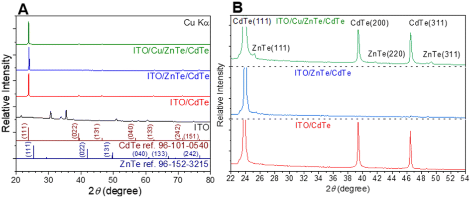 | ||
| Fig. 1 XRD patterns obtained from ITO/CdTe, ITO/ZnTe/CdTe, and ITO/Cu/ZnTe/CdTe, and from a bare ITO substrate (A and B). | ||
Top-view SEM images including the SEM-EDS analysis results of ITO/CdTe, ITO/ZnTe/CdTe, and ITO/Cu/ZnTe/CdTe are shown in Fig. 2A–C. The CdTe layer in ITO/CdTe was composed mainly of polyhedral faceted grains with sizes ranging from 500 nm to 2 μm as shown in Fig. 1A. As shown in Fig. 1B, the surface of ITO/ZnTe/CdTe exhibits larger and more homogeneous grains than those of ITO/CdTe. The increment in grain size can be attributed to the increase in the total film thickness as previously reported.11 In the case of ITO/Cu/ZnTe/CdTe, further increased grain sizes due to the decrease in the melting point by Cu addition were observed in the top-view SEM image shown in Fig. 1C.24 SEM-EDS analysis simultaneously performed with top-view observation shown in Fig. 1A–C reveals the composition ratio values of Te/(Zn + Cd) of around 1.2–1.3, indicating that all the prepared CdTe layers in ITO/CdTe, ITO/ZnTe/CdTe, and ITO/Cu/ZnTe/CdTe possess a Te rich composition. While Zn is not detected on ITO/ZnTe/CdTe, ITO/Cu/ZnTe/CdTe presents a homogeneous distribution of Zn detected as shown in Fig. 2F, with a Zn/(Cd + Zn) value of 0.2. The introduction of the Cu layer reduces the melting point of both ZnTe and CdTe as discussed above, resulting in an enhanced interdiffusion of Zn and Cd between the ZnTe and CdTe layers. In Fig. S19A,† XPS analysis revealed the presence of Cu species on the surface of ITO/Cu/ZnTe/CdTe, suggesting the segregation of Cu species to the surface during film deposition, and the segregation should enhance the decrease of the melting point.
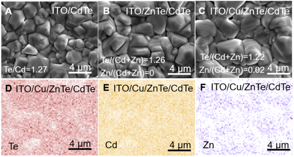 | ||
| Fig. 2 Plan-view SEM image (A–C) and SEM-EDS mapping results for ITO/Cu/ZnTe/CdTe (D–F). Composition ratios of Te/(Cd + Zn) and Zn/(Cd + Zn) obtained by simultaneously performed SEM-EDS analysis are expressed in the SEM images. | ||
To clarify the film structure of ITO/ZnTe/CdTe and ITO/Cu/ZnTe/CdTe, cross-sectional SEM-EDS analysis was conducted. High-resolution cross-sectional SEM images of backscattered electrons were obtained, as can be seen in Fig. 3A–D. The images were acquired with a focus on the CdTe and ZnTe layers separately to observe the microstructure differences. While no considerable variation can be pointed out on the CdTe layer in Fig. 3A and B, the ZnTe layer exhibits clear morphological alterations. In Fig. 3C, ITO/ZnTe/CdTe/CdS presents a high density of grain boundaries, with small grains present at the back contact interface. On the other hand, the introduction of the Cu layer produces changes, especially in the structure of the ZnTe layer in the ITO/Cu/ZnTe/CdTe specimen, as can be seen in Fig. 3D. The small grains observed at the ZnTe-ITO interface in ITO/ZnTe/CdTe disappeared, and the ZnTe layer was composed of pillar-shaped grains with significantly fewer clear grain boundaries between the ITO layer and photocathode surface than in the case without Cu addition. SEM-EDS line analysis results are shown in Fig. 3E–G. In the case of ITO/ZnTe/CdTe/CdS, there are clear plateau regions of the Zn/(Zn + Cd) ratio in ZnTe and CdTe layers but not in ITO/Cu/ZnTe/CdTe/CdS, and it can thus be concluded that the compositional gradient of the Zn/(Zn + Cd) ratio was introduced in ITO/Cu/ZnTe/CdTe/CdS via interdiffusion between ZnTe and CdTe as mentioned above. The cross-sectional SEM-EDS analysis results for ITO/Cu/ZnTe/CdTe with different ZnTe thicknesses shown in Fig. S14 in the ESI† show the formation of solid solution clearly because of the disappearance of the pure ZnTe layer. It should be noted that the composition gradient should be beneficial for charge separation, especially for photoexcited electrons, through forming a CBM gradient.
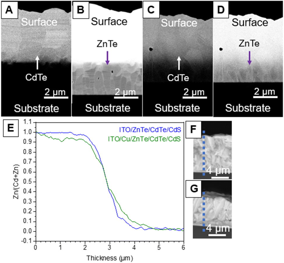 | ||
| Fig. 3 Cross-sectional SEM images focused on CdTe (A and C), and those focus on ZnTe (B and D), for ITO/ZnTe/CdTe/CdS and ITO/Cu/ZnTe/CdTe/CdS, respectively, SEM-EDS line analysis results (E), and cross-sectional SEM images with the dashed line indicating analysis performed lines for ITO/ZnTe/CdTe/CdS (F) and ITO/Cu/ZnTe/CdTe/CdS (G). | ||
Cross-sectional SEM-EBSD analyses were also conducted on ITO/ZnTe/CdTe and ITO/Cu/ZnTe/CdTe as shown in Fig. 4A and B, revealing substantial changes in the grain size and structure due to the Cu addition. In Fig. 4A, ITO/ZnTe/CdTe exhibits the presence of small grains, particularly in the ZnTe layer, and there are clear grain boundaries between the ZnTe and CdTe layers. This experimental fact indicates that the CdTe layer was not grown epitaxially on grains in the ZnTe layer. On the other hand, as shown in Fig. 4B, ITO/Cu/ZnTe/CdTe presented clearly larger grains than in the case without Cu addition, ITO/ZnTe/CdTe, and, surprisingly, there is no clear interface between ZnTe and CdTe layers, indicating epitaxial growth of the CdTe layer on ZnTe grains with the formation of the composition gradient. The analysis results reveal that the columnar grains observed in the cross-sectional SEM images shown in Fig. 3C and D are composed of ZnxCd1−xTe (0 ≤ x ≤ 1) with a composition gradient. This structure is advantageous for PEC hydrogen evolution because of the enhancement of charge separation by the CBM gradient and fewer grain boundaries, which can work as recombination centres and/or increase series resistance. SEM-EBSD also revealed the existence of crystal orientation 60-degree rotated domains in the apparent monograin observed for both ITO/ZnTe/CdTe and ITO/Cu/ZnTe/CdTe as shown in Fig. S1A–D in the ESI.† However, ITO/Cu/ZnTe/CdTe shows clearly fewer of the rotated domains than ITO/ZnTe/CdTe, and as such it can be interestingly concluded that the Cu addition effectively suppresses the formation of rotated domains.
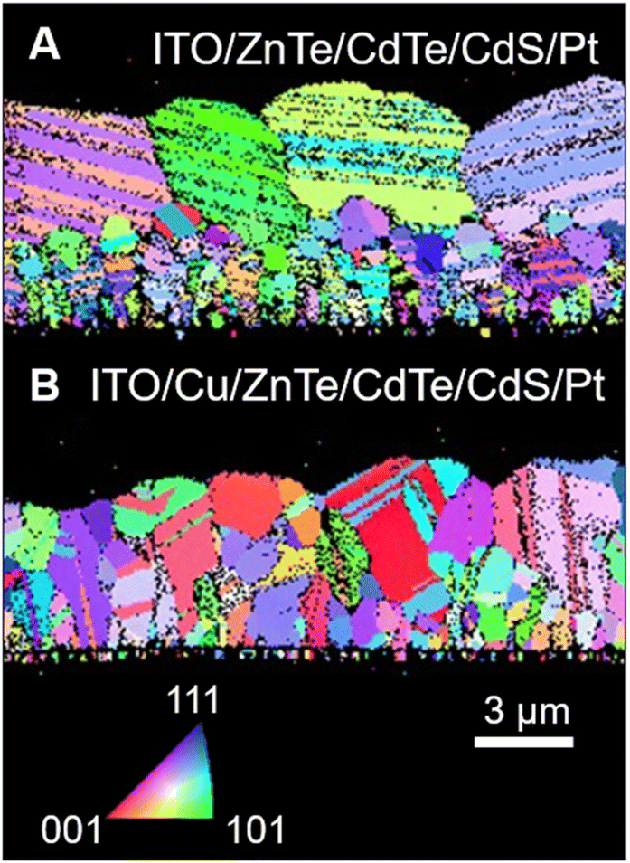 | ||
| Fig. 4 EBSD maps for ITO/ZnTe/CdTe/CdS/Pt (A) and ITO/Cu/ZnTe/CdTe/CdS/Pt (B). The EBSD maps are normal-direction inverse pole figures. | ||
To assess the optical absorption edge wavelength and band edge potentials, ultraviolet-visible diffuse reflectance spectroscopy (UV-Vis DRS) and PESA measurements were conducted. The UV-Vis DRS spectra shown in Fig. S2 in the ESI† revealed that ITO/CdTe, ITO/ZnTe/CdTe and ITO/Cu/ZnTe/CdTe showed almost the same absorption edge wavelength of about 840 nm. PESA spectra shown in Fig. S3 in the ESI† also determined VBM potentials of 5.28 eV for ITO/CdTe and 5.30 eV for ITO/ZnTe/CdTe, respectively. It should be noted that the PESA measurement is surface sensitive and thus the measurement refers to the surface of the specimen.
PEC properties of CdTe based photocathodes
Current–potential curves obtained from the ITO/CdTe surface modified with CdS and Pt (ITO/CdTe/CdS/Pt), the ITO/ZnTe/CdTe surface modified with CdS and Pt (ITO/ZnTe/CdTe/CdS/Pt), the ITO/Cu/ZnTe/CdTe surface modified with CdS and Pt (ITO/Cu/ZnTe/CdTe/CdS/Pt), and the RTA treated ITO/Cu/ZnTe/CdTe surface modified with CdS and Pt (ITO/Cu/ZnTe/CdTe/CdS/Pt (RTA)) photocathodes under simulated AM 1.5 G sunlight are presented in Fig. 5. ITO/CdTe/CdS/Pt showed a photocurrent of −7.7 mA cm−2 at 0 VRHE with an OP of 0.6 VRHE. However, the introduction of ZnTe in ITO/ZnTe/CdTe/CdS/Pt resulted in a severe reduction in photocurrent, dropping to less than 1/4, with a value of −1.5 mA cm−2 at 0 VRHE, while its OP was enhanced to 0.7 VRHE.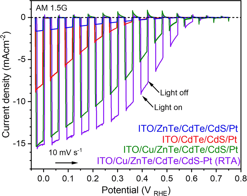 | ||
| Fig. 5 Current–potential curves for ITO/CdTe/CdS/Pt, ITO/ZnTe/CdTe/CdS/Pt, ITO/Cu/ZnTe/CdTe/CdS/Pt, and ITO/Cu/ZnTe/CdTe/CdS/Pt (RTA) under chopped simulated sunlight. 1 M aqueous KPi solution with pH adjusted to 6.5 was used as an electrolyte. The applied potential was swept at +10 mV s−1. | ||
Variations in CdTe and ZnTe thickness did not significantly affect the PEC performance, suggesting that the low cathodic photocurrent was caused by the high resistivity due to the larger number of grain boundaries, and the presence of small grains in the ZnTe layer. Attempts to improve thin-film quality by annealing with a CdCl2 coating over the electrode surface was performed following previously reported protocols.13,25 Nevertheless, 15 minutes of thermal treatment at 400 °C caused severe damage to the photocathode, leading to the film peeling off the substrate during the PEC measurement. As depicted in Fig. S4 in the ESI,† SEM-EDS analysis on the back side of the peeled-off film revealed a high concentration of Cd due to excessive migration from the CdTe layer, which may weaken the adhesion over the ITO. As cross-sectional SEM observations revealed, there are significant grain boundaries between CdTe and ZnTe layers, and small grains in the ZnTe layer. These structural features of ITO/ZnTe/CdTe resulted in large series resistance, which leads to a small photocurrent. To improve the PEC performance, the addition of Cu through a Cu layer deposition prior to the ZnTe and CdTe deposition was explored. ITO/Cu/CdTe/ZnTe/CdS/Pt showed a significantly enhanced photocurrent and OP of −14.6 mA cm−2 at 0 VRHE and >0.7 VRHE, respectively. This notable increase is the result of a series of factors, including improvements in the structural and electrical properties through Cu addition. It is known that Cu addition can decrease series resistance by increasing the hole concentration and make grains larger for both ZnTe and CdTe.26 Furthermore, the Cu addition resulted in the formation of a preferable film structure: grains with a pillar shape composed of a solid solution of ZnxCd1−xTe with a composition gradient as clarified by the cross-sectional SEM observations. The amount of Cu additive was optimized to be 1 nm, as summarized in Fig. S7 in the ESI.† The Mott–Schottky plots revealed the p-type behaviour expected for the ITO/Cu/ZnTe/CdTe specimen, with a flat band potential of around 0.8 VRHE as shown in Fig. S5 in the ESI.† The introduction of a multilayer structure and Cu addition clearly enhanced PEC hydrogen evolution from water. However, there is still room to increase the photocurrent considering the expected photocurrent of 29 mA cm−2 from the absorption edge wavelength of CdTe. To further facilitate PEC hydrogen evolution, post-deposition annealing treatment by the RTA technique on ITO/Cu/ZnTe/CdTe was studied. It should be noted that the post-deposition RTA treatment is reported to improve the performance of CdTe-based photovoltaic devices with Cu added to the ZnTe back contact, through passivating recombination sites accompanied by the segregation of Cu, and this effect should also work on the CdTe-based photocathode.27 RTA treatment for one minute at 400 °C on ITO/Cu/ZnTe/CdTe resulted in a significant increase in photocurrent at >0 VRHE; ITO/Cu/ZnTe/CdTe/CdS/Pt (RTA) showed a significantly increased photocurrent at 0.5 VRHE from −1.7 to −4.0 mA cm−2 over ITO/Cu/ZnTe/CdTe/CdS/Pt. RTA treatment for longer than a minute and at higher than 400 °C resulted in the film peeling away from the ITO coated glass plate. To assess the effects of the RTA treatment, the series resistance (Rs) and parallel resistance (Rp) were obtained from a gradient of current–potential curves between 0 VRHE and 0.05 VRHE, and 0.4 VRHE and 0.47 VRHE, respectively, resulting in 21 Ω and 106 Ω for ITO/Cu/ZnTe/CdTe/CdS/Pt (RTA), and 26 Ω and 52 Ω for ITO/Cu/ZnTe/CdTe/CdS/Pt.
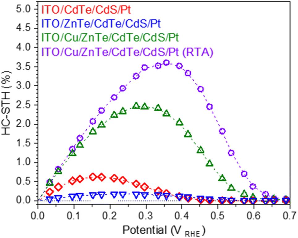
The slightly decreased Rsvia RTA treatment may be caused by the improved electric contact between the ZnTe layer and ITO layer. The significantly increased Rp is likely caused by increased resistivity, which contributes to enhanced charge separation through increasing depletion layer thickness. Mott–Schottky plots also confirm the Rp increase through RTA treatment; the acceptor concentration of ITO/Cu/ZnTe/CdTe was decreased from 4 × 1017 cm−3 to 2 × 1017 cm−3 post RTA treatment. It should be noted that the plots refer to acceptor concentration in the depletion layer region, and this decrease of acceptor concentration is likely caused by the segregation of excessive Cu around the surface of the CdTe layer. On the other hand, the slight decrease of Rs by RTA treatment is also due to the segregation of Cu species at the ITO-ZnTe interface as reported.20,27 Comparing the reported photocathodes so far, the novel ITO/Cu/ZnTe/CdTe/CdS/Pt (RTA) photocathode shows higher OP and photocurrent values at around an OP of 0.7 VRHE, and −4.0 mA cm−2 at 0.5 VRHE than reported by Su et al., at 0.6 VRHE, and −2.4 mA cm−2 at 0.5 VRHE.13 The enhancement of PEC hydrogen evolution at relatively high potential, around OP, is due to enhanced charge separation by the composition gradient, pillar shaped grains, and well-controlled electrical properties. The HC-STH curve obtained from the current potential curves is shown in Fig. 6. The maximum HC-STH for ITO/CdTe/CdS/Pt, ITO/Cu/ZnTe/CdTe/CdS/Pt, and ITO/Cu/ZnTe/CdTe/CdS/Pt (RTA) was 0.6% at 0.15 VRHE, 2.5% at 0.27 VRHE and 3.6% at 0.36 VRHE, respectively. ITO/Cu/ZnTe/CdTe/CdS/Pt (RTA) showed 6 times higher HC-STH than ITO/CdTe/CdS/Pt. It should be noted that the highest HC-STH value of 3.6% at 0.36 VRHE among the examined photocathodes is comparable to the highest HC-STH value of reported CdTe based photocathodes, 3.7% at 0.3 VRHE.13
 | ||
| Fig. 6 HC-STH curves calculated from the current–potential curves for ITO/CdTe/CdS/Pt, ITO/ZnTe/CdTe/CdS/Pt, ITO/Cu/ZnTe/CdTe/CdS/Pt, and ITO/Cu/ZnTe/CdTe/CdS/Pt (RTA) shown in Fig. 5. | ||
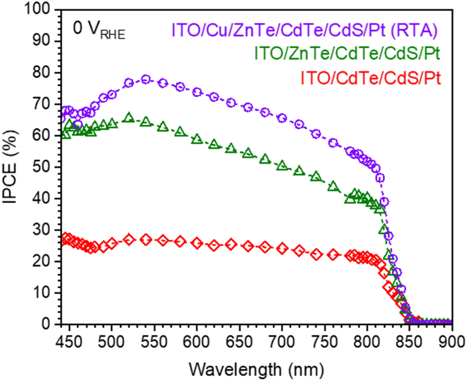
The IPCE of these photocathodes determined under monochromatic light at 0 VRHE is plotted in Fig. 7. ITO/Cu/ZnTe/CdTe/CdS/Pt and ITO/Cu/ZnTe/CdTe/CdS/Pt (RTA) photocathodes exhibited clearly higher IPCEs across the whole spectrum in comparison to ITO/CdTe/CdS/Pt. The IPCE value decrease with the light wavelength on these photocathodes below 540 nm is caused by the existence of a surface modifier, CdS layer. The light absorbed by the CdS layer did not contribute to the PEC reaction because of its low crystallinity, favouring the photoexcited carrier recombination.11,21 Interestingly, ITO/Cu/ZnTe/CdTe/CdS/Pt (RTA) exhibits an IPCE spectrum with >70% in a wide range, from 480 to 640 nm, and a maximum value of 78% at 540 nm. The expected photocurrent under AM 1.5G light based on these IPCE values is 15.9 mA cm−2 for ITO/Cu/ZnTe/CdTe/CdS/Pt (RTA) and is very consistent with the current–potential curve shown in Fig. 5.
 | ||
| Fig. 7 IPCE spectra obtained from ITO/CdTe/CdS/Pt, ITO/ZnTe/CdTe/CdS/Pt and ITO/Cu/ZnTe/CdTe/CdS/Pt photocathodes at 0 VRHE under monochromatic light. As an electrolyte, a 1 M aqueous KPi solution with pH adjusted to 6.5 was employed. | ||
To aid the understanding of the enhanced photocurrent enhancement and OP, schematic band diagrams at the solid–liquid interface for the bilayer structure and composition gradient are presented in Fig. 8A and B. The introduction of the composition gradient leads to the formation of a gradient in the CBM. In the bilayer structure, photogenerated carriers can mainly be used inside the depletion layer. However, the potential gradient allows the harnessing of electrons outside the depletion layer.17 In addition, the VBM of CdTe and ZnTe permits hole-selective diffusion to the back side electrode, ITO. These band alignment features could explain the enhanced hydrogen evolution from water at high potential in the case of the TO/Cu/ZnTe/CdTe/CdS/Pt (RTA) photocathode.
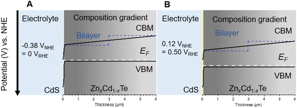 | ||
| Fig. 8 Expected band diagrams for the cases of the bilayer structure and the composition gradient structure of ZnTe and CdTe at (A) 0 VRHE and (B) 0.5 VRHE. | ||
Durability and faradaic efficiency of the ITO/Cu/CdTe/CdS/Pt (RTA) photocathode
The time course of the photocurrent generated by the ITO/Cu/ZnTe/CdTe/CdS/Pt (RTA) photocathode at 0 VRHE is presented in Fig. 9. Following irradiation, the photocurrent generated was −13.3 mA cm−2, which slightly increased to −15.0 mA cm−2 during the first 20 minutes. Subsequently, after 2 hours, the photocurrent decreased to −13.6 mA cm−2. The decrease continued until stabilising at −11 mA cm−2 without suffering any significant fluctuation for about 21 hours. After about 13 hours, stirring was interrupted intentionally for a minute. However, the interruption did not decrease the photocurrent significantly, less than 1 mA cm−2, indicating that the mass transport is not significant in this case. After 21 hours, the irradiation and stirring were intentionally interrupted, and, as a result, the photocurrent increased to −14 mA cm−2 followed by a steady decrease over a couple of hours, to −12 mA cm−2. This recoverable decrease of cathodic photocurrent can be cause by the temporal poisoning with Cd.28 The standard electrode potential of Cd is −0.403 V vs. the standard hydrogen electrode (SHE), −0.02 VRHE at pH 6.5, and, thus, Cd species in an electrolyte originating from corrosion of CdS and CdTe can be reduced to be metallic Cd and deposit on the photocathode surface under PEC hydrogen evolution conditions while the deposited metallic Cd can be oxidized and removed at 0 VRHE under dark conditions.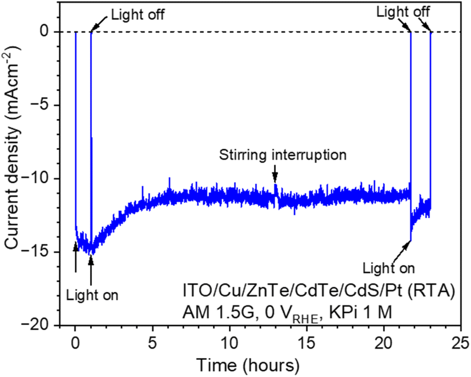 | ||
| Fig. 9 Time course of the photocurrent generated by an ITO/Cu/ZnTe/CdTe/CdS/Pt photocathode at 0 VRHE under simulated sunlight in 1 M KPi aqueous solution under 400 rpm stirring. | ||
In Fig. S6 in the ESI,† plan-view SEM images and XPS analysis results obtained for the samples before and after the stability test are shown. The surface photocathode does not present apparent morphology changes. However, the XPS peak intensity of S slightly decreased after 23 hours of irradiation as shown in Fig. S6D in the ESI,† suggesting a possible corrosion of the CdS layer.29
To confirm the faradaic efficiency of the ITO/Cu/ZnTe/CdTe/CdS/Pt (RTA) photocathode, the evolved amount of hydrogen and oxygen under irradiation with an applied potential of 0 VRHE was measured using a microGC. As shown in Fig. 10, it was confirmed that the faradaic efficiency for hydrogen and oxygen evolution was almost 100%. Moreover, the evolution ratio between hydrogen and oxygen was stoichiometric, 2![[thin space (1/6-em)]](https://www.rsc.org/images/entities/char_2009.gif) :1, indicating that the photocurrent observed in PEC measurements contributes to the water-splitting reaction. It should be noted that because of the limited geometric photocathode surface area of 0.11 cm−2 with a planar shape, the back reaction was negligible.
:1, indicating that the photocurrent observed in PEC measurements contributes to the water-splitting reaction. It should be noted that because of the limited geometric photocathode surface area of 0.11 cm−2 with a planar shape, the back reaction was negligible.
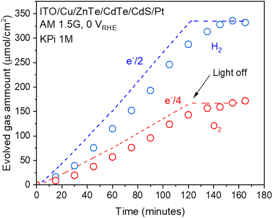 | ||
| Fig. 10 Hydrogen and oxygen evolution from the ITO/Cu/ZnTe/CdTe/CdS/Pt (RTA) photocathode under simulated sunlight in a three-electrode configuration with an applied potential of 0 VRHE. The expected amounts of hydrogen and oxygen (denoted as e−/2 and e−/4, respectively) as calculated from the observed photocurrent are shown as dashed lines. A 1 M aqueous KPi solution with pH adjusted to 6.5 with KOH was used as the electrolyte. | ||
Conclusions
In this study, the PEC properties of bilayer photocathodes of ZnTe and CdTe with the formation of a composition gradient prepared by CSS were investigated. The introduction of a ZnTe layer between the ITO back contact and CdTe layer resulted in a severe decrease in photocurrent due to the small grain size of the ZnTe layer and significant boundaries between the ZnTe and CdTe layers. The Cu addition significantly enhanced PEC hydrogen evolution through the variation of the electrical and structural properties of ZnTe and CdTe layers: an increase in the hole concentration, an increase of the grain size, and the formation of columnar grains composed of ZnTe and CdTe with a composition gradient through the formation of ZnxCd1−xTe by interdiffusion. These structural changes were responsible for a tenfold enhancement of the photocurrent to −14.9 mA cm−2 and OP > 0.7 VRHE. The simulated band diagram showed the formation of a gradient in the CBM because of the composition gradient, and the CBM gradient enhanced the charge separation, especially outside the depletion layer formed at the solid–liquid interface. Post-deposition RTA treatment significantly increased Rp and slightly decreased Rs through the segregation of the Cu additive and resulted in an increase in photocurrent at higher potentials to −4.0 mA cm−2 at 0.7 VRHE, the highest value among CdTe-based photocathodes, achieving a STH of 3.6% at 0.36 VRHE. IPCEs revealed that the examined CdTe based photocathodes respond to light with wavelengths shorter than about 850 nm. ITO/Cu/ZnTe/CdTe/CdS/Pt (RTA) showed an IPCE spectrum with >70% in a wide range, from 480 to 640 nm, a maximum value of 78% at 540 nm, and a durable photocurrent of −11.0 mA cm−2 for longer than 23 hours. It can be concluded that ITO/Cu/ZnTe/CdTe/CdS/Pt (RTA) is one of the most efficient photocathodes for the hydrogen evolution reaction, with productivity and durability. Future challenges include further improvement of the photocurrent at higher potential by improving the surface modification, which may enhance the charge separation at the interface.Conflicts of interest
There are no conflicts to declare.Acknowledgements
This work was supported by Grants-in-Aid for Scientific Research (A) (No. 21H04551) from the Japan Society for the Promotion of Science (JSPS). A part of this work was supported by the “Advanced Research Infrastructure for Materials and Nanotechnology in Japan (ARIM)” of the Ministry of Education, Culture, Sports, Science and Technology (MEXT) (grant no. JPMXP1222UT0248 and JPMXP1223UT0039). The authors wish to thank M. Asami for the assistance with the analysis of the parallel and series resistance, and M. Nakabayashi for the assitance with the structural analysis using SEM-EDS and SEM-EBSD.References
- R. Metkemeijer and P. Achard, J. Power Sources, 1994, 49, 271–282 CrossRef CAS.
- J. A. Turner, Science, 2004, 305, 972–974 CrossRef CAS PubMed.
- N. S. Lewis and D. G. Nocera, Proc. Natl. Acad. Sci. U. S. A., 2006, 103, 15729–15735 CrossRef CAS PubMed.
- K. Maeda and K. Domen, J. Phys. Chem. Lett., 2010, 1, 2655–2661 CrossRef CAS.
- A. Kudo and Y. Miseki, Chem. Soc. Rev., 2009, 38, 253–278 RSC.
- J. H. Kim, D. Hansora, P. Sharma, J. W. Jang and J. S. Lee, Chem. Soc. Rev., 2019, 48, 1908–1971 RSC.
- T. Yao, X. An, H. Han, J. Q. Chen and C. Li, Adv. Energy Mater., 2018, 8, 1–36 Search PubMed.
- J. M. Burst, J. N. Duenow, D. S. Albin, E. Colegrove, M. O. Reese, J. A. Aguiar, C. S. Jiang, M. K. Patel, M. M. Al-Jassim, D. Kuciauskas, S. Swain, T. Ablekim, K. G. Lynn and W. K. Metzger, Nat. Energy, 2016, 1, 16015 CrossRef CAS.
- M. A. Scarpulla, B. McCandless, A. B. Phillips, Y. Yan, M. J. Heben, C. Wolden, G. Xiong, W. K. Metzger, D. Mao, D. Krasikov, I. Sankin, S. Grover, A. Munshi, W. Sampath, J. R. Sites, A. Bothwell, D. Albin, M. O. Reese, A. Romeo, M. Nardone, R. Klie, J. M. Walls, T. Fiducia, A. Abbas and S. M. Hayes, Sol. Energy Mater. Sol. Cells, 2023, 255, 112289 CrossRef CAS.
- K. Ohashi, J. Mccann and J. O. Bockris, Nature, 1977, 266, 610–611 CrossRef CAS.
- J. Su, T. Minegishi, M. Katayama and K. Domen, J. Mater. Chem. A, 2017, 5, 4486–4492 RSC.
- J. X. Jian, L. H. Xie, A. Mumtaz, T. Baines, J. D. Major, Q. X. Tong and J. Sun, ACS Appl. Mater. Interfaces, 2023, 15, 21057–21065 CrossRef CAS PubMed.
- J. Su, T. Minegishi and K. Domen, J. Mater. Chem. A, 2017, 5, 13154–13160 RSC.
- T. Higashi, H. Kaneko, T. Minegishi, H. Kobayashi, M. Zhong, Y. Kuang, T. Hisatomi, M. Katayama, T. Takata, H. Nishiyama, T. Yamada and K. Domen, Chem. Commun., 2017, 53, 11674–11677 RSC.
- L. Pan, J. H. Kim, M. T. Mayer, M. K. Son, A. Ummadisingu, J. S. Lee, A. Hagfeldt, J. Luo and M. Grätzel, Nat. Catal., 2018, 1, 412–420 CrossRef CAS.
- H. Kaneko, T. Minegishi, M. Nakabayashi, N. Shibata, Y. Kuang, T. Yamada and K. Domen, Adv. Funct. Mater., 2016, 26, 4570–4577 CrossRef CAS.
- T. Minegishi, S. Yamaguchi and M. Sugiyama, Appl. Phys. Lett., 2021, 119, 123905 CrossRef CAS.
- B. Chen, J. Liu, Z. Cai, A. Xu, X. Liu, Z. Rong, D. Qin, W. Xu, L. Hou and Q. Liang, Nanomaterials, 2019, 9, 626 CrossRef CAS PubMed.
- R. S. Hall, D. Lamb and S. J. C. Irvine, Energy Sci. Eng., 2021, 9, 606–632 CrossRef CAS.
- K. Shen, X. Wang, Y. Zhang, H. Zhu, Z. Chen, C. Huang and Y. Mai, Sol. Energy, 2020, 201, 55–62 CrossRef CAS.
- T. Minegishi, A. Ohnishi, Y. Pihosh, K. Hatagami, T. Higashi, M. Katayama, K. Domen and M. Sugiyama, APL Mater., 2020, 8, 041101 CrossRef CAS.
- K. Bashir, N. Mehboob, A. Ali, A. Zaman, M. Ashraf, M. Lal, K. Althubeiti and M. Mushtaq, Mater. Lett., 2021, 304, 130737 CrossRef CAS.
- J. Moseley, W. K. Metzger, H. R. Moutinho, N. Paudel, H. L. Guthrey, Y. Yan, R. K. Ahrenkiel and M. M. Al-Jassim, J. Appl. Phys., 2018, 118, 025702 CrossRef.
- C. R. Corwine, A. O. Pudov, M. Gloeckler, S. H. Demtsu and J. R. Sites, Sol. Energy Mater. Sol. Cells, 2004, 82, 481–489 CAS.
- N. Amin, M. R. Karim and Z. A. ALOthman, Crystals, 2021, 11, 1–16 Search PubMed.
- T. D. Dzhafarov, S. S. Yesilkaya, N. Y. Canli and M. Caliskan, Sol. Energy Mater. Sol. Cells, 2005, 85, 371–383 CrossRef CAS.
- C. A. Wolden, A. Abbas, J. Li, D. R. Diercks, D. M. Meysing, T. R. Ohno, J. D. Beach, T. M. Barnes and J. M. Walls, Sol. Energy Mater. Sol. Cells, 2016, 147, 203–210 CrossRef CAS.
- H. Kaneko, T. Minegishi, H. Kobayashi, Y. Kuang and K. Domen, J. Chem. Phys., 2019, 150, 041713 CrossRef PubMed.
- H. Kumagai, T. Minegishi, N. Sato, T. Yamada, J. Kubota and K. Domen, J. Mater. Chem. A, 2015, 3, 8300–8307 RSC.
Footnote |
| † Electronic supplementary information (ESI) available: SEM images, XRD patterns, UV-vis DRS spectra, PESA spectrum, EBSD maps, Mott–Schottky plots, optimized sample preparation conditions, and results of analysis of photoelectrochemical reaction products. See DOI: https://doi.org/10.1039/ |
| This journal is © The Royal Society of Chemistry 2024 |