DOI:
10.1039/D3NR04712A
(Paper)
Nanoscale, 2024,
16, 1331-1344
Magnetic-ferroelectric synergic control of multilevel conducting states in van der Waals multiferroic tunnel junctions towards in-memory computing†
Received
19th September 2023
, Accepted 2nd December 2023
First published on 5th December 2023
Abstract
van der Waals (vdW) multiferroic tunnel junctions (MFTJs) based on two-dimensional materials have gained significant interest due to their potential applications in next-generation data storage and in-memory computing devices. In this study, we construct vdW MFTJs by employing monolayer Mn2Se3 as the spin-filter tunnel barrier, TiTe2 as the electrodes and In2S3 as the tunnel barrier to investigate the spin transport properties based on first-principles quantum transport calculations. It is highlighted that apparent tunneling magnetoresistance (TMR) and tunneling electroresistance (TER) effects with a maximum TMR ratio of 6237% and TER ratio of 1771% can be realized by using bilayer In2S3 as the tunnel barrier under finite bias. Furthermore, the physical origin of the distinguished TMR and TER effects is unraveled from the k||-resolved transmission spectra and spin-dependent projected local density of states analysis. Interestingly, four distinguishable conductance states reveal the implementation of four-state nonvolatile data storage using one MFTJ unit. More importantly, in-memory logic computing and multilevel data storage can be achieved at the same time by magnetic switching and electrical control, respectively. These results shed light on vdW MFTJs in the applications of in-memory computing as well as multilevel data storage devices.
 Baisheng Sa | Baisheng Sa received his B.Sc. degree (2008) in Materials Science and Engineering and Ph.D. (2014) in Materials Physics and Chemistry from Xiamen University. He is currently a professor in the School of Materials Science and Engineering at Fuzhou University. His research interests are integrated computational modelling, density functional theory calculations and machine learning design of novel low-dimensional materials and van der Waals heterostructures for energy, environment and electronic materials. He was recognized as one of the top 1% of highly cited authors in Royal Society of Chemistry journals (2019) and awarded by the Outstanding Young Scientists Foundation of Fujian Province of China (2021). |
Introduction
Nowadays, the integration of big data storage and artificial intelligence technologies, which offer significant opportunities across various industries, and deliver more efficient, intelligent, and personalized services and products, is driving comprehensive societal transformation.1–4 The emergence of these technologies requires electronic devices having faster data writing speeds, smaller data storage footprints, and lower energy consumption.5,6 Among various information-integrated storage devices, multiferroic tunnel junctions (MFTJs), combining the electrical behaviors of magnetic tunnel junctions (MTJs) and ferroelectric tunnel junctions (FTJs), have become extremely promising approaches to meet the requirements of low power, high density, non-volatile memory and versatile logic devices.7,8 Herein, MTJs are composed of two ferromagnetic electrodes and an intermediate tunnel barrier layer (such as MgO, GaAs, etc.).9–12 The spin-dependent tunneling current of the MTJ depends on the relative orientation (parallel or antiparallel) of the magnetization of two ferromagnetic electrodes, resulting in the tunneling magnetoresistance (TMR) effect.13,14 On the other hand, FTJ consists of a thin ferroelectric barrier layer sandwiched by two metallic electrodes. The polarization dependent tunneling current of the FTJ depends on the ferroelectric polarization direction of the potential barrier, resulting in the tunneling electroresistance (TER) effect.15–17
MFTJs can be obtained by replacing the dielectric barrier of MTJs with a ferroelectric tunneling barrier, or by substituting the metal electrodes of FTJs with ferromagnetic materials.18 The resistances of MFTJs can switch between different nonvolatile states under external electric or magnetic fields, which provides a new way to realize high-density data storage or in-memory computing.19,20 The possibility of TMR conversion in MTJs with ferroelectric barriers and the coexistence of TMR and TER effects in MFTJs21 spark significant attention towards MFTJs as rising star candidates for next generation information storage applications.22–24 In the early years, three-dimensional (3D) ferromagnetic metals were utilized as the ferromagnetic electrode, where the sign of TMR could be reversed by switching the ferroelectric polarization direction in some 3D ferromagnetic metal based MFTJs, such as La0.7Sr0.3MnO3/PbZr0.2Ti0.8O3/Co and La0.7Sr0.3MnO3/BaTiO3/NiFe MFTJs.25,26 However, 3D ferromagnetic metals usually have low spin polarizations, which lead to limited TMR values in 3D ferromagnetic metal-based MFTJs.27 Through replacing the ferromagnetic metallic electrodes of MFTJs with half-metallic perovskites, considerable TMR effects can be realized.28,29 For instance, the La0.7Sr0.3MnO3/SrTiO3/BaTiO3/La0.7Sr0.3Mn0.8Ru0.2O3 MFTJ can realize a TMR of 30% and a TER of ∼128%.30 It is reported that a TMR of 300% and a TER of 160% can be observed in the La0.7Ca0.3MnO3/Ba0.5Sr0.5TiO3/La0.7Ca0.3MnO3 MFTJ.20 Nevertheless, some persisting troubles, such as the critical ferroelectric film thickness, defective inhomogeneous interfaces and high resistance-area (RA) products, still limit the application of 3D MFTJs.19,31,32
With the emergence of graphene and other two-dimensional (2D) materials, 2D van der Waals (vdW) materials come into the view of researchers.33–35 2D vdW materials possess an atomic thin thickness and perfect interface without dangling bonds, which can overcome the tricky troubles in 3D MFTJs.36,37 For example, FemGeTe2/In2Se3/FenGeTe2 (m, n = 3, 4, 5; m ≠ n) vdW MFTJs are predicted to possess a remarkably low RA product of less than 1 Ω μm2, which makes such vdW MFTJs superior to conventional MFTJs for nonvolatile memory applications.38 Lately, a much lower RA product (less than 0.1 Ω μm2) was revealed in a CrSe2/CuInP2S6/CrSe2 MFTJ.39 However, the TMR and TER ratios in these 2D MFTJs are still restricted to a relatively low level, which is not conducive to their practical application. On the other hand, most 2D magnetic materials possess a low Curie temperature, which could be another crucial reason limiting the application of these 2D MFTJs.40 Recently, ferromagnetic Mn2Se3 monolayers were demonstrated to possess a high Curie temperature of 820 K, and their intrinsic half-metallicity implies that a good performance could be achieved in spintronic devices.41 Therefore, the potential applications of ferromagnetic Mn2Se3 monolayers in vdW MFTJs are anticipated and a corresponding systematic investigation is of great interest and importance. It is interesting to note that giant TER effects have been realized in In2X3 (X = S, Se, Te) monolayers and bilayers,42,43 and the In2Se3/graphene lateral FTJs and Fe3GeTe2/binary In2Se3/Fe3GeTe2 MFTJs have been reported to exert excellent TER and TMR effects.44,45 Herein, the 2D lattice of In2S3 matches the Mn2Se3 monolayer very well.41,46,47 Hence, the construction of vdW MFTJs by combining In2S3 and Mn2Se3 together is possible.
In this work, we investigated the spin transport properties of MFTJs by employing monolayer Mn2Se3 as the spin-filter tunnel barrier and monolayer or bilayer In2S3 as the tunnel barrier. The results reveal that the MFTJs with monolayer In2S3 as the tunnel barrier only can realize the apparent TMR effect, while the TER effect is hard to achieve. Interestingly, both apparent TMR and TER effects can be achieved in the MFTJs with bilayer In2S3 as the tunnel barrier. Moreover, the MFTJ exhibits four distinct conductance states, indicating the possibility of achieving four-state data storage. By arranging numerous MFTJs into an N × N array, integrated storage and computing functionalities can be feasibly realized.
Computational details
The structures of 2D monolayers and heterostructures were built by using the ALKEMIE platform,48,49 and the calculations were implemented in Vienna ab initio simulation package (VASP) based on density functional theory (DFT).50,51 The Perdew–Burke–Ernzerhof (PBE) functional of generalized-gradient approximation (GGA) was employed to deal with the exchange–correlation potential.52 The interlayer van der Waals (vdW) interactions between 2D materials were considered with the DFT-D3 method.53 The effective on-site coulombic interaction was set to 3 eV for Mn atoms, which can well reproduce the results by using the accurate HSE06 functional.41 The plane wave energy cutoff was set to 500 eV, and the k-point sampling grid was set to 15 × 15 × 1 for the structure optimization and self-consistent calculations. A vacuum space of 20 Å was inserted along the z-direction to avoid the interaction of adjacent layers. The energy convergence criterion was set as 1 × 10⁻⁶ eV, and the atomic positions were relaxed until the force of each atom was less than 0.01 eV Å−1. The dipole correction was taken into consideration to avoid the effect of the vacuum electric field.54
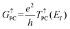
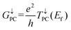
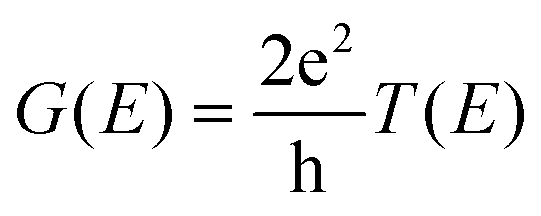
The optimization and transmission properties of the devices were carried out using the non-equilibrium Green's function (NEGF) method as implemented in the QuantumWise Atomistix ToolKit (QuantumATK) package.55,56 The GGA-PBE functional with a linear combination of atomic orbital (LCAO) norm-conserving PseudoDojo pseudopotential57 was employed to account for the electron exchange and correctional interactions. The valence electrons were expanded in a numerical atomic-orbital basis set of double-zeta polarization (DZP) for all atoms.58 The effective on-site coulombic interaction was set to 3 eV for Mn atoms as well. The cutoff energy was set to 105 Hartree, and the Monkhorst–Pack k-point meshes for the central scattering regions and electrodes were set to 10 × 10 × 1 and 10 × 10 × 150. To ensure the accuracy of the results, a 121 × 121 k-point mesh was employed in the spin-dependent transmission calculations. The convergence criterion of the force was set to 0.01 eV Å−1. The relationship between spin-dependent conductance and transmission of the tunnel junction per unit cell area can be described by the Landauer Büttiker formula:59,60
| |  | (1) |
where

is the
k-point averaged transmission function at energy
E and
T(
k||,
E) is the
k resolved transmission function with
k|| = (
kx,
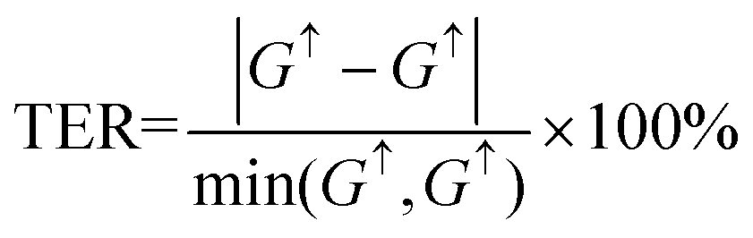
ky). The tunnel electroresistance (TER) ratio is calculated through the formula
61| |  | (2) |
where
G↑ and
G↓ are the tunneling conductances of the FTJs when the In
2S
3 ferroelectric layer is in the up-polarized and down-polarized states, respectively. The tunnel magnetoresistance (TMR) ratio is calculated by using the formula
14| | | TMR = (GPC − GAPC)/GAPC × 100% | (3) |
where
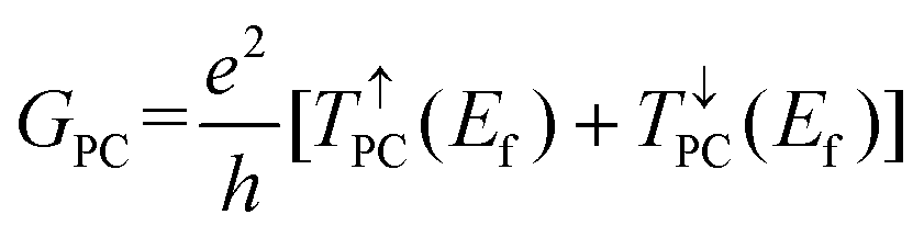
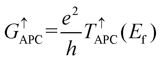
GPC and
GAPC are the total spin-dependent conductance of PC and APC states, which are defined as
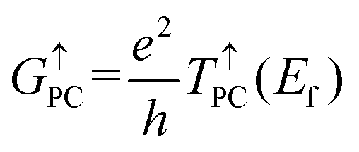
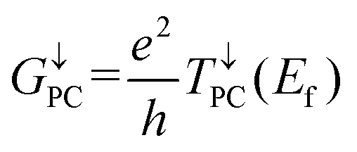
| |  | (4) |
| |  | (5) |
where
e and
h are the electron charge and Planck's constant, respectively,
T↑PC(
Ef) and
T↓PC(
Ef) represent the spin-up and spin-down transmission coefficients at the Fermi level when the vdW MTJs are in the PC state, and
T↑APC(
Ef) and
T↓APC(
Ef) represent the spin-up and spin-down transmission coefficients at the Fermi level when the vdW MTJs are in the APC state. The resistance-area (RA) products are calculated from the transmission at the Fermi level from
| |  | (6) |
where
S is the unit cell area and
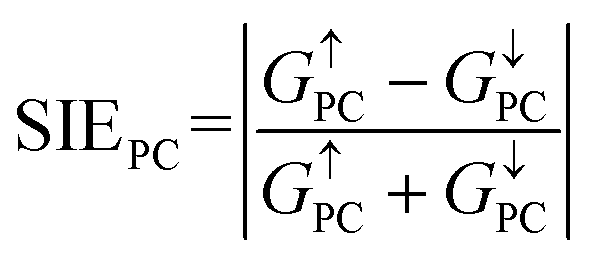
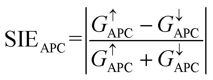
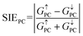
G is the total conductance. The spin injection efficiency (SIE) is defined as
| |  | (7) |
| | 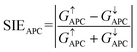 | (8) |
where
G↑PC and
G↓PC are the conductances of spin-up and spin-down channels when the vdW MTJs are in the PC state, respectively,
G↑APC and
G↓APC are the conductances of spin-up and spin-down channels when the vdW MTJs are in the APC state, respectively, and they can be calculated by using
| |  | (9) |
| |  | (10) |
| |  | (11) |
| |  | (12) |
Results and discussion
To construct the In2S3 and Mn2Se3 based MFTJs, we screened potential electrode materials from the ALKEMIE materials database according to the following four criteria: layered crystal structure, well matching lattice parameters, binary chalcogenide, and metallic electronic structure nature. Firstly, with a layered crystal structure, the different parts of the proposed MFTJs can be constructed by vertical assembling. Secondly, the well matching lattice parameters indicate the potential of epitaxial growth for different materials. Thirdly, the binary compound ensures the simplicity of the electrode materials, and the vdW interactions between chalcogen layers increase the possibility to obtain vdW MFTJs. Lastly, the metallic electronic structure nature guarantees the good electrical conductivity of the electrode. As the screening result, TiTe2 with a metallic band structure and suitable hexagonal vdW layered crystal structure is proposed as the suitable electrode material.62–65
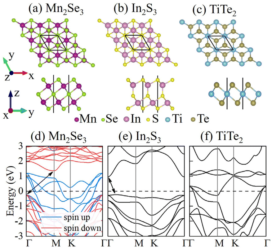
The geometric structures of Mn2Se3, In2S3 and TiTe2 monolayers with the P![[3 with combining macron]](https://www.rsc.org/images/entities/char_0033_0304.gif) m1 space group are shown in Fig. 1. From the side view of these structures, the Mn2Se3 and In2S3 monolayers are formed by alternately stacking two Mn/In and three Se atomic layers. From the top view of Mn2Se3 structures in Fig. 1(a), the upper Se and Mn atoms directly face the bottom Mn and Se atoms, respectively. From the top view of In2Se3 structures in Fig. 1(b), the upper S atoms directly face the bottom S atoms, and the middle S atoms directly face the upper In atoms. It is worth noting that the middle S atoms can move to directly face the bottom In atoms when applying an appropriate external electric field, making In2S3 a typical ferroelectric material.47,66 From the top view of TiTe2 structures in Fig. 1(c), a TiTe2 monolayer shows a Te–Ti–Te sandwich layer, which is similar to the metallic 1T-phase MoS2. Herein, the optimized lattice constants a are 3.708, 3.909 and 3.722 Å for Mn2Se3, In2S3 and TiTe2 monolayers, consistent with previous works.41,64,67 The maximum lattice mismatch is about 5%, within a reasonable range. Besides, the optimized lattice constants for bulk TiTe2 are a = 3.744 Å, c = 6.478 Å, which are very close to the experimental values (a0 = 3.777 Å, c0 = 6.498 Å),68 verifying the reliability of our calculations. As depicted in Fig. 1(d), (e) and (f), the calculated electronic band structures of Mn2Se3, In2S3 and TiTe2 monolayers show ferromagnetic half-metallic, semiconducting and metallic behaviors, respectively. The band structure of bulk TiTe2 in Fig. S1† also represents the typical metallic behavior, demonstrating that both the monolayer and bulk structures of TiTe2 can be competent as electrode materials. Since the emergence of a (2 × 2) charge density wave (CDW) order has been realized only in single-layer TiTe2, while no CDW transitions is observed in two-layer and multi-layer TiTe2.65 In this work, multi-layer TiTe2 is regarded as the electrode of MFTJs. The CDW transformation of TiTe2 is not taken into account.
m1 space group are shown in Fig. 1. From the side view of these structures, the Mn2Se3 and In2S3 monolayers are formed by alternately stacking two Mn/In and three Se atomic layers. From the top view of Mn2Se3 structures in Fig. 1(a), the upper Se and Mn atoms directly face the bottom Mn and Se atoms, respectively. From the top view of In2Se3 structures in Fig. 1(b), the upper S atoms directly face the bottom S atoms, and the middle S atoms directly face the upper In atoms. It is worth noting that the middle S atoms can move to directly face the bottom In atoms when applying an appropriate external electric field, making In2S3 a typical ferroelectric material.47,66 From the top view of TiTe2 structures in Fig. 1(c), a TiTe2 monolayer shows a Te–Ti–Te sandwich layer, which is similar to the metallic 1T-phase MoS2. Herein, the optimized lattice constants a are 3.708, 3.909 and 3.722 Å for Mn2Se3, In2S3 and TiTe2 monolayers, consistent with previous works.41,64,67 The maximum lattice mismatch is about 5%, within a reasonable range. Besides, the optimized lattice constants for bulk TiTe2 are a = 3.744 Å, c = 6.478 Å, which are very close to the experimental values (a0 = 3.777 Å, c0 = 6.498 Å),68 verifying the reliability of our calculations. As depicted in Fig. 1(d), (e) and (f), the calculated electronic band structures of Mn2Se3, In2S3 and TiTe2 monolayers show ferromagnetic half-metallic, semiconducting and metallic behaviors, respectively. The band structure of bulk TiTe2 in Fig. S1† also represents the typical metallic behavior, demonstrating that both the monolayer and bulk structures of TiTe2 can be competent as electrode materials. Since the emergence of a (2 × 2) charge density wave (CDW) order has been realized only in single-layer TiTe2, while no CDW transitions is observed in two-layer and multi-layer TiTe2.65 In this work, multi-layer TiTe2 is regarded as the electrode of MFTJs. The CDW transformation of TiTe2 is not taken into account.
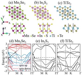 |
| | Fig. 1 The top and side views of the crystal structures of (a) Mn2Se3, (b) In2S3 and (c) TiTe2 monolayers. The band structures of (d) Mn2Se3, (e) In2S3 and (f) TiTe2 monolayers. | |
In the following, we employed TiTe2 as the electrodes, monolayer Mn2Se3 as the spin-filter tunnel barrier and monolayer In2S3 as the tunnel barrier to construct MFTJs. Firstly, the stability of stacking configurations between various materials is considered. By considering the two different ferroelectric polarization states of In2S3, there are twelve possible different stacking configurations of In2S3/Mn2Se3 heterostructures, as shown in Fig. S2.† Besides, six possible different stacking configurations of Mn2Se3/TiTe2 heterostructures are depicted in Fig. S3.† The formation energy (Eform) of the heterostructures can be described as follows:69
| | | Eform = EH − Eupper − Ebottom | (13) |
where
EH is the total energy of the heterostructure, and
Eupper and
Ebottom represent the total energies of upper and bottom monolayers, respectively. The calculated
Eform of In
2S
3/Mn
2Se
3 and Mn
2Se
3/TiTe
2 heterostructures are summarized in Table S1.
† The results reveal that stacking-I of Mn
2Se
3/In
2S
3-P
↑, stacking-V of Mn
2Se
3/In
2S
3-P
↓ and stacking I of Mn
2Se
3/TiTe
2 heterostructures possess the corresponding lowest
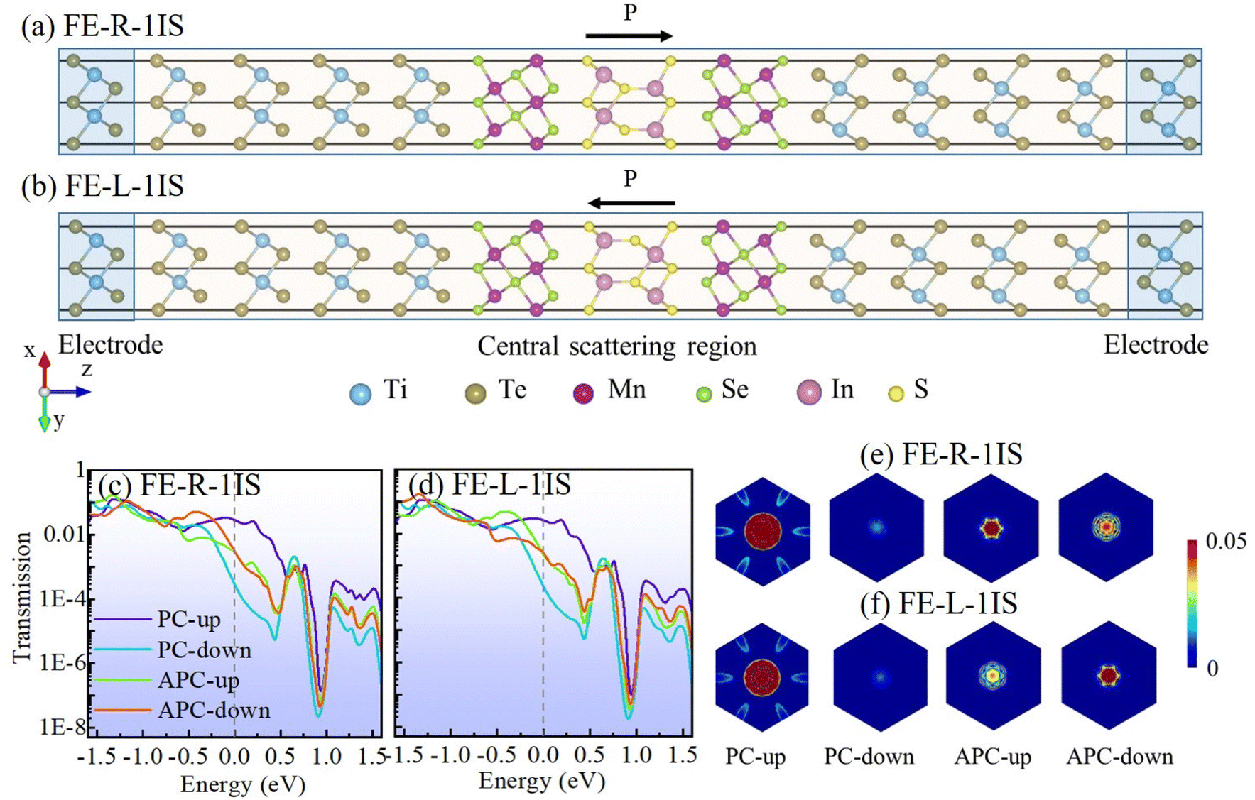
Eform, which indicates that such stacking configurations are the most stable. Therefore, the stacking configurations of different materials in MFTJs are based on the above results. In
Fig. 2(a) and (b), the ferroelectric polarization direction of the monolayer In
2S
3 tunnel barrier can be switched between left and right with an appropriate extra electric field. Herein, the ferroelectric polarizations of monolayer In
2S
3 in MFTJs pointing right and left are namely FE-R-1IS and FE-L-1IS states for short, respectively. Meanwhile, the magnetic arrangements of left and right Mn
2Se
3 layers can be switched to parallel and antiparallel arrangement configurations (PC and APC) with an appropriate extra magnetic field.
 |
| | Fig. 2 The structure schematic diagrams of the MFTJ with (a) FE-R-1IS and (b) FE-L-1IS states. The spin-dependent zero-bias transmission coefficient curves of the MFTJ with (c) FE-R-1IS and (d) FE-L-1IS states. The spin-dependent k||-resolved transmission spectra of the MFTJ with (e) FE-R-1IS and (f) FE-L-1IS states. | |
To reveal the spin-dependent transmission behavior of the MFTJ with FE-R-1IS and FE-L-1IS states, we calculated the spin-dependent zero-bias transmission coefficient curves with the energy region from −1.5 eV to 1.5 eV, as shown in Fig. 2(c) and (d). All the transmission coefficient curves are very similar for the MFTJ with FE-R-1IS and FE-L-1IS states at the energy region below −0.5 eV. When the energy region goes up to around the Fermi level, the spin-up transmission coefficients in PC play a dominant role in the transmission behavior, while spin-down transmission coefficients in PC show a minimal contribution to the transmission behavior. The spin-up and spin-down transmission coefficients exhibit similar medium values around the Fermi level for APC. When the energy region increases to approximately 0.9 eV, all the transmission coefficient curves exhibit a trend of steep decline initially, followed by a rapid rise, resulting in a minimum value near 0.9 eV. The significant differences between the transmission coefficients of PC and APC could contribute to the apparent TMR effect. However, the difference between the transmission coefficient curves of the MFTJ with FE-R-1IS and FE-L-1IS states is not remarkable, which could yield an inconspicuous TER effect.
The spin-dependent k||-resolved transmission spectra at the Fermi level of the MFTJ with FE-R-1IS and FE-L-1IS states are plotted in Fig. 2(e) and (f) to further reveal the spin-dependent transmission behavior. It follows clearly that the MFTJs with such two states share very similar transmission spectra for the same spin state. Therefore, the TER effect can hardly be achieved. In both cases, the spin-up transmission spectra at the Fermi level of PC play a decisive role in the transmission behavior, which agrees with the above discussion well. The spin-up and spin-down transmission spectra at the Fermi level of APC show fewer transmission regions than that of the spin-up channel in PC, but more than that of the spin-down channel in PC. Additionally, the primary spin-up transmission regions of the PC state are located in circular areas for both MFTJs, and there are only minor spin-down transmission regions located at (kx, ky) = (0, 0). On the other hand, although the spin-up and spin-down transmission regions of APC exhibit different shapes, the central transmission regions are predominantly localized around (kx, ky) = (0, 0).
Generally, large TMR and TER ratios are required in MFTJ to ensure optimal device performance.20Table 1 summarizes the different spin-dependent conductances, and TMR and TER ratios calculated according to eqn. (1), (2) and (3), respectively. Interestingly, the spin-up and spin-down conductances of PC reach ∼10−2 and ∼10−4 e2/h levels, respectively, while both spin-up and spin-down conductances of APC are ∼10−3 e2/h levels. Hence the different total conductances of PC and APC can realize the TMR ratios of 448% and 371% for FE-R-1IS and FE-L-1IS MFTJs, respectively, revealing that an apparent TMR effect can be achieved. Unfortunately, the total conductances of PC or APC between FE-R-1IS and FE-L-1IS MFTJs exhibit minor differences. The calculated TER ratios are only 11% and 30% for PC and APC, respectively, indicating that the TER effect is hard to realize in this case for both PC and APC. On the other hand, the calculated SIEs can reach up to near 100% when the MFTJ is in PC, as shown in Table S2;† such high SIEs are essential for the spin information transmission and manipulation.70 Moreover, the RA products can maintain less than 1 Ω μm2 level whether the MFTJ is in PC or APC, as shown in Table S2,† which can satisfy a high recording density of 200 Gbit in−2.71,72 However, owing to the limited TER ratios, such MFTJ with monolayer In2S3 as the tunnel barrier fails to manifest the advantage of MFTJs sufficiently.
Table 1 The calculated transmission coefficients (unit: e2/h), TMR and TER ratios of the MFTJ with FE-R-1IS, and FE-L-1IS states
| MFTJ |
PC state |
APC state |
TMR |
| Spin up |
Spin down |
Total-PC |
Spin up |
Spin down |
Total-APC |
| FE-R-1IS |
2.54 × 10⁻² |
2.21 × 10⁻⁴ |
2.56 × 10⁻² |
2.11 × 10⁻³ |
2.56 × 10⁻³ |
4.68 × 10⁻³ |
448% |
| FE-L-1IS |
2.83 × 10⁻² |
2.78 × 10⁻⁴ |
2.85 × 10⁻² |
3.02 × 10⁻³ |
3.04 × 10⁻³ |
6.06 × 10⁻³ |
371% |
| TERR/L |
|
|
11% |
|
|
30% |
|
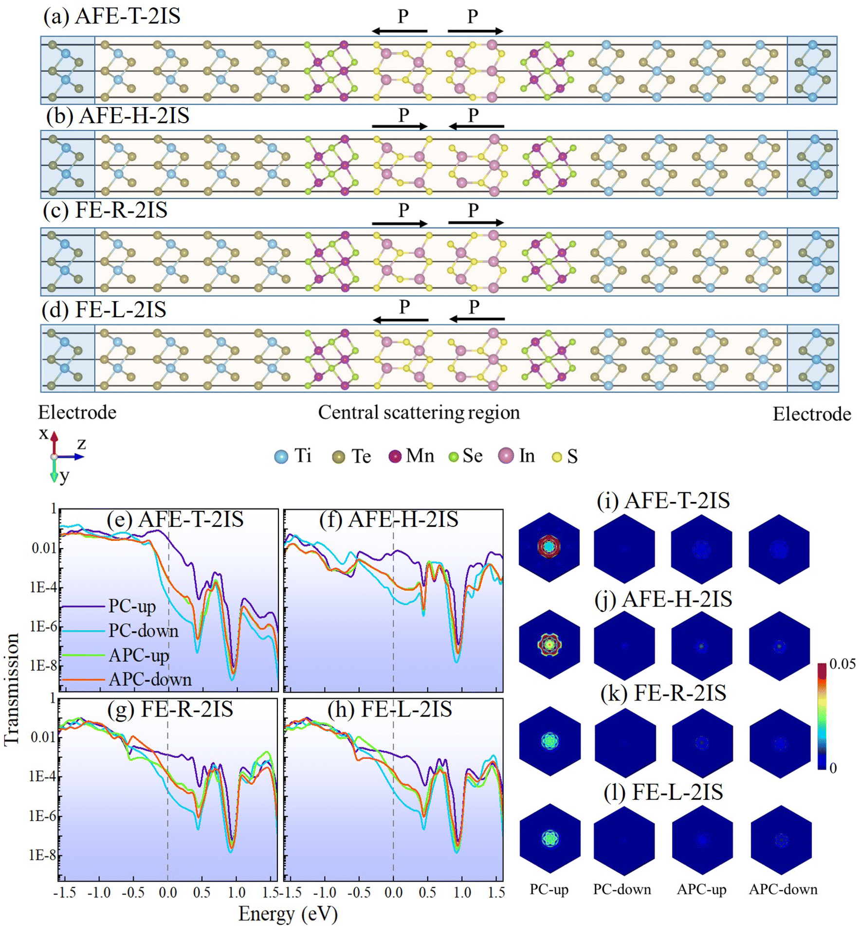
Inspired by the giant tunneling electroresistance effects driven by ferroelectric-antiferroelectric order transitions in bilayer In2S3,42 we further constructed the MFTJs with bilayer In2S3 as the tunnel barrier and investigated the spin-dependent transmission behavior. There are three different kinds of polarization directions in bilayer In2S3, i.e., the tail-to-tail antiferroelectric state and head-to-head antiferroelectric state are namely AFE-T and AFE-H states, as well as the ferroelectric state is namely FE state for short. We considered the different possible stacking configurations for bilayer In2S3 in AFE-T, AFE-H and FE states, as shown in Fig. S4.† The calculated formation energies of various stacking configurations are summarized in Table S3.† In the following, we employed stacking-I to construct the bilayer In2S3 based MFTJs, since stacking-I has the lowest formation energy in most cases. Fig. 3(a–d) depict the various MFTJs by using bilayer In2S3 as the tunnel barrier. Herein, there are two ferroelectric states by considering both the polarization directions of monolayer In2S3 in bilayer In2S3 toward right and left, namely FE-R-2IS and FE-L-2IS states, and that of two antiferroelectric states are namely AFE-T-2IS and AFE-H-2IS states for short, respectively.
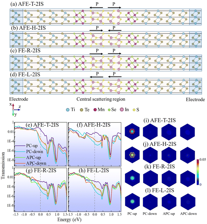 |
| | Fig. 3 The structure schematic diagrams of the MFTJ with (a) AFE-T-2IS, (b) AFE-H-2IS, (c) FE-R-2IS, and (d) FE-L-2IS states. The spin-dependent zero-bias transmission coefficient curves of the MFTJ with (e) AFE-T-2IS, (f) AFE-H-2IS, (g) FE-R-2IS, and (h) FE-L-2IS states. The spin-dependent k||-resolved transmission spectra of the MFTJ with (i) AFE-T-2IS, (j) AFE-H-2IS, (k) FE-R-2IS, and (l) FE-L-2IS states. | |
Fig. 3(e–h) show the spin-dependent zero-bias transmission coefficient curves of the MFTJ with various states using bilayer In2S3 as the tunnel barrier. The shapes of these transmission coefficient curves are similar to the monolayer In2S3 based MFTJ. It is noted that the spin-up transmission coefficient curves in PC show much higher values around the Fermi level. Conversely, the spin-down transmission coefficient curves in the PC display the lowest values around the Fermi level. As for the APC, the spin-up and spin-down transmission coefficient curves demonstrate intermediate values around the Fermi level. Fig. 3(i–l) present the spin-dependent k||-resolved transmission spectra at the Fermi level of the MFTJ with various states for a vivid view. Circular transmission regions are observed in the spin-up transmission spectra of the PC, while minimal transmission regions are found in the transmission spectra of the other three parts. As a result, there is a significant difference in the electronic transmission capacity between the PC and APC, resulting in potential excellent TMR effects. On the other hand, the spin-up channel of PC for the MFTJ with AFE-T-2IS state can be estimated to show a better electronic transmission capacity than that of AFE-H-2IS state. Additionally, the spin-up channels of the PC state for the MFTJ with FE-R-2IS and FE-L-2IS states possess poor electronic transmission capacity. Therefore, apparent TER effects can be observed in the MFTJs with bilayer In2S3 as the tunnel barrier.
To elucidate the physical origin of TMR and TER effects in the devices, the spin-dependent projected local density of states (PLDOSs) of the MFTJ with various states by employing bilayer In2S3 as tunnel barrier are depicted in Fig. 4. The PLDOS of MFTJ with the AFE-T-2IS state in Fig. 4(a) are discussed as an example to reveal the physical origin of the TMR effect. When the magnetic arrangements of two Mn2Se3 layers are in PC, the spin-up electrons from the left electrode only need to overcome the tunnel barrier of bilayer In2S3 to reach the right electrode. Therefore, the spin-up channel in PC owns the highest transmission coefficients. At the same time, it is hard for the spin-down electrons from the left electrode to transfer to the right electrode, since the additional tunnel barriers of the left and right Mn2Se3 layers are required to be overcome. When the magnetic arrangements of two Mn2Se3 layers are in APC, only a few spin-up/spin-down electrons from the left electrode can transfer to the right electrode, since they need to overcome the tunnel barriers of left/right Mn2Se3 layers for spin-up/spin-down electrons. As a result, an apparent TMR effect can be observed when the Mn2Se3 layers are switched between PC and APC. The physical origin of apparent TMRs of the MFJ with AFE-H-2IS, FE-R-2IS and FE-L-2IS states are the same as that of AFE-T-2IS state, as depicted in Fig. 4(b–d). Furthermore, the MTJs still show markedly distinct conductances when two Mn2Se3 layers are in the same magnetic arrangements, which results in an apparent TER effect. Herein, we focus on the spin-up channel of the PC, as it plays a dominant role during transmission. It can be seen clearly that the PLDOS of bilayer In2S3 in the MFTJ with various states shows different behavior when two Mn2Se3 layers are in the same magnetic arrangements. However, it is worth noting that the PLDOS of bilayer In2S3 in two FE states (i.e., FE-R-2IS and FE-L-2IS) are mirror symmetric due to the opposite polarization directions of bilayer In2S3, resulting in little difference between their conductances. In other words, the FE-R-2IS and FE-L-2IS states can be regarded as one FE state. Therefore, the TER effect results from the switching bilayer In2S3 between AFE-T-2IS, AFE-H-2IS and FE (FE-R-2IS and FE-L-2IS) states.
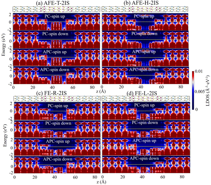 |
| | Fig. 4 The spin-dependent projected local density of states (PLDOSs) of the MFTJ with (a) AFE-T-2IS, (b) AFE-H-2IS, (c) FE-R-2IS and (d) FE-L-2IS states. | |
To get a detailed insight into the performance of MFTJ with bilayer In2S3 as the tunnel barrier, Table 2 summarizes the different spin-dependent conductances, TMR and TER ratios. The calculated TMR ratios of the MFTJ with FE-R-2IS and FE-L-2IS states are 312% and 336%, respectively. Excitingly, the TMR ratios of MFTJ with AFE-T-2IS and AFE-H-2IS states show superior TMR effects up to 5698% and 1454%, respectively. On the other hand, when the MFTJ is in the PC, the large TER ratios of 1771% and 360% can be achieved during the MFTJ with AFE-T-2IS and AFE-H-2IS states switching to FE-L-2IS state, respectively. As shown in Table S4,† SIE for the MFTJ with all states can reach near 100% when the MFTJ is in the PC, and the MFTJ with AFE-T-2IS and AFE-H-2IS states can obtain the low RA product of less than 1 Ω μm2. Furthermore, we calculated the spin-dependent conductance by applying voltages to explore the spin-dependent conductance in non-equilibrium situations. The results are shown in Table 3, Tables S5–S7 and Fig. S5.† It is noted that the spin-dependent conductance in PC state show a larger difference than the conductance in APC state, which results in the increasing of TMR ratio at the finite bias of 20 meV. As a result, we can achieve the maximum TMR ratio of 6237% by applying 20 meV bias. However, it is a pity that the TER ratios decrease with the finite bias increasing. Therefore, the MFTJs with bilayer In2S3 as the tunnel barrier can realize excellent TMR and TER effects, revealing potential applications in nonvolatile memory devices.
Table 2 The spin-dependent conductance (unit: e2/h), TMR and TER ratios of the MFTJ with AFE-T-2IS, AFE-H-2IS, FE-R-2IS and FE-L-2IS states under zero bias
| MFTJ |
PC state |
APC state |
TMR |
| Spin up |
Spin down |
Total-PC |
Spin up |
Spin down |
Total-APC |
| AFE-T-2IS |
2.66 × 10⁻² |
2.54 × 10⁻⁵ |
2.66 × 10⁻² |
2.25 × 10⁻⁴ |
2.34 × 10⁻⁴ |
4.59 × 10⁻⁴ |
5698% |
| AFE-H-2IS |
6.50 × 10⁻³ |
3.28 × 10⁻⁵ |
6.53 × 10⁻³ |
1.88 × 10⁻⁴ |
2.32 × 10⁻⁴ |
4.20 × 10⁻⁴ |
1454% |
| FE-R-2IS |
1.39 × 10⁻³ |
1.93 × 10⁻⁵ |
1.41 × 10⁻³ |
2.03 × 10⁻⁴ |
1.40 × 10⁻⁴ |
3.42 × 10⁻⁴ |
312% |
| FE-L-2IS |
1.40 × 10⁻³ |
1.95 × 10⁻⁵ |
1.42 × 10⁻³ |
1.19 × 10⁻⁴ |
2.07 × 10⁻⁴ |
3.26 × 10⁻⁴ |
336% |
| TERAFE-T/FE-L |
|
|
1771% |
|
|
41% |
|
| TER AFE-H/FE-L |
|
|
360% |
|
|
29% |
|
| TER FE-R/FE-L |
|
|
1% |
|
|
5% |
|
Table 3 The spin-dependent conductance (unit: e2/h), TMR and TER ratios of the MFTJ with AFE-T-2IS, AFE-H-2IS, FE-R-2IS and FE-L-2IS states under the bias of 20 meV
| MFTJ |
PC state |
APC state |
TMR |
| Spin up |
Spin down |
Total-PC |
Spin up |
Spin down |
Total-APC |
| AFE-T-2IS |
2.52 × 10⁻² |
2.44 × 10⁻⁵ |
2.52 × 10⁻² |
2.00 × 10⁻⁴ |
1.98 × 10⁻⁴ |
3.98 × 10⁻⁴ |
6237% |
| AFE-H-2IS |
6.66 × 10⁻³ |
2.68 × 10⁻⁵ |
6.69 × 10⁻³ |
1.54 × 10⁻⁴ |
1.52 × 10⁻⁴ |
3.06 × 10⁻⁴ |
2085% |
| FE-R-2IS |
1.39 × 10⁻³ |
1.54 × 10⁻⁵ |
1.40 × 10⁻³ |
1.42 × 10⁻⁴ |
9.35 × 10⁻⁴ |
2.35 × 10⁻⁴ |
497% |
| FE-L-2IS |
1.40 × 10⁻³ |
1.61 × 10⁻⁵ |
1.42 × 10⁻³ |
1.10 × 10⁻⁴ |
1.47 × 10⁻⁴ |
2.57 × 10⁻⁴ |
451% |
| TERAFE-T/FE-L |
|
|
1682% |
|
|
55% |
|
| TERAFE-H/FE-L |
|
|
373% |
|
|
19% |
|
| TERFE-R/FE-L |
|
|
1% |
|
|
8% |
|
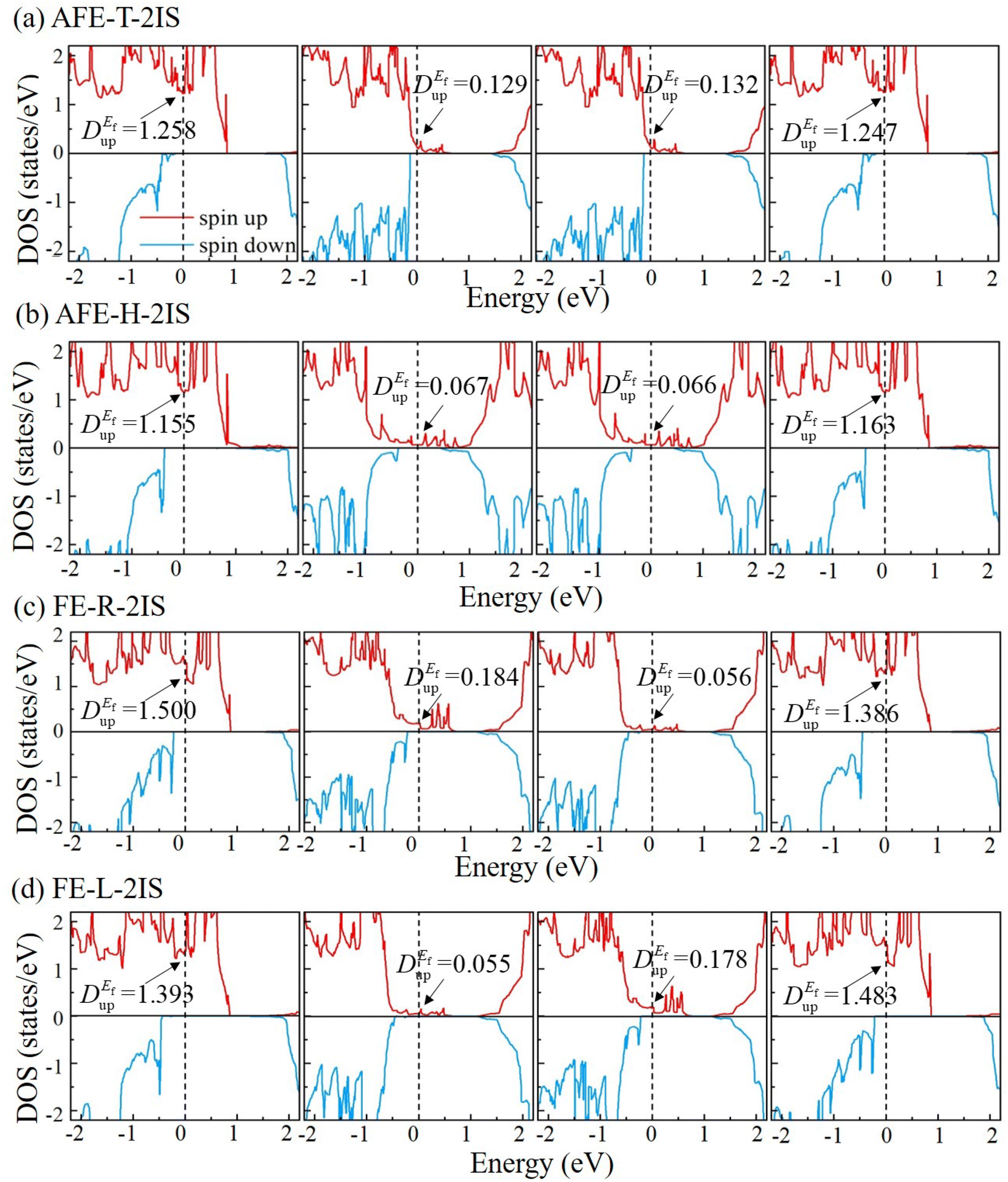
According to our previous results, the spin-up channels of these MFTJs in PC states play a dominant role in the TER ratios. To further unravel why the spin-up channels of various MFTJs in PC states exhibit different electronic transmission capacities, we calculated the spin-dependent projected density of states (PDOS) and projected band structures of Mn2Se3/bilayer In2S3/Mn2Se3 multilayers, as depicted in Fig. 5 and Fig. S6–S9.† The left and right Mn2Se3 layers show excellent conductivity since they possess a high value of spin-up PDOS at the Fermi level. As a result, the differences of electronic transmission capacity in the spin-up channels are derived from the PDOS of In2S3 layers. For the MFTJ with AFE-T-2IS state in Fig. 5(a), the left and right In2S3 layers show the spin-up PDOS of 0.129 and 0.132 states per eV at the Fermi level, respectively, indicating a good device conductivity. For the MFTJ with AFE-H-2IS state in Fig. 5(b), the spin-up PDOS of the left and right In2S3 layers at the Fermi level are only 0.067 and 0.066 states per eV, respectively, revealing a poor device conductivity. For the MFTJ with FE-R-2IS states in Fig. 5(c), although the spin-up PDOS of left In2S3 at the Fermi level shows a high value of 0.184 states per eV, the device conductivity is limited by the spin-up PDOS of right In2S3 at the Fermi level of 0.056 states per eV. For the MFTJ with FE-L-2IS state in Fig. 5(d), the spin-up PDOS of left In2S3 at the Fermi level are only 0.055 states per eV, resulting in poor conductivity.
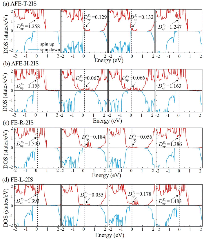 |
| | Fig. 5 The spin-dependent DOS of the Mn2Se3/bilayer-In2S3/Mn2Se3 part in the MFTJ with (a) AFE-T-2IS, (b) AFE-H-2IS, (c) FE-R-2IS and (d) FE-L-2IS states. DEfup represents the spin-up DOS value at the Fermi level. | |
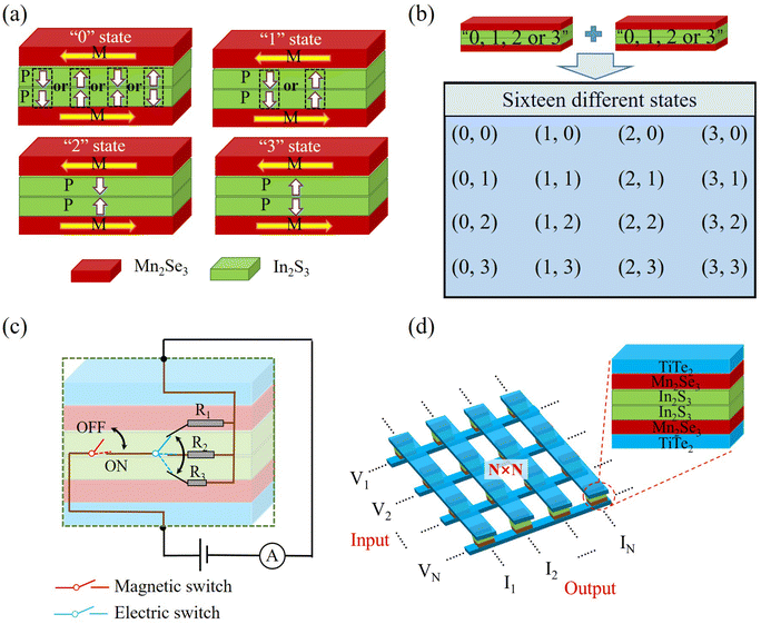
Based on these results, certain applications may be envisaged using such MFTJ with bilayer In2S3 as the tunnel barrier in data storage devices. It is noted that a dual gate is an effective device structure to realize reversible switching between FE and AFE states.42,73 There are eight states in the MFTJ at different ferromagnetic and ferroelectric situations, as shown in Fig. 6(a): two ferromagnetic layers controlled by magnetic field can realize PC and APC, two ferroelectric layers controlled by electric field can achieve AFE-T-2IS, AFE-H-2IS, FE-R-2IS and FE-L-2IS states. Herein, four APC states can be degenerated to one storage state, namely “0” state, since these states are insensitive to the ferroelectric polarization configurations (see the Total-APC in Table 2). On the other hand, when two layers of Mn2Se3 are in PC and the polarization directions of bilayer In2S3 toward the left or right simultaneously, the MFTJ exhibits equivalent resistances. Therefore, four PC states can be degenerated to three different storage states, namely “1”, “2” and “3” states. As a result, four distinguishable storage states (i.e., “0”, “1”, “2” and “3” states) reveal that a multilevel nonvolatile storage can be achieved in the MFTJ. As depicted in Fig. 6(b), sixteen different storage states can be achieved in terms of only two MFTJ units, which reveals the significant advantages of utilizing such MFTJ for data storage. It is interesting to note that the ferromagnetic and ferroelectric transitions in the proposed MFTJs with bilayer In2S3 as the tunnel barrier are mutually independent. Therefore, it is possible to achieve logical in-memory computing without losing the stored data in only one MFTJ unit. As shown in Fig. 6(c), the external magnetic field can switch the MFTJ between PC and APC states, corresponding to the high and low electrical level, respectively. Hence the effect of the external magnetic field acts as an equivalent magnetic switch in the circuit to realize the “ON” and “OFF” logic operation switching. At the same time, the switch of external electric fields can realize three different conductance states, which is equivalent to an electric switch toggles between R1, R2 and R3. As a result, the magnetic switch service controls the “ON” and “OFF” states for logic calculations, while three different conductance states switched by the electric polarization can be utilized for the multilevel storage. Herein, the calculations realized by the magnetic switch do not affect the storage data achieved by the electric switch. It is worth noting that these storage states are non-volatile, since the resistance and magnetoresistance can be retained when the applied electric and magnetic fields disappear. Fig. 6(d) depicts the proposed in-memory computing device, which consists of an N × N array. Each storage unit is arranged in a cross-shaped matrix configuration for computation. When a voltage vector is applied to one end of the cross matrix, the resulting current vector at the other end is the product of the applied voltage vector and the conductivity of each unit.74 In this way, the multiplication and accumulation operation of vectors and matrices can be achieved.
 |
| | Fig. 6 The multilevel storage mechanism of (a) four distinguishable conductance states in a MFTJ unit, and (b) sixteen different states achieved by two series MFTJ units. The in-memory computing application mechanism of (c) the equivalent circuit diagram for magnetic and electric switch, (d) the N × N MFTJ array units. | |
Conclusion
In summary, based on density functional theory and non-equilibrium Green's function method, the crystal and electronic structures of Mn2Se3, In2S3 and TiTe2 monolayers were investigated. It turns out that Mn2Se3, In2S3 and TiTe2 monolayers are a ferromagnetic material with half-metallicity, a ferroelectric material with semiconducting behavior and a metal material, respectively. We employed multilayer TiTe2 as the electrodes, monolayer Mn2Se3 as the spin-filter tunnel barrier and In2S3 layers as the tunnel barrier to construct multiferroic tunnel junctions (MFTJs). It reveals that the MFTJ with monolayer In2S3 as the tunnel barrier can achieve an apparent TMR effect with the maximum TMR ratio of 448%, while the TER effect is hard to realize. Interestingly, both apparent TMR and TER effects can be achieved in the MFTJ with bilayer In2S3 as the tunnel barrier. The maximum TMR and TER ratios can reach up to 6237% and 1771% under finite bias, respectively. Furthermore, four distinguishable storage states (i.e., “0”, “1”, “2” and “3” states) reveal that multilevel storage can be achieved in such a MFTJ. Moreover, the effect of external magnetic and electric fields can act as equivalent magnetic and electric switches. The “ON” and “OFF” states are controlled by the magnetic switch service for logic calculations, while three different conductance states switched by the electric polarization can be utilized for the multilevel storage. The storage and computing integration can be achieved by arranging multiple MFTJs into an N × N array. These findings demonstrate that such MFTJs with bilayer In2S3 as the tunnel barrier might have good potential applications for multilevel nonvolatile storage and in-memory computing devices.
Conflicts of interest
The authors declare no competing financial interest.
Acknowledgements
This work was supported by the National Key Research and Development Program of China (No. 2022YFB3807200), the National Natural Science Foundation of China (No. 21973012), the Natural Science Foundation of Fujian Province (No. 2021J06011, 2021H6011 and 2021J01590), and the “Qishan Scholar” Scientific Research Project of Fuzhou University.
References
- K. Roy, A. Jaiswal and P. Panda, Towards spike-based machine intelligence with neuromorphic computing, Nature, 2019, 575, 607–617 CrossRef CAS PubMed.
- M. Lanza, A. Sebastian, W. D. Lu, M. Le Gallo, M. F. Chang, D. Akinwande, F. M. Puglisi, H. N. Alshareef, M. Liu and J. B. Roldan, Memristive technologies for data storage, computation, encryption, and radio-frequency communication, Science, 2022, 376, eabj9979 CrossRef CAS PubMed.
- G. Milano, M. Aono, L. Boarino, U. Celano, T. Hasegawa, M. Kozicki, S. Majumdar, M. Menghini, E. Miranda, C. Ricciardi, S. Tappertzhofen, K. Terabe and I. Valov, Quantum Conductance in Memristive Devices: Fundamentals, Developments, and Applications, Adv. Mater., 2022, 34, e2201248 CrossRef PubMed.
- A. Zador, S. Escola, B. Richards, B. Ölveczky, Y. Bengio, K. Boahen, M. Botvinick, D. Chklovskii, A. Churchland, C. Clopath, J. DiCarlo, S. Ganguli, J. Hawkins, K. Körding, A. Koulakov, Y. LeCun, T. Lillicrap, A. Marblestone, B. Olshausen, A. Pouget, C. Savin, T. Sejnowski, E. Simoncelli, S. Solla, D. Sussillo, A. S. Tolias and D. Tsao, Catalyzing next-generation Artificial Intelligence through NeuroAI, Nat. Commun., 2023, 14, 1597 CrossRef CAS PubMed.
- B. Dieny, I. L. Prejbeanu, K. Garello, P. Gambardella, P. Freitas, R. Lehndorff, W. Raberg, U. Ebels, S. O. Demokritov, J. Akerman, A. Deac, P. Pirro, C. Adelmann, A. Anane, A. V. Chumak, A. Hirohata, S. Mangin, S. O. Valenzuela, M. C. Onbaşlı, M. d'Aquino, G. Prenat, G. Finocchio, L. Lopez-Diaz, R. Chantrell, O. Chubykalo-Fesenko and P. Bortolotti, Opportunities and challenges for spintronics in the microelectronics industry, Nat. Electron., 2020, 3, 446–459 CrossRef.
- F. Wu, C. Lu, M. Zhu, H. Chen, J. Zhu, K. Yu, L. Li, M. Li, Q. Chen, X. Li, X. Cao, Z. Wang, Z. Zha, Y. Zhuang and Y. Pan, Towards a new generation of artificial intelligence in China, Nat. Mach. Intell., 2020, 2, 312–316 CrossRef.
- T. Kimura, T. Goto, H. Shintani, K. Ishizaka, T. Arima and Y. Tokura, Magnetic control of ferroelectric polarization, Nature, 2003, 426, 55–58 CrossRef CAS PubMed.
- H. Wang and X. Qian, Two-dimensional multiferroics in monolayer group IV monochalcogenides, 2D Mater., 2017, 4, 015042 CrossRef.
- H. X. Liu, Y. Honda, T. Taira, K. I. Matsuda, M. Arita, T. Uemura and M. Yamamoto, Giant tunneling magnetoresistance in epitaxial Co2MnSi/MgO/Co2MnSi magnetic tunnel junctions by half-metallicity of Co2MnSi and coherent tunneling, Appl. Phys. Lett., 2012, 101, 132418 CrossRef.
- T. Miyazaki and N. Tezuka, Giant magnetic tunneling effect in Fe/Al2O3/Fe junction, J. Magn. Magn. Mater., 1995, 139, L231–L234 CrossRef CAS.
- P. Vlaic, N. Baadji, M. Alouani, H. Dreyssé, O. Eriksson, O. Bengone and I. Turek, Calculated electronic and transport properties of Fe/GaAs/Fe(001) tunnel junctions, Surf. Sci., 2004, 566–568, 303–308 CrossRef CAS.
- Z. Cui, H. Ding and Y. Feng, Investigation of the half-metallicity, magnetism and spin transport properties of double half-Heusler alloys Mn2CoCrZ2 (Z = P, As), Phys. Chem. Chem. Phys., 2021, 23, 17984–17991 RSC.
- S. Yuasa, T. Nagahama and Y. Suzuki, Spin-polarized resonant tunneling in magnetic tunnel junctions, Science, 2002, 297, 234–237 CrossRef CAS PubMed.
- S. Yuasa, T. Nagahama, A. Fukushima, Y. Suzuki and K. Ando, Giant room-temperature magnetoresistance in single-crystal Fe/MgO/Fe magnetic tunnel junctions, Nat. Mater., 2004, 3, 868–871 CrossRef CAS PubMed.
- A. Gruverman, D. Wu, H. Lu, Y. Wang, H. W. Jang, C. M. Folkman, M. Ye. Zhuravlev, D. Felker, M. Rzchowski, C. B. Eom and E. Y. Tsymbal, Tunneling Electroresistance Effect in Ferroelectric Tunnel Junctions at the Nanoscale, Nano Lett., 2009, 9, 3539–3543 CrossRef CAS PubMed.
- X. Liu, J. D. Burton and E. Y. Tsymbal, Enhanced Tunneling Electroresistance in Ferroelectric Tunnel Junctions due to the Reversible Metallization of the Barrier, Phys. Rev. Lett., 2016, 116, 197602 CrossRef PubMed.
- Z. Cui, T. Li, R. Xiong, C. Wen, Y. Zhang, J. Zheng, B. Wu and B. Sa, The giant tunneling electroresistance effect in monolayer In2SSeTe-based lateral ferroelectric tunnel junctions, Mater. Adv., 2023, 4, 1572–1582 RSC.
- E. Y. Tsymbal, A. Gruverman, V. Garcia, M. Bibes and A. Barthélémy, Ferroelectric and multiferroic tunnel junctions, MRS Bull., 2012, 37, 138–143 CrossRef CAS.
- D. Pantel, S. Goetze, D. Hesse and M. Alexe, Reversible electrical switching of spin polarization in multiferroic tunnel junctions, Nat. Mater., 2012, 11, 289–293 CrossRef CAS PubMed.
- Y. W. Yin, M. Raju, W. J. Hu, X. J. Weng, K. Zou, J. Zhu, X. G. Li, Z. D. Zhang and Q. Li, Multiferroic tunnel junctions, Front. Phys., 2012, 7, 380–385 CrossRef.
- M. Y. Zhuravlev, S. S. Jaswal, E. Y. Tsymbal and R. F. Sabirianov, Ferroelectric switch for spin injection, Appl. Phys. Lett., 2005, 87, 222114 CrossRef.
- V. Garcia, M. Bibes, L. Bocher, S. Valencia, F. Kronast, A. Crassous, X. Moya, S. Enouz-Vedrenne, A. Gloter, D. Imhoff, C. Deranlot, N. D. Mathur, S. Fusil, K. Bouzehouane and A. Barthélémy, Ferroelectric Control of Spin Polarization, Science, 2010, 327, 1106–1110 CrossRef CAS PubMed.
- C. G. Duan, S. S. Jaswal and E. Y. Tsymbal, Predicted magnetoelectric effect in Fe/BaTiO3 multilayers: ferroelectric control of magnetism, Phys. Rev. Lett., 2006, 97, 047201 CrossRef PubMed.
- J. P. Velev, C. G. Duan, J. D. Burton, A. Smogunov, M. K. Niranjan, E. Tosatti, S. S. Jaswal and E. Y. Tsymbal, Magnetic Tunnel Junctions with Ferroelectric Barriers: Prediction of Four Resistance States from First Principles, Nano Lett., 2009, 9, 427–432 CrossRef CAS PubMed.
- H. M. Yau, Z. B. Yan, N. Y. Chan, K. Au, C. M. Wong, C. W. Leung, F. Y. Zhang, X. S. Gao and J. Y. Dai, Low-field Switching Four-state Nonvolatile Memory Based on Multiferroic Tunnel Junctions, Sci. Rep., 2015, 5, 12826 CrossRef CAS PubMed.
- A. Quindeau, I. Fina, X. Marti, G. Apachitei, P. Ferrer, C. Nicklin, E. Pippel, D. Hesse and M. Alexe, Four-state ferroelectric spin-valve, Sci. Rep., 2015, 5, 9749 CrossRef CAS PubMed.
- Y. Yin and Q. Li, A review on all-perovskite multiferroic tunnel junctions, J. Materiomics, 2017, 3, 245–254 CrossRef.
- B. Peng, Q. Zhang, X. Li, T. Sun, H. Fan, S. Ke, M. Ye, Y. Wang, W. Lu, H. Niu, J. F. Scott, X. Zeng and H. Huang, Giant Electric Energy Density in Epitaxial Lead-Free Thin Films with Coexistence of Ferroelectrics and Antiferroelectrics, Adv. Electron. Mater., 2015, 1, 1500052 CrossRef.
- W. Huang, Y. Lin, Y. Yin, L. Feng, D. Zhang, W. Zhao, Q. Li and X. Li, Interfacial Ion Intermixing Effect on Four-Resistance States in La0.7Sr0.3MnO3/BaTiO3/La0.7Sr0.3MnO3 Multiferroic Tunnel Junctions, ACS Appl. Mater. Interfaces, 2016, 8, 10422–10429 CrossRef CAS PubMed.
- J. Ruan, X. Qiu, Z. Yuan, D. Ji, P. Wang, A. Li and D. Wu, Improved memory functions in multiferroic tunnel junctions with a dielectric/ferroelectric composite barrier, Appl. Phys. Lett., 2015, 107, 232902 CrossRef.
- V. Garcia, M. Bibes, L. Bocher, S. Valencia, F. Kronast, A. Crassous, X. Moya, S. Enouz-Vedrenne, A. Gloter, D. Imhoff, C. Deranlot, N. D. Mathur, S. Fusil, K. Bouzehouane and A. Barthélémy, Ferroelectric control of spin polarization, Science, 2010, 327, 1106–1110 CrossRef CAS PubMed.
- F. Gao, Y. Zhao, X. Zhang and J. You, Recent Progresses on Defect Passivation toward Efficient Perovskite Solar Cells, Adv. Energy Mater., 2019, 10, 1902650 CrossRef.
- K. S. Novoselov, A. K. Geim, S. V. Morozov, D. Jiang, Y. Zhang, S. V. Dubonos, I. V. Grigorieva and A. A. Firsov, Electric Field Effect in Atomically Thin Carbon Films, Science, 2004, 306, 666–669 CrossRef CAS PubMed.
- K. S. Burch, D. Mandrus and J. G. Park, Magnetism in two-dimensional van der Waals materials, Nature, 2018, 563, 47–52 CrossRef CAS PubMed.
- D. L. Duong, S. J. Yun and Y. H. Lee, van der Waals Layered Materials: Opportunities and Challenges, ACS Nano, 2017, 11, 11803–11830 CrossRef CAS PubMed.
- K. S. Novoselov, A. Mishchenko, A. Carvalho and A. H. Castro Neto, 2D materials and van der Waals heterostructures, Science, 2016, 353, aac9439 CrossRef CAS PubMed.
- M. Gibertini, M. Koperski, A. F. Morpurgo and K. S. Novoselov, Magnetic 2D materials and heterostructures, Nat. Nanotechnol., 2019, 14, 408–419 CrossRef CAS PubMed.
- Y. Su, X. Li, M. Zhu, J. Zhang, L. You and E. Y. Tsymbal, van der Waals Multiferroic Tunnel Junctions, Nano Lett., 2021, 21, 175–181 CrossRef CAS PubMed.
- H. Bai, X. Li, H. Pan, P. He, Z. A. Xu and Y. Lu, van der Waals Antiferroelectric Magnetic Tunnel Junction: A First-Principles Study of a CrSe2/CuInP2S6/CrSe2 Junction, ACS Appl. Mater. Interfaces, 2021, 13, 60200–60208 CrossRef CAS PubMed.
- C. C. Chiang, V. Ostwal, P. Wu, C. S. Pang, F. Zhang, Z. Chen and J. Appenzeller, Memory applications from 2D materials, Appl. Phys. Rev., 2021, 8, 021306 CAS.
- C. Yu, X. Li, X. Li and J. Yang, High Curie Temperature and Intrinsic Ferromagnetic Half-Metallicity in Mn2X3 (X = S, Se, Te) Nanosheets, J. Phys. Chem. Lett., 2021, 12, 11790–11794 CrossRef CAS PubMed.
- J. Ding, D. F. Shao, M. Li, L. W. Wen and E. Y. Tsymbal, Two-Dimensional Antiferroelectric Tunnel Junction, Phys. Rev. Lett., 2021, 126, 057601 CrossRef CAS PubMed.
- Z. Yan, Z. Li, Y. Han, Z. Qiao and X. Xu, Giant tunneling magnetoresistance and electroresistance in α-In2Se3-based van der Waals multiferroic tunnel junctions, Phys. Rev. B, 2022, 105, 075423 CrossRef CAS.
- L. Kang, P. Jiang, H. Hao, Y. Zhou, X. Zheng, L. Zhang and Z. Zeng, Giant tunneling electroresistance in two-dimensional ferroelectric tunnel junctions with out-of-plane ferroelectric polarization, Phys. Rev. B, 2020, 101, 014105 CrossRef CAS.
- Z. Liu, P. Hou, L. Sun, E. Y. Tsymbal, J. Jiang and Q. Yang, In-plane ferroelectric tunnel junctions based on 2D α-In2Se3/semiconductor heterostructures, npj Comput. Mater., 2023, 9, 6 CrossRef CAS.
- G. Zhang, K. Lu, Y. Wang, H. Wang and Q. Chen, Mechanical and electronic properties of α-M2X3(M=Ga, In; X=S, Se) monolayers, Phys. Rev. B, 2022, 105, 235303 CrossRef CAS.
- G. Liu, T. Chen, G. Zhou, Z. Xu and X. Xiao, Nonvolatile Electrical Control and Reversible Gas Capture by Ferroelectric Polarization Switching in 2D FeI2/In2S3 van der Waals Heterostructures, ACS Sens., 2023, 8, 1440–1449 CrossRef CAS PubMed.
- G. Wang, K. Li, L. Peng, Y. Zhang, J. Zhou and Z. Sun, High-Throughput Automatic Integrated Material Calculations and Data Management Intelligent Platform and the Application in Novel Alloys, Acta Metall. Sin., 2022, 58, 75–88 CAS.
- G. Wang, L. Peng, K. Li, L. Zhu, J. Zhou, N. Miao and Z. Sun, ALKEMIE: An intelligent computational platform for accelerating materials discovery and design, Comput. Mater. Sci., 2021, 186, 110064 CrossRef CAS.
- G. Kresse and J. Furthmüller, Efficient iterative schemes for ab initio total-energy calculations using a plane-wave basis set, Phys. Rev. B: Condens. Matter Mater. Phys., 1996, 54, 11169 CrossRef CAS PubMed.
- G. Kresse and J. Furthmüller, Efficiency of ab initio total energy calculations for metals and semiconductors using a plane-wave basis set, Comput. Mater. Sci., 1996, 6, 15–50 CrossRef CAS.
- J. P. Perdew, K. Burke and M. Ernzerhof, Generalized Gradient Approximation Made Simple, Phys. Rev. Lett., 1996, 77, 3865 CrossRef CAS PubMed.
- S. Grimme, J. Antony, S. Ehrlich and H. Krieg, A consistent and accurate ab initio parametrization of density functional dispersion correction (DFT-D) for the 94 elements H-Pu, J. Chem. Phys., 2010, 132, 154104 CrossRef PubMed.
- L. Bengtsson, Dipole correction for surface supercell calculations, Phys. Rev. B: Condens. Matter Mater. Phys., 1999, 59, 12301 CrossRef CAS.
- M. Brandbyge, J. L. Mozos, P. Ordejón, J. Taylor and K. Stokbro, Density-functional method for nonequilibrium electron transport, Phys. Rev. B: Condens. Matter Mater. Phys., 2002, 65, 165401 CrossRef.
- S. Smidstrup, T. Markussen, P. Vancraeyveld, J. Wellendorff, J. Schneider, T. Gunst, B. Verstichel, D. Stradi, P. A. Khomyakov, U. G. Vej-Hansen, M. E. Lee, S. T. Chill, F. Rasmussen, G. Penazzi, F. Corsetti, A. Ojanpera, K. Jensen, M. L. N. Palsgaard, U. Martinez, A. Blom, M. Brandbyge and K. Stokbro, QuantumATK: an integrated platform of electronic and atomic-scale modelling tools, J. Phys.: Condens. Matter, 2020, 32, 015901 CrossRef CAS PubMed.
- M. J. van Setten, M. Giantomassi, E. Bousquet, M. J. Verstraete, D. R. Hamann, X. Gonze and G. M. Rignanese, The PseudoDojo: Training and grading a 85 element optimized norm-conserving pseudopotential table, Comput. Phys. Commun., 2018, 226, 39–54 CrossRef CAS.
- V. Blum, R. Gehrke, F. Hanke, P. Havu, V. Havu, X. Ren, K. Reuter and M. Scheffler, Ab initio molecular simulations with numeric atom-centered orbitals, Comput. Phys. Commun., 2009, 180, 2175–2196 CrossRef CAS.
- A. R. Rocha, V. M. García-Suárez, S. Bailey, C. Lambert, J. Ferrer and S. Sanvito, Spin and molecular electronics in atomically generated orbital landscapes, Phys. Rev. B: Condens. Matter Mater. Phys., 2006, 73, 085414 CrossRef.
- Y. Meir and N. S. Wingreen, Landauer formula for the current through an interacting electron region, Phys. Rev. Lett., 1992, 68, 2512–2515 CrossRef PubMed.
- J. P. Velev, C. G. Duan, J. D. Burton, A. Smogunov, M. K. Niranjan, E. Tosatti, S. S. Jaswal and E. Y. Tsymbal, Magnetic Tunnel Junctions with Ferroelectric Barriers: Prediction of Four Resistance States from First Principles, Nano Lett., 2009, 9, 427–432 CrossRef CAS PubMed.
- Q. Zhang, Y. Cheng and U. Schwingenschlögl, Series of topological phase transitions in TiTe2 under strain, Phys. Rev. B: Condens. Matter Mater. Phys., 2013, 88, 155317 CrossRef.
- Y. Arnaud and M. Chevreton, Etude comparative des composés TiX2 (X = S, Se, Te). Structures de TiTe2 et TiSeTe, J. Solid State Chem., 1981, 39, 230–239 CrossRef CAS.
- M. K. Lin, T. He, J. A. Hlevyack, P. Chen, S. K. Mo, M. Y. Chou and T. C. Chiang, Coherent Electronic Band Structure of TiTe2/TiSe2 Moire Bilayer, ACS Nano, 2021, 15, 3359–3364 CrossRef CAS PubMed.
- P. Chen, W. W. Pai, Y. H. Chan, A. Takayama, C. Z. Xu, A. Karn, S. Hasegawa, M. Y. Chou, S. K. Mo, A. V. Fedorov and T. C. Chiang, Emergence of charge density waves and a pseudogap in single-layer TiTe2, Nat. Commun., 2017, 8, 516 CrossRef CAS PubMed.
- R. Li, J. Jiang, W. Mi and H. Bai, Ferroelectric polarization tailored interfacial charge distribution to modify magnetic properties of two-dimensional Janus FeBrI/In2S3 heterostructures, Appl. Phys. Lett., 2022, 120, 162401 CrossRef CAS.
- R. Li, J. Jiang, W. Mi and H. Bai, Ferroelectric polarization tailored interfacial charge distribution to modify magnetic properties of two-dimensional Janus FeBrI/In2S3 heterostructures, Appl. Phys. Lett., 2022, 120, 162401 CrossRef CAS.
- Y. Arnaud and M. Chevreton, Etude comparative des composés TiX2 (X = S, Se, Te). Structures de TiTe2 et TiSeTe, J. Solid State Chem., 1981, 39, 230–239 CrossRef CAS.
- J. Liao, B. Sa, J. Zhou, R. Ahuja and Z. Sun, Design of High-Efficiency Visible-Light Photocatalysts for Water Splitting: MoS2/AlN(GaN) Heterostructures, J. Phys. Chem. C, 2014, 118, 17594–17599 CrossRef CAS.
- Y. Liu, C. Zeng, J. Zhong, J. Ding, Z. M. Wang and Z. Liu, Spintronics in Two-Dimensional Materials, Nanomicro Lett., 2020, 12, 93 CrossRef CAS.
- Y. Nagamine, H. Maehara, K. Tsunekawa, D. D. Djayaprawira, N. Watanabe and S. Y. K. Ando, Ultralow resistance-area product of 0.4 Ω(μm)2 and high magnetoresistance above 50% in CoFeB/MgO/CoFeB magnetic tunnel junctions, Appl. Phys. Lett., 2006, 89, 162507 CrossRef.
- H. Maehara, K. Nishimura, Y. Nagamine, K. Tsunekawa, T. Seki, H. Kubota, A. Fukushima, K. Yakushiji, K. Ando and S. Yuasa, Tunnel Magnetoresistance above 170% and Resistance–Area Product of 1Ω(μm)2 Attained by In situ Annealing of Ultra-Thin MgO Tunnel Barrier, Appl. Phys. Express, 2011, 4, 033002 CrossRef.
- M. J. Spijkman, K. Myny, E. C. P. Smits, P. Heremans, P. W. M. Blom and D. M. de Leeuw, Dual–Gate Thin–Film Transistors, Integrated Circuits and Sensors, Adv. Mater., 2011, 23, 3231–3242 CrossRef CAS PubMed.
- R. Berdan, T. Marukame, K. Ota, M. Yamaguchi, M. Saitoh, S. Fujii, J. Deguchi and Y. Nishi, Low-power linear computation using nonlinear ferroelectric tunnel junction memristors, Nat. Electron., 2020, 3, 259–266 CrossRef.
|
| This journal is © The Royal Society of Chemistry 2024 |
Click here to see how this site uses Cookies. View our privacy policy here. 
 *a,
Kan-Hao
Xue
*a,
Kan-Hao
Xue

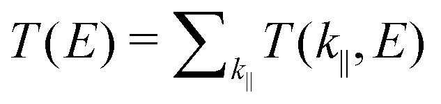 is the k-point averaged transmission function at energy E and T(k||,E) is the k resolved transmission function with k|| = (kx, ky). The tunnel electroresistance (TER) ratio is calculated through the formula61