
Effect of dimensionality on the excitation wavelength dependence of the Fano-Raman line-shape: a brief review
Manushree
Tanwar
 a and
Rajesh
Kumar
*b
a and
Rajesh
Kumar
*b
aDepartment of Chemistry, University of Pennsylvania, Philadelphia, Pennsylvania 19147, USA
bMaterials and Device Laboratory, Department of Physics, Indian Institute of Technology Indore, Simrol-453552, India. E-mail: rajeshkumar@iiti.ac.in
First published on 20th February 2024
Abstract
The already existing heterogeneity in nanomaterials makes it an intriguing yet complex system to study size effect vis-à-vis other external perturbations and thereby local modifications at the nanoscale, thus demanding an improved tool and analysis for the choice of study. The analysis of existential subtle perturbations and interactions in a wide class of materials using Raman spectromicroscopy has proved to be of utmost importance, and various phenomena such as quantum confinement and its interplay with Fano resonance have already been investigated in nanomaterials, including the role of various perturbations such as temperature, pressure, doping, bias, and excitation wavelength on Raman spectral line shape parameters. Amongst different perturbations that cause a change in the spectral profile of Fano resonance, the gray area of wavelength dependence of Fano Raman line shape profiles has been least analysed in the literature. Moreover, the true signature of Fano resonance in nanoscaled systems, which is the wavelength dependence of Fano interaction, remains the least discussed. This review summarises the wavelength dependent correlation of Fano resonance and its effect on the Raman spectral line-shape parameters in some bulk materials, nanomaterials, and molecular systems involving heavily doped p-type crystalline silicon, 2-D MoS2, graphene, WS2, single walled carbon nanotubes, etc. A brief overview of Fano resonance in metamaterials and photonic systems is also provided.
 Manushree Tanwar | Dr Manushree Tanwar is a postdoctoral researcher at the University of Pennsylvania, USA. She received her Ph.D. from IIT Indore (2022) and bachelor's degree from Maharani's College (University of Rajasthan) Jaipur, India, in 2016. Her research work focusses on understanding subtle scale physics to analysing electron–phonon interactions and quantum confinement in semiconductor nanostructures using Raman micro-spectroscopy. |
 Rajesh Kumar | Professor Rajesh Kumar, IIT Indore, India: Dr Kumar is a professor in the Department of Physics at Indian Institute of Technology Indore, India. He received his bachelor's degree in physics in 2002 from Ramjas College (University of Delhi), New Delhi, India, and his master's degree and Ph.D. from the Indian Institute of Technology Delhi in 2004 and 2009, respectively. His research works revolves around Raman spectromicroscopic studies; understanding subtle scale physics at the nano-scale; and leveraging Raman microscopy to understand interdisciplinary research areas of physical chemistry, biophysics, and civil engineering. He also works in the areas of herbal electronics, electrochromic, sensing, and energy storage device fabrication with a long-term goal to understand the role of organic and inorganic materials in increasing device efficiency using spectroscopic and electrochemical methods. He received the best teacher award (2013), best technology development award (2020), and best research paper award (2021) from IIT Indore. |
1. Introduction
Light matter interaction allows deeper insights into the physical properties of a material, which in general helps in the development of new technologies and the advancement of existing ones. It encompasses a variety of topics, from the physics of optical phenomena to the study of materials and their characteristics. In general, light matter interactions such as absorption/transmission, and scattering are important for investigating a wide range of scientific and engineering problems, from imaging1 and sensing2 to energy conversion3 and generation.4 A range of techniques available to understand subtle interactions and physical phenomena not only aid in gaining deep insights into the world of technology but also help in understanding the microscopic scale physics in a wide range of materials. After the discovery of the Raman effect, Raman spectroscopy has been established as one of the best non-destructive techniques5,6 for the analysis of materials and to gain deeper insights into the range of physical phenomena and interactions such as quantum confinement7–10 and electron–phonon interactions11,12 taking place in any material, including their nanoforms. Advanced techniques like Raman spectromicroscopy have moved beyond the routine characterization of nanomaterials to be used in applications and physical property characterization at the macroscopic level to a whole new level, which also includes interaction-based microscopy,13,14 involving the detection of subtler level perturbations caused by the interaction of two interacting particles. These interactions get manifested and can thus be identified in terms of different Raman line-shape features, namely peak position, asymmetry, and broadening. Thus, it is important that the unambiguous interpretation of Raman spectral analysis is carried out to precisely understand the actual physical process taking place at the microscopic level.Fano interaction,9,13,15–21 one of the interactions, that is best investigated using Raman scattering has been explored in different areas of science involving optics,22 photonics,23–25 materials science26,27 and molecular systems28 to understand resonance in two level systems.26,29,30 Fano resonance in materials in general and nanomaterials in particular depends on several physical perturbations and their interactions with others. The manifestation of Fano resonance in heavily doped p- & n-type crystalline silicon31–33 (c-Si) has been explored in detail, following the years after this discovery using Raman spectroscopy through the observed asymmetry in Raman line-shape and present wavelength dependence therein. The asymmetry originating due to Fano resonance is sensitive to doping type and doping concentration and is often accompanied by an antiresonance dip in the Raman line-shape. In addition to these, the true signature of electron–phonon interaction in any system remains the perturbed wavelength dependence of the Raman line-shape profiles. The wavelength-dependent Fano-Raman line-shape has been well reported for bulk materials.31–34 Fano resonance is not confined exclusively to the domain of bulk materials and a lot of reports are available on the observation of asymmetric Raman line-shape due to Fano effect in nanomaterials,8,35 where the quantum confinement effect is present inherently, which also affects the Raman line-shape.18 Hence, understanding and deconvoluting the different contributions in Raman line-shape becomes essential when one attempts to identify how individual processes affect the Raman line-shape.
Rigorous studies are available on the Raman spectroscopic study of systems where Fano18,34,36 and quantum effects9,35 are present but only a few reports account for the wavelength-dependent electron–phonon (Fano) interaction in nanomaterials and particularly in silicon (Si) nanostructures (NSs) due to several experimental constraints. Reports showing true Fano type wavelength-dependent Raman line-shape are scarce, which always attracts critics when it comes to reports on the Fano effect in nanomaterials. Typically, with increasing excitation wavelength, Fano coupling strength increases, which is reflected in terms of increasing Raman line width. Such observations are seen in bulk materials, but in nanomaterials, no affirmatory or other reports are available, likely due to the presence of (stronger) interplay of different processes at the nanoscale.
The deconvolution of interplay between size effect and wavelength-dependent Fano resonance in nanodimensional silicon, remains the least explored area even after the discovery of general Fano resonance in 1961 by U. Fano.26 The inhomogeneity and the various vital active players like varying sizes and excitation wavelength's penetration depth in the Si NSs causes the perturbation in the electronic and vibronic properties and thus gets manifested in terms of Fano Raman line-shape, which needs complicated analytical frameworks. The inattentiveness in this field due to the complexity arisen vis-à-vis size inhomogeneity present in the SiNSs thus needs to be summarized and compiled, which will eventually focus on the vital parameters that influence the wavelength dependence in nanomaterials following some examples in bulk systems, which has progressed with time. Overall, the current mini-review attempts to summarize recent updates in this direction and tries to achieve the following goals.
(a) Highlight the utmost importance of wavelength dependence of Fano resonance affecting the Raman line shape profiles used for extracting information about Fermi level and electronic states of the system.
(b) Identify the role of various potent players like surface effects, penetration depth, and the modifications in physical and chemical properties that could perturb the wavelength dependence of Fano resonance in nanomaterials.
(c) Assimilate the literature available in this field to pave a way for the scientific community to explore in greater detail about the grey area of Fano resonance in nanomaterials and hence understand elementary light–matter interaction and carrier excitations.
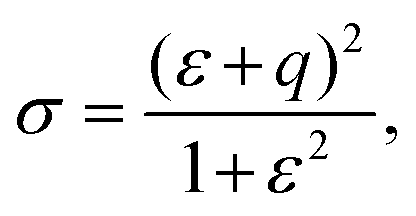
As mentioned above, Fano interaction, after the first discovery in terms of asymmetric spectral line profiles, has been explored in various systems. The quantification of the degree and nature of Fano resonance was analysed using a perturbation-based approach by considering the pre-diagonalized state and thus coupling the discrete bound states with the states having continuum of energies.29 This led to the formula depicting the shape of resonance profile with a scattering cross section given by eqn (1), which is also known as the general Fano profile function:
 | (1) |
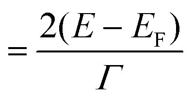 , denotes resonant energy and Γ being the width of autoionized state. The minima and maxima in the Fano profile is given as σmin = 0 (at ε = −q) and σmax = 1 + q2 (at ε = 1/q). The special parameter of utmost importance here is ‘q’, given as the ratio of transition probabilities to the mixed state and to the continuum. The schematic in Fig. 1 depicts the interaction between the discrete and continuum states (Fig. 1a) along with the well separated components of eqn (1) (Fig. 1b), indicating the contribution from discrete state, mixing term and continuum state, to the scattering cross section. In the limit of |q| → ∞, the line shape converges to standard Lorentzian profile of a Breit–Wigner resonance, indicating a weak continuum and a transition through discrete state only. The unit value of Fano parameter, i.e., q = 1, depicts the equal strength of continuum and discrete states, with the maximum and minimum value at Emax = [EF + Γ/(2q)] and Emin = [EF − Γq/2], respectively. The main features of asymmetrical line profile are a maxima accompanied by a minima, also called as antiresonance dip. At q = 0, the asymmetry parameter only describes an asymmetrical dip, also called as antiresonance, and denotes the destructive interference in the system.26,29 Since its first appearance, the Fano formula has been successfully used to reveal the consequential mechanism in the resonant systems including optical cavities,37 photonics,38 nuclear39 and atomic physics40 as well as in molecular systems.41 Some of these mechanisms have been explained in detail in the following sections starting from an example of Fano resonance in the molecular system of pyridine.
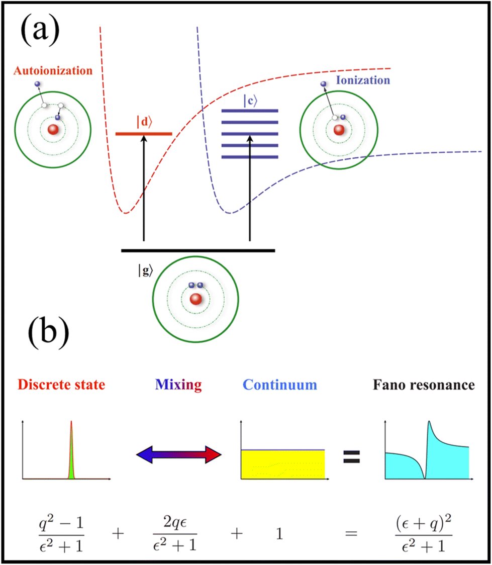 | ||
| Fig. 1 (a) Schematic representation of Fano resonance and (b) a schematic depiction of the Fano formula (eqn (1)) in terms of its components as the interference of discrete states with electronic continuum. Reproduced from ref. 29 with permission from [American Physical Society], copyright [2010]. | ||
2. Fano resonance in molecular systems
Based on the basic formulation by U. Fano, Lombardi et al.,28 modified the expression for excitation profiles, accounting for the interference between molecular orbital energy levels of a molecule and the continuum of conduction band in metals, to generate an asymmetric Fano line-shape from a molecule/metal system to experimentally demonstrate Fano type asymmetry (Fig. 2a). This work was an extension to the theoretical expression of surface enhanced Raman scattering (SERS) to account for the interaction between molecular orbital levels and continuum of states in metal. In this work, the SERS spectrum of CN− comprised of a strong background signal (not due to Rayleigh scattering). Lombardi et al.28 explained that the continuum displayed an electrochemical potential, which is identical to the SERS spectrum of pyridine. Following that, many scientists tried to adequately explain the background followed by the usage of Fano resonance by Lombardi et al., in the context to generate universal theory of SERS, including the contributions from molecular resonance, surface plasmon resonance and charge transfer resonance. The idea of using Fano profiles in SERS-based systems leads to excellent fits of the excitation profiles obtained from SERS (Fig. 2b).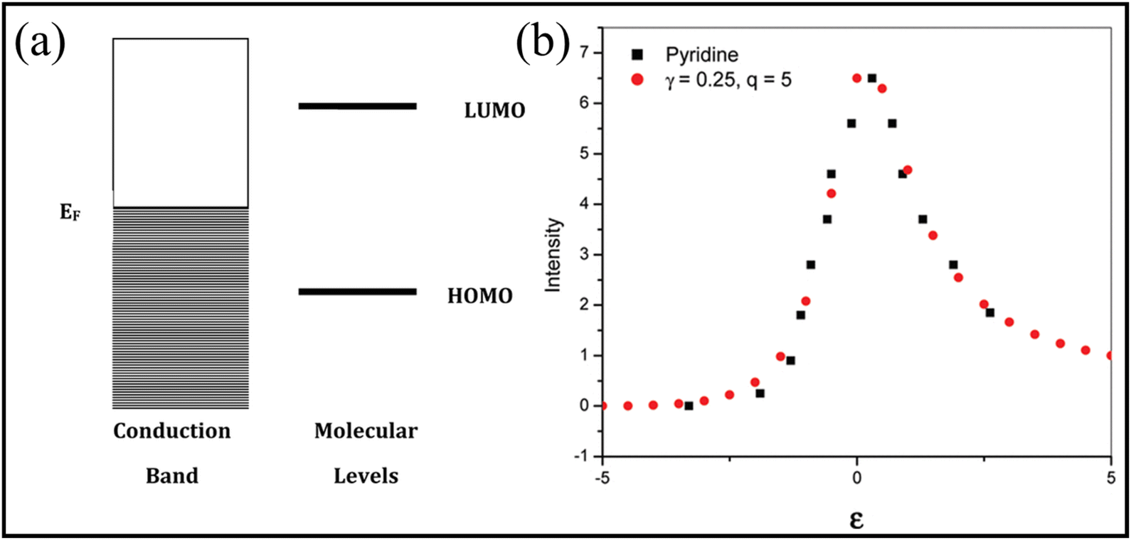 | ||
| Fig. 2 (a) Energy levels of the metal–molecule system. (b) Fano profiles of the voltage-dependent profile of the 1008 cm−1 line of pyridine, wherein red circles represent simulated Raman line shape and black squares represent the experimental data. Reproduced from ref. 28 with permission from [American Chemical Society], copyright [2010]. | ||
In a previous study, the equation consisting of expression for the contribution of three possible sources of resonantly enhanced surface Raman spectra is given as eqn (2) below:28
 | (2) |
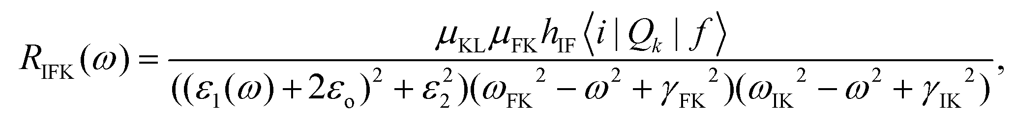
The above eqn (2) is a typical sum over states and is valid when far from any of the resonances. Only a single or a few terms dominate near the resonance. The term in eqn (2), which could be dependent on Fermi energy and depicts charge transfer resonance (ωFK2 − ω2 + γFK2) occurring at ω = ωFK, being the more general type of resonance, has been considered to understand the interaction of the molecule's unfilled, excited level with an unfilled level of the conduction band of the metal. After expanding the term responsible for charge transfer, the final equation comprising the Fano asymmetry parameter is given as eqn (3)
 | (3) |
 .
.
To test this theoretical formulism, the 1008 cm−1 line of the pyridine molecule, previously reported on Ag electrode, in comparison with potential dependence of continuum, was used for fitting with the theoretical Fano line shape. The optimum fit was obtained with a width of 0.25 eV for q = 5. Overall, the modified SERS profile, encompassing the Fano resonance between molecular state and continuum of energy provide by the metal, has been studied as evidence of molecular Fano in these systems (Fig. 2b). This study remains one of the firsts in the area that shows Fano interaction in molecular systems.
2.1 Fano resonance in material systems
Although Fano resonance is explained by its own way of revealing itself in different systems like nanostructures, bulk, metamaterials and photonic systems, Fano resonance in light scattering from material systems42 is predominantly caused by the interaction of electronic continuum provided by the means of heavy doping, electron excitation, etc., with the discrete energy of phonon of a discrete vibration, giving rise to the asymmetrically broadened Raman line shapes having strong Fano profile features, as discussed in detail in section1. For example, in heavily doped p-type Si, the carrier concentration, due to heavy acceptor doping, affects the peak position and FWHM of the Raman line shape of one-phonon Raman spectrum.31 Considering the effects of carrier concentration on the elastic constants of the material, the “static” phonon perturbation is known to split the top of the valence band and eventually change the dispersion relation of the holes. These changes in the band structure causes inter- & intra band redistribution of carriers, which is known to lower the electronic contribution to the free energy of the crystal. Due to this, the energy spent in deforming the crystal is regained through carrier redistribution with a consequent “softening” of the crystal with respect to that vibration. The shift of the peak position towards low energy is a manifestation of the phonon “softening”.15 The energy of continuum of electronic excitations produced by inter-valence-band transitions overlaps with that of the phonon, giving rise to two competing mechanisms: one originating from the continuum of electronic excitations & the other one from one-phonon scattering. The continuum overlaps in energy with the phonon for a broad range of values of carrier concentration because the Si's spin orbit energy is 44 meV, whereas the phonon frequency is 65 meV. Apart from Fano resonance in heavily doped Si,31,43 it has been extensively observed in carbonic materials like graphene,44,45 single walled carbon nanotubes46 and 2-D materials like MoS2![[thin space (1/6-em)]](https://www.rsc.org/images/entities/char_2009.gif) 36 & WS2.47 The mode of electronic continuum is evidently different in each material systems, as discussed in further details in each section.
36 & WS2.47 The mode of electronic continuum is evidently different in each material systems, as discussed in further details in each section.
3. Fano resonance and its wavelength dependence in bulk materials
3.1 Heavily doped c-Si
Heavily doped semiconductors, like Si, prove to be a great platform to observe Fano resonance taking place due to the coupling of continuum of states, occupied by electrons (or holes), to the discrete one-phonon state. For example, in heavily doped p-type Si, the inter-valence-band transitions provide electronic continuum, whose energy then overlaps with the phonon. The one electron excitations are IR-forbidden but Raman-active. The spin–orbit splitting energy is reported to be 44 meV, the electronic continuum overlaps with the phonon energy, which leads to the asymmetric Fano resonance Raman line-shape profiles (Fig. 3). Additionally, the asymmetric line shape also displays a shift in the position phonon energy towards low frequencies owing to the real part of the self-energy due to phonon deformation-potential interaction in the presence of free electrons in the conduction band.31 The above said electron–phonon interaction is dependent on various physical parameters like carrier concentration of dopant atoms, temperature, laser power as well as wavelength of incident laser11 (Fig. 3). Due to the ease of experiment and Raman spectroscopy being one of the versatile tools to probe such processes, degenerately doped Si is considered as one of the best systems to understand Fano resonance in its totality. This establishes that the Fano-Raman line-shape asymmetry and thus the Fano coupling increases with increasing excitation wavelength and increasing doping concentration.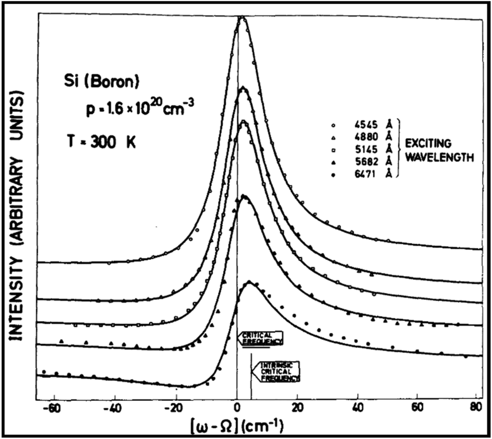 | ||
| Fig. 3 Wavelength-dependent Raman line shape in boron-doped Si (p-type); discrete points show experimental data points and solid lines depict theoretical fits using eqn (1). Reproduced from ref. 48 with permission from [Elsevier], copyright [1973]. | ||
A deeper study by Cerdeira et al.48 analysed the underlying mechanism of wavelength dependence of Fano interaction heavily doped p-type Si. Fig. 3 shows the line shapes for a boron doping of 1.6 × 1020 cm−3 at varying scattering wavelengths. The experimentally obtained curved were fitted with Fano line shape function (eqn (1)). The dependence of Fano parameter “q”, as it is defined as the ratio of scattering probability of the discrete state to that of the continuum, can therefore reveal a wavelength dependence if the two processes have varied frequency dependence. The expression for the leading term near the resonance of the Γ25′ Raman tensor component for electronic scattering (Re) is given by eqn (4).48
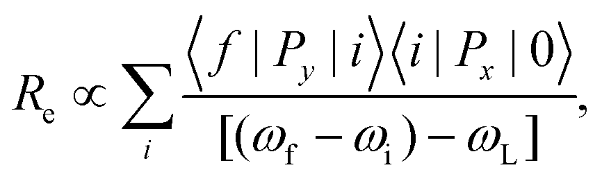 | (4) |
On the other hand, the Raman tensor for one-phonon Raman scattering is given by eqn (5)48
 | (5) |
Approximating the electronic excitation spectrum of Si as one-dimensional critical point E′O at 3.3 eV and E2 at 4.3 eV, the final expression for q comes out as eqn (6).
| q−1 ∝ (ω0 − ωL), | (6) |
Similar observations have been made for heavily doped n-type Si also because of the possible transitions of conduction band valleys between Δ1 and Δ2 conduction bands that are along the 〈100〉 directions. Several reports and consequent theory suggest that there must exist a wavelength-dependent Raman line-shape where Fano resonance is breaking the typical Raman line-shape symmetry, especially in semiconductors.
3.2 Perovskite type oxide (ABO3) systems
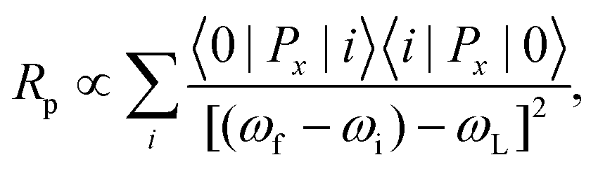
The electron–phonon Fano interaction is not limited to only metal-molecular or extrinsic semiconductor alone; rather, it is a general phenomenon that can be observed in any system where discrete-continuum type interactions are possible. Recently, Kumar et al.49 reported the typical wavelength dependence of orbital-mediated electron–phonon Fano coupling in doped rare-earth orthoferrites. The asymmetric Raman line shape profiles comprising of antiresonance dip has been claimed to carry a wavelength-dependent orbital-mediated lattice rearrangement originating from the electronic excitation from Cr3+(d3)–O2−Fe3+(d5) ions. In this study, the Raman mode at 660 cm−1 has been attributed to this lattice rearrangement. Such an orbital-mediated charge transfer was also explained to be related with antiresonance dip around 600 cm−1 (Fig. 4). Comparison between the resonant Raman spectra recorded using 785 nm and 633 nm laser, closer to the charge transfer gap of Cr3+(d3) and Fe3+(d5) ions, also showed significant wavelength dependence. Typically, Fano resonance is not observed in traditional semiconductors due to the considerably higher energy scale associated with interband electronic transitions compared to phonon excitations in these materials. Nevertheless, the introduction of dopants allows for the creation of a continuum of electronic energy states, causing a shift in the Fermi level toward the valence band/conduction band. The electrons at the Fermi level become nearly unrestricted in their ability to interact with phonons. In this study, a 50% substitution of Cr in RFeO3 samples was undertaken with the anticipation of inducing Fano resonance scattering. To delve into this phenomenon, resonant Raman scattering data were gathered using lasers at 785 and 633 nm. | ||
| Fig. 4 Raman spectra for Cr-doped EuFeO3 samples using excitation wavelengths (a) 785 nm and (b) 633 nm at different laser powers. Reproduced from ref. 49 with permission from [American Chemical Society], copyright [2022]. | ||
The choice of a 633 nm wavelength (approximately 1.95 eV) closely aligns with the charge transfer (CT) gap (∼2 eV) involving Cr3+(d3) and Fe3+(d5) ions. Consequently, the absorption is maximized for the 633 nm wavelength, suggesting a minimized penetration depth for lower excitation wavelength. This aligns with the observation that the Raman modes of the Pnma space group exhibit greater intensity at 785 nm than at 633 nm. Fig. 1 highlights significant alterations in the antiresonance dip concerning both the excitation laser wavelength and incident power. The origin of this dip is explicable in terms of the interaction between the electronic continuum of electronic excitations and discrete phonon lines. The pronounced reliance of the Raman line shape on the excitation wavelength arises from the fundamentally distinct behaviours exhibited by these two scattering processes. This study reaffirms the wavelength dependence of the Fano-Raman line-shape.
4. Excitation wavelength-dependent Fano interaction in nanostructures
From the discussion above, there is no apparent fundamental restriction on the materials’ dimensions for Fano resonance with its parametric identifiers like wavelength dependence to be observed if the basic condition of discrete/continuum overlap is met. This is evident from various reports about the presence of Fano interaction in nanomaterials; however, these reports do not clearly comment on its wavelength dependence. As a consequence, no theoretical framework has been developed to be experimentally validated. Following are some low dimensional systems where Fano effects and its wavelength dependence have been reported.4.1 Silicon nanocrystals
In a recent study, Sagar et al.50 reported the role of excitation wavelength on asymmetric Raman line-shape in a colloidal Si nanocrystal system. In a successful attempt to study phonon confinement from Si, the origin of asymmetry in 5.3 nm sized nanocrystals was studied as a function of excitation wavelength. In a striking observation, in this measurement, a reversed trend of Fano resonance with the excitation energies as opposed to the bulk Si was observed, i.e., the line width and Fano interaction both decrease as the excitation wavelength decreases (Fig. 5a–c). Such an atypical wavelength dependent Fano-Raman line-shape was explained to be caused likely by shift in the energy electronic continuum with the change in excitation wavelength and size of the NS. A representative schematic (Fig. 5d) shows the proposed scenarios, i.e., the modification of continuous density of states, thus giving rise to mini gaps and narrow band like levels due to quantum confinement, suggesting that due to the inter-band photoexcitation of electron–hole pairs, a dissimilarity in the band structures of electron and holes causes asymmetric excitonic wavefunction. In this qualitative model (Fig. 5d), the strong quantum confinement present in smaller nanocrystals results in the formation of band-like levels, which can host a continuum of photoexcited electrons. The level spacing (Δ) approaches the longitudinal optical (LO) phonon energy, leading to the coupling of LO phonons to the continuum, resulting in the observed strong Fano-line shapes. Conversely, in larger nanocrystals, the level spacing is smaller than the LO phonon energy, leading to limited interaction between the LO phonon and electrons and resulting in a nearly symmetric Lorentzian line-shape. Though the report by Sagar50et al. shows (atypical non-Fano type) wavelength-dependent Fano-Raman line-shape, the explanation remains qualitative in nature and is not a representative of a true Fano type energy dispersive line-shape.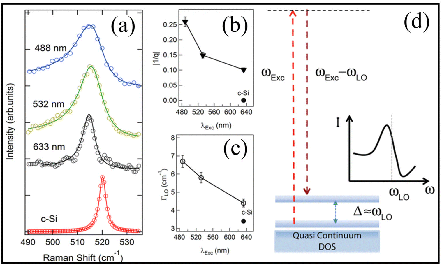 | ||
| Fig. 5 (a) Excitation wavelength-dependent Raman spectra of the LO mode for the 5.3 nm (EPL = 1.29 eV) sample with the Raman spectrum for bulk intrinsic c-Si shown for comparison and collected on the same setup as nanocrystalline samples. (b and c) Variation of the asymmetry factor and line width as a function of excitation wavelength. (d) A qualitative picture describing the proposed model that can explain observed size-dependent Fano interference. Reproduced from ref. 50 with permission from [American Chemical Society], copyright [2015]. | ||
4.2 Single walled carbon nanotube
Like bulk semiconductors, Raman spectroscopy of single walled carbon nanotube (SWCNT) has proved to be extremely significant and a non-destructive characterization tool to understand the electronic and vibrational properties. Zhang et al.51 observed the Raman mode in the range of 1650–2000 cm−1 for small diameter SWCNT (Fig. 6). The Raman spectra from semiconducting and metallic tube display excitation wavelength-dependent line-shape. The assignment of the tubes (n,m) has been done on the basis of their radial breathing mode frequencies and intensities at various excitation energy, along the Kataura plot reported by Son et al.52 The intensity of the M band and 1950 cm−1 band, which is a combination of in plane transverse optical and longitudinal acoustic phonon (iTOLA), does not change with excitation wavelength, related to the G band. As the excitation wavelength decreases, a shoulder develops at the high-energy side of the iTOLA band (Fig. 6). Similar to the abovementioned report for Si NSs, a wavelength dependence, in contrast to the case of Fano type, is also observed from individual tubes when 594, 543 and 514 nm excitations were used. The observation of some unusual single-tube Raman spectra featuring enhanced second-order modes was attributed to the resonant scattering of photons with exciton transitions within the nanotubes. No attempt to develop a consolidate model on Fano-type wavelength-dependent Raman line-shape variation was made, leaving the atypical wavelength dependence unresolved. It is important here to mention that low-dimensional carbon is one of the systems where Fano interactions have been reported with no explanation of the wavelength dependence.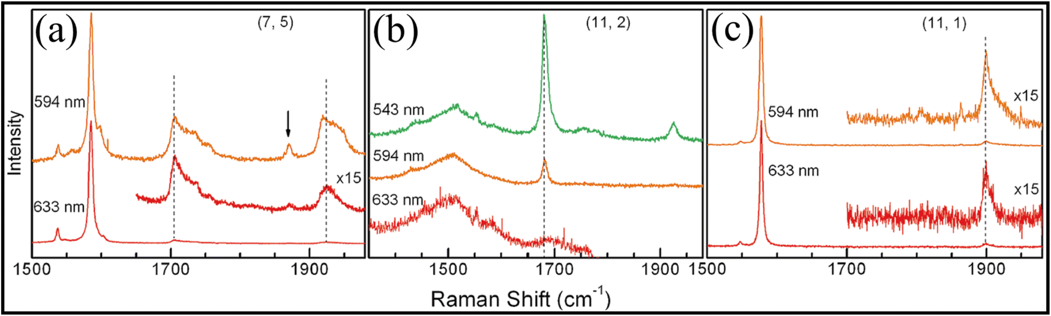 | ||
| Fig. 6 Excitation wavelength-dependent Raman spectra of three individual tubes: (a) semiconducting tube (7, 5), (b) metallic tube (11, 2), and (c) semiconducting tube (11,1). Spectra were acquired using laser wavelengths of 633, 594, and 543 nm. Arrow in panel a indicates the weak G + RBM combination feature. All spectra are normalized to the G band peak of each tube. Reproduced from ref. 51 with permission from [American Chemical Society], copyright [2009]. | ||
5. 2D materials
5.1 Graphene
The ability of carbon-based 2-D materials, like graphene, to revolutionize next-gen electronics and photonics have fuelled researchers to analyse various subtle interactions and physical properties in these materials.45 Raman spectroscopy has been utilized as a non-destructive tool to probe graphene layers vis-à-vis understanding the electron–phonon interaction and interlayer interactions. Tan et al.,45 analysed the interlayer shear mode, i.e., low-energy E2g mode denoted as the vibration of the C peak of few layer graphene (FLG), ranging from bilayer graphene (BLG) to bulk graphite. They used three BragGrate notch filters (BNF) in combination with a single monochromator (Fig. 7a) to probe Raman modes with vibrational wavenumber as low as ∼10 cm−1, leading to good Raman signals with shorter acquisition times. The authors in this study used low doped Si with resistivity ≥2000 Ω cm and suspended the FLG ON 2–5 μm holes (Fig. 7b). Fig. 7c shows the Stokes and anti-Stokes Raman spectra of the supported and suspended BLG, 11LG and bulk graphite, where NLG denotes FLG with N layers. Fig. 7d shows the layer dependence of Raman spectra, and Fig. 7e plots the peak position of G and C peak as a function of 1/N, where N is the number layer. It can be clearly seen that the position of G peak remains constant at ∼1581 cm−1, whereas the C peak shifts towards higher wavenumber side as N increases.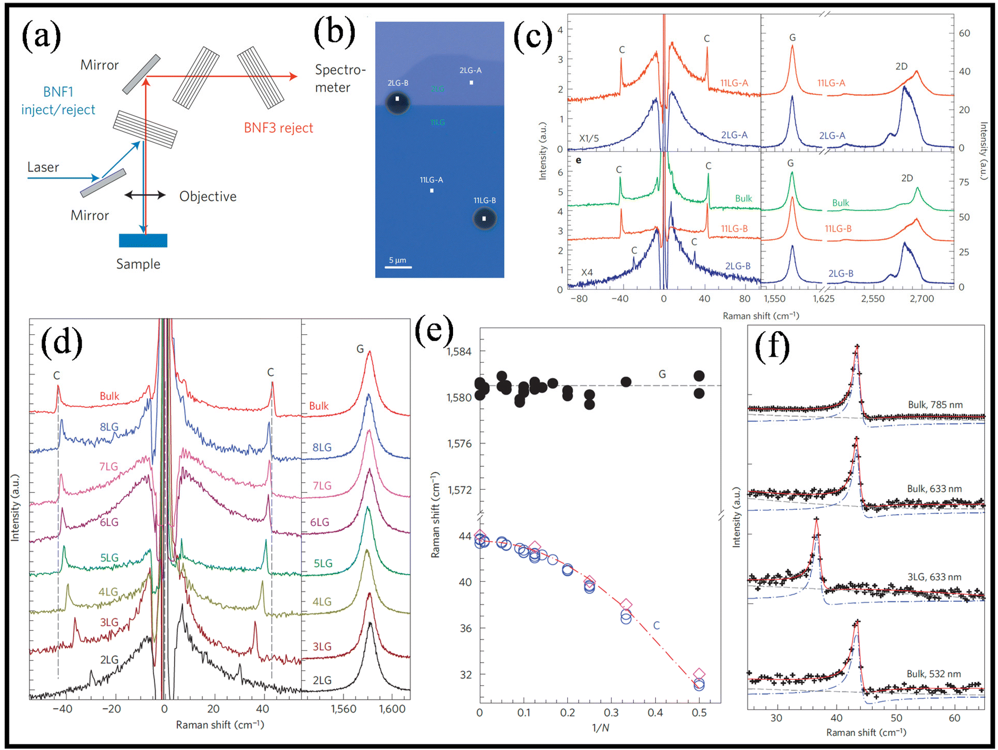 | ||
| Fig. 7 (a) Schematic diagram of our single monochromator with three BragGrate notch filters (BNF). (b) Optical micrography of the FLG sample. 2LG-A/11LG-A and 2LG-B/11LG-B denote supported and suspended flakes, respectively, (c) S/AS spectra of supported flakes and suspended flakes, top and bottom, respectively, in the C peak region (left) and S spectra in the G/2D peaks region (right), (d) S/AS Raman spectra for the C peak spectral region (left) and S Raman spectra for the G peak spectral region (right). (e) Peak positions Pos(G) (filled black circles) and Pos(C) (open blue circles) as a function of inverse layer number, (f) C peaks with BWF fit for bulk graphite and 3LG. Fitted curve (solid red lines); background (dashed lines); BWF component (dash–dotted lines). Reproduced from ref. 45 with permission from [Springer Nature], copyright [2012]. | ||
The ratio of the intensity of C and G peak, denoted as I(C)/I(G), at 633 nm was determined after calibration to consider the distinct response of the system in the C and G peak spectral regions. The calculated values are approximately 0.0052, 0.044, and 0.049. Additionally, the ratio of the integrated peak areas, A(C)/A(G), is approximately 0.00038, 0.0023, and 0.0034 for bilayer graphene (BLG), 11-layer graphene (11LG), and bulk graphite, respectively. These ratios exhibit slight variations with excitation energy. For instance, at 532 nm, the ratio I(C)/I(G) is approximately 0.025, and A(C)/A(G) is approximately 0.00096 for bulk graphite. The dependence of these ratios on the electron–phonon coupling (EPC) suggests that EPC(C) is significantly smaller than EPC(G). The dependence of Pos(C) on the number of layers is explicable through the consideration of a linear-chain model, suggesting implications for Bernal-stacked few-layer graphene (FLG).
In this context, the observed hardening of the C mode is attributed not to variations in interlayer coupling but rather to an overall increase in the restoring force. This increase is linked to the differing binding strengths of surface layers compared to those in the bulk, as observed in the transition from bilayer graphene (BLG) to bulk graphite. For a given number of layers (N), the variations in Pos(C) are anticipated when interlayer coupling is modified, such as through alterations in spacing or relative layer orientation. In the latter case, the expectation is also for mode splitting to occur. The findings are substantiated by additional support from ab initio calculations conducted through density functional theory (DFT) and Density Functional Perturbation Theory (DFPT).
The wavelength-dependent change in the peak position and FWHM of C peak was analysed using three different excitation wavelengths (532, 633 &785 nm). The C peak, corresponding to the E2g mode at position x, exhibits non-dispersive behaviour with excitation energy, in contrast to the D, D′, and D′′ peaks along with their overtones. This lack of dispersion is evidenced in Fig. 7f, where the C peak remains unchanged for excitation wavelengths of 785, 633, and 532 nm. The full width at half maximum (FWHM) of the C peak (FWHM(C)) is influenced by two main factors governing the linewidth of E2g Raman modes in graphene and graphite: the electron–phonon coupling (EPC) term and anharmonic phonon–phonon interactions.
In undoped conditions, FWHM(G) is approximately 12–14 cm−1 in single-layer graphene (SLG) and bulk graphite, predominantly due to the dominant EPC contribution. The phonon–phonon contribution is about ∼1.7 cm−1. Notably, the experimental FWHM© is significantly smaller compared not only to the overall FWHM(G) but also in relation to the non-EPC component of FWHM(G). This discrepancy suggested a considerably smaller electron–phonon coupling for C (EPC(C)) compared to G (EPC(G)), in line with the lower intensity of the C peak.
5.2 Tungsten disulphide (WS2)
The 2-D materials with stoichiometry of MX2 (M = Mo, W; X = S, Se, Te) provides the researcher with an opportunity to understand electron phonon coupling and the interplay of quantum confinement & dielectric screening in these systems. In the realm of their optical transitions and light–matter interaction, a robust exciton feature guides them, characterized by binding energies in the order of several hundred meV. Governed by intense spin–orbit (SO) coupling and exciton–phonon interaction, the system facilitates the exploration, dark excitons, phonon-assisted excitonic luminescence up conversion, exciton–phonon scattering, etc. In an attempt to understand one of the 2D materials, namely, WS2, the Raman scattering analysis of the excitonic resonant Raman scattering (RRS) spectra of few-layer WS2 was presented by Tan47et al. The material was excited by 11 laser lines that covered all A, B, and C exciton transition energies at different sample temperatures ranging from 4 to 300 K.Fig. 8a & b shows the ultra-low frequency RRS of the WS2 layers. Comprising three atomic layers, with one W layer sandwiched between two S layers, each layer is referred to as a trilayer (TL). The resonance of excitation energy with the C excitation transition is in the range of 2.81 to 2.54 eV; the only observable modes are interlayer shear modes (SMs) and interlayer breathing modes (LBMs), having a strict frequency dependence on the number of layers in WS2. On the other hand, when the excitation energy is resonant with B exciton (2.41 to 2.18 eV), two new peaks located at 27.8 & 45.4 cm−1 were observed, having no frequency and layer number dependence and were labelled as acoustic phonons (TA & LA, respectively), with finite wave vector k. In between the energy range of A and B excitons, the LA and TA peaks vanished.
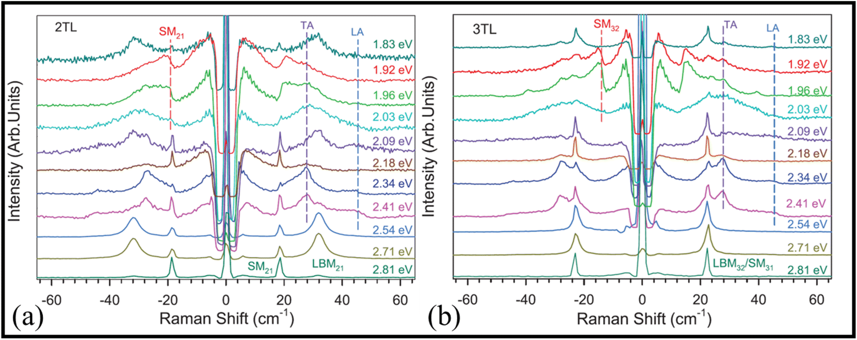 | ||
| Fig. 8 (a) Ultra-low frequency Raman spectra of 2TL and (b) 3TL WS2 samples with different laser excitation energy (EL). Reproduced from ref. 47 with permission from [IOP Publishing], copyright [2014]. | ||
Lastly, the authors observed that when the laser excitation energy was close to A exciton (1.92 and 1.96 eV), a new peak with asymmetric Fano line shape was originated. The authors proposed and validated the origin of such Fano line shape from the interference between the SMNN−1 discrete phonons and continuum of excitonic states at resonant Raman frequency using theoretical Fano function. Overall, in this study, several forbidden phonon modes were analysed using a range of excitation wavelengths. By fitting the experimentally obtained Fano Raman line shaped from SM and LA modes with the help of parity selection rules of Raman scattering, the authors successfully determined the bright-dark fine structure of 1s A exciton, hence probing the exciton–phonon interaction in WS2.
In another interesting study from the same author,53 Fano resonance and its wavelength dependence between the dark excitons and zone-edged acoustic phonons in few layer WS2 were reported. There results of resonant interaction between discrete phonons with large momentum at the M-point of the Brillouin zone and the continuum of dark excitonic states were analysed using Fano asymmetry parameter q.
5.3 Molybdenum di-sulphide (MoS2)
With the advent of better detectors and efficient lasers, Raman spectroscopy has proved to be the best technique to understand the vibrational properties of 2D materials in their macroscopic as well as monolayered forms.54–58 Raman spectroscopy has revealed a great deal of information in terms of analysing the physical perturbation and subtle scale phenomena. The usage of Raman microscopy is not limited to the identification of number of layers/thicknesses of 2-D material but rather extends into the studies of intriguing light–matter interactions. The strong physical and chemical perturbations like quantum confinement and electron–phonon interaction have been explored for a better usage in devices due to their direct effect on the transport and optical properties of these materials. Amongst these perturbations, a study by Tanwar et al.36 reported Fano-type wavelength-dependent Raman line-shape variation in MoS2. The two characteristic vibrational modes of MoS2, namely, E12g and A1g, were explored for their Fano type interaction with the continuum present in the system. A parametric Raman line shape analysis was presented in order to analyse the origin of asymmetry induced in the experimental The Raman line shape was obtained from shining two different excitation wavelengths on the material. The asymmetry in the Raman line shape was assigned to the electron–phonon interaction having an excitation wavelength dependence (Fig. 9). The origin of electronic continuum was substantiated by the broad photoluminescence (PL) emission due to the energy difference between A and B excitonic levels, leading to exciton-mediated Fano-like interference in bulk MoS2. The work by Tanwar et al. remains one of the few reports where true Fano-type wavelength-dependent Fano-Raman line-shapes were demonstrated. It is important here to mention that this work too lacks the theoretical rationale that can confirm the energy dispersive behaviour of Fano interaction in low dimensional materials. Apparently, little work has been done towards establishing the nature of wavelength-dependent Fano interaction in nanostructures due to which the area remains unexplored, and a lot of scientific mystery is waiting to be unearthed.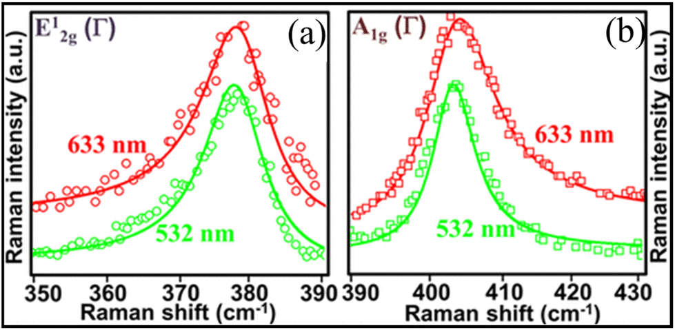 | ||
| Fig. 9 Theoretical fitting (solid lines) of experimentally observed Raman spectra (discrete points) of MoS2 nano-flakes corresponding to the E12g mode (a) and A1g mode (b) recorded using 633 and 532 nm laser excitation represented in red and green colours, respectively. Reproduced from ref. 36 with permission from [American Chemical Society], copyright [2022]. | ||
6. Fano resonance in metamaterials and photonic systems
Metamaterials are found to be consisting of periodic structures of subwavelength size, which can be tailored to support a resonant response to applied electromagnetic wave.59,60 The excitation of bright and dark modes by the incident light, due to symmetry breaking, leads to Fano resonance. The optimization of Fano line shape in such a system is done by changing the structural symmetry of the resonator to give a sharp spectral response (Q factor). But such an optimisation has its own limitations and can lead to low resonance intensities as well as limiting the figure of merit (FoM) by coupling the plasmonic resonance to the first order lattice mode (FOLM). In a study by Tan59et al., the coupling of an asymmetric split ring resonator (ASRR) to the FOLM of the resonator array was experimentally analysed. They observed an enhancement of both Q factor and FoM. In a typical ASSR, the excited split mode consists of low frequency Fano resonance and high frequency dipole resonance. The low frequency Fano resonance of the split mode implies a large period to couple with the lattice mode, which can be inefficient. Therefore, the capacitive coupling of ASSR was changed to inductive by flipping the arms of ASSR (inset Fig. 10). The higher (Fig. 10a) or lower (Fig. 10b) resonant frequency is then decided by the nature of coupling between the resonator arms. | ||
| Fig. 10 Fano resonances of different aluminium resonator configurations. (a) Square configuration of end-coupled resonator arms and (b) side-coupled configuration with the resonating arms flipped. Reproduced from ref. 59 with permission from [John Wiley and Sons], copyright [2020]. | ||
In summary, a terahertz asymmetric resonator with a Fano resonance as the higher frequency split mode was used to perform lattice mode matching. This study demonstrated a general method for Q factor enhancement in metamaterial resonances for these to be utilized in various applications such as lasing spacers and sensing. Fano resonance in metamaterials and photonic system has been rigorously studied to develop metamaterial devices for real world applications.61–64
7. Summary and future outlook
Even after the advent of nanoscience & nanotechnology, the grey area of size-modulated Raman excitations in nanomaterials has been least discussed in the last few decades due to the predominance of nanotechnology over nanoscience. Overall, the current review illuminates the understanding of the role of size in excitation wavelength-dependent electron–phonon interaction and thereby drawing the attention of researchers working in this field to resolve the role of dominant players that causes inhomogeneity in nanomaterials. Also, a better understanding of electron–phonon interaction by analysing the role of lesser studied yet critical perturbation, i.e., excitation laser frequency, will certainly help the scientific community to contemplate upon this key parameter for broadened the understanding of various mechanisms taking place at the nanoscale. Some possible futuristic analysis could be as follows.Developing an exhaustive theoretical framework to understand and incorporate the role of latent players, for example, the modified electronic continuum in nanomaterials needs a theoretical modelling in the form of a modified Fano equation.
As mentioned above, the inhomogeneity and size-dependent variation in excitation wavelength penetration depth appears to be hindering the true Fano type behaviour in nanomaterials. This can be validated only after developing an appropriate theoretical framework.
There are hidden variables that govern the dynamics of physical perturbation and processes in nanomaterials’ domain; therefore, the theory needs to be established, which can be validated through designing neat experiments so that the true wavelength-dependent Fano resonance in such type of systems can be established.
Conflicts of interest
Authors declare no conflicts of interest.Acknowledgements
Authors acknowledges financial support from Science and Engineering Research Board, Govt. of India (grant no. CRG/2022/002787). Authors are thankful to Er. Nitin Upadhyay and Prashant Gupta for technical support. One of the authors (M. T.) acknowledges acknowledge IIT Indore & DST (file DST/INSPIRE/03/2018/000910/IF180398) and Government of India, for providing fellowships. Facilities received from Department of Science and Technology (DST), Govt. of India, under FIST scheme (grant number SR/FST/PSI-225/2016) is highly acknowledged. Help from Dr Chanchal Rani, Dr Suchita Kandpal, Dr Tanushree Ghosh & Mr Love Bansal is also acknowledged. Authors thank all their teachers and Mr Rajesh Kumar (Learning Resource Centre, IIT Indore) for various resources.References
- L. Gu, D. J. Hall, Z. Qin, E. Anglin, J. Joo, D. J. Mooney, S. B. Howell and M. J. Sailor, Nat. Commun., 2013, 4, 2326 CrossRef.
- M.-H. Sun, S.-Z. Huang, L.-H. Chen, Y. Li, X.-Y. Yang, Z.-Y. Yuan and B.-L. Su, Chem. Soc. Rev., 2016, 45, 3479–3563 RSC.
- H. Imahori and T. Umeyama, J. Phys. Chem. C, 2009, 113, 9029–9039 CrossRef CAS.
- J. Qiao, Y. Liu, F. Hong and J. Zhang, Chem. Soc. Rev., 2013, 43, 631–675 RSC.
- M. Tanwar, D. K. Pathak, A. Chaudhary, P. Yogi, S. K. Saxena and R. Kumar, J. Phys. Chem. C, 2020, 124, 6467–6471 CrossRef CAS.
- C. M. Hessel, J. Wei, D. Reid, H. Fujii, M. C. Downer and B. A. Korgel, Raman Spectroscopy of Oxide-Embedded and Ligand-Stabilized Silicon Nanocrystals, https://pubs.acs.org/doi/abs/10.1021/jz300309n, (accessed June 10, 2018).
- E. G. Barbagiovanni, D. J. Lockwood, P. J. Simpson and L. V. Goncharova, Appl. Phys. Rev., 2014, 1, 011302 Search PubMed.
- S. K. Saxena, P. Yogi, S. Mishra, H. M. Rai, V. Mishra, M. K. Warshi, S. Roy, P. Mondal, P. R. Sagdeo and R. Kumar, Phys. Chem. Chem. Phys., 2017, 19, 31788–31795 RSC.
- M. Tanwar, D. K. Pathak, A. Chaudhary, S. K. Saxena and R. Kumar, J. Phys. Chem. C, 2020, 124, 16675–16679 CrossRef CAS.
- A. N. Thiessen, M. Ha, R. W. Hooper, H. Yu, A. O. Oliynyk, J. G. C. Veinot and V. K. Michaelis, Chem. Mater., 2019, 31, 678–688 Search PubMed.
- F. Cerdeira, T. A. Fjeldly and M. Cardona, Phys. Rev. B: Solid State, 1974, 9, 4344–4350 Search PubMed.
- M. Tanwar, D. K. Pathak, A. Chaudhary, A. S. Krylov, H. Pfnür, A. Sharma, B. Ahn, S. Lee and R. Kumar, J. Phys. Chem. Lett., 2021, 12, 2044–2051 CrossRef CAS PubMed.
- C. Rani, M. Tanwar, T. Ghosh, S. Kandpal, D. K. Pathak, A. Chaudhary, P. Yogi, S. K. Saxena and R. Kumar, Anal. Chem., 2022, 94, 1510–1514 Search PubMed.
- P. Yogi, M. Tanwar, S. K. Saxena, S. Mishra, D. K. Pathak, A. Chaudhary, P. R. Sagdeo and R. Kumar, Anal. Chem., 2018, 90, 8123–8129 CrossRef CAS PubMed.
- B. G. Burke, J. Chan, K. A. Williams, Z. Wu, A. A. Puretzky and D. B. Geohegan, J. Raman Spectrosc., 2010, 41, 1759–1764 CrossRef.
- S. K. Saxena, R. Borah, V. Kumar, H. M. Rai, R. Late, V. G. Sathe, A. Kumar, P. R. Sagdeo and R. Kumar, J. Raman Spectrosc., 2016, 47, 283–288 CrossRef CAS.
- R. Kumar, G. Sahu, S. K. Saxena, H. M. Rai and P. R. Sagdeo, Silicon, 2014, 6, 117–121 Search PubMed.
- M. Tanwar, S. K. Saxena and R. Kumar, J. Phys. Chem. C, 2022, 126, 4733–4743 CrossRef CAS.
- M. Tanwar, D. K. Pathak, C. Rani, S. Kandpal, T. Ghosh, P. Mondal, A. Chaudhary and R. Kumar, J. Phys. Chem. C, 2021, 125, 12767–12773 Search PubMed.
- E. H. Hasdeo, A. R. T. Nugraha, M. S. Dresselhaus and R. Saito, Phys. Rev. B: Condens. Matter Mater. Phys., 2014, 90, 245140 CrossRef.
- C. Rani, M. Tanwar, S. Kandpal, T. Ghosh, L. Bansal and R. Kumar, J. Phys. Chem. Lett., 2022, 13, 5232–5239 CrossRef CAS PubMed.
- N. Caselli, F. Intonti, F. La China, F. Biccari, F. Riboli, A. Gerardino, L. Li, E. H. Linfield, F. Pagliano, A. Fiore and M. Gurioli, Nat. Commun., 2018, 9, 396 CrossRef PubMed.
- R. W. Boyd and D. J. Gauthier, Nature, 2006, 441, 701–702 Search PubMed.
- W. Zhu, Y. Fan, C. Li, R. Yang, S. Yan, Q. Fu, F. Zhang, C. Gu and J. Li, Nanoscale, 2020, 12, 8758–8767 Search PubMed.
- M. F. Limonov, M. V. Rybin, A. N. Poddubny and Y. S. Kivshar, Nat. Photonics, 2017, 11, 543–554 CrossRef CAS.
- U. Fano, Phys. Rev., 1961, 124, 1866–1878 CrossRef CAS.
- C. Rani, S. Kandpal, T. Ghosh, L. Bansal, M. Tanwar and R. Kumar, Phys. Chem. Chem. Phys., 2023, 25, 1627–1631 RSC.
- J. R. Lombardi and R. L. Birke, J. Phys. Chem. C, 2010, 114, 7812–7815 CrossRef CAS.
- A. E. Miroshnichenko, S. Flach and Y. S. Kivshar, Rev. Mod. Phys., 2010, 82, 2257–2298 CrossRef CAS.
- M. F. Limonov, Adv. Opt. Photonics, 2021, 13, 703–771 CrossRef.
- F. Cerdeira, T. A. Fjeldly and M. Cardona, Phys. Rev. B: Solid State, 1973, 8, 4734–4745 CrossRef CAS.
- M. Chandrasekhar, J. B. Renucci and M. Cardona, Phys. Rev. B: Solid State, 1978, 17, 1623–1633 CrossRef CAS.
- K. P. Jain, A. K. Shukla, S. C. Abbi and M. Balkanski, Phys. Rev. B: Condens. Matter Mater. Phys., 1985, 32, 5464–5467 CrossRef CAS PubMed.
- R. Kumar and M. Tanwar, J. Raman Spectrosc., 2021, 52, 2100–2118 CrossRef CAS.
- P. Yogi, S. Mishra, S. K. Saxena, V. Kumar and R. Kumar, J. Phys. Chem. Lett., 2016, 7, 5291–5296 CrossRef CAS PubMed.
- M. Tanwar, L. Bansal, C. Rani, S. Rani, S. Kandpal, T. Ghosh, D. K. Pathak, I. Sameera, R. Bhatia and R. Kumar, ACS Phys. Chem. Au, 2022, 2, 417–422 CrossRef CAS PubMed.
- H. S. Eisenberg, Y. Silberberg, R. Morandotti, A. R. Boyd and J. S. Aitchison, Phys. Rev. Lett., 1998, 81, 3383–3386 CrossRef CAS.
- E. Ozbay, Science, 2006, 311, 189–193 CrossRef CAS PubMed.
- A. Pálffy, Z. Harman and W. Scheid, Phys. Rev. A, 2007, 75, 012709 CrossRef.
- U. Fano and J. W. Cooper, Rev. Mod. Phys., 1968, 40, 441–507 CrossRef CAS.
- J. Fransson and A. V. Balatsky, Phys. Rev. B: Condens. Matter Mater. Phys., 2007, 75, 153309 CrossRef.
- D. Yoon, D. Jeong, H.-J. Lee, R. Saito, Y.-W. Son, H. C. Lee and H. Cheong, Carbon, 2013, 61, 373–378 CrossRef CAS.
- M. Jouanne, R. Beserman, I. Ipatova and A. Subashiev, Solid State Commun., 1975, 16, 1047–1049 CrossRef CAS.
- A. Castellanos-Gomez, G. Rubio-Bollinger, S. Barja, M. Garnica, A. L. Vázquez de Parga, R. Miranda and N. Agraït, Appl. Phys. Lett., 2013, 102, 063114 Search PubMed.
- P. H. Tan, W. P. Han, W. J. Zhao, Z. H. Wu, K. Chang, H. Wang, Y. F. Wang, N. Bonini, N. Marzari, N. Pugno, G. Savini, A. Lombardo and A. C. Ferrari, Nat. Mater., 2012, 11, 294–300 Search PubMed.
- S. D. M. Brown, A. Jorio, P. Corio, M. S. Dresselhaus, G. Dresselhaus, R. Saito and K. Kneipp, Phys. Rev. B: Condens. Matter Mater. Phys., 2001, 63, 155414 CrossRef.
- Q.-H. Tan, Y.-J. Sun, X.-L. Liu, Y. Zhao, Q. Xiong, P.-H. Tan and J. Zhang, 2D Mater., 2017, 4, 031007 CrossRef.
- F. Cerdeira, T. A. Fjeldly and M. Cardona, Solid State Commun., 1973, 13, 325–328 CrossRef CAS.
- A. Kumar, O. V. Rambadey, H. Rai and P. R. Sagdeo, J. Phys. Chem. C, 2022, 126, 5403–5410 CrossRef CAS.
- D. M. Sagar, J. M. Atkin, P. K. B. Palomaki, N. R. Neale, J. L. Blackburn, J. C. Johnson, A. J. Nozik, M. B. Raschke and M. C. Beard, Nano Lett., 2015, 15, 1511–1516 CrossRef CAS PubMed.
- L. Zhang, L. Huang, M. Lind, V. Liao, S. O'Brien and Z. Yu, J. Phys. Chem. C, 2009, 113, 16432–16438 CrossRef CAS.
- H. Son, A. Reina, Ge. G. Samsonidze, R. Saito, A. Jorio, M. S. Dresselhaus and J. Kong, Phys. Rev. B: Condens. Matter Mater. Phys., 2006, 74, 073406 CrossRef.
- Q.-H. Tan, Y.-M. Li, J.-M. Lai, Y.-J. Sun, Z. Zhang, F. Song, C. Robert, X. Marie, W. Gao, P.-H. Tan and J. Zhang, Nat. Commun., 2023, 14, 88 CrossRef CAS PubMed.
- D. P. Khatua, A. Singh, S. Gurung, M. Tanwar, R. Kumar and J. Jayabalan, Opt. Mater., 2022, 126, 112224 CrossRef CAS.
- S. Kandpal, T. Ghosh, C. Rani, M. Tanwar, M. Sharma, S. Rani, D. K. Pathak, R. Bhatia, I. Sameera, J. Jayabalan and R. Kumar, ACS Mater. Au, 2022, 2, 293–300 CrossRef CAS PubMed.
- D. P. Khatua, A. Singh, S. Gurung, S. Khan, M. Tanwar, R. Kumar and J. Jayabalan, J. Phys.: Condens. Matter, 2022, 34, 155401 CrossRef CAS PubMed.
- S. Kandpal, T. Ghosh, C. Rani, S. Rani, D. K. Pathak, M. Tanwar, R. Bhatia, I. Sameera and R. Kumar, Sol. Energy Mater. Sol. Cells, 2022, 236, 111502 CrossRef CAS.
- S. Rani, M. Tanwar, M. Sharma, L. Bansal, R. Kumar, R. Bhatia and S. Ivaturi, J. Energy Storage, 2023, 58, 106343 CrossRef.
- T. C. W. Tan, E. Plum and R. Singh, Adv. Opt. Mater., 2020, 8, 1901572 CrossRef CAS.
- B. Wang, P. Yu, W. Wang, X. Zhang, H.-C. Kuo, H. Xu and Z. M. Wang, Adv. Opt. Mater., 2021, 9, 2001520 CrossRef CAS.
- C. Rani, M. Tanwar, T. Ghosh, S. Kandpal, S. K. Saxena and R. Kumar, Phys. Rep., 2023, 1037, 1–41 CrossRef.
- T. Lee, J. Jang, H. Jeong and J. Rho, Nano Convergence, 2018, 5, 1 CrossRef CAS PubMed.
- W. X. Lim, M. Manjappa, P. Pitchappa and R. Singh, Adv. Opt. Mater., 2018, 6, 1800502 CrossRef.
- C. Rani and R. Kumar, Chem. Commun., 2024, 60, 2115–2124 RSC.
| This journal is © The Royal Society of Chemistry 2024 |