
Insights into synaptic functionality and resistive switching in lead iodide flexible memristor devices†
Muskan
Jain
ab,
Mayur Jagdishbhai
Patel
c,
Lingli
Liu
 d,
Jeny
Gosai
be,
Manish
Khemnani
ab,
Himangshu Jyoti
Gogoi
f,
Mun Yin
Chee
d,
Antonio
Guerrero
g,
Wen Siang
Lew
d and
Ankur
Solanki
*ab
d,
Jeny
Gosai
be,
Manish
Khemnani
ab,
Himangshu Jyoti
Gogoi
f,
Mun Yin
Chee
d,
Antonio
Guerrero
g,
Wen Siang
Lew
d and
Ankur
Solanki
*ab
aDepartment of Physics, School of Energy Technology, Pandit Deendayal Energy University, Raysan, Gandhinagar 382426, India. E-mail: ankur.solanki@sot.pdpu.ac.in
bFlextronics Lab, Pandit Deendayal Energy University, Gandhinagar, Gujarat 382426, India
cDepartment of Chemistry, Indian Institute of Technology Guwahati, Guwahati 781039, Assam, India
dSchool of Physical and Mathematical Sciences, Nanyang Technological University, 637371, Singapore
eDepartment of Chemistry, School of Energy Technology, Pandit Deendayal Energy University, Raysan, Gandhinagar 382426, India
fDepartment of Electrical Engineering, Indian Institute of Technology Guwahati, 781039 Assam, India
gInstitute of Advanced Materials (INAM), Universitat Jaume I, 12006 Castello, Spain
First published on 18th January 2024
Abstract
Neuromorphic platforms are gaining popularity due to their superior efficiency, low power consumption, and adaptable parallel signal processing capabilities, overcoming the limitations of traditional von Neumann architecture. We conduct an in-depth investigation into the factors influencing the resistive switching mechanism in memristor devices utilizing lead iodide (PbI2). We establish correlations between device performance and morphological features, unveiling synaptic like behaviour of device making it suitable for range of flexible neuromorphic applications. Notably, a highly reliable unipolar switching mechanism is identified, exhibiting stability even under mechanical strain (with a bending radius of approximately 4 mm) and in high humidity environment (at 75% relative humidity) without the need for encapsulation. The investigation delves into the complex interplay of charge transport, ion migration and the active interface, elucidating the factors contributing to the remarkable resistive switching observed in PbI2-based memristors. The detailed findings highlight synaptic behaviors akin to the modulation of synaptic strengths, with an impressive potentiation and depression of 2 × 10⁴ cycles, emphasizing the role of spike time-dependent plasticity (STDP). The flexible platform demonstrates exceptional performance, achieving a simulated accuracy rate of 95.06% in recognizing modified patterns from the National Institute of Standards and Technology (MNIST) dataset with just 30 training epochs. Ultimately, this research underscores the potential of PbI2-based flexible memristor devices as versatile component for neuromorphic computing. Moreover, it demonstrate the robustness of PbI2 memristors in terms of their resistive switching capabilities, showcasing resilience both mechanically and electrically. This underscores their potential in replicating synaptic functions for advanced information processing systems.
New conceptsThis work demonstrates the engineering of a lead-iodide-based memristive device through a solution-processed methodology for brain-like computing. It emphasizes the device's unique features, such as low voltage operation, stability, and synaptic characteristics on flexible platforms. The innovative solution-processed methodology, coupled with the device's adept performance under ambient air conditions without supplementary encapsulation, differentiates this work within the landscape of current research. It offers profound insights into material design, specifically focusing on the development of energy-efficient and flexible memristive artificial synapses. The combination of ionic bonding and interatomic forces in lead-iodide contributes to the cohesive, bendable, and stable nature of the device. The role of ionic migration in the resistive switching mechanism is confirmed through conductive-AFM, providing valuable information for nanoscience and nanotechnology. |
Introduction
Flexible hardware neural networks (HNNs) have captured remarkable attention as promising candidates for advanced smart wearable computing systems.1 These networks possess the capacity to process large datasets simultaneously, addressing the limitations of the von Neumann bottleneck.2 This involves electrical signals processed in combination with transmissions between synaptic cells, facilitating swift and energy-efficient computational processes.3 The demand for compact, fast responsive, and remarkably high-performance microelectronic components is growing. This shift in trend is a direct response to the challenges posed by the conventional von Neumann architecture, which separates memory and computation functions. To address this challenge, a potential solution lies in adopting neuromorphic computing, inspired by the human brain, and incorporating bio-inspired in-memory computing techniques.4–7Memristors have captured attention due to their potential applications in neuromorphic computing, owing to their impressive features such as ease of fabrication, rapid switching speed, and minimal power consumption.8,9 Neuromimetic electronics, cognitive computing and other bioinspired approaches are considered as future technologies, especially in the upcoming era of big data and the Internet of Things (IoTs). Developing feasible neuromorphic systems that closely resemble their biological counterparts necessitates the growth of artificial synapses with akin characteristics. In the human brain, synapses exhibit both volatile and non-volatile memory attributes, referred to as short-term plasticity (STP) and long-term plasticity (LTP), respectively.10,11 This connection between STP and LTP enables the learning process to incorporate historical information from sequential stimuli. In this context, the electrochemical metallization (ECM) mechanism facilitates the formation or interruption of nanoscale conductive filaments (CFs) within these devices, giving rise to resistive switching behavior. Moreover, the deliberate introduction of imperfectly formed CFs in devices can yield volatile memory attributes reminiscent of the STP observed in synapses. On the other hand, due to their stochastic and abrupt nature, controlling CF dynamics presents challenges. Thus, the synaptic plasticity of memristors is primarily governed by the inherent qualities of the active layer involved and their interfacial properties.
Lead-halide perovskites have emerged as highly promising materials for achieving high efficiency in photovoltaic cells,12,13 light-emitting diodes, and photodetectors.14 Notably, lead iodide (PbI2) holds the integral part of the lead-halide based perovskites. Structurally, it follows a traditional layered pattern where I–Pb–I repeating units are stacked along the c-axis.15 The cohesion between PbI2 interlayers is governed by weak van der Waals forces,16 similar to the bonding in other layered materials. Bulk PbI2 is recognized as a direct bandgap material (2.28–2.5 eV).17 PbI2 has the potential to be used in applications such as solar cells,18,19 detectors,20 terahertz photonic switches,21 and other optoelectronic devices due to its distinctive optical and semiconducting characteristics. The presence of free iodine ions in this structure enables PbI2 as one of the promising candidates for memristive applications where ionic properties are the prime requisite. To achieve flexible neural networks, which are suited for smart wearable systems, the development of a memristor with bio-realistic synaptic plasticity are required. Wlazlak et al. conducted a comparative analysis of memristive devices based on lead halides (PbI2, PbBr2, PbCl2) with limited neurmouphic investigation.22 While this study extensively explored the memristive properties on rigid platforms, the exact origin of the resistive switching mechanism was unclear and its potential for other applications such as random access memories and neuromorphic computation on flexible platforms was severely lacking.
In this work, we present a comprehensive investigation of a flexible memristor device with PbI2 as an active layer demonstrating consistent memristive and multilevel analog resistive switching material with strong environmental and mechanical stability. Also, the role of ion-migration and interfacial chemical/physical interaction as the source of resistive switching are investigated and correlated. Further, primary measurements on the learning and forgetting nature of the device, like paired pulse facilitation (PPF), potentiation and depression (P&D), and spike time-dependent plasticity (STDP) show evidence of capabilities for neuromorphic computation. Remarkably, the flexible platform demonstrates 95.06% simulated accuracy in recognizing modified National Institute of Standards and Technology (MNIST) patterns. All the findings point to the adaptable potential of PbI2 for use in advanced electronic applications.
Results and discussion
Structural characterizations
PbI2 thin films on ITO/PET susbtrate were prepared using the conventional spin coating of PbI2 solution prepared in DMF (N, N-Dimethylformamide) solvent (refer to the experimental section for more details). The X-ray diffraction (XRD) data illustrated in Fig. 1a, obtained from the thin-film sample, indicates the presence of a hexagonal phase polycrystalline structure within the PbI2 thin film.23 The detected diffraction peaks are (001), (003), and (202) at 12.7°, 38.7° and 52.5°, respectively in thin film prepared using 100 mg ml−1 solution24–26 (Fig. 1a) with predominant (001) growth direction consistent with the PbI2 standard XRD data.27–29 The intensity of (001) peak increases with the concentration of PbI2 and shows the highest intensity for the film prepared with 500 mg ml−1 solution concentration. The enlarged view of the peak is shown in Fig. S1 (ESI†).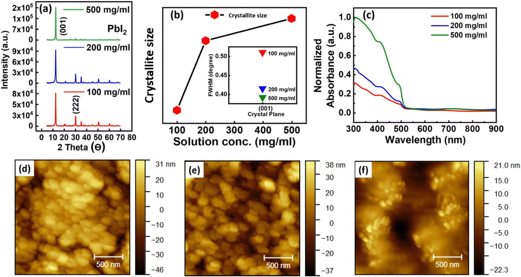 | ||
| Fig. 1 (a) Series of XRD pattern of 100, 200 and 500 mg ml−1 solution concentration. (b) Crystallite size extracted from XRD data, and inset represents the FWHM graph of dominant (001) crystal growth plane. (c) UV-Vis spectra of all three PbI2 thin films. (d),–(f) AFM images of thin films prepared with 100, 200, and 500 mg ml−1 solution concentration, respectively. | ||
As the concentration of PbI2 increases, the (β) value of full-width half-maximum (FWHM) gradually decreases and crystallite size (D) increases respectively, as shown in the inset of Fig. 1b.30 The average crystallite size of PbI2 crystals of three different solution concentrations thin films was obtained using the Debye Scherrer equation.
| (αhv)n = A(hv − Eg) |
Electrical performance
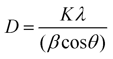
Fig. 2a shows the memristor device configuration used in this work, PET/ITO/PEDOT:PSS/PbI2/Ag (complete details of the fabrication procedure are discussed in the experimental section). ITO (indium tin oxide) is the bottom electrode (BE) as a non-hysteretic inert electrode, and silver (Ag) is used as the top electrode (TE) with a ∼1.0 mm2 device area. The current–voltage (I–V) characteristics of the devices were measured by applying DC cyclic voltage sweep of 1 volt. I–V characteristics were probed by applying external bias to the TE and BE was grounded throughout the electrical measurements. All measurements were performed in ambient environment conditions.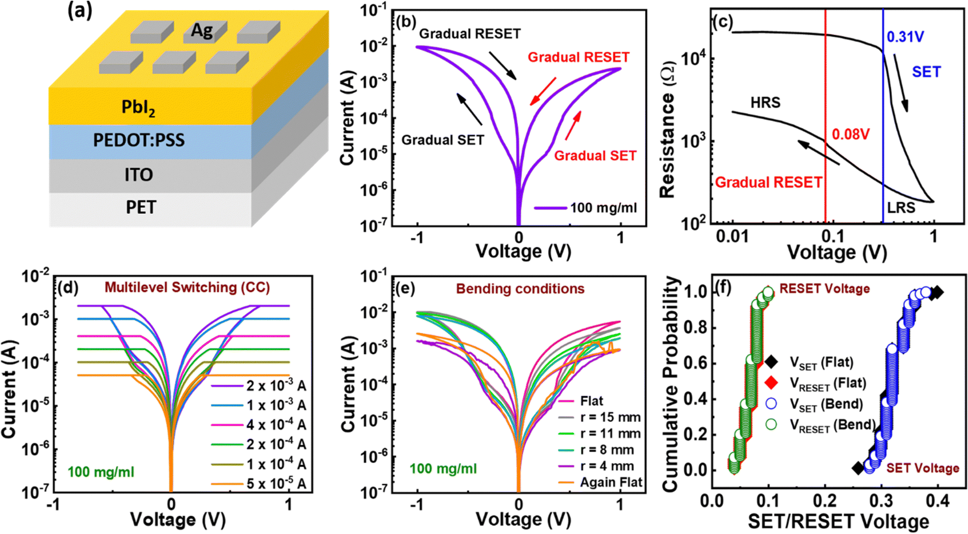 | ||
| Fig. 2 (a) Schematic diagram of device configuration. I–V characteristics of the device with solution concentration 100 mg ml−1, (b) demonstrating gradual SET and RESET process on both the polarities, (c) replotted with respect to resistance on log scale (i.e., log (V)–log (R)), (d) with varying current compliance, (e) I–V on flat and different bending radii (r = 15, 11, 8, and 4 mm) and then again on flat condition. (f) Cumulative probability of SET/RESET voltage of 100 consecutive I–V cycles of 100 mg ml−1 device on flat and maximum bending condition (4 mm). | ||
Fig. 2b illustrates the analog hysteresis observed in the as-prepared device when subjected to a DC voltage sweep (0 V → 1 → 0 → −1 → 0 V), at the voltage scan speed of 400 mV s−1.32 The device shows analog and unipolar switching characteristics with a low threshold (SET) voltage of 0.3 V and RESET voltage of 0.08 V shown in Fig. S6 (ESI†). The power consumption of the device is estimated to be 10 micro joules (μJ) which is attributed to its low SET/RESET voltage as 0.3/0.08 V, respectively.
In particular, analog memristor exhibits artificial synapses characteristics for neuromorphic computing which are inspired by the human brain.33 The device with the smallest grain size and more grain boundaries (i.e., 100 mg ml−1) demonstrate consistent and higher hysteresis loop area compared to the other two devices (Fig. S5, ESI†). No significant current level difference was observed for devices prepared with solution concentrations 100 and 200 mg ml−1 but the current value dropped by ∼1 order for 500 mg ml−1 solution concentration, attributed to the higher series resistance in later devices as a result of high thickness.34 Here, grain boundaries are the percolation pathways for the migration of vacancies/ions to control the resistance states (HRS and LRS) and their transition and thereby result in resistive switching.35–37 As the device is unipolar, the switching of resistance state from HRS to LRS and later switching back from LRS to HRS is termed as SET and RESET process respectively, both process occurs at the same voltage polarity. Unlike, various other memristor devices usually require positive voltage to SET the device and negative voltage to RESET the device or vice-versa, unipolar device does not require two different voltage polarity to undergo SET and RESET processes.38–40 Based on the I–V characteristics, devices prepared using 100 mg ml−1 PbI2 solution is used for the further investigation.
Due to unipolar behaviour of the device, identical nature of I–V characteristics can be observed on the opposite side (i.e., negative) polarity voltage. The analog behavior of the device is due to the absence of hopping mechanism. To confirm the gradual SET and RESET process and to validate the analog switching of device, the resistance obtained from I–V characteristics of the device at positive (Fig. 2c) and negative (Fig. S7, ESI†) polarity voltage are plotted on logarithmic scale. Under the positive voltage scan, weak and thin conducting filaments are formed via metal ions as well as ions and vacancies from the PbI2 layer. The formation and rupture of these filaments are referred to as the SET and RESET processes. It is important to recognize that the RESET process fails to fully restore the initial resistance values owing to some remnant weak filaments. The non-linear I–V characteristics observed in Fig. 2b and c is a result of the incomplete RESET process. Furthermore, the optimum voltage, scan speed, and current compliance (CC) for these devices are shown in Fig. S8–S10 (ESI†). Multilevel switching characteristics (Fig. 2d) was confirmed by varying CC as 10−3 A, 10−4 A, and 10−5 A. The HRS state remains the same but the LRS state increases with the decrease in CC which indicates the LRS state can be controlled by varying the CC during the SET process41 (Fig. 2d). Further, the continuous drop of the LRS from data retention characteristics confirms the volatile nature of PbI2 based memristor devices. (Fig. S11, ESI†)
To explore the potential of this device for flexible applications, I–V characteristics were measured at different bending radii of 15 mm, 11 mm, 8 mm, 4 mm and back to flat condition as shown in Fig. 2e. The flexible memristor device based on PbI2 demonstrates remarkable mechanical stability, a crucial trait for its effective utilization in flexible applications. The switching behavior in I–V remains invariant up to 8 mm bending radius. Further bending of the substrate at 4 mm radius leads to a significant drop in one-order current level and hysteresis. However, the consequent I–V scan on flat condition (after bending condition) shows the attempt to reinstate of switching pattern. The stability of a structure under external stress is important for a flexible memristor. The excellent stability of the device structure can be assigned to the stability of PbI2. From the literature, it can be confirmed that PbI2 has an elastic constant (14.69 N m−1) enabling mechanically stable under distortion, smaller possion's ratio leads to material stability under sheer force and sheer modulus (γ0/G2D) > 1.75 which states the material is ductile.42 To investigate the reproducibility of device under mechanical stress, 100 consecutive I–V characteristics were measured at 4 mm bending conditions (Fig. S12a, ESI†). Also, to check the mechanical stability of device under flat and bending conditions, the operational switching parameters of the device (i.e., SET and RESET voltage) were plotted using cumulative probability with invariant performance (Fig. 2f). The remarkable mechanical stability of PbI2 can be attributed to the combination of ionic bonding, where oppositely charged ions attract and hold the structure together, along with weak van der Waals forces that operate between I–Pb–I layered arrangements. These interatomic forces contribute to the cohesive and stable nature of the material.42
 | ||
| Fig. 3 Switching mechanism: (a) I–V characteristics by varying top electrode initiating with highly active Silver (Ag) electrode, less active copper (Cu) electrode, partially inert graphite electrode and highly inert electrode gold (Au). Log (V)–log (R) graph of I–V characteristics. (b) Log (I)–log (V) graph with conduction mechanisms. For gradual SET process via: (c) charge injection region (0–0.32 V). (d) Trap Assisted Tunneling region (TAT) (0.32–0.37 V). (e) Space charge limited current (SCLC) region (0.38–1 V). For gradual RESET process: (f) Schottky emission region (1–0.08 V). | ||
The proposed conduction mechanism behind the switching behavior of PbI2 memristor device is investigated by replotting the I–V curve using log scale i.e., log (V) vs. log (I) of positive polarity region shown in Fig. 3b. The conduction mechanism is divided and fitted into various regions: Charge injection region, trap-assisted tunnelling region (TAT), Space charge limited current region (SCLC), and Schottky emission (SE). Initially, the charge injection region as Ohmic region (I α V) is observed in 0–0.32 V voltage region with 1.1 slope value (Fig. 3c and Fig. S14b, ESI†), referring to the injection/migration of charge metal ions/carriers from TE into the active layer to initiate the filament formation process.45–47 On further increase of voltage (0.32–0.38 V), TAT mechanism (ln (I) α 1/V) is observed (Fig. 3d), entails two-stage process, where carriers are first captured by defects or vacancies and subsequently tunnel through a barrier to reach another trap.48–50 The gradual rise in current signifies the formation of vacancies that establish the conduction path. Furthermore, as the traps within the material are occupied, the space-charge-limited current (SCLC, I α V2) mechanism (Fig. 3e) dominates in the voltage range (0.38–1.0 V). As the voltage is applied in reverse direction (1–0.08 V) the the Schottky Emission (SE) mechanism (ln (I) and V1/2) comes into play. The SE mechanism aids in facilitating the escape of trapped charges, further resetting the device (Fig. 3g). Finally, as the voltage decreases to a low bias range of 0.08 V to 0 V, the device returns to HRS, forming Ohmic conduction characterized by a linear relationship between current and voltage (I α V), as depicted in Fig. S15 (ESI†). Since the device is unipolar, the RESET process also occurs gradually in the same polarity.
Synaptic measurements
Memristors are commonly investigated with respect to their emulation of certain functions of biological neurons, particularly in the context of artificial synapses.51Fig. 4a shows the schematic diagram indicating the structural relationship between neural synapse and artificial synapse. An artificial synapse can be conceptualized as a two-terminal device capable of dynamically adjusting and retaining its synaptic weights through the utilization of voltage spikes.52Fig. 4(a) clearly illustrates the TE (Ag) and BE (ITO) electrodes as the input and output for pre-synaptic and post-synaptic voltage spikes respectively, while the conductance of the active layer represents the synaptic cleft. In a biological synapse, when a stimulus reaches the pre-synaptic neuron, the influx of calcium ions (Ca2+) prompts the release of neurotransmitters into the synaptic cleft, which then affects the post-synaptic neuron.53 Similarly in an artificial synapse, under the influence of an electric field, these ions inoculates into the active layer and changes the conductance of device.54 Due to the strong mechanical and electrical stability, the devices fabricated with the solution concentration 100 mg ml−1 were later used for synaptic characterizations.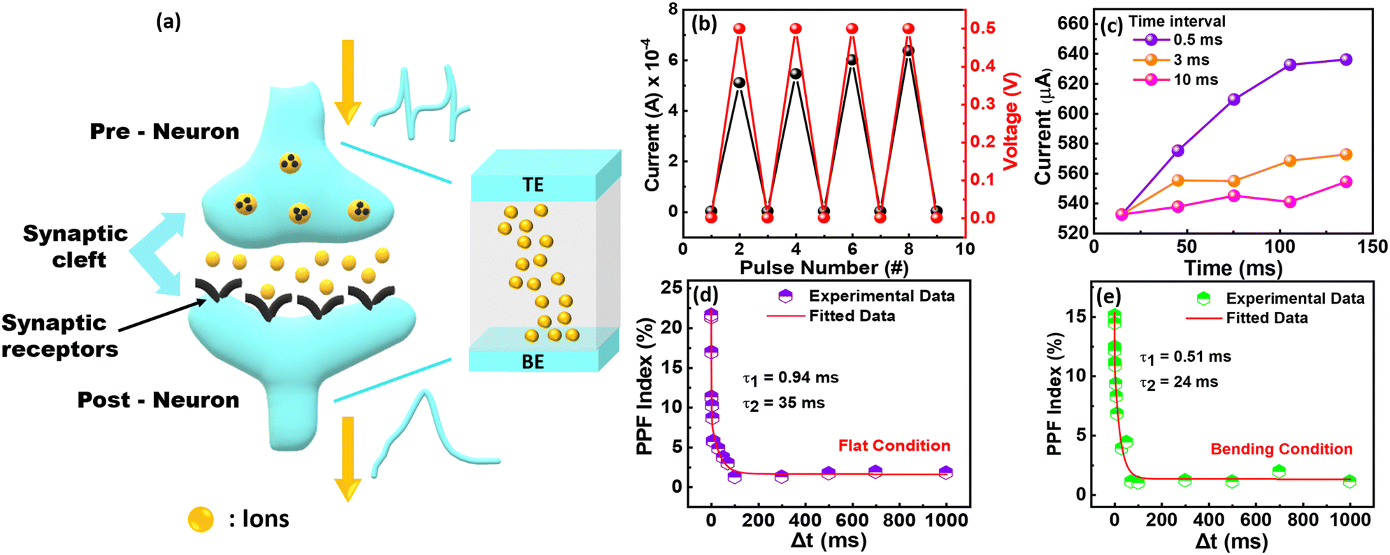 | ||
| Fig. 4 (a) Illustration of the biological and artificial synapse (b) current response induced by a pair of pre-synaptic pulses, (c) variation in current during pre-synaptic pulses for different time intervals. PPF index for (e) flat condition and (f) bending condition (r = 4 mm). | ||
The paired-pulse facilitation (PPF) characteristic, a type of short-term synaptic plasticity, describes the dynamic intensification of neurotransmitters in biological brain synapses, involved in a variety of neural functions like simple learning and memorizing information.55 PPF can be simplified as the degree of facilitation between the first and second pre-synaptic voltage spikes.56 When the identical pulses of bias 0.5 V were applied to TE as input voltage spike the corresponding current response is noted as output which increases with every consecutive applied pulse of voltage with time interval 0.1 ms (Fig. 4b). With increasing duration of time interval,55 PPF was recorded following a similar procedure as described previously where the current magnitude decreases with the increase of the time interval between two consecutive pulses. Fig. 4c illustrates the current response recorded when applying identical pairs of pre-synaptic voltage pulses at varying time intervals. As the time interval between two consecutive pulses of voltage is too short, mobile ions gathered at the interface will not have enough time to diffuse back before the arrival of second pulse of voltage. Hence, the second spike has more potential than the first spike. This increase in current was calculated by PPF index using equation 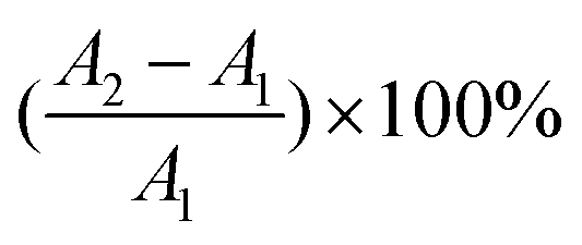 (A1 and A2 are the current amplitude at successive volatge pulses) for both flat and bending condition (r = 4 mm). The decay of PPF index with time interval was fitted using double exponential decay function.57
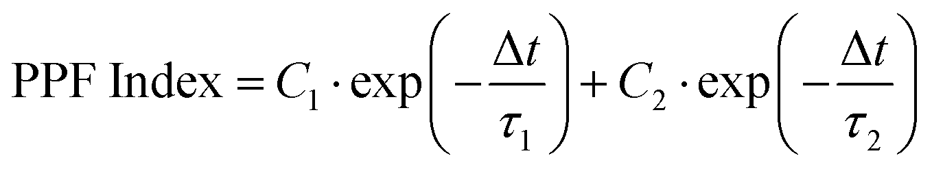 where, C1 and C2 represent the initial magnitudes and τ1 and τ2 are the characteristic relaxation time of the rapid and slow decay respectively.58 The extracted relaxation time constant values are τ1 = 0.94 ms and τ2 = 35 ms for flat condition while τ1 = 0.51 ms and τ2 = 24 ms for bending condition corresponding to fast and slow decay terms as observed in Fig. 4d and 4e respectively. The extracted values closely resemble the time constants observed in biological synapses, where τ1 is typically in the range of tens of milliseconds (rapid phase) and τ2 is in the range of hundreds of milliseconds (slow phase).59–61 PPF index increases for short time intervals while decreases for long time intervals imitating biological synaptic response.
The learning and forgetting behavior of artificial synapse can also be represented by potentiation and depression (P&D).62 This behavior can be attributed to the formation and rupture of filament formed due to metal or halide ions. Generally, P&D pattern depends on the pulse amplitude and time interval. The first pattern of P&D was obtained with identical pulses of 1.0 V and 0.35 V respectively (Fig. 5a) with read voltage of 0.25 V. Due to device's unipolar nature, it potentiates and depresses in the same polarity. Fig. 5b shows the multiple cycles of P&D taken using an identical pulse method. As observed the P&D is non-linear which is not a good characteristic for an artificial synaptic device for its application in neural networks, which should be linear ideally. Ensuring a gradual and incremental increase in conductance while maintaining linearity is fundamental for the proper functioning of artificial neural networks (ANNs).63 To reduce the non-linearity nature, non-identical pulses method in step increasing mode from 0.05–1 V was recorded (Fig. 5c) which enable it to implement for neural networking applications.64 The operational stability was confirmed by measuring P&D up to 2 × 10⁴ cycles as shown in Fig. 5d with 1st and 20Kth cycle on flat condition (Fig. S16, ESI†). To validate the flexibility of device same data was collected on bending condition (r = 4 mm) as shown in Fig. 5e. The higher level of current on bending condition compared to flat condition is attributed to the easier formation and rupture of the filament. As the device is bended, it is hypothesized the distance between the active layer and TE reduces providing a quick path for conduction and increasing the current level of the device. The non-linearity (NL) factor of P&D with identical pulses (35% and 33%) and non-identical pulses (1.58% and 1.49%) in flat and bending condition (Fig. 5f) is calculated using equation 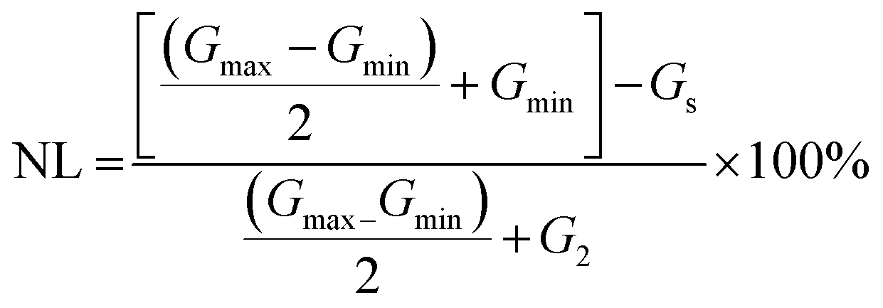 . Here, the Gmax, Gmin are maximum conductance, minimum conductance used to switch the device between maximum and minimum conductance states, respectively.65 It is noteworthy that, both linearity and symmetry of P&D are important factors for neuromorphic computing. The symmetry of the device is estimated from the above calculated non-linearity values of P&D. The non-linearity of device with identical pulses is αp = 0.35 for potentiation and αd = 0.33 for depression, while the same device with non-identical pulses shows αp = 0.0158 for potentiation and αd = 0.0149 for depression. Hence, the asymmetry value for identical pulses is 0.2 while with non-identical pulses is 0.0009. These values are directly extracted from experimental results.66
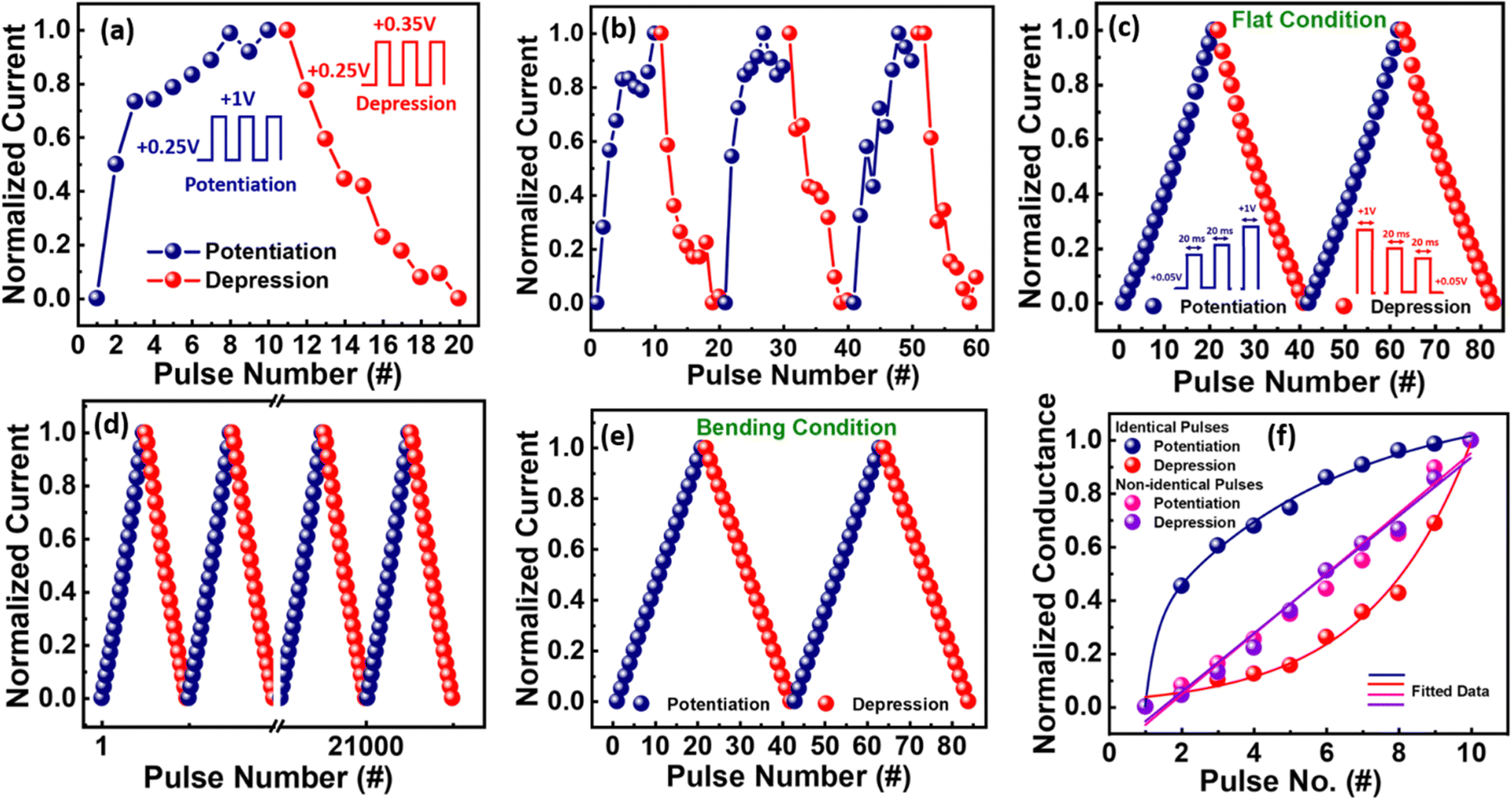 | ||
| Fig. 5 (a) Single P&D cycle by giving identical pulses of 1 V with constant read voltage of 0.25 V. (b) Multiple cycles of P&D via identical pulses pattern. (c) and (d) are P&D obtained by non-identical pulse method in flat condition. (e) P&D cycles in bending condition obtained by non-identical pulse method. (f) Non-linearity factor calculated for P&D obtained by identical pulse and non-identical pulse method. | ||
In a biological synapse, synaptic plasticity is a phenomenon that encompasses variations in synaptic strength and synaptic connectivity and is believed to serve as the primary mechanism for memory formation and learning processes in a human brain.67 In an artificial synapse, synaptic plasticity refers to the change in conductance (synaptic weight) which results in primary synaptic characteristics such as P&D and PPF etc. An advanced form of learning by Hebbian learning is termed as STDP, where the chronological order and time interval between the pre-and postsynaptic spikes affect the change and direction of the synaptic weight.68,69 STDP functions by modifying the synaptic weight based on the relative timing of spikes between the pre-synaptic and post-synaptic neurons. This timing is represented by Δt (Δt = tpre − tpost), where tpre indicates the arrival time of the pre-synaptic neuron spike, and tpost represents the arrival time of the post-synaptic neuron spike.70 When presynaptic stimulation precedes postsynaptic activity (Δt > 0), it leads to an enhancement in synaptic efficiency, ultimately resulting in long-term potentiation (LTP). Conversely, when postsynaptic stimulation precedes presynaptic activity (Δt < 0), it diminishes efficiency, leading to long-term depression (LTD).69 The elapsed period between the pre- and post-synaptic pulses controls the magnitude of the subsequent alterations in synaptic weight. Synaptic plasticity in memristors is achieved by gradually switching between the HRS and LRS in response to trains of pulses with changing pulse widths. Four STDP patterns (asymmetric Hebbian STDP, asymmetric anti-Hebbian STDP, symmetric Hebbian STDP, and symmetric anti- Hebbian STDP) were collected simultaneously on both flat as well as bending condition of radius r = 4 mm (Fig. 6a–d). Regarding these, the weight updates can be represented by the following equations: Δws = A![[thin space (1/6-em)]](https://www.rsc.org/images/entities/char_2009.gif) exp(−Δt/τ) + Δw0 denotes asymmetric STDP while Δwa = Aexp(−Δt2/τ2) + Δw0 denotes symmetric STDP, Δw0 is the constant signifying a non-associative component of the synaptic change, A is the scaling factor and τ is the time constant. The experimental data was analyzed by fitting it with two different mathematical functions: the exponential function, and the Gaussian function. The pre and post synaptic pulse mode adopted to get the STDP patterns are shown in Fig. S17 (ESI†). The fastest biological synaptic transmission typically occurs within a time frame ∼1 ms. This refers to the speed at which signals are transmitted across synapses in the nervous system. Herein, PbI2 based flexible memristor device demonstrates similar communication time (∼3 ms) of human brain and shows the potential for the neuromorphic computing application.71,72
exp(−Δt/τ) + Δw0 denotes asymmetric STDP while Δwa = Aexp(−Δt2/τ2) + Δw0 denotes symmetric STDP, Δw0 is the constant signifying a non-associative component of the synaptic change, A is the scaling factor and τ is the time constant. The experimental data was analyzed by fitting it with two different mathematical functions: the exponential function, and the Gaussian function. The pre and post synaptic pulse mode adopted to get the STDP patterns are shown in Fig. S17 (ESI†). The fastest biological synaptic transmission typically occurs within a time frame ∼1 ms. This refers to the speed at which signals are transmitted across synapses in the nervous system. Herein, PbI2 based flexible memristor device demonstrates similar communication time (∼3 ms) of human brain and shows the potential for the neuromorphic computing application.71,72
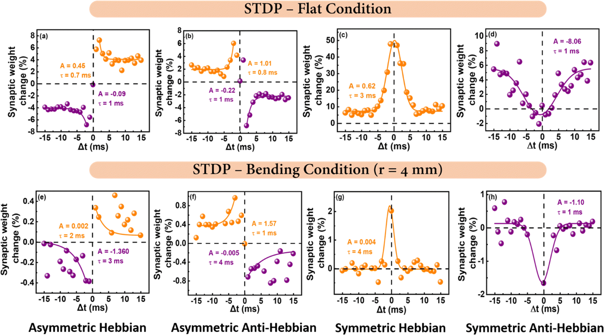 | ||
| Fig. 6 Spike time-dependent plasticity (STDP) characterization of PbI2 based memristor device in flat and bending condition respectively (a) and (e) Asymmetric Hebbian, (b) and (f) Asymmetric anti-Hebbian, (c) and (g) Symmetric Hebbian (d) and (h) Symmetric anti-Hebbian. | ||
To scale the efficacy of PbI2-based memristors as an artificial synapse, a multilayer perceptron simulation was conducted within a four-layer neural network as illustrated in Fig. 7a.73 More details of the simulation can be found in the literature.74,75 Here four-layer neural network comprises an input layer with 784 neurons, two hidden layers with 250 and 125 neurons respectively, and an output layer with 10 neurons.76 The input layer here offers the MNIST handwritten images data set ranging from (0 to 9) with dimensions 28 × 28 pixels and the hidden layer uses the simplified input feature based on the synaptic weight matrix. Every layer of neurons was intricately linked by synapses, and the synaptic weight was updated through fee-forward and back-propagation processes.77 During each epoch, 50 000 MNIST training data set images and 10 000 MNIST test set images were employed for training and testing respectively. For mapping of the weights, the measured lowest and highest conductance states are ‘0’ and ‘1’, respectively. The states between ‘0’ and ‘1’ have intermediate weights and the nonlinearity is considered during weights mapping. The difference between adjacent conductance states is used to determine the linearity of the mapped synaptic plasticity. Furthermore, different conductance states were achieved by applying pulses. Synaptic weights in the training process were selected from P&D curves (200 conductance states) based on parameters such as less non-linearity(∼1%), dynamic range, and precision extracted from (Fig. 5c and f). After 30 epochs of training, the PbI2 device exhibited a commendable recognition accuracy of 95.04% for flat condition and 95.06% for bending condition of 4 mm, as shown in Fig. 7b. Table S1 (ESI†) contains a comparison chart in the literature depicting accuracy in relation to the number of training epochs. A parallel simulation was executed utilizing an ideal synaptic device characterized by perfect linearity (AP = AD = 0), endless dynamic range, and an unlimited range of conductance states. This idealized set-up achieved a higher accuracy of 97.07%. In contrast, the performance of PbI2 is very close and promising, placing it as a forthcoming nominee for artificial synapses in neuromorphic computing for flexible applications.
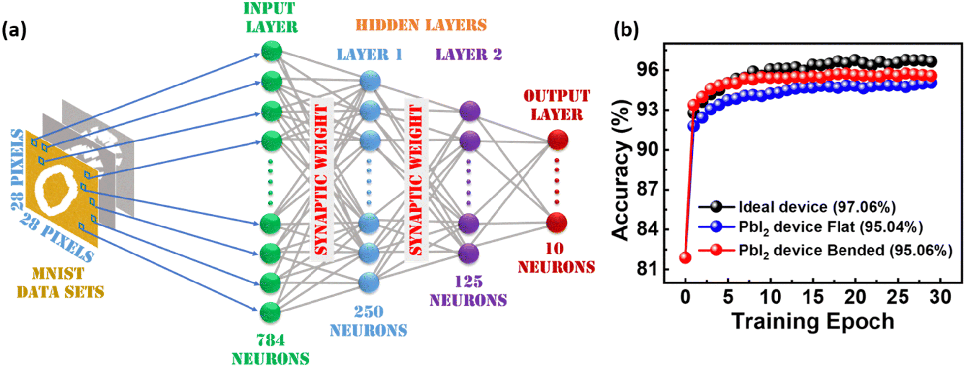 | ||
| Fig. 7 (a) Schematic of the four-layer neural network for the pattern recognition simulation. Each node symbolizes the neuron, and each connection symbolizes the synapse. (b) Pattern recognition accuracies based on the ideal and the PbI2 synaptic device on flat and bending condition (r = 4 mm). | ||
Conclusions
In this work, we developed a remarkably stable and flexible low-voltage operating memristor device by a complete solution process, focusing the applications in data storage and neuromorphic computation. These findings explore the impact of solution concentration on thin film thickness, morphology, and the underlying mechanism behind resistive switching and also, aim to develop novel flexible artificial neural synapses that can replicate the crucial functions exhibited by biological synapses in the brain. Moreover, this research delves into the significance of ion migration and the formation/rupture of conductive filaments in resistive switching-based artificial neural synapses. It also uncovers the benefits associated with these phenomena. Additionally, an environmentally robust device has been fabricated and assessed under ambient air conditions (with 75% relative humidity), without the need for any encapsulation. These devices demonstrate unipolar analog resistive switching with strong mechanical stability when bended up to 4 mm radius. Major synaptic characterizations on both flat as well as bending condition are reported such as PPF, PPF index, P&D, and STDP. Also, MNIST pattern recognition accuracy was simulated as 95.04% and 95.06% on flat as well as bending conditions, respectively. In conclusion, our investigation demonstrates the reliable resistive switching behavior, coupled with commendable synaptic properties, in mechanically and environmentally stable lead iodide-based flexible memristive devices. These findings highlight the substantial potential of these device for applications in neuromorphic computation and information processing.Experimental methods
Materials
Lead(II) Iodide (PbI2, 99.999%, metal basis), PEDOT:PSS (1.3 wt% dispersion in H2O, conductive grade), DMF (anhydrous, 99.8%) were purchased from Sigma Aldrich and used as received. Precursor solutions of different concentrations (0.2 M, 0.4 M, and 1 M) were prepared by dissolving PbI2 in DMF. The solutions were continuously heated and stirred at 100 °C until clear solution was obtained.
Device fabrication procedure
Commercially available indium tin oxide (ITO) coated Polyethylene Teraphalate (PET) flexible substrate sheets were cleaned following standard cleaning procedure i.e., Substrates were ultrasonicated for 15 minutes each with soap solution followed by deionized water (DI water) and then mixture of acetone and isopropanol (IPA). By using UV-Ozonization the hydrophobic property of surface was changed to hydrophilic. The devices were fabricated layer by layer spin coating procedure. Initially, PEDOT: PSS was deposited on cleaned substrates by spin coating process at 4000 rpm for 1 minute followed by annealing for 15 minutes at 100 °C. Similarly, PbI2 layer was deposited at 3000 rpm for 1 minute followed by annealing for 20 minutes at 60 °C. Top electrode (Ag) of diameter ∼1 mm was deposited.Thin film and device characterizations
AFM was conducted for investigate the morphology of the PbI2 films. Surface topography and film thickness by cross section SEM by the ZEISS Ultra 55. UV-Visible spectroscopy was conducted to investigate the optical properties from SHIMADZU UV-1900i. Current–voltage sweep, and voltage pulse measurements were performed using the source measurement unit (SMU) Keithley 2604B in ambient conditions. An electrical module ArcONE was employed for STDP measurements.Conflicts of interest
There are no conflicts to declare.Acknowledgements
A. S. and M. J. gratefully acknowledge GUJCOST research grant GUJCOST/STI/2021-22/3873 from the government of Gujarat, India to support fabrication and electrical characterizations. A. S. and M. S. also acknowledge SHODH Grant (#2021015826) from the Gujarat government for investigation. A. G. thanks the MCIN for financial assistance under the project TAROT (PID2022-141850OB-C21). Authors would also like to thanks Mr. Parth Thakkar for his support and acknowledge Solar Research and Development Centre (SRDC), PDEU for supporting structural characterizations.References
- Y. H. Jung, T. X. Pham, D. Issa, H. S. Wang, J. H. Lee, M. Chung, B. Y. Lee, G. Kim, C. D. Yoo and K. J. Lee, Nano Energy, 2022, 101, 107610 CrossRef CAS.
- C. D. Schuman, S. R. Kulkarni, M. Parsa, J. P. Mitchell, P. Date and B. Kay, Nat. Comput. Sci., 2022, 2, 10–19 CrossRef.
- F. Staudigl, F. Merchant and R. Leupers, IEEE Des. Test, 2022, 39, 90–99 Search PubMed.
- M. Kumar, J. Lim and H. Seo, Nano Energy, 2021, 89, 106471 CrossRef CAS.
- Q. Liu, L. Yin, C. Zhao, Z. Wu, J. Wang, X. Yu, Z. Wang, W. Wei, Y. Liu, I. Z. Mitrovic, L. Yang, E. G. Lim and C. Z. Zhao, Nano Energy, 2022, 97, 107171 CrossRef CAS.
- G. Zhou, Z. Ren, L. Wang, J. Wu, B. Sun, A. Zhou, G. Zhang, S. Zheng, S. Duan and Q. Song, Nano Energy, 2019, 63 Search PubMed.
- P. Xu, D. Lan, F. Wang and I. Shin, Electron, 2023, 12, 1–15 Search PubMed.
- R. Li, W. Wang, Y. Li, S. Gao, W. Yue and G. Shen, Nano Energy, 2023, 111, 108398 CrossRef CAS.
- X. Yan, X. Jia, Y. Zhang, S. Shi, L. Wang, Y. Shao, Y. Sun, S. Sun, Z. Zhao, J. Zhao, J. Sun, Z. Guo, Z. Guan, Z. Zhang, X. Han and J. Chen, Nano Energy, 2023, 107, 108091 CrossRef CAS.
- A. Sengupta and K. Roy, Phys. Rev. Appl, 2016, 5 Search PubMed.
- T. Ohno, T. Hasegawa, T. Tsuruoka, K. Terabe, J. K. Gimzewski and M. Aono, Nat. Mater., 2011, 10, 591–595 CrossRef CAS PubMed.
- R. D. Raninga, R. A. Jagt, S. Béchu, T. N. Huq, W. Li, M. Nikolka, Y. H. Lin, M. Sun, Z. Li, W. Li, M. Bouttemy, M. Frégnaux, H. J. Snaith, P. Schulz, J. L. MacManus-Driscoll and R. L. Z. Hoye, Nano Energy, 2020, 75, 104946 CrossRef CAS.
- A. Solanki, M. M. Tavakoli, Q. Xu, S. S. H. Dintakurti, S. S. Lim, A. Bagui, J. V. Hanna, J. Kong and T. C. Sum, Adv. Mater., 2020, 32, 1–11 CrossRef PubMed.
- S. V. N. Pammi, R. Maddaka, V. D. Tran, J. H. Eom, V. Pecunia, S. Majumder, M. D. Kim and S. G. Yoon, Nano Energy, 2020, 74, 104872 CrossRef CAS.
- L. Sun, C. Wang, L. Xu, J. Wang, X. Chen and G. C. Yi, J. Mater. Chem. C, 2018, 6, 7188–7194 RSC.
- D. D. Vo, M. Idrees, V. T. Pham, T. V. Vu, S. T. Nguyen, H. V. Phuc, N. N. Hieu, N. T. T. Binh, B. Amin and C. V. Nguyen, Chem. Phys., 2020, 533, 110736 CrossRef CAS.
- N. Preda, L. Mihut, M. Baibarac, I. Baltog and S. Lefrant, J. Phys.: Condens. Matter., 2006, 18, 8899–8912 CrossRef CAS.
- W. T. Wang, J. Sharma, J. W. Chen, C. H. Kao, S. Y. Chen, C. H. Chen, Y. C. Feng and Y. Tai, Nano Energy, 2018, 49, 109–116 CrossRef CAS.
- H. Zhong, X. Liu, M. Liu, S. Yin, Z. Jia, G. Fu, S. Yang and W. Kong, Nano Energy, 2023, 105, 108014 CrossRef CAS.
- A. Solanki, P. Yadav, S. H. Turren-Cruz, S. S. Lim, M. Saliba and T. C. Sum, Nano Energy, 2019, 58, 604–611 CrossRef CAS.
- M. Manjappa, A. Solanki, A. Kumar, T. C. Sum and R. Singh, Adv. Mater., 2019, 31, 1901455 CrossRef PubMed.
- E. Wlaźlak, M. Marzec, P. Zawal and K. Szaciłowski, ACS Appl. Mater. Interfaces, 2019, 11, 17009–17018 CrossRef PubMed.
- D. Acuña, B. Krishnan, S. Shaji, S. Sepúlveda and J. L. Menchaca, Bull. Mater. Sci., 2016, 39, 1453–1460 CrossRef.
- N. M. Adenam, M. Y. A. M. Yunin, W. M. Khairul, A. H. Yusoff and H. K. Adli, Chem. Phys. Impact, 2022, 5, 100116 CrossRef.
- J. F. Condeles, R. C. Z. Lofrano, J. M. Rosolen and M. Mulato, Braz. J. Phys., 2006, 36, 320–323 CrossRef CAS.
- S. Ngqoloda, C. J. Arendse, T. F. Muller, S. S. Magubane and C. J. Oliphant, Coatings, 2020, 10, 1–13 CrossRef.
- D. B. Khadka, Y. Shirai, M. Yanagida, T. Masuda and K. Miyano, Sustainable Energy Fuels, 2017, 1, 755–766 RSC.
- J. M. C. Da Silva Filho and F. C. Marques, MRS Adv., 2018, 3, 1843–1848 CrossRef.
- P. Basumatary and P. Agarwal, J. Mater. Sci.: Mater. Electron., 2020, 31, 10047–10054 CrossRef CAS.
- S. Aldawood, O. M. AlTalib, M. S. AlGarawi, T. S. Alkhuraiji, Y. Alashban, N. Shubayr, A. T. Abdul Rahman, K. Saeed and S. M. Ali, Radiat. Phys. Chem., 2022, 193, 110003 CrossRef CAS.
- W. Ma, F. Yang, Y. Wang, J. Chen, L. Yuan, D. Xie, Y. Zhao, Y. Zhang and J. Peng, J. Mater. Sci., 2017, 52, 9696–9708 CrossRef CAS.
- C. Gonzales and A. Guerrero, J. Phys. Chem. Lett., 2023, 14, 1395–1402 CrossRef CAS PubMed.
- Y. Li, J. Chu, W. Duan, G. Cai, X. Fan, X. Wang, G. Wang and Y. Pei, ACS Appl. Mater. Interfaces, 2018, 10, 24598–24606 CrossRef CAS PubMed.
- F. A. Jhuma, M. Z. Shaily and M. J. Rashid, Mater. Renewable Sustainable Energy, 2019, 8, 1–7 CrossRef.
- K. Sakhatskyi, R. A. John, A. Guerrero, S. Tsarev, S. Sabisch, T. Das, G. J. Matt, S. Yakunin, I. Cherniukh, M. Kotyrba, Y. Berezovska, M. I. Bodnarchuk, S. Chakraborty, J. Bisquert and M. V. Kovalenko, ACS Energy Lett., 2022, 7, 3401–3414 CrossRef CAS PubMed.
- X. Guan, Z. Lei, X. Yu, C. H. Lin, J. K. Huang, C. Y. Huang, L. Hu, F. Li, A. Vinu, J. Yi and T. Wu, Small, 2022, 18 Search PubMed.
- Y. Park and J. S. Lee, ACS Appl. Mater. Interfaces, 2022, 14, 4371–4377 CrossRef CAS PubMed.
- Y. V. Sakharov, IOP Conf. Ser. Mater. Sci. Eng., 2019, 498, 0–4 CAS.
- R. Midya, Z. Wang, M. Rao, N. K. Upadhyay and J. J. Yang, RRAM/memristor for computing, Elsevier Ltd., 2nd edn, 2019 Search PubMed.
- J. Domaradzki, D. Wojcieszak, T. Kotwica and E. Mańkowska, Int. J. Electron. Telecommun., 2020, 66, 373–381 Search PubMed.
- J. M. Yang, E. S. Choi, S. Y. Kim, J. H. Kim, J. H. Park and N. G. Park, Nanoscale, 2019, 11, 6453–6461 RSC.
- R. Ran, C. Cheng, Z. Y. Zeng, X. R. Chen and Q. F. Chen, Philos. Mag., 2019, 99, 1277–1296 CrossRef CAS.
- A. Solanki, A. Guerrero, Q. Zhang, J. Bisquert and T. C. Sum, J. Phys. Chem. Lett., 2020, 11463–11470 Search PubMed.
- M. Khemnani, B. Tripathi, P. Thakkar, J. Gosai, M. Jain, P. Chandra and A. Solanki, ACS Appl. Electron. Mater., 2023, 5, 5249–5256 CrossRef CAS.
- Y. T. Su, K. C. Chang, T. C. Chang, T. M. Tsai, R. Zhang, J. C. Lou, J. H. Chen, T. F. Young, K. H. Chen, B. H. Tseng, C. C. Shih, Y. L. Yang, M. C. Chen, T. J. Chu, C. H. Pan, Y. E. Syu and S. M. Sze, Appl. Phys. Lett., 2013, 103 Search PubMed.
- K. Jung, Y. Kim, H. Im, H. Kim and B. Park, J. Korean Phys. Soc., 2011, 59, 2778–2781 CrossRef CAS.
- F. Y. Yuan, N. Deng, C. C. Shih, Y. T. Tseng, T. C. Chang, K. C. Chang, M. H. Wang, W. C. Chen, H. X. Zheng, H. Wu, H. Qian and S. M. Sze, Nanoscale Res. Lett., 2017, 12, 3–8 CrossRef PubMed.
- P. Mainali, P. Wagle, C. McPherson and D. N. McIlroy, Science, 2023, 5 Search PubMed.
- F. M. Puglisi, P. Pavan, A. Padovani and L. Larcher, Solid-State Electron., 2014, 102, 69–75 CrossRef CAS.
- N. Raghavan, K. L. Pey and K. Shubhakar, Microelectron. Reliab., 2014, 54, 847–860 CrossRef CAS.
- A. Serb, A. Corna, R. George, A. Khiat, F. Rocchi, M. Reato, M. Maschietto, C. Mayr, G. Indiveri, S. Vassanelli and T. Prodromakis, Sci. Rep., 2020, 10, 1–7 CrossRef PubMed.
- O. Kapur, D. Guo, J. Reynolds, Y. Han, R. Beanland, L. Jiang, C. H. de Groot and R. Huang, Adv. Electron. Mater., 2022, 8 Search PubMed.
- M. Shi, M. Zhang, S. Yao, Q. Qin, M. Wang, Y. Wang, N. He, J. Zhu, X. Liu, E. Hu, J. Xu and Y. Tong, J. Phys. Conf. Ser., 2020, 1631 Search PubMed.
- X. Zhang, S. Liu, X. Zhao, F. Wu, Q. Wu, W. Wang, R. Cao, Y. Fang, H. Lv, S. Long, Q. Liu and M. Liu, IEEE Electron Device Lett., 2017, 38, 1208–1211 CAS.
- L. A. Santschi and P. K. Stanton, Brain Res., 2003, 962, 78–91 CrossRef CAS PubMed.
- K. W. Park and W. J. Cho, Nanomaterials, 2022, 12 Search PubMed.
- S. H. Kim and W. J. Cho, Int. J. Mol. Sci., 2021, 22, 1–8 CAS.
- K. Wang, J. Chen and X. Yan, Nano Energy, 2021, 79, 105453 CrossRef CAS.
- R. S. Zucker and W. G. Regehr, Annu. Rev. Physiol., 2002, 64, 355–405 CrossRef CAS PubMed.
- A. Morrison, M. Diesmann and W. Gerstner, Biol. Cybern., 2008, 98, 459–478 CrossRef PubMed.
- Y. Wang, L. Yin, W. Huang, Y. Li, S. Huang, Y. Zhu, D. Yang and X. Pi, Adv. Intell. Syst., 2021, 3, 2000099 CrossRef.
- B. Y. Kim, H. G. Hwang, J. U. Woo, W. H. Lee, T. H. Lee, C. Y. Kang and S. Nahm, NPG Asia Mater., 2017, 9, e381–9 CrossRef CAS.
- H.-M. Huang, Z. Wang, T. Wang, Y. Xiao and X. Guo, Adv. Intell. Syst., 2020, 2, 2000149 CrossRef.
- A. Saleem, D. Kumar, F. Wu, L. B. Keong and T. Y. Tseng, IEEE Trans. Electron Devices, 2023, 70, 1351–1358 CAS.
- D. Ielmini, Microelectron. Eng., 2018, 190, 44–53 CrossRef CAS.
- Y. Zhu, Y. He, C. Chen, L. Zhu, H. Mao, Y. Zhu, X. Wang, Y. Yang, C. Wan and Q. Wan, Appl. Phys. Lett., 2022, 120 CAS.
- V. M. Ho, J. A. Lee and K. C. Martin, Science, 2011, 334, 623–628 CrossRef CAS PubMed.
- X. Yan, C. Qin, C. Lu, J. Zhao, R. Zhao, D. Ren, Z. Zhou, H. Wang, J. Wang, L. Zhang, X. Li, Y. Pei, G. Wang, Q. Zhao, K. Wang, Z. Xiao and H. Li, ACS Appl. Mater. Interfaces, 2019, 11, 48029–48038 CrossRef CAS PubMed.
- L. G. Wang, W. Zhang, Y. Chen, Y. Q. Cao, A. D. Li and D. Wu, Nanoscale Res. Lett., 2017, 12 Search PubMed.
- Y. Shuai, X. Pan and X. Sun, Spike-Timing-Dependent Plasticity in Memristors, Memristor and Memristive Neural Networks, 2018 DOI:10.5772/intechopen.69535.
- Y. Wu, H. Huang, C. Xu, X. Cao, Z. Lei, J. Zhang, Y. Zhao, A. Wei and Z. Liu, Appl. Phys. A: Mater. Sci. Process., 2023, 129, 1–8 CrossRef.
- Y. N. Zhong, T. Wang, X. Gao, J. L. Xu and S. D. Wang, Adv. Funct. Mater., 2018, 28, 1–6 Search PubMed.
- T. C. Südhof, J. Cell Biol., 2021, 220, 1–18 CrossRef PubMed.
- S. Choi, S. Jang, J. H. Moon, J. C. Kim, H. Y. Jeong, P. Jang, K. J. Lee and G. Wang, NPG Asia Mater., 2018, 10, 1097–1106 CrossRef CAS.
- C. H. Huang, H. Chang, T. Y. Yang, Y. C. Wang, Y. L. Chueh and K. Nomura, ACS Appl. Mater. Interfaces, 2021, 13, 52822–52832 CrossRef CAS PubMed.
- L. Liu, P. A. Dananjaya, M. Y. Chee, G. J. Lim, C. X. X. Lee and W. S. Lew, ACS Appl. Mater. Interfaces, 2023, 15, 29287–29296 CrossRef CAS PubMed.
- G. Noh, H. Song, H. Choi, M. Kim, J. H. Jeong, Y. Lee, M. Y. Choi, S. Oh, M. Kyung Jo, D. Y. Woo, Y. Jo, E. Park, E. Moon, T. S. Kim, H. J. Chai, W. Huh, C. H. Lee, C. J. Kim, H. Yang, S. Song, H. Y. Jeong, Y. S. Kim, G. H. Lee, J. Lim, C. G. Kim, T. M. Chung, J. Y. Kwak and K. Kang, Adv. Mater., 2022, 34, 1–11 CrossRef PubMed.
Footnote |
| † Electronic supplementary information (ESI) available. See DOI: https://doi.org/10.1039/d3nh00505d |
| This journal is © The Royal Society of Chemistry 2024 |