
 Open Access Article
 This Open Access Article is licensed under a
 Creative Commons Attribution 3.0 Unported Licence
Advancements in nanomaterials for nanosensors: a comprehensive review
Moustafa A.
Darwish
 *a,
Walaa
Abd-Elaziem
bc,
Ammar
Elsheikh
de and
Abdelhameed A.
Zayed
d
*a,
Walaa
Abd-Elaziem
bc,
Ammar
Elsheikh
de and
Abdelhameed A.
Zayed
d
aPhysics Department, Faculty of Science, Tanta University, Tanta 31527, Egypt. E-mail: mostafa_ph@yahoo.com; mostafa_ph@science.tanta.edu.eg
bDepartment of Mechanical Design and Production Engineering, Faculty of Engineering, Zagazig University, P.O. Box 44519, Egypt
cDepartment of Materials Science and Engineering, Northwestern University, Evanston, IL 60208, USA
dProduction Engineering and Mechanical Design Department, Faculty of Engineering, Tanta University, Tanta 31521, Egypt
eDepartment of Industrial and Mechanical Engineering, Lebanese American University, P.O. Box 36 / S-12, Byblos, Lebanon
First published on 24th May 2024
Abstract
Nanomaterials (NMs) exhibit unique properties that render them highly suitable for developing sensitive and selective nanosensors across various domains. This review aims to provide a comprehensive overview of nanomaterial-based nanosensors, highlighting their applications and the classification of frequently employed NMs to enhance sensitivity and selectivity. The review introduces various classifications of NMs commonly used in nanosensors, such as carbon-based NMs, metal-based NMs, and others, elucidating their exceptional properties, including high thermal and electrical conductivity, large surface area-to-volume ratio and good biocompatibility. A thorough examination of literature sources was conducted to gather information on NMs-based nanosensors' characteristics, properties, and fabrication methods and their application in diverse sectors such as healthcare, environmental monitoring, industrial processes, and security. Additionally, advanced applications incorporating machine learning techniques were analyzed to enhance the sensor's performance. This review advances the understanding and development of nanosensor technologies by providing insights into fabrication techniques, characterization methods, applications, and future outlook. Key challenges such as robustness, biocompatibility, and scalable manufacturing are also discussed, offering avenues for future research and development in this field.
1. Introduction
In recent years, the rapid evolution of nanotechnology has led to groundbreaking developments in nanosensors, revolutionizing their design, fabrication, and applications. Nanosensors, characterized by their miniature dimensions and exceptional sensitivity, have emerged as pivotal tools in various fields, from healthcare and environmental monitoring to industrial processes and security applications.1–3 At the heart of these nanosensors lie innovative NMs, the building blocks that dictate their performance, selectivity, and responsiveness. Significant research efforts over the past few decades have focused on developing novel NMs to serve as recognition elements in nanosensors and transduce signals with extremely high fidelity and sensitivity.4–6 NMs provide unique size-dependent properties, large surface-to-volume ratios, tunability of physical properties, and surface chemistry, which make them ideal for interfacing with target analytes. Many NMs, spanning carbon nanotubes, graphene, metal and metal oxide nanoparticles (NPs), quantum dots, and nanowires, have been explored for fabricating the next generation of nanosensors.7,8Considerable research has focused on enhancing the intrinsic properties of these NMs, formulating stable surface chemistries, and their integration within sensing devices to harness their potential fully. This has led to exponential growth in the variety of highly efficient and robust nanomaterial-enabled optical, electrochemical, and mass-sensitive detection platforms for sensing applications.9,10 Nanomaterial-based transduction mechanisms in these sensors include changes in conductance, resonant frequency, absorption/fluorescence, etc., upon interaction with target analytes. Innovations in nanofabrication have enabled precise control over the dimensions of NMs down to a few nanometers, drastically improving sensor performance metrics like sensitivity and lower detection limits.
The discovery of novel low-dimensional NMs like 2D transition metal dichalcogenides with thickness-dependent bandgaps has opened new avenues for their application in susceptible photoluminescence-based sensing schemes.11,12 Further, recent research has focused on the heterogeneous integration of multiple NMs, enabling synergistic combinations of desirable attributes from individual components to enhance sensor parameters multifold over their single-component counterparts.
This review thoroughly investigates the synergy between NMs and nanosensors, shedding light on their collaborative potential across various applications. It delves into the specific role of NMs in shaping nanosensors, covering diverse types such as carbon-based, metal-based, and semiconductor-based NMs. Applications range from healthcare and environmental monitoring to the industrial and defense sectors. The review also touches on integrating nanosensors with artificial intelligence, offering insights into future possibilities. Further, along with prospects, key challenges related to nanomaterial synthesis, device fabrication workflows, and improving robustness for practical implementation are discussed. By addressing both advantages and challenges, this review provides a comprehensive understanding of the current landscape and anticipates potential developments in nanomaterial-based nanosensors.
2. History of nanotechnology
The origins of nanotechnology can be traced back to the early stages of human civilization, with evidence of the first utilization of NMs dating back to the ninth century in Mesopotamia. Artisans from this period unknowingly employed NMs to create a sparkling effect on pottery surfaces. The luminous quality of the ceramic surfaces resulted from the homogeneous dispersion of silver and copper NPs within the glassy matrix.13 During these ancient times, artisans did not use the term “nanomaterials”.14 Ancient artifacts demonstrate various instances of employing nanocomposites. Examples include the Lycurgus cup (400 AD) with gold-silver alloy NPs to alter glass color,15 durable Damascus steel swords (300–1700 AD) forged with integrated NPs,16 and Maya Blue pigment (800 AD), an enduring blue pigment composed of dye-absorbing clay with nanopores.17,18 However, the field emerged in the late 1900s, following visionary conceptual foundations and pioneering microscopy advances enabling direct observation and manipulation at the nanoscale.In the early 1960s, Stephen Papell et al.19 developed magnetic colloidal suspensions using magnetite NPs dispersed in paraffin with oleic acid to prevent agglomeration. Subsequently, similar suspensions were prepared with various pure metal NPs in different carrier fluids.20
NPs have been found within many organisms for biological functions: bacteria, algae, insects, birds, and mammals. In 1975, Blakemore discovered biogenic magnetite NPs (Fe3O4), which humans use for magnetic orientation and navigation. In recent years, numerous advancements have been witnessed in the evolution of nanotechnology. In the 1980s, advanced microscopy techniques, such as scanning tunneling and atomic force microscopy, marked a breakthrough, enabling nanostructure's direct imaging and manipulation. This instrumental progress allowed for observation and control at the nanoscale. In 1985, the discovery of buckyballs, a spherical fullerene carbon allotrope, introduced a new class of NMs, sparking significant interest. The discovery of carbon nanotubes in 1991 propelled NMs to the forefront, advancing applications in electronics, materials, and biomedicine.
Pioneering nanosensor work in the early 2000s involved applications with carbon nanotubes, nanowires, and NPs for chemical and biosensing purposes. Important milestones catalyzing the field's evolution included developments like magnetic resonance force microscopy, achieving single electron spin detection by the early 1990s, micromechanical cantilever sensors by the late 1990s, and graphene demonstrating ultrasensitive biomolecule detection by 2004. These and other advances spawned proof-of-concept nanosensor demonstrations across optical, electrochemical, magnetic, and scanning probe modalities. Today, nanotechnology has evolved into broad multidisciplinary sensing fields, intersecting with biotechnology, artificial intelligence, electronics, materials, energy, medicine, and consumer goods, with ongoing expansion and advancements.
3. A brief overview of nanomaterials (NMs)
A brief overview of the definition, properties, types, and classifications of NMs is presented in this section. At the same time, the NMs frequently used in nanosensors are discussed in detail in later sections.3.1. Definition and properties
NMs represent a fascinating and rapidly evolving field at the intersection of science and technology. They offer unique properties and applications due to their nanoscale dimensions. In a brief overview, NMs are defined as materials with structures or components at the nanometer scale, typically ranging from 1 to 100 nanometers.21,22 At this scale, materials often exhibit distinctive properties, including quantum effects and increased surface area, which can significantly differ from those observed in bulk materials.23,24 This is because materials have an extremely high surface area-to-volume ratio25–27 when structured or manipulated at the nanoscale. With a much greater proportion of atoms on material surfaces rather than the bulk interior, nanostructured variants display different optic, electronic, magnetic, mechanical, thermal, and chemical behaviors.3.2. Types of nanomaterials (NMs)
Common types of NMs include nanoparticles (NPs), nanotubes, nanowires, nanocomposites, and quantum dots, each possessing unique characteristics that make them suitable for specific applications. NPs, for instance, are particles with dimensions at the nanoscale, while nanotubes are cylindrical structures with diameters at the nanoscale. NMs can be classified based on three main factors, i.e., dimensionality, types, and morphology.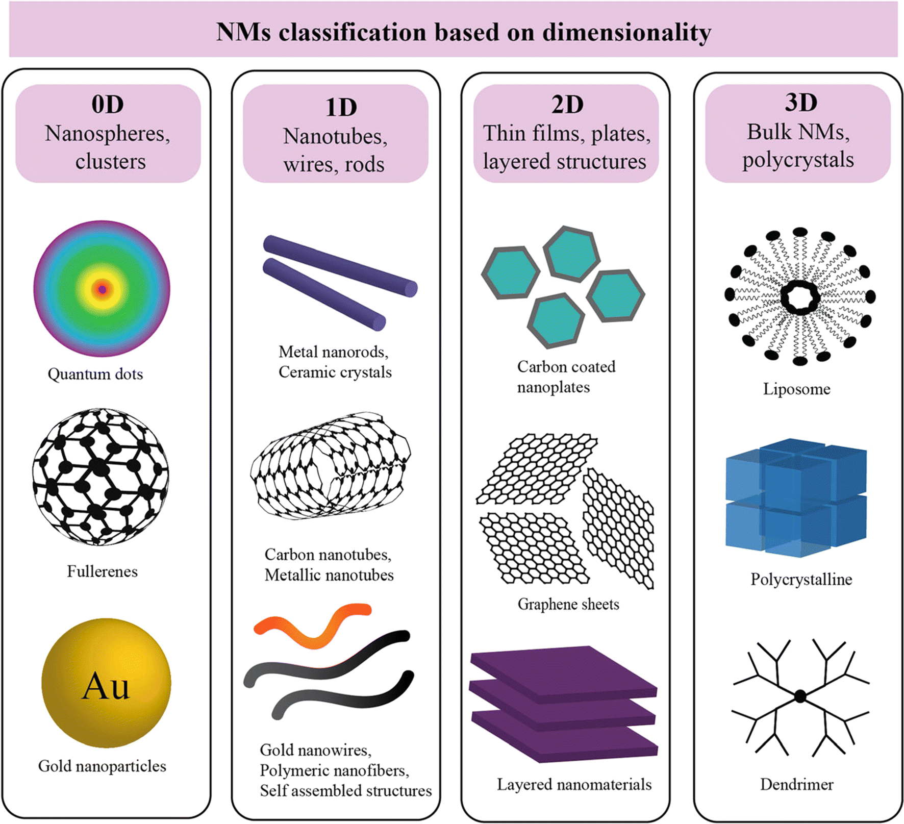 | ||
| Fig. 1 Schematic of nanoparticles by dimensionality with examples: 0D (nanoparticles), 1D (nanorods), 2D (films), and 3D nanocomposites, where synergistic properties emerge from distinct materials combined at the nanoscale.57 | ||
3.2.1.1. Zero-dimensional (0D) NMs. Zero-dimensional NMs refer to nanostructures where all three external dimensions are confined to the nanoscale. This includes: (1) quantum dots (QDs): quantum dots (e.g., CdSe, InP) are semiconductor nanocrystals typically ranging from 2 to 10 nanometers in diameter.28–30 Their size-dependent electronic properties make them valuable for applications in imaging, solar cells, and displays. (2) Fullerenes: fullerenes, such as C60, are closed-cage carbon molecules with a diameter of approximately 0.7 nanometers.31 These spherical structures exhibit unique electronic and chemical properties, contributing to applications in drug delivery, sensors, and materials science. (3) Nanoparticles (NPs): NPs (e.g., gold and silver) and metal oxide NPs (e.g., Fe2O3, TiO2), generally spherical, have dimensions in the nanoscale, typically between 1 and 100 nanometers. Fig. 2 illustrates a size comparison of NPs with various living and nonliving species. They encompass multiple materials and find applications in catalysis, medicine, and nanocomposite fabrication. (4) Metal clusters: metal clusters consist of a small number of metal atoms aggregated into a nanoscale structure. These clusters exhibit size-dependent electronic and catalytic properties, making them relevant for catalysis and electronic applications.
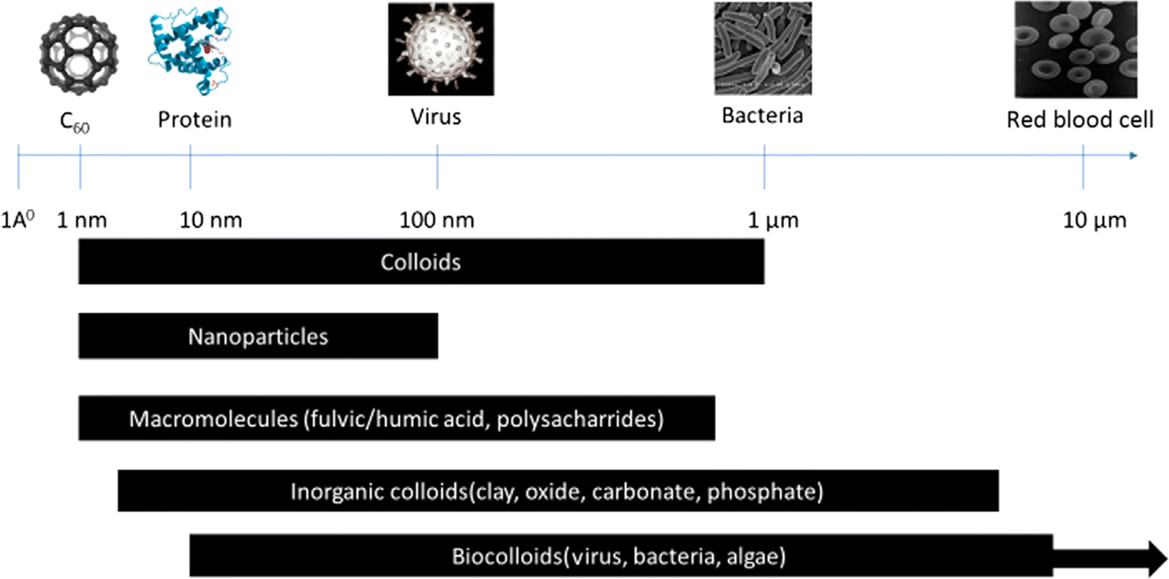 | ||
| Fig. 2 Size comparison of different structures (living and nonliving).58 | ||
3.2.1.2. One-dimensional (1D) NMs. One-dimensional (1D) NMs are characterized by having one dimension at the nanoscale. This category includes a variety of NMs with unique structures and applications: (1) nanowires: nanowires are elongated structures with diameters typically in the range of 1 to 100 nanometers and lengths extending from nanometers to micrometers.32,33 They find applications in electronics, sensors, and nanocomposite materials. (2) Nanotubes: nanotubes, such as carbon nanotubes (CNTs), are hollow cylindrical structures with diameters as small as 0.4 nanometers and lengths ranging from nanometers to millimeters.34 CNTs exhibit exceptional mechanical, electrical, and thermal properties, making them valuable in materials science, electronics, and nanocomposite development.35–37 (3) Nanorods: nanorods are rod-shaped structures with diameters typically ranging from 1 to 100 nanometers and lengths extending up to micrometers.38,39 They are employed in various applications, including catalysis, sensors, and biomedical devices.40,41 (4) Nanofibers: nanofibers are elongated structures with diameters in the nanoscale and varying lengths. They are widely used in tissue engineering, filtration, and electronic devices.42,43
3.2.1.3. Two-dimensional (2D) NMs. Two-dimensional (2D) NMs are characterized by having dimensions in the nanoscale in two directions, forming thin layers or sheets. This category includes various materials with diverse properties and applications: (1) graphene: graphene is a single layer of carbon atoms arranged in a hexagonal lattice with a thickness of approximately 0.34 nanometers.44 It exhibits exceptional electrical conductivity, mechanical strength, and thermal conductivity, making it valuable in electronics, materials science, and energy storage.45 (2) Transition metal dichalcogenides (TMDs): TMDs, such as molybdenum disulfide (MoS2) and tungsten diselenide (WSe2), are layered materials with thicknesses in the nanoscale.46 They possess unique electronic and optical properties, contributing to applications in electronics, optoelectronics, and catalysis.47 (3) Hexagonal boron nitride (h-BN): h-BN is a two-dimensional material with a hexagonal lattice structure similar to graphene. It is an insulator with high thermal conductivity, finding applications in electronics, thermal management, and lubrication.48,49 (4) Black phosphorus (BP): BP is a layered material with a thickness varying in the nanoscale. It exhibits a tunable bandgap, making it suitable for applications in electronics, photodetectors, and energy storage.50,51
3.2.1.4. Three-dimensional (3D) NMs. Three-dimensional (3D) NMs are characterized by nanostructures with nanoscale dimensions in all three directions, resulting in complex 3D architectures. This category includes various materials with distinct properties and applications: (1) nanocomposites: nanocomposites consist of NPs dispersed within a three-dimensional matrix. The size of the NPs and their distribution within the matrix are critical factors influencing the properties of the nanocomposite material.52,53 Applications include lightweight structural materials and advanced coatings. (2) Nanoarchitectures: nanoarchitectures involve the deliberate design and construction of three-dimensional nanoscale structures with precise control over their dimensions and configurations. These structures find applications in drug delivery, catalysis, and energy storage.54 (3) 3D nanoporous materials: nanoscale pores are distributed in three dimensions, offering high surface area and unique adsorption properties. Applications include gas storage, separation, and catalysis. (4) 3D nanowire networks: Networks formed by interconnected nanowires in three dimensions, providing enhanced electrical and mechanical properties.55,56 These networks are utilized in electronics, sensors, and energy devices.
 | ||
| Fig. 3 Various configurations of organic and inorganic nanomaterials.60 | ||
4. Nanomaterial (NMs) used in nanosensors
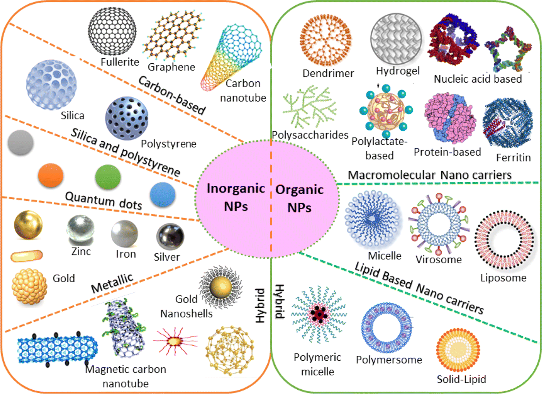
The present section discusses the NMs that have been extensively used in nanosensors. Based on their chemical nature, NMs can be classified, as shown in Fig. 5. The two main categories are inorganic and organic NMs.67 The organic ones are NMs synthesized from proteins, phospholipids, polymers, and hybrids. This group of NMs includes polymers, dendrimers, and liposomes. On the other hand, metals and alloys, metal oxides, semiconductor oxides, composites, and carbon structures are classified as organic. Also, the motivation to create intricate devices encompassing nanoscale materials, biological components, and advanced materials, collectively known as nano biosensors, stems from the growing need to detect a diverse array of molecules at low concentrations with high specificity. For the design and fabrication of nanosensors based on NMs, the key is the creation of sophisticated NMs with regulated functionality, directed size, shape, nature, and crystallinity. The frequently used NMs for this purpose are introduced in the following subsection, which discusses their structures and properties. | ||
| Fig. 5 Classifications of nanomaterials based on chemical nature.68 | ||
4.1. Carbon-based nanomaterials (NMs)
The remarkable features and impressive applications of carbon-based nanomaterials (CBNs), including carbon nanotubes, graphene, fullerenes, and carbon fibers, have made them extremely popular. These CBNs are highly flexible, highly conductive, highly mechanically strong, and have great electron mobility with anisotropic heat conductivity.69,70 Moreover, CBNs introduce excellent stability and minimal toxicity that are environmentally friendly due to their construction of pure carbon.71 Because of their extraordinarily high mechanical, thermal, optical, electrical, and magnetic capabilities, these CBNs are regarded as key components of advanced nanotechnology and smart NMs. These could be used in several industries, including biomedical applications, solar cells, sensors, optoelectronics, medication delivery, environmental monitoring, energy storage devices, and catalysis.Within the fullerene family, C60 stands out as the most significant member. Comprising 20 hexagons and 12 pentagons, it boasts 32 surfaces and 60 vertices. Resembling a soccer ball, its iconic spherical shape has earned it the renowned name “buckyball,” depicted schematically in Fig. 1.73 Also, there are other fullerene structures, such as C70, C76, and C78, which are larger than C60, while C28 and C36 have relatively smaller structures. Fullerene is classified as 0D material, which has a face-centered cubic (FCC) lattice structure, and its type of crystal planes are 111 and 200 at room temperature.74 At elevated temperatures above 677 °C, the FCC is transformed into a graphite-like arrangement.
Additionally, SWNT can exhibit metallic or semiconducting behavior, depending on the diameter and chiral angle.79 CNTs can carry high current without high heating effects because they possess an anisotropic dielectric property.75 CNTs are preferred for sensing the application of gases with low energy consumption due to their high efficiency in detecting gases at room temperature without the need for elevated temperatures. Catalyzed chemical vapor deposition (CVD),80 laser method,81 and arc plasma82 are the most widely used methods for CNTs synthesis. The insolubility, as well as the tendency to agglomerate, are the main disadvantages of CNTs.
Moreover, graphene is the basic building block for other CBNs as it can be wrapped up into 0D fullerenes, rolled into 1D nanotubes, or stacked into 3D graphite. Initially isolated through mechanical exfoliation using the method of “scotch tape,” graphene can be prepared using various techniques. Sonicating the graphite intercalation compounds in surfactants or stabilizers is a form of the “top-down” approach for graphene production.88,89 Also, graphite and its derivatives can be utilized to produce graphene by liquid phase exfoliation90,91 or electrochemical exfoliation in the case of graphite anode with the aid of ionic liquid.92,93 In addition, graphene can be produced from hydrocarbons by the chemical vapor deposition process.94 At the same time, epitaxial growth is employed for the production of graphene on metal surfaces95,96 along with the sublimation of silicon carbide (SiC) in ultrahigh vacuum to produce the hexagonal lattice arrangement of carbon on the SiC substrate after the desorption of Si.97,98 An essential feature of graphene and CNTs that has been exploited in numerous types of nanosensors, especially pollution detection sensors, is the easy transfer of electrons between electroactive species and electrodes.
 | ||
| Fig. 6 Images of (a) nanocrystalline and (b) ultra-nanocrystalline diamond using the scanning electron micrograph.107 | ||
Nanodiamonds possess exceptional mechanical and optical properties, substantial surface areas, and adjustable surface structures. Additionally, they are non-toxic, rendering them highly suitable for biomedical applications, particularly biosensors.108,109 These nanodiamonds have been synthesized through various methods, including the detonation technique,110 plasma-enhanced chemical vapor deposition (CVD),111 graphite ion irradiation,112 high-energy ball milling of high-pressure high-temperature (HPHT) diamond microcrystals,113 and laser ablation.114
Many methods, including X-ray photoelectron spectroscopy (XPS),123,124 laser scanning microscopy,125 Raman spectroscopy,126,127 energy dispersive spectroscopy (EDS), transmission electron microscopy (TEM),128 scanning electron microscopy (SEM),129 atomic force microscopy (AFM), optical microscopy, as well as conductivity measurements and electrochemistry, have been used for characterizing CBNs. Fig. 7 shows the dimensionality of some carbon allotropes.
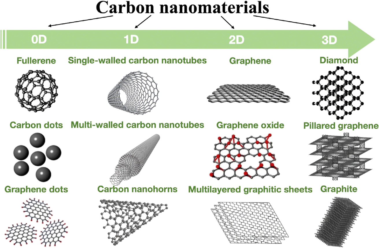 | ||
| Fig. 7 Dimensionality of various allotropes of carbon.130 | ||
4.2. Metal-based nanomaterials (NMs)
The ability to generate metal NPs within the range of 1 to 100 nm has resulted in numerous applications in nanosensor research. These NPs possess distinct characteristics, such as a high surface concentration of atoms/molecules and a significant surface-to-volume ratio. These can be harnessed to enhance detection and sensing in food-packing industries and healthcare-related disciplines. Metal NPs can be utilized independently or in conjunction with other nanostructures, amplifying signals, increasing sensitivity, and achieving substantial advancements in the nanosensors industry. The involvement of metallic NPs in biological and chemical sensing is closely tied to their physicochemical properties.131Noble metals characterized by their high oxidation and corrosion resistance at high temperatures, namely platinum (Pt), silver (Ag), gold (Au), palladium (Pd), and ruthenium (Ru) NPs, have gained significant popularity and have been subjected to extensive research. Although these noble metals exhibit chemical inactivity in their macroscopic state, they exhibit distinctive physiochemical characteristics at the nanoscale.132
The categorization of noble metals NPs synthesis methodologies comprises two main approaches: “bottom-up” and “top-down”. Physical manipulation techniques such as pyrolysis, lithography, and micro-patterning are the core of the top-down approaches. At the same time, the bottom-up methods employ chemical transformations, including microwave synthesis, microemulsion techniques, and chemical reduction.133 Each method has its advantages and disadvantages. Top-down methods permit large-scale production without the need for chemical purification. However, the resulting NPs exhibit a wider range of sizes and varying morphologies, besides the difficulty of controlling synthesis parameters.
Conversely, a specific morphology and size, as well as easy control of the parameters, can be achieved by bottom-up methods. Still, it is not easy to attain large-scale production. Also, the bottom-up approaches are cheaper than the top-down ones.134
Conversely, the drawbacks encompass high energy consumption and cost, low productivity, reduced thermal stability, and substantial waste generation. Chemical methods involve plasma CVD, hydrothermal, polyol synthesis, pyrolysis, and the sol–gel process. These techniques necessitate the presence of metal precursors, stabilizing or capping agents, and reducing agents. The recognized precursors include PtCl2, Pt(NH3)4(NO3)2, and H2PtCl6, while the frequently employed reducing agents to control the size and shape of the NPs are ascorbate, trisodium, potassium bitartrate, and sodium borohydride.140 In addition, the biosynthetic pathway was employed using different plant extracts, such as those from Pinus resinosa and Ocimum sanctum, to synthesize platinum NPs biologically. The biosynthetic pathway has several benefits, including cost-reduction, tiny size (3–5 nm), non-toxicity, environmental friendliness, and quick synthesis. Still, it suffers from the difficulty of controlling the shape and size of the NPs. Various techniques can be utilized to characterize platinum NPs, such as TEM, XRD, SEM, and FTIR.
The numerous benefits associated with the distinct chemical and physical characteristics of metal NPs, further supported by their nanoscale size, explain their extensive use in nanosensors. Recently, noble metal NPs incorporated with carbon nanotubes (CNTs) have formed a novel type of composite materials. These materials effectively combine the distinct properties of noble metal NPs and CNTs, resulting in new functionalities arising from the cooperative effects between the two components. Consequently, noble metal NPs/CNTs nanohybrids have demonstrated remarkable potential in various fields, with particular emphasis on chemo/biosensors.132 For example, when silver NPs were used for immobilized graphene oxide (GO), colloidal carbon was coated on the NPs to improve their biocompatibility and eliminate toxicity.142
Also, cerium oxide NPs (CeO2 NPs) play a significant role as oxidative catalysts, in addition to their use in chemical and humidity sensors.148 In contrast, chromium oxide NPs (Cr2O3 NPs) are used for electrochemical and strain sensing.149,150 These materials are cost-effective and stable, making them suitable for many intriguing applications. While most research on metal oxides has traditionally focused on industrial catalysis and ceramics, investigations into their interaction with biomolecules have also been explored. Numerous compelling sensors and biosensors involving different metal oxide NPs have emerged in recent years. The shape and size of various metal oxide NPs, as appeared under TEM, are shown in Fig. 8.151
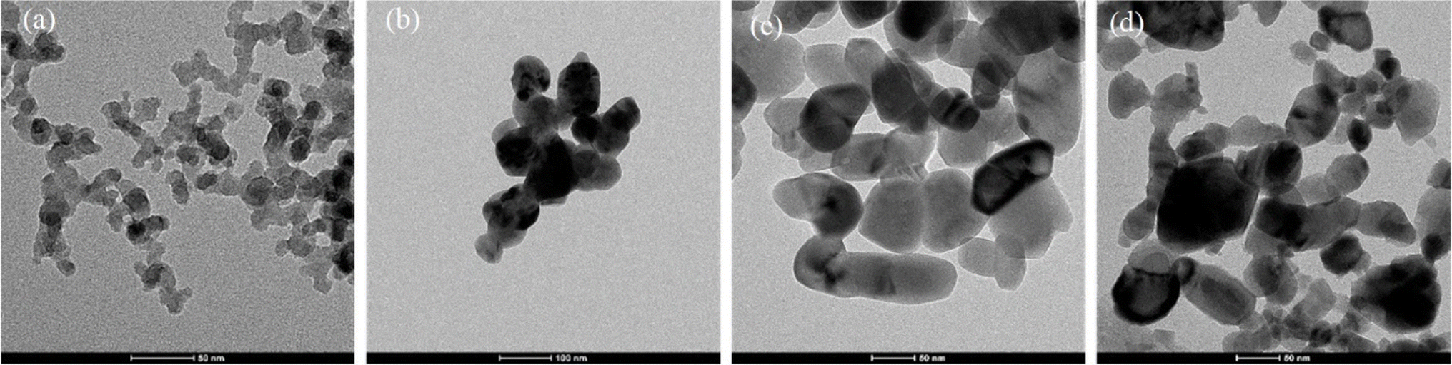 | ||
| Fig. 8 TEM images of metal oxides' nanoparticles: (a) (Al), (b) (Cu), (c) (Ti), (d) (Zn).151 | ||
4.3. Silicon-based nanomaterials (NMs)
Since silicon-based NMs have favorable biocompatibility, surface tailorability, excellent electrical, optical, and mechanical properties, and compatibility with conventional silicon technology, they are an essential class of NMs widely investigated.152–154 In particular, silicon nanowires (SiNWs) have demonstrated significant promise for various uses in sensors and bioimaging.155,156 SiNWs and SiNWs arrays have also been utilized recently to track environmental pollution. Three electrodes comprise the conventional field effect transistor (FET)-based silicon nanowire (SiNW) biosensor. Their charge density variation, which causes variations in the electric field at the SiNW's outside surface, is the mechanism underlying their sensing process.Moreover, SiNW's exceptional qualities, including their tunable optical and electrical characteristics, high surface-to-volume ratio, and biocompatibility, made them attractive for viruses and metal ion detection sensors. Moreover, SiNWs-based electrochemical sensors can be enhanced to be available for quick and accurate pesticide detection. Bottom-up157 and top-down158,159 approaches are the most frequently used methods for the nanofabrication of SiNWs. SiNWs grow from a substrate in the bottom-up process. In contrast, a silicon-on-insulator fabrication technique is essential in the top-down method.
4.4. Semiconductor quantum dots
Recent developments in semiconductor quantum dots (QDs) and colloidal nanocrystalline semiconductors have demonstrated significant promise for technical and fundamental research applications.160 QDs are the perfect optical labels for sensing because of their unique photophysical characteristics, which include restricted emission bands, strong Stokes shifts, high fluorescence quantum yields, and very low photobleaching.161 Due to their size-controlled luminescent properties, QDs have demonstrated tremendous potential in molecular detection in recent breakthroughs. QDs have been used as optical markers for detecting heavy metal ions by researchers.162–164 One well-researched approach for sensing metal ions, pesticides, hazardous gases, tiny compounds, and industrial effluent uses fluorescent QD sensors.165–168 Chlorpyrifos (CP) and other organo-phosphorothioate pesticides are recognized explicitly by the fluorescence turn-on response, enabling pesticide detection at concentrations as low as 0.1 nM. Significantly, at a limit of 5.5 ppb, the fluorescence turn-on chemosensor can directly identify CP residues in apples.169Due to their distinct size and shape-dependent optical properties, II–VI (CdSe, ZnS), III–V (InAs, InP), and IV–VI (PbS, PbTe) QDs have been researched over the past ten years. However, they are not environmentally friendly due to the inclusion of Pb and Cd elements, which limits their use.170 Thus, research into QDs with less hazardous and environmentally favorable components is necessary. In order to create less hazardous QDs with comparable exceptional optical qualities, I–III–VI ternary QDs are created by substituting one monovalent and one trivalent cation for the divalent cation found in II–VI binary QDs.171 The primary reasons for the increased interest in ternary I–III–VI QDs are their appealing optical and electrical characteristics, low toxicity, and environmental friendliness, providing a safer option than II–VI and IV–VI QDs.172 This makes them popular for biocompatible solar cell applications, water treatment, biological applications, and heavy metal ion detectors in water.171 These materials are considered one of the most recent varieties of QDs to be found and used in environmental and biological monitoring disciplines.
5. Sensing mechanisms of nanomaterials
NMs possess unique properties arising from their high surface-to-volume ratio, quantum confinement effects, and tailorable surface chemistry, making them attractive for sensing applications across various fields. The sensing mechanisms employed by NMs can be broadly categorized into optical, electrochemical, and other transduction principles, depending on the nanomaterial and the analyte of interest. Table 1 shows a range of nanomaterial sensors using different detection methods for highly sensitive analyte detection.| Nanomaterial | Detection mechanism | Analyte | Detection range | Detection limit | Reference |
|---|---|---|---|---|---|
| Graphene quantum dots (GQDs) and acid-functionalized multiwall carbon nanotubes (MWCNTs) | Electrochemical | Dopamine | 0.25–250 μM | 95 nM | 180 |
| Gold and silver nanoparticles | Colorimetric sensing platform | Target DNAs and target proteins (thrombin and platelet-derived growth factor) | 15–40 nM | 19 nM | 181 |
| Graphene | Prism-coupled surface plasmon resonance (SPR) biosensor | Glucose | 25–175 mg dl−1 | — | 182 |
| Quantum dots | Electrochemiluminescence (ECL) | Alpha-fetoprotein (AFP) and carcinoembryonic antigen (CEA) | 0.001–0.1 pg mL−1 | 0.4 fg mL−1 | 183 |
| Graphene oxide | Fluorescent aptasensor | Aflatoxin B1 | 0 ng mL−1 - 3 ng mL−1 | 0.25 ng mL−1 | 184 |
| Silica nanoparticles | pH-responsive fluorescent | pH | pH 5.5 to 9.0 | — | 185 |
| Chitosan, graphene, and titanium dioxide (CS/RGO/TiO2) | Electrochemical sensing | Lead ions (Pb2+) | 1 ng L−1 to 1000 ng L−1 | 0.33 ng L−1 | 186 |
| Titanium dioxide nanotubes (TNTs) and silver nanoparticles (AgNPs) | Electrochemical biosensing | Heat shock protein 70 (HSP70) | 0.1 to 100 ng mL−1 | 0.48 ng mL−1 | 187 |
5.1 Optical sensing mechanisms
- Localized Surface Plasmon Resonance (LSPR): noble metal nanoparticles, such as gold and silver, exhibit LSPR, which is the collective oscillation of conduction electrons induced by incident light. The LSPR frequency is highly sensitive to changes in the local dielectric environment, enabling the detection of analytes through shifts in the LSPR peak wavelength or intensity changes. Mayer and Hafner173 comprehensively reviewed recent advancements in localized LSPR, highlighting its significance in detecting molecular interactions near noble metal nanostructures. Their overview of LSPR sensing strategies, mainly focusing on metal nanoparticle-based sensors for label-free detection in biological applications, sheds light on the evolving landscape of LSPR technology and clarifies inconsistencies in nomenclature within the field.- Fluorescence quenching or enhancement: semiconductor quantum dots exhibit size-dependent fluorescence properties, which the presence of analytes can modulate through quenching or enhancement mechanisms. Analyte binding or interaction with the quantum dot surface can alter the fluorescence intensity or lifetime, enabling sensitive detection. For instance, Das et al.174 studied the mechanism of fluorescence enhancement and quenching effect of single-walled carbon nanotubes (SWCNTs) on highly fluorescent graphene quantum dots (GQDs) over a wide range of SWCNT concentrations. At very low SWCNT concentrations, the fluorescence intensity of GQDs was enhanced. In contrast, systematic fluorescence quenching was observed at higher concentrations due to a combination of dynamic and static quenching, offering insights into fluorescence tuning for bio-imaging and drug delivery applications.
- Surface-enhanced Raman scattering (SERS): the SERS technique, renowned for its capability to detect molecular signatures through vibrational bonding information from Stokes shifted scattered photons, has found diverse applications in ultra-sensitive chemical sensing across various fields such as the food industry, explosive detection, forensic science, microbiology, medicine, and biomedical diagnostics, owing to its high detection sensitivity and the development of nanofabrication techniques leading to molecular detection limits down to single molecules, with plasmonic substrates being a major focus for such advancements. Plasmonic nanostructures, such as metal nanoparticles or nanostructured surfaces, can enhance the Raman scattering signal of analytes adsorbed on their surfaces by several orders of magnitude. This enhancement enables the detection of low concentrations of analytes through their unique Raman fingerprints. Recently, Mandal and Tewari175 provided a comprehensive review that primarily focuses on the progress made in SERS over the last 20 years, emphasizing SERS substrate fabrication techniques and chemical sensing, with additional discussions on its applications in food safety, food, and fuel adulteration, forensic science, defense, biology, and biomedical diagnostics.
5.2 Electrochemical sensing mechanisms
- Electrical conductivity changes: carbon nanotubes, graphene, and other conductive NMs can exhibit changes in their electrical conductivity upon adsorption or interaction with analytes. These changes can be measured and correlated with the analyte concentration, enabling the development of chemical sensors and biosensors. For instance, Li et al.176 investigated the development of a simple, reliable, and reproducible single-walled carbon nanotube (SWNT) sensor platform for gas and organic vapor detection at room temperature. The study demonstrated well-defined and reproducible linear electrical responses with a detection limit of less than 44 ppb for NO2 and 262 ppb for nitrotoluene. Moreover, Shooshtari et al.177 investigated the effect of humidity on the electrical conductivity of vertically aligned carbon nanotube (CNT)-based gas sensors designed for volatile organic compound detection. The study found that an increase in relative humidity from 10% to 80% resulted in a 4% reduction in sensor conductivity, while conductivity slightly increased above 80% humidity.- Catalytic properties: metal nanoparticles, such as platinum, palladium, and gold, possess catalytic properties that can facilitate electrochemical reactions involving analytes. The presence and concentration of analytes can be determined by monitoring the electrochemical response, such as current or potential changes. For instance, Zhou et al.178 developed a novel electrochemical sensor for formaldehyde detection by depositing nanostructured platinum-palladium alloy onto a Nafion-coated glassy carbon electrode. This sensor demonstrated remarkable electrocatalytic activity, with a linear detection range of 10 μM to 1 mM and a low detection limit of 3 μM in acidic solution, showing promise for various applications.
- Ion-gating effects: transistor-based sensors employing semiconducting NMs, such as carbon nanotubes or metal oxide nanostructures, can leverage ion-gating effects. The binding of charged analytes to the nanomaterial surface can modulate the electrical properties, enabling the detection of various ionic or charged species. Subramanian et al.179 investigated the potential of titanium dioxide (TiO2) for next-generation transistors, particularly ion-gated transistors (IGTs). In their work, TiO2 films were fabricated through a wet chemical approach, demonstrating transistor behavior with room temperature ionic liquids, aqueous electrolytes, and pH sensing capability in TiO2 IGTs, boasting a ∼48 mV pH−1 sensitivity. Furthermore, they showcased the viability of low-temperature, solution-processed TiO2-based IGTs on flexible PET substrates, which exhibited stability even under moderate tensile bending.
5.3 Other sensing mechanisms
- Mechanical transduction: NMs can be incorporated into mechanical transducers, such as cantilevers or resonators, where the mass or surface stress changes induced by analyte binding can be detected through shifts in resonance frequency or cantilever deflection.- Magnetic property changes: magnetic nanoparticles, such as iron oxide or ferrite nanoparticles, can change their magnetic properties upon interaction with analytes. These changes can be measured using magnetic sensors or techniques like magnetic resonance imaging (MRI).
- Thermal or calorimetric effects: some NMs can exhibit thermal or calorimetric responses upon binding or reacting with analytes. By monitoring temperature changes or heat flow, the presence and concentration of analytes can be determined.
It is worth noting that the choice of sensing mechanism and the specific nanomaterial employed depends on the target analyte, the desired sensitivity and selectivity, and the application requirements. Researchers often combine various NMs and sensing mechanisms to develop robust and versatile sensing platforms tailored to specific analytical needs.
6. Application of nanomaterial-based nanosensors
6.1. Overview
Nanosensors have numerous advantages over traditional sensors made from bulk materials. Their sensitivity and specificity are enhanced due to unique physicochemical characteristics at the nanoscale. NMs' high surface-to-volume ratio and novel properties, such as nanophotonics, enable increased sensitivity and specific detection. Moreover, nanosensors offer cost and response time advantages, making them suitable for high-throughput applications. They provide real-time monitoring compared to conventional methods like chromatography or spectroscopy, which can be time-consuming and require extensive sample preparation. With applications in healthcare monitoring, environmental monitoring, and various other fields, nanosensors are paving the way for advancements in personalized medicine, disease detection, and scientific research, as shown in Table 2.1,68,188–191| Nanosensors | Property | References |
|---|---|---|
| Carbon nanotubes (CNTs) | Highlighted for their high electron transferability, extensive level of detection, ability to stabilize enzymes, and sensitivity to degradation by white blood cells | 192–194 |
| Graphene quantum dots | Noted for improving the surface and electrochemical properties of sensors when combined with other nanostructures | 195 and 196 |
| Magnetic NPs | Discussed their ability to enhance catalytic properties and glucose detection due to the activity of enzyme glucose oxidase when bound to copper. They are also mentioned for their magnetic reusability and selectivity | 197–199 |
| Nano optical sensor | Mentioned for their role in noninvasive glucose monitoring and the modulation of release rates in response to abdominal deformities | 200 and 201 |
| Electrochemical biosensors | Characterized by the ability to quantify two different mechanisms of ion exchange within the sensor and their contribution to the diversity of biosensor fabrication | 202 and 203 |
| Visual nanosensor | Described as the most advanced type, with a small volume yet powerful detection capabilities and their ability to function optimally even with low concentrations of analytes | 204–206 |
6.2. Application of nanomaterial-based nanosensors in healthcare
Nanomaterial-infused nanosensors have emerged as a pivotal innovation in healthcare and biomedical fields, demonstrating remarkable proficiency in identifying tumor-specific biomarkers, circulating tumor cells, and extracellular vesicles discharged by tumors. This capability facilitates intelligent cancer detection, significantly enhancing patient prognosis.207 An array of NMs, including gold nanoparticles, quantum dots, polymer nanoparticles, carbon-based NMs, and metal/metal oxide nanoparticles, has been rigorously explored for their potential in biosensing endeavors.208 Moreover, the advent of nanomaterial-based flexible sensors (NMFSs) represents a significant leap forward. These sensors, capable of adhesion to human skin or incorporation into garments, are designed to track physiological metrics and furnish vital medical insights.209 Specifically, carbon-based NMs such as carbon nanotubes, graphene, carbon quantum dots, and carbon fibers have been employed as sensor elements for biomarker detection.In contrast, other materials, such as biodegradable silk nanofibers, have been employed to harvest energy to power these sensors.210 These materials are distinguished by their high surface-to-volume ratio, exceptional electrical conductivity, and compatibility with biological systems.211 Collectively, these advancements underscore the transformative impact of NMs in the biosensor domain, enabling swift and accurate detection, continuous health monitoring, enhanced sensitivity, and cost-efficiency in healthcare and biomedical applications.212
In the study presented in Fig. 9 by M. Iarossi et al.,213 the team innovatively crafted a surface-enhanced Raman spectroscopy (SERS) active interface using an array of gold nanopyramids (Au NPs) equipped with plasmonic tips. This cutting-edge technique was designed to observe cellular activities and effectively distinguish between undifferentiated and differentiated neurons through the application of principal component analysis. The gold nanopyramids, characterized by tip curvatures measuring 10 nm and exhibiting localized plasmon resonance at a wavelength of 785 nm, were utilized to examine ND7/23 neurons non-invasively. The collection of SERS spectra from cells situated on these gold nanopyramids, conducted with a Raman spectrometer, unveiled the presence of critical cellular components such as membrane constituents, proteins, lipids, and nucleic acids like DNA and RNA. Following the SERS analysis, a cell viability test confirmed that the majority of the cells remained viable, with only a minimal number of them perishing on the gold nanoparticle arrays placed atop glass surfaces.
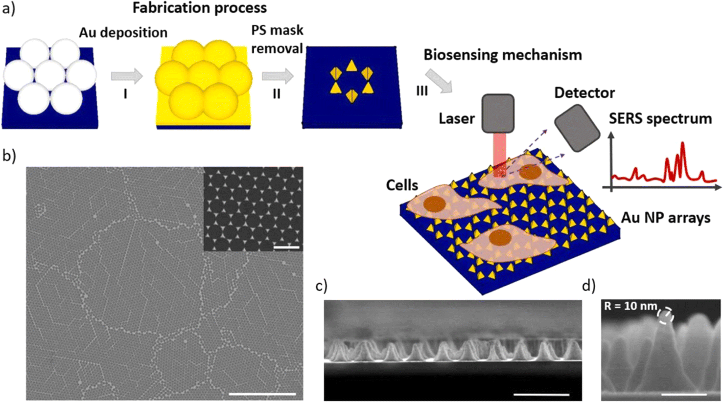 | ||
| Fig. 9 Illustrates (a) the construction sequence of the gold nanoparticle (Au NP) array on glass, serving as an SERS platform to investigate cellular activities. This process involves assembling a colloidal mask, depositing gold, and then removing the nanospheres. Subsequently, the Au NP arrays function as a SERS foundation for tracking the amplified Raman signals of neurons throughout various phases of their differentiation. (b) A scanning electron microscope (SEM) image displays the extensive layout of the Au NP array (scale bar: 10 μm), with an inset providing a closer look at the Au NPs to showcase their periodic arrangement (scale bar: 500 nm). (c) A cross-sectional SEM view reveals the vertical structure of these nanoforms (scale bar: 500 nm). (d) An enhanced view of the cross-section SEM image of an individual Au NP, emphasizing the acuteness of its tip, which measures 10 nm in curvature (scale bar: 100 nm).213,214 | ||
M. K. Hameed et al.215 developed anisotropic gold nanostars (AuNS) by utilizing varying amounts of silver nitrate (AgNO3) to guide their shape, thereby adjusting the length of the spikes on the nanostars. The uptake of these AuNS by MDA-MB-231 breast cancer cells was notably more effective than in normal cells, showcasing their promise as carriers for cancer treatment drugs. The shape of the AuNS was determined by the levels of gold(III) chloride and the AgNO3 additive, with the nanostars formed without the use of surfactants displaying distinct characteristics from those synthesized with surfactants. Confocal microscopy images provided evidence of the AuNS being absorbed by the cancer cells, marked by strong blue fluorescence within the nuclei and green fluorescence in the cytoplasm. This research underscores the critical role of nano spike morphology in enhancing the SERS analysis of cell components, underlining its potential benefits in biomedical applications.
The vigilant surveillance of glucose concentrations within the urine is paramount, as heightened levels are harbingers of diabetes mellitus progression. A urinalysis yielding a positive outcome signifies that the glucose concentrations within the organism surpass the threshold of 50–100 mg dL−1 (equivalent to 2.78–5.55 mM). The pioneering glucose meter for urine in Japan unveiled in 1996, demonstrated commendable proficiency in monitoring glucose concentrations spanning from 0 to 500 mg dL−1. Subsequently, in 1999, the TOTO Corporation spearheaded the innovation of a glucose monitoring device seamlessly integrated into toilet seats, thereby facilitating the analysis of diluted urine specimens, as depicted in Fig. 10. Further, the exploration into carbon nanotubes (CNTs) for the detection of glucose in urine has been noteworthy. The strategic employment of CNTs dissolved in an aqueous solution of the biopolymer chitosan (CS) has enabled precise glucose measurements in urine, devoid of any interference, with a detection threshold reaching as low as 3 M.216
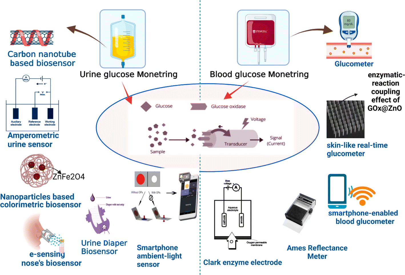 | ||
| Fig. 10 Diagnosis of glucose level in urine and blood with the help of modern biosensor tools.214,216 | ||
T. Patil et al.217 highlighted the distinctive physicochemical characteristics of gold nanoparticles (AuNPs), noting their potential in various biological contexts. Various synthesis techniques, including biologically based ones, can produce AuNPs. The surface functionalization process grants these nanoparticles colloidal stability, broadening their utility in water-based and physiological settings. Particularly, the surface plasmon resonance (SPR) feature of AuNPs is leveraged in developing biosensing and bioimaging tools for diagnostic purposes and pathogen identification. Applications of functionalized AuNPs span bioimaging, biosensing, cancer treatment, drug delivery, hyperthermia treatment, and fighting microbial infections. There is, however, a call for more research into the attachment of biomolecules to the nanoparticle surface to refine the use of AuNP-based diagnostic technologies. Additionally, the issue of how these nanoparticles are cleared from the kidneys in live-body medical applications presents a significant challenge that needs further investigation.
6.3. Application of nanomaterial-based nanosensors in environmental monitoring
Y. Shimizu et al.223 conducted a study on the SO2 detection capabilities of various semiconductor metal oxides, identifying WO3 as having the highest sensitivity at 400 °C. They discovered that incorporating 1.0 wt% Ag notably enhanced this sensitivity at 450 °C. This improvement is attributed to changes in the surface states of SO2-related adsorbates and the electronic interactions between the adsorbates and WO3. The study highlights how adding noble metals to WO3 can significantly improve its ability to sense SO2, making it highly applicable in environmental monitoring systems to detect sulfur dioxide concentrations in the atmosphere. Such sensors are particularly valuable in industrial settings, power generation plants, and other operations where it is essential to monitor and control SO2 emissions to safeguard environmental quality and public health. Moreover, these enhanced sensors can be incorporated into air quality monitoring networks, offering timely and accurate data on pollution levels.
Q. Wang et al.224 synthesized the gas-sensing properties of In–Sn oxides composites by hydrothermal method. This study explores the successful synthesis of nanoparticles using an environmentally friendly approach and investigates their gas-sensing performances towards ethanol. The findings contribute to developing advanced materials for gas sensors with improved sensitivity and selectivity, which are crucial for various industrial and environmental monitoring applications.
6.4 Application of nanomaterial-based nanosensors in industries
One of the main advantages of nanosensors is that they offer precise detection capabilities for sensing physical parameters, CBRN (chemical, biological, radiological, and nuclear) agents, and more. Additionally, nanosensors are tiny and portable, making them suitable for high-throughput applications. In industries, nanosensors can be integrated with nanoelectronics to add native processing capability, enabling real-time monitoring and control. For example, nanosensors can detect product defects early in manufacturing processes, allowing for adjustments before large quantities are produced.1,68,189,221,225 This not only saves time but also reduces costs.
Furthermore, nanosensors have significant applications in the aerospace and defense industries. In aerospace applications, they enable real-time structural monitoring to ensure the integrity of aircraft components and minimize maintenance costs. Nanosensors also improve fuel efficiency and flight safety while reducing environmental impact.
In the defense sector, nanosensors offer advanced threat detection and surveillance capabilities. They can detect CBRN threats, providing crucial situational awareness and protecting military personnel. Additionally, nanosensors find applications in explosive detection, camouflage technology, and unmanned aerial vehicles (UAVs) for surveillance.
Moreover, nanosensors can be used for environmental monitoring in industries such as water quality assessment. By effectively identifying chemicals and bacteria that threaten aquatic life and human health, these sensors ensure the safety of water resources.1,68,189,221,225
In industries, nanosensors have proven to be invaluable tools. They can be used to monitor the quality of food and pharmaceuticals, ensuring that they meet the required standards. Additionally, nanosensors are crucial in safeguarding workers in dangerous work settings by detecting potential hazards.
One of the key advantages of nanosensors in industries is their ability to enhance efficiency while reducing costs and minimizing waste. For example, in manufacturing, nanosensors can detect product defects early, allowing adjustments to be made before large quantities are produced.1,68,189,221,225 This not only saves time but also saves companies money.
A remarkable development in nanosensors is the creation of self-powered nanosensors called triboelectric nanosensors (TENS). These sensors use an array of mercury-sensitive tellurium nanowires to detect trace amounts of mercury ions in water or food and provide instant reports on their presence. This breakthrough demonstrates the potential of nanosensors in monitoring processes and ensuring product safety.
In the electronics industry, the integration of nanosensors is transforming the field. These sensors offer enhanced precision, sensitivity, and functionality for consumer electronics, communication devices, and smart systems. Nanosensors enable faster data processing, improved energy efficiency, and miniaturization of electronic components, paving the way for advanced devices and technologies.
Moreover, in the manufacturing sector specifically, nanosensors play a vital role in quality control and process optimization. They enable real-time monitoring of production parameters to ensure optimal performance and cost-effectiveness. Nanosensors also contribute to developing smart factories and implementing Industry 4.0 principles, increasing productivity and efficiency.1,68,189,221,225
6.5 Application of nanomaterial-based nanosensors in security and defense
In the fields of forensics, environmental monitoring, and the production and storage of explosives, the ability to detect minute quantities of explosives is crucial. The threat that explosives pose to both national and global security remains significant. Recent incidents have highlighted the essential role of explosive trace detection (ETD) technologies.226 The use of homemade explosives (HMEs) in terrorist activities is especially concerning due to their high potential for destruction, the ease of acquiring materials, and the availability of online instructions for their creation and use. Therefore, improving current ETD techniques and continuously exploring new methods is critical.Explosives are classified according to their molecular structures and compositional characteristics, as depicted in Fig. 11. The use of nitroaromatic compounds, such as TNT (trinitrotoluene) and DNT (dinitrotoluene), in ammunition raises environmental concerns.227 Organic peroxides, which are notably sensitive to heat, shock, and friction, are commonly used in the making of homemade explosives (HMEs). Nitrate esters, typically liquid, are employed in the military for purposes such as plastic explosives, detonators, and propellants. Ammonium nitrate/fuel oil (ANFO) mixtures and urea nitrate (UN) are among the most frequently used materials for crafting improvised explosive devices (IEDs).
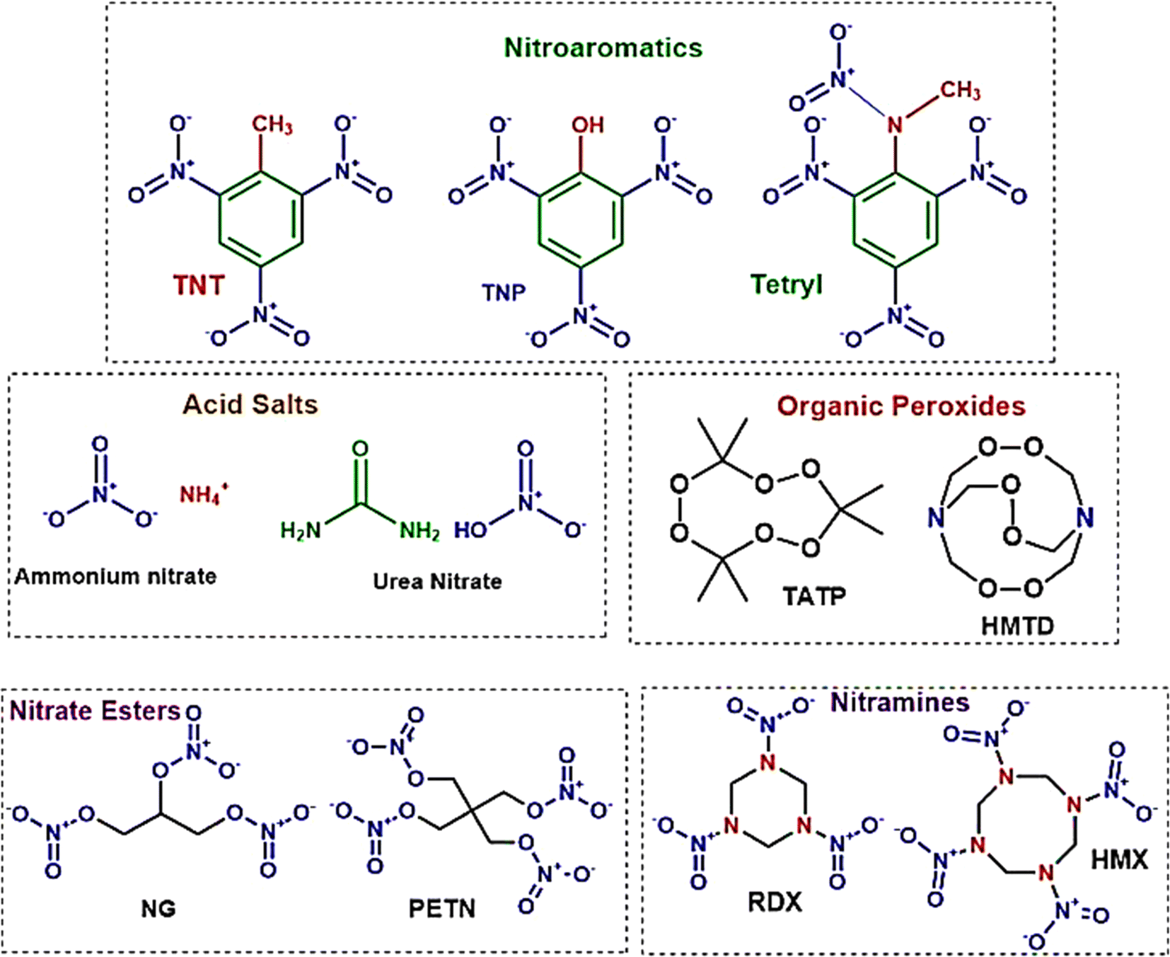 | ||
| Fig. 11 Provides a systematic categorization of explosives based on their chemical groupings. This diagram serves as a comprehensive framework for understanding the diverse classifications within the field of explosives, structured according to their distinct chemical compositions.228 | ||
The wide range of chemical and physical attributes of explosives complicates collecting samples and detecting traces of these materials. Typically, particulate sampling is conducted with sampling wands, where the direction, pressure, and method applied are critical to collect samples efficiently. Vapor sampling poses an additional challenge due to many explosives' shallow vapor pressures. Furthermore, the “sticky” nature of numerous explosives causes them to cling to various surfaces, leading to the accumulation of explosive particles and thus reducing the amount of analyte molecules available per sample volume. Examining luggage and cargo, often wrapped in protective materials, presents logistical and operational challenges that can hinder effective sampling. In every instance, there is a risk that non-explosive materials could cause false positive alerts. Therefore, adopting novel detection technologies requires a comprehensive assessment of regulatory (concerning threats, sensitivity, selectivity), operational, civilian, and economic factors.
Investigations and advancements within the NMs sphere have illuminated nanostructured entities' potential to serve as detectors for various chemical and biological substances, including explosives. Developing exceptionally diminutive apparatuses endowed with heightened detection capabilities is a cornerstone of nanosensor technology. Notably, the concepts of electronic noses, nanowire/nanotubes, and nanomechanical systems emerge as the most promising candidates poised to establish effective technological frameworks for identifying trace amounts of explosives. The electronic nose approach endeavors to replicate the olfactory capabilities of bomb-detection canines, albeit devoid of their associated limitations. This innovative device integrates a chemical sensing mechanism, a sample collection module, and a pattern recognition apparatus, typically in the form of an artificial neural network, as shown in Fig. 12, to achieve its function.228
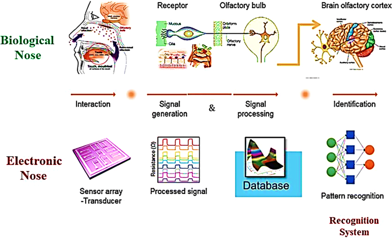 | ||
| Fig. 12 Delineates the concept of the Electronic Nose (E-nose), an innovative diagnostic tool designed to mimic the olfactory system's functionality. This illustration encapsulates the E-nose technology's principle operations and theoretical underpinnings, highlighting its pivotal role in detecting and analyzing complex aromas and chemical signatures.228 | ||
L. D. Bastatas et al.229 designed a chemiresistive sensor to detect ammonium nitrate using silica nano springs coated with zinc oxide (ZnO). This breakthrough leverages the enhanced activation of charge carriers for more efficient desorption of analytes and boosts sensor recyclability through UV light irradiation. J. Qu et al.230 also developed a chemiresistive sensor array to identify various explosives, including TNT, DNT, and TNP. By doping ZnO with metals like cobalt (Co), nickel (Ni), and iron (Fe), they were able to enhance the adsorption of explosive molecules on the metal oxide (MOx) surface, significantly increasing the sensor's sensitivity. These enhancements allowed for detecting explosives at concentrations ranging from parts per billion to parts per trillion, with a rapid response time of just 12 seconds. The enhanced speed of these doped sensors is credited to the reduced distance for charge transfer between the charge reservoir layer and the surface defect centers on the MOx nanoparticles, as demonstrated in Fig. 13.
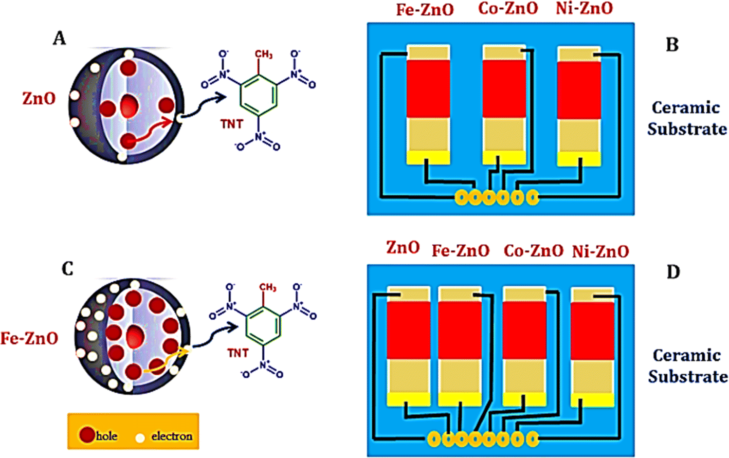 | ||
| Fig. 13 Depicts the Fe-doped ZnO chemiresistive sensor configuration, providing an insightful visualization of the intricacies of charge transfer mechanisms within both undoped and doped ZnO structures (A and C). Furthermore, it offers a schematic overview of a gas sensor array, which integrates three doped sensors—namely Fe–ZnO, Co–ZnO, and Ni–ZnO (B), alongside a comprehensive representation of an expanded array incorporating an additional undoped ZnO sensor, thereby culminating in a four-sensor array that includes ZnO, Fe–ZnO, Co–ZnO, and Ni–ZnO (D). This figure effectively conveys the enhanced detection capabilities facilitated by the strategic incorporation of dopants into ZnO matrices.228 | ||
The development of some MOx (metal oxide) sensors that can function at lower temperatures, as showcased by L. Bastatas and J. Qu, marks a significant improvement, offering potential benefits such as reduced energy consumption and decreased risk of hazards in their application. By adjusting the operational temperature, employing arrays of sensors, and using composite materials, the sensitivity of MOx semiconductors towards specific explosive compounds can be significantly enhanced. The rate at which oxygen is adsorbed onto the surface of MOx changes with temperature variations, allowing for identifying particular gases through the sensor's response. Leveraging data from multiple sensors, each operating at different temperatures can increase selectivity in detecting compounds. Furthermore, composite MOx structures can be custom-designed, selecting component materials specifically for their efficacy in sensing distinct gas analytes, thus refining the detection process.231,232
J. Warmer et al.233 employed sensors based on tin dioxide (SnO2) and tungsten trioxide (WO3) to detect triacetone triperoxide (TATP) and diacetone diperoxide (DADP). By capitalizing on the temperature-dependent oxidative and reductive properties of organic peroxides, they improved the selectivity of WO3 films for TATP through temperature adjustments. The detection threshold for these sensors was determined to be in the parts per billion (ppb) range, showcasing their high sensitivity in identifying these specific explosives.
Z. Yang et al.234 developed an innovative array of Schottky optoelectronic sensors by combining silicon nanowires (SiNWs) with titanium dioxide (TiO2) and reduced graphene oxide, achieving impressive detection limits for various nitro-based explosives from as low as 0.05 parts per quadrillion (ppq) to 74 parts per billion (ppb). In further research, by replacing TiO2 with zinc oxide (ZnO), this group enhanced their sensor array's ability to differentiate between urea, black powder, and a range of nitrate- and nitro-based explosives.235 This progress highlights the importance of utilizing the catalytic properties of certain metal oxides to create thermodynamic sensors that offer selective detection capabilities. This method typically involves measuring the electrical energy needed to keep a constant temperature across two microheaters, one of which is coated with a catalytic material. This setup aids in gathering thermodynamic data that reflects the unique catalytic activity of the analyte.236
M. Amani et al.237 utilized tin dioxide (SnO2−x) and ZnO to detect triacetone triperoxide (TATP) at parts per million (ppm) levels, drawing on the catalytic qualities of these oxides to inform their sensor design. A. S. Rossi et al.238 further improved this technique, achieving detection at the parts per billion (ppb) level by employing sensors with reduced thermal mass. Their research established a sensitivity ranking among metal oxide catalysts towards TATP, finding that SnO exhibited higher sensitivity than ZnO, which was more sensitive than copper oxide (CuO). This hierarchy of sensitivity is linked to the catalytic oxidation or reduction processes triggered by the decomposition of TATP.239 Enhancements in this field also included incorporating a conductometric platform, enabling the simultaneous collection of both thermodynamic responses and electrical resistance measurements from the catalytic metal oxide (MOx) sensor, thus providing a more comprehensive analysis.
The study of graphene and carbon nanotubes (CNTs) for use in Explosive Trace Detection (ETD) has drawn significant interest due to their superior electrical, mechanical, and chemical qualities over traditional inorganic materials.240 These carbon-based semiconductors, which can be chemically functionalized, are compatible with economical printing processes.241,242 Graphene, with its two-dimensional configuration offering a large surface area to volume ratio and a sp2 network, excels in detecting electron-deficient nitroaromatic compounds. Enhancing sensitivity to these compounds involves adding oxygen-containing functional groups, as found in graphene oxide243 or introduced during production,244 which strengthens van der Waals forces with NO2 groups.
Techniques to improve graphene's selectivity for ETD have included peptide modifications, nanoparticle incorporation, doping,245 adding organic polymers, and further peptide adjustments.246,247 Research has primarily focused on nitroaromatic compounds, yet the remarkable conductive properties of both single-walled (SW) and multi-walled (MW) CNTs have been explored for explosives sensing. Studies by Woods and Star have highlighted the critical role of charge-transfer and π-stacking interactions between CNTs and nitroaromatic explosives,248,249 indicating the vast potential of these carbon-based materials in advancing ETD sensor technology.
In the field of chemiresistive sensors for detecting trace vapor levels of nitroaromatic explosives, an innovative method has been introduced, utilizing a porous, thin film of single-walled carbon nanotubes (CNTs) coated with a carbazolylethynylene oligomer. These sensors excel in identifying trace amounts of 2,4,6-trinitrotoluene (TNT), 4-nitrotoluene (NT), and 2,4-dinitrotoluene (DNT) vapors, achieving sensitivity in the parts per billion (ppb) to parts per trillion (ppt) range.250 Remarkably, these sensors maintain outstanding selectivity for NT even at much higher vapor concentrations compared to other common organic substances, as illustrated in Fig. 14. In related research, J. S. Stefano et al.251 explored the performance of a TNT electrochemical sensor featuring electrodes coated with either pure or acid-treated CNTs. Their results reveal that electrodes with residual metallic impurities in pure CNTs enhance the electrochemical detection of TNT, a phenomenon credited to the catalytic actions and increased surface roughness of the electrodes.
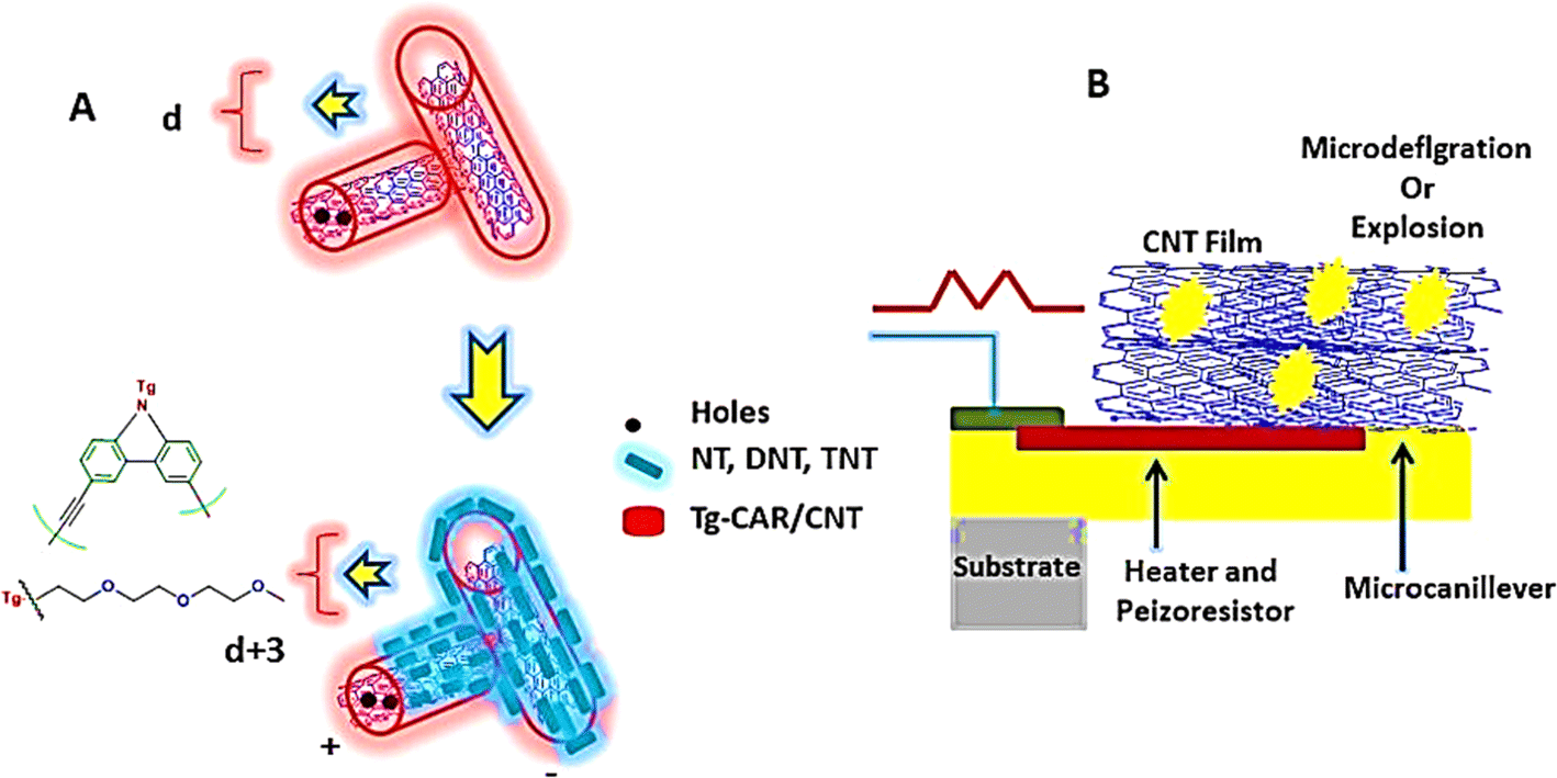 | ||
| Fig. 14 Illustrates the detection mechanisms for nitroaromatic explosives utilizing carbon nanotubes: (A) features single-walled carbon nanotubes (CNTs) that have been functionalized with Tg-Car/CNTs, and (B) showcases a piezoelectric microcantilever sensor enveloped in a CNT film. This figure delineates the application of advanced carbon nanotube technology in the sensitive and selective sensing of explosive materials.228 | ||
The arsenal for explosive trace detection (ETD) is broadened with the inclusion of carbon dots, a form of nano-carbon distinguished by its fluorescent properties and chemical stability.252 M. Wang et al.253 have crafted a magnetic carbon dot-based molecularly imprinted polymer (MIP) composite engineered for detecting trinitrophenol (TNP) with a detection limit of 0.5 nM. In another development, B. Ju et al.254 utilized a straightforward solvothermal method to create carbon dots from o-phenylenediamine and chloroform. A colorimetric sensor employing these carbon dots demonstrated a detection limit of 2 μM. These carbon dots were fixed onto ordinary filter paper, illustrating a real-world application proving the viability of using this sensor technology in various environments.
Filanovsky et al.255 investigated the use of modified carbon electrodes, augmented with mesoporous titanium dioxide as a base, with ruthenium, platinum, or gold nanoparticles deposited on top for TNT detection. The use of TiO2–PtNP and TiO2–AuNP electrodes brought significant benefits, such as the clear separation of TNT from oxygen reduction signals, increased sensitivity, and a stable linear correlation between peak currents and TNT levels. In another study, M. Riskin et al.256 utilized gold nanoparticles (AuNPs) to enhance the sensitivity of electrochemical detection techniques for TNT. They developed a functionalized electrode that could detect TNT at parts per trillion levels by attaching AuNPs to an Au electrode and interconnecting them with oligoaniline chains. This configuration, optimized by adjusting the donor–acceptor interactions between TNT and the donor-linked AuNPs, also included molecular recognition sites within the oligoaniline-linked AuNPs, further boosting sensitivity to detect TNT concentrations as low as 200 picomolar (pM).
Y. Jiang et al.257 developed a colorimetric technique for detecting TNT at the picomolar level, utilizing gold nanoparticles in a streamlined approach. This method hinges on the color shift of AuNPs, prompted by the donor–acceptor interactions between TNT and cysteamine. Cysteamine serves a dual role: it acts as a primary amine and stabilizes the AuNPs. When TNT is introduced into the solution, the cysteamine-stabilized AuNPs cluster together, leading to a color transition from red to violet blue, as illustrated in Fig. 15. The Jiang257 group noted a discernible color change visible to the naked eye when adding 114 pg L−1 of TNT to the mixture.
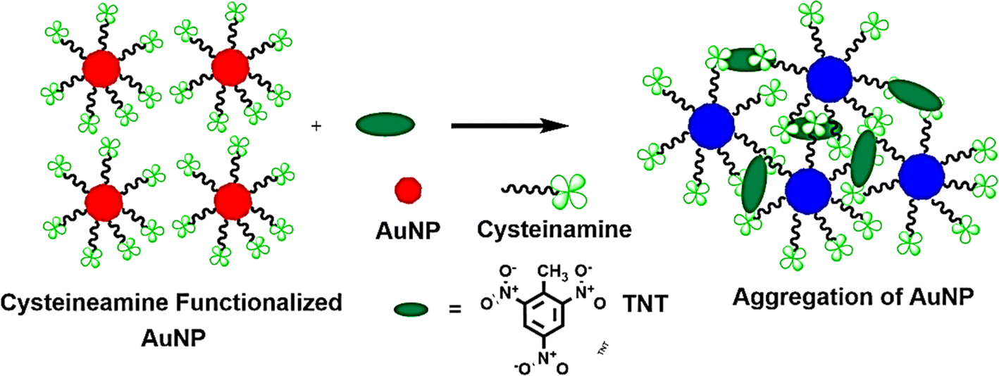 | ||
| Fig. 15 Presents a schematic depiction of the direct colorimetric method for detecting TNT, elucidating the electronic interactions between cysteamine and TNT. This illustration captures the fundamental principles underpinning the colorimetric response triggered by these interactions.228 | ||
Surface-enhanced Raman spectroscopy (SERS) is recognized as an exceptionally sensitive method for detecting molecular entities, including trace amounts of explosives.258 S. S. R. Dasary et al.259 showed that when modified with cysteine, gold nanoparticles serve as efficient SERS probes for detecting TNT in water at concentrations as low as 2 picomolar (pM). This detection capability is attributed to forming the Meisenheimer complex between TNT and cysteine on the gold nanoparticles, creating “hot spots” that significantly boost the Raman signal. Enhancing this technique, L. Yang et al.260 pushed the boundaries of SERS-based TNT detection by employing silver nanoparticles functionalized with p-aminothiophenol (PATP) and encapsulated on silver molybdate nanowires. The PATP molecules on the silver nanoparticles undergo a catalytic coupling reaction to form dimercaptoazobenzene (DMAB), establishing imprint molecule sites that act as SERS “hot spots” and significantly intensify the Raman signal. This approach's detection limit for TNT was pinpointed at around 10 femtomolar (fM).
7. Applications of machine learning in the nanosensors field
As mentioned earlier, nanomaterial-based sensor platforms are becoming up-and-coming tools for versatile and ultra-sensitive detection.261–263 Their appeal lies in finely tuning optical, electrical, and electrochemical properties, enabling fast readouts, portability, and ease of use.264,265 However, several challenges must be addressed to translate nanosensor technologies into practical applications.1,266 These challenges include detecting analyte concentrations at ultralow levels (down to parts per billion or nanomolar levels), coping with complex sample matrices containing numerous interfering species, addressing issues related to differentiating isomers and structural analogs, and managing intricate, multidimensional datasets.267,268 Advanced artificial intelligence techniques, including machine learning (ML), could help to boost the performance of this kind of sensors for medical applications,269 nanotoxicology,270 neural prosthesis,271 wireless technology,272 smart agriculture,273 environmental monitoring,274 and advanced medical manufacturing technologies.275ML is a pivotal category within the realm of informatics, offering methodologies that enable machines to learn from data autonomously. This capability empowers machines to discern patterns and correlations within datasets, granting them valuable technical utility.276–280 It has rapidly evolved from being a concept in science fiction to an integral part of everyday life. It plays a fundamental role in various sectors, including self-driving cars,281 the energy sector,282 chemical science,283 web chats,284 spam filters,285 material science,286 and face recognition.287 ML is executed through artificial neural networks (ANNs) comprising interconnected computing elements known as artificial neurons. This terminology parallels the hypothesized functioning of biological neurons in living organisms. ANNs are primarily tasked with analyzing extensive sets of interrelated data inputs and determining an optimal set of weights that describe the correlations within the dataset. This capability proves especially beneficial when dealing with large datasets where discerning patterns or correlations may be challenging or unclear. The efficacy of an ANN model improves with the dataset's size and the refinement of the neural network's structure. Neurons within ANNs are organized into “layers” that connect the model's input and output. Each layer contains varying numbers of neurons, depending on the input and output characteristics. In the initial layer, each neuron receives input and transmits it to subsequent layer neurons by applying a weight. Identifying and optimizing these weights constitute the core of the computational process, often termed the “learning” process within ANNs. Commonly utilized ML models include the multilayer perceptron (MLP), support vector machine (SVM), decision tree (DT), relevance vector machine (RVM), long short-term memory (LSTM), and random forest (RF).
The integration of advanced nanosensors and machine learning has been shown to have promising applications in different industries and engineering systems, including human–machine interactions, the food industry,288 water quality monitoring,289 agriculture,290 healthcare, manufacturing processes, environmental monitoring, and smart homes. For instance, the integration between ML and nanosensors has been exploited in disease X detection.291 In this application, nanosensors are used to identify signals in biological samples from infected people triggered by one or more biomarkers. Using artificial intelligence-based cloud computing approaches, this integration helps handle huge data with high scalability, flexibility, and cost-effectiveness. The need for cloud computing is growing along with the development of nanosensors since these technologies can handle the processing, storing, and analysis of large amounts of data produced by sensors. As a result, cloud computing is vital to nanosensors, providing several benefits and influencing how they are used.292 The optical community has gradually incorporated ML and data science approaches into photonics research.293 This has resulted in several successful applications, such as optical microscopy and communication. Cloud ML in nanophotonics offers crucial computational resources for simulating complex optical structures, speeding up the creation of novel materials and devices, enabling optical simulations, design optimizations, and data processing, and facilitating the investigation of creative design approaches and technological advances.294 Furthermore, cloud computing gives wearable electronics access to more storage and computational power, accelerating the development of wearables that can process massive amounts of data in real time with high accuracy.
Additionally, cloud computing is the foundation for advanced Internet of Things (IoT) technologies, enabling computerized decision-making, intelligent home automation, and real-time data transmission.295 Cloud-based technologies provide remote management and control in robotics, allowing robots to access computational power beyond their onboard capabilities.296 Cloud computing is used by environmental monitoring systems to collect and process data from multiple sensors, resulting in more precise forecasts and prompt responses to environmental changes. Furthermore, ML-powered cloud healthcare platforms improve patient care and facilitate safe data exchange between healthcare professionals, leading to better health outcomes and easier access to medical research. In the era of quickly developing IoT technology, when massive amounts of data are regularly generated and analyzed, finding effective computing techniques has become crucial.
Medicine and healthcare have experienced rapid evolution and advancement, driven and shaped by the applications of data-driven, robust, and efficient ML technologies.297 These ML advancements improve diagnostics, treatment optimization, and overall healthcare management. Premachandran et al.298 identified metastatic signatures in the blood of lung cancer patients using a nanosensor designed for detecting lung cancer infections, as shown in Fig. 16. This nanosensor, which leveraged metastasis initiation stem cells, demonstrated the ability to detect lung cancer with just a tiny amount of blood—precisely, 5 μl. Tumorspheres generated from cancer cells, enriched with stem cells, served as the training data for the classification model. In contrast, lung fibroblast cells from a healthy cohort were used for training data. The classification model employed an ensemble of decision trees within a random forest to predict lung cancer. Test data were obtained from both cancer patients and healthy individuals. The machine learning model successfully classified the examined individuals with a specificity of 88% and a sensitivity of 100%. The developed machine learning algorithm effectively predicted the likelihood of lung cancer metastases. Achieving a sensitivity and specificity of 100%, this model enabled the prediction of metastasis, making it possible to diagnose both primary and metastatic lung cancer. The established model removes the necessity for time-consuming isolation procedures and presents a method for detecting biomarkers without labels. The nanosensors employed in this investigation provide significant improvements, enabling the precise identification of metastasis in the bloodstream with sensitivity at the level of individual cells. Yaari et al.299 investigated a perception-driven sensing system to detect various biomarkers in human biofluids. Using photoluminescence, they employed a sensor array based on DNA-linked single-walled carbon nanotubes. Using an artificial molecular perception system, a new approach was suggested for identifying multiple biomarkers in biofluids for disease diagnosis. Optical responses were harnessed to train machine learning models, including SVM, MLP, and RF, to identify gynecologic cancer biomarkers in laboratory-generated samples and patient fluids. Qureshi et al.300 emphasized the advantages of incorporating ML into biosensor design at an individual patient level, offering benefits for disease prediction and data interpretation considering the detection of SARS-CoV-2 disease as a case study. They employed a Bayesian optimizer to reverse the design of biosensors, employing pre-defined NMs, which enabled the creation of a programmable biosensor. This approach facilitates the attainment of desired chemical and optical characteristics with improved sensitivity. Kumar et al.301 introduced a highly sensitive gold/Ti3C2Tx-coated-based sensor designed to diagnose cancer patients. A hybrid gold/Ti3C2Tx layer was applied circularly to induce surface plasmon resonance over the photonic crystal fiber. This coating method is based on the coupled mode theory. Simulations and numerical analyses were performed utilizing the finite element method. The resonance wavelength shift between cancerous and normal cell samples was measured to determine wavelength resolution and sensitivity.
 | ||
| Fig. 16 Lung cancer diagnosis using metastasis initiation stem cells nanosensor and ML.298 | ||
Furthermore, they analyzed parametric variation optimization using an ML technique, achieving a good optimization accuracy with a little error of 0.01525. Sensitivity analysis with an MLP model exhibited a 2% error. The developed sensor, combined with the application of ML, indicates that this sensor has the potential to function as a rapid, efficient, and low-cost device for detecting infected cases.
In the field of materials science, discovering recipes that produce NMs with specific optical properties is a labor-intensive and time-consuming process. ML approaches could help discover novel NMs with varied compositions and rediscover NPs with diverse properties that rely on size and form. NPs must be created with carefully regulated properties for photovoltaics, chemical sensing, thermoelectrics, catalysis, medical diagnostics, or pharmaceutics.302 R. Mohammadzadeh kakhki and M. Mohammadpoor303 employed ML algorithms to optimize the synthesis process of carbon dots with enhanced properties, such as electrocatalytic activity, stability, and fluorescence. ML can effectively be used to screen carbon dot precursors and predict their properties. Mahata et al.304 optimized the synthesis process of SnO2 nanopetals used in nanosensor fabrication. Nayak et al.305 fabricated LiFe5O8-based nanosensors using a single-step hydrothermal technique. The sensor's selectivity issue was tackled using simpler ML algorithms, including K-nearest neighbor, RF, DT, and SVM. These algorithms are employed to enhance the sensor's ability to distinguish and selectively respond to specific target analytes. DT was declared the optimal classification model, emerging as the most effective with an impressive accuracy of 98%. This indicates the high performance and reliability of the developed ML model in accurately classifying and addressing the objectives of the task at hand.
Despite their high dimensionality, analytical chemistry has successfully applied ML tools to extract quantitative and qualitative data from complex measurements.306 The use of ML in analytical chemistry has proven valuable for enhancing the analysis and interpretation of intricate chemical data. Ge et al.307 developed a robust wireless intelligent approach for detecting mycophenolic acid in silage based on electrochemical nanosensor characteristics. The nanosensor electrode comprised zinc-cobalt metal–organic frameworks/titanium carbide and MXene/iron oxide-graphene oxide. The developed MLP model comprised one input, one output, and five neurons in the hidden layer. The developed ML model showed good computational fitting between pH as the input and mycophenolic acid as the output. Unfortunately, monitoring mycotoxins on a real-time basis had not been accomplished. Zhu et al.308 established an intelligent-based nanosensing platform by utilizing MLP, SVM, and RVM to ultra-trace carbendazim residues in rice and tea. The nanosensing materials were composed of Ag–Au nano shuttles/graphene-like titanium carbide. They were used for both surface-enhanced Raman scattering and electrochemical detection. RVM model outperformed MLP and SVM for intelligent analysis of carbendazim.
Electronic sensing technology is already extensively employed to assess the quality of various products, contributing to enhancing product quality across diverse industries. These sensors are crucial in monitoring and controlling various parameters, ensuring products meet specified standards and quality criteria. The applications of electronic sensing sensors span multiple sectors, including manufacturing, agriculture, food production, and environmental monitoring, among others. ML methods have found extensive applications in solving real-world production problems, addressing challenges that are often difficult to tackle using traditional methods in various engineering fields. These methods have proven valuable in optimizing processes, predicting outcomes, identifying patterns, and enhancing decision-making across different engineering aspects, contributing to increased efficiency and improved solutions in complex scenarios. Bian et al.309 employed ML techniques to develop a calibration method for field-effect transistor devices based on carbon nanotubes, as shown in Fig. 17. The procedure commenced with the implementation of linear regression, which was then followed by the utilization of regression splines to accommodate the non-linearities present in the data. Regression trees were introduced to improve the model performance, and further enhancements were made by incorporating an RF model to reduce model variance. The resulting performance, assessed by R2, is estimated at 0.8260 using out-of-bag error. This method successfully prevents saturation and broadens the dynamic range of nanosensors by as much as 12 orders of magnitude in analyte concentrations. Additional exploration into the sensing mechanism involves examining the significance of features in each model tested. Employing machine learning methods to pinpoint features in the transistor signal that closely correlate with concentration shifts provides a valuable understanding of the carbon nanotube sensing mechanism. This contributes to the informed design of forthcoming nanosensors. Lin et al.310 introduced an ultra-sensitive and highly accurate method for identifying various pollutants, utilizing a cascade-enhanced nanosensor in conjunction with ML algorithms, as shown in Fig. 18. The surface-enhanced Raman scattering (SERS) substrate employed exhibits the capability to generate cascading electromagnetic energy, achieving a remarkable enhancement factor of up to 8.35 × 10⁹. This extraordinary enhancement is attributed to the synergistic combination of a micro-level polystyrene sphere porous array and nano-level Au–Ag clusters within the substrate. Leveraging its high cleanliness and ultra-sensitivity, the nanosensor successfully distinguished multiple hazardous pollutants with similar geometry and Raman peaks at ultra-low concentrations, supported by principal component analysis. The integration of this efficient and clean SERS substrate with artificial intelligence holds the potential to propel the application of SERS technology for the accurate identification of trace contaminants. The developed SERS substrate demonstrates significant potential and promising prospects in diverse fields, including food analysis, environmental monitoring, pharmaceuticals, and electrochemistry. An SVM model was constructed to discriminate between the Raman spectra of SERS fabricated through magnetron sputtering technology, achieving a correct classification percentage of 83%.311 Hu et al.312 demonstrated the efficacy of RF as a machine-learning model for predicting signals of SERS in a trans-1,2-bis(4-pyridyl)ethylene molecule situated on an Au substrate. The ML protocol accurately forecasts vibrational frequencies and Raman intensities using geometric descriptors derived from quantum chemistry simulations involving thousands of ab initio molecular dynamics conformations. The resulting spectra closely align with density functional theory calculations and experimental observations. Moreover, the protocol's robust transferability is evident in the predicted SERS responses of the molecule on diverse surfaces and under external influences such as electric fields and solvent environments. Wu et al.313 introduced an innovative method for developing high-performance SERS sensors by employing self-assembled Au NPs on glass capillaries. The surface self-assembly technique guarantees consistent and reproducible quality of SERS substrates, tackling the typical problem of poor reproducibility in traditional methods. The 30 nm Au nanoparticles chosen showcase excellent plasmonic properties and biocompatibility, rendering them well-suited for SERS applications. The analyzed substrate exhibits significant uniformity and repeatability, with a relative standard deviation of 12.1%. Machine learning methods like normalization, baseline correction, and smoothing were utilized in data processing to enhance the accuracy and reliability of the SERS analysis. Three separate clusters of spectral characteristics were distinguished using the K-means clustering algorithm. Furthermore, Principal Component Analysis (PCA) was employed to visually represent and interpret the clustering outcomes in a two-dimensional space, capturing roughly 86.74% of the data's variance. Lussier et al.314 reported the creation and utilization of ML algorithms combined with a SERS nanoprobe. This approach allowed for the simultaneous measurement of gradients for at least eight metabolites in vitro near various cell lines. The findings showed a significant increase in the secretion or consumption of lactate, glucose, ATP, glutamine, and urea within a 20 μm proximity to the cell surface compared to the bulk. The results also indicated that cancerous cells (HeLa) exhibited a higher glycolytic rate than fibroblasts (REF52), consistent with the expected phenotype. Both endothelial cells (HUVEC) and HeLa cells showed a notable increase in extracellular ATP compared to the control, highlighting the significance of extracellular ATP within the cancer's local environment. The ML-driven SERS optophysiology approach broadly applies to metabolites involved in cellular processes, establishing a versatile platform for studying cell biology. This technique holds potential applicability for addressing various significant challenges, including monitoring the effects of drug treatments on cells, viruses, and bacteria. Moreover, it may have relevance for in vivo experiments. Revignas and Amendola315 devised a straightforward attempt for detecting glutathione (GSH) utilizing surface Au NPs. The variation in the electric double layer of the Au NPs, influenced by increasing GSH concentration, leads to particle aggregation, resulting in a noticeable color change that can be measured. This phenomenon, commonly leveraged for optical sensing, has been incorporated into an undergraduate course to acquaint students with concepts related to NPs, colloids, colloidal stability, and sensor attributes such as selectivity, sensitivity, and detection range. They employed ML models to quantitatively correlate the corresponding absorption characteristics of Au-based sensors to analyte concentration.
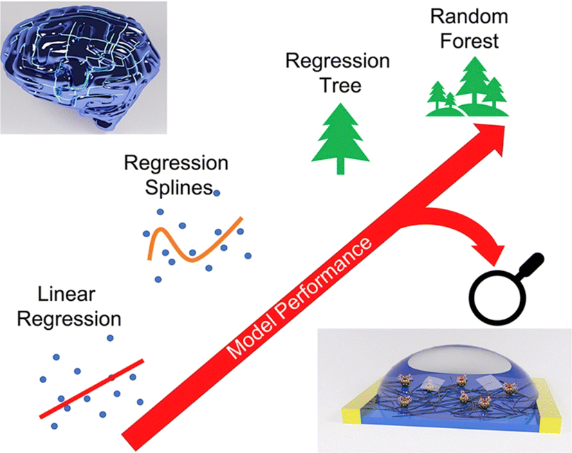 | ||
| Fig. 17 Electronic nanosensors calibration using linear regression, regression splines regression tree, and random forest.309 | ||
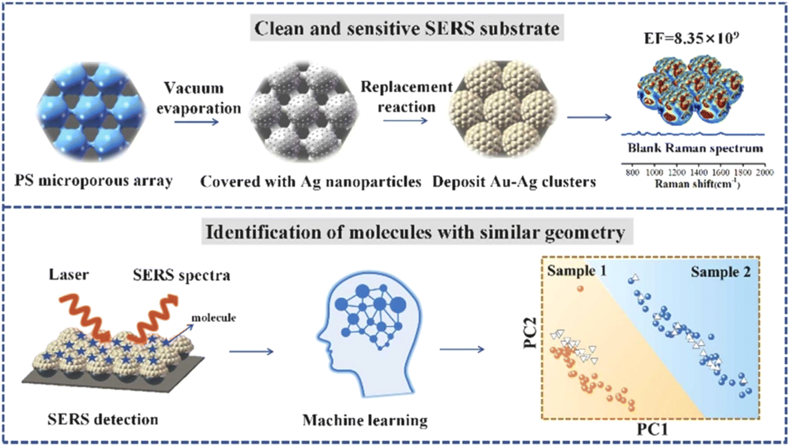 | ||
| Fig. 18 Detection of pollutants based on SERS sensors assisted by ML algorithms.310 | ||
Analyzing the toxicity of NPs is crucial for assessing the safety of NMs and understanding their potential impact on biological systems.316 However, traditional experimental methods for evaluating nanoparticle toxicity can be expensive and time-consuming. As an alternative approach, machine learning provides a solution for predicting cellular responses to NPs. This method leverages computational models and algorithms to analyze data and make predictions, offering a more efficient and cost-effective way to assess nanoparticle toxicity than traditional experimental methods. Ku et al.317 employed electrochemical sensors, semiconductor metal oxide sensors, and photoionization detection sensors to discern chemical hazards through the utilization of ML. This integrated sensor system, leveraging various sensing technologies, enables the identification and discrimination of different chemical substances. ML algorithms enhance the ability to analyze and interpret the sensor data effectively. Sensing data inputs were utilized in either image or numerical data, and the classification of chemical hazards with high accuracy was achieved in both cases. This flexibility in data input formats demonstrates the versatility and effectiveness of the approach, showcasing the ability to leverage diverse types of sensor data for accurate chemical hazard classification. The efficacy of ML-based gas discrimination is demonstrated by its ability to leverage even small amounts of gas sensing or purging data, typically input for around 30 seconds. This highlights the efficiency of the approach in extracting valuable information from relatively brief sensing periods, making it practical for real-time applications and enhancing the feasibility of gas discrimination tasks. Wang et al.318 developed a fluorescence sensor enhanced by ML for sulfide determination. This sensor incorporated a nanometal-organic framework (UiO-66-NH2) and protoporphyrin IX (Ppix). The blue fluorescence at 431 nm, originating from the UiO-66-NH2 moiety upon 365 nm excitation, served as an internal calibration reference signal. Simultaneously, the red fluorescence at 629 nm from the Ppix moiety served as the analytical signal, with intensity correlated to the amount of sulfides. The fluorescence color of the sensor gradually transitioned from blue to red with the sequential addition of copper and sulfide ions. This variation led to color characteristics based on RGB values corresponding to sulfide concentrations, enabling advanced data processing techniques through ML algorithms. They further developed an online data analysis model based on fluorescence image fingerprint extraction and ML algorithms to improve the precision and accuracy of sulfide determination. The model, employing Linear Discriminant Analysis (LDA) and undergoing rigorous cross-validation, demonstrated a significant positive relationship between red feature values and sulfide concentrations. This comprehensive approach presents a powerful tool for environmental monitoring and pollution detection. Long et al.319 developed an ML-assisted dual-channel visual sensor array to identify the origin of Lilium bulbs (BH). They utilized quantum dots and nanogold clusters as components in the sensor arrays. The presence of amino acids in Lilium bulbs induced an aggregation-induced fluorescence enhancement effect of nanogold clusters through hydrogen bonding. The reported outcomes revealed that the developed dual-channel visual sensor and the utilized ML model exhibited a high accuracy of 94.4% for identifying lilium bulbs from eight different origins. This achievement underscores the system's capability for rapid and accurate traceability of Lilium bulbs from various geographical locations. The success of this approach holds promising application prospects, particularly in the context of food traceability.
This review is anticipated to provide analytical chemists and researchers with a deeper understanding of the recent advancements in ML-assisted nanosensor arrays, particularly in various engineering applications. Considering the substantial advancements achieved by nanosensors in engineering fields, it is expected that machine learning-assisted nanosensor arrays based on functional NMs will find practical applications. However, integrating ML and nanosensors in real-life applications faces a significant obstacle—ultimately, a lack of trust in the model predictivity, primarily stemming from poor model interpretability. As datasets increase in dimensionality, researchers must resort to more intricate ML algorithms to enhance predictive performance. Nevertheless, these ML systems are frequently characterized as ‘black boxes' and face unclear and ambiguous decision-making issues, impacting their reliability.
Consequently, there has been a noticeable shift in emphasis towards ‘explainable machine learning’ aimed at enhancing model interpretability. This involves enabling algorithms to trace and elucidate their decision-making processes in a way researchers can understand. For instance, sophisticated techniques should be employed to assess the relative significance of input features in a constructed model. This information can offer better guidance for selecting scientifically relevant input features when interpreted alongside domain knowledge. Recently, advanced model frameworks have been developed to incorporate additional constraints, allowing the generation of various interpretable explanations that specifically include selected essential features. This becomes particularly valuable for generating more specific interpretations by employing different input feature subspaces. These subspaces can elucidate explanations for either a single or smaller sample subset. Incorporating explainable ML algorithms is crucial for instilling greater confidence in ML models' robustness and scientific validity. It facilitates their widespread integration into diverse environmental, healthcare, and agri-food settings. A trend will emerge involving integrating artificial intelligence, nanotechnology, and 3D-printed technology to develop innovative portable nanosensor arrays for exact applications. This review aims to promote rational design and construction of low-cost, rapid, selective, and sensitive nanosensors for various engineering applications.
8. Conclusion
This paper provides a comprehensive review of NMs-based nanosensors as well as the advancement that has occurred recently in the development of advanced materials and nanostructures, with their extraordinary combinations of thermal, electrical, mechanical, and optical properties, which has dramatically expanded the limits in the field of nanosensors. These advancements have led to a heightened interest in applications in various fields, such as environmental monitoring, the food industry, health monitoring, biomedical and industrial applications, and other safety and security controls.The use of nanosensors has the potential to revolutionize multiple sectors by providing innovative solutions for detection, monitoring, and analysis. The healthcare field stands to benefit significantly from nanosensors, as they offer new possibilities for disease diagnostics, personalized medicine, and patient monitoring. Nanosensors empower individuals to take control of their health and well-being with their ability to detect biomarkers and monitor vital signs in real time.
In addition to healthcare, nanosensors also significantly impact other industries, such as electronics, manufacturing, aerospace, and defense. By enabling precise and real-time monitoring of critical parameters, nanosensors contribute to advancements in these sectors. These miniature sensors are smaller than human hair but offer high sensitivity and specificity in detecting various biomolecules and small-molecule metabolites.
Moreover, integrating machine learning techniques with nanosensor technologies opens up new opportunities for data exploration and predictions. Clustering, classification, and regression algorithms can analyze complex multidimensional datasets with high sample variability associated with nanosensor measurements. By combining these machine learning strategies with customizable nanosensor platforms, researchers can develop multifaceted strategies that further boost the performance of nanosensors.
Looking ahead, several vital areas emerge as pivotal for future research and development in the realm of nanosensors:
1- Material innovation: continued exploration and synthesis of novel nanomaterials (NMs) with enhanced properties and functionalities will be crucial. The research will focus on discovering materials that offer excellent stability, biocompatibility, and environmental sustainability.
2- Integration with emerging technologies: the convergence of nanosensors with cutting-edge technologies such as artificial intelligence, IoT, and blockchain could revolutionize data analysis, security, and sensor networking. Future work will likely explore how these integrations can lead to more intelligent, efficient, and interconnected sensing systems.
3- Enhanced fabrication techniques: developing more efficient, cost-effective, and scalable fabrication methods remains a priority. Future research should aim to streamline manufacturing processes while maintaining the high quality and performance of nanosensors.
4- Improving sensing abilities: efforts to enhance the sensitivity and selectivity of nanosensors for specific applications, particularly in the early detection of diseases or environmental pollutants, will be crucial.
Conflicts of interest
There are no conflicts to declare.References
- M. Javaid, A. Haleem, R. P. Singh, S. Rab and R. Suman, Sensors Int, 2021, 2, 100130 CrossRef
.
- T. Yang and T. V. Duncan, Nat. Nanotechnol., 2021, 16, 251–265 CrossRef CAS PubMed
- J. Wang, ChemPhysChem, 2009, 10, 1748–1755 CrossRef CAS PubMed
- C. Zhu, G. Yang, H. Li, D. Du and Y. Lin, Anal. Chem., 2015, 87, 230–249 CrossRef CAS PubMed
- V. Nocerino, B. Miranda, C. Tramontano, G. Chianese, P. Dardano, I. Rea and L. De Stefano, Chemosensors, 2022, 10, 150 CrossRef CAS
- J. Deng, S. Zhao, Y. Liu, C. Liu and J. Sun, ACS Appl. Bio Mater., 2021, 4, 3863–3879 CrossRef CAS PubMed
- R. Abedi-Firoozjah, H. Ebdali, M. Soltani, P. Abdolahi-Fard, M. Heydari, E. Assadpour, M. Azizi-Lalabadi, F. Zhang and S. M. Jafari, Coord. Chem. Rev., 2024, 500, 215545 CrossRef CAS
- D. Han, H. Hosamo, C. Ying and R. Nie, Appl. Sci., 2023, 13, 11149 CrossRef CAS
- M. Singh, J. Truong, W. B. Reeves and J. I. Hahm, Sensors, 2017, 17, 428 CrossRef PubMed
-
S. Akgönüllü and A. Denizli, in Nanotechnology-Based Smart Remote Sensing Networks for Disaster Prevention, Elsevier, 2022, pp. 43–57 Search PubMed
- S. Manzeli, D. Ovchinnikov, D. Pasquier, O. V. Yazyev and A. Kis, Nat. Rev. Mater., 2017, 2, 17033 CrossRef CAS
-
R. Ponnusamy and C. S. Rout, in Two Dimensional Transition Metal Dichalcogenides, ed. N. S. Arul and V. D. Nithya, Springer Singapore, Singapore, 2019, pp. 293–329 Search PubMed
-
P. N. Sudha, K. Sangeetha, K. Vijayalakshmi and A. Barhoum, in Emerging Applications of Nanoparticles and Architectural Nanostructures: Current Prospects and Future Trends, Elsevier, 2018, pp. 341–384 Search PubMed
- J. Pérez-Arantegui, J. Molera, A. Larrea, T. Pradell, M. Vendrell-Saz, I. Borgia, B. G. Brunetti, F. Cariati, P. Fermo, M. Mellini, A. Sgamellotti and C. Viti, J. Am. Ceram. Soc., 2001, 84, 442–446 CrossRef
- D. J. Barber and I. C. Freestone, Archaeometry, 1990, 32, 33–45 CrossRef
- M. Reibold, N. Pätzke, A. A. Levin, W. Kochmann, I. P. Shakhverdova, P. Paufler and D. C. Meyer, Cryst. Res. Technol., 2009, 44, 1139–1146 CrossRef CAS
- D. E. Arnold, Anc. Mesoamerica, 2005, 16, 51–62 CrossRef
- F. J. Heiligtag and M. Niederberger, Mater. Today, 2013, 16, 262–271 CrossRef CAS
-
S. S. Papell, O. C. Faber, On the Influence of Nonuniform Magnetic Fields on Ferromagnetic Colloidal Sols, National Aeronautics and Space Administration 1968, https://books.google.com.eg/books?id=_culzCAS-ssC Search PubMed
- R. Kaiser and G. Miskolczy, J. Appl. Phys., 1970, 41, 1064–1072 CrossRef CAS
-
D. Sannino, in Nanotechnology: Trends and Future Applications, Springer Singapore, Singapore, 2021, pp. 15–38 Search PubMed
-
L. H. Madkour, in Advanced Structured Materials, Springer International Publishing, 2019, vol. 116, pp. 1–47 Search PubMed
-
A. B. Asha and R. Narain, in Polymer Science and Nanotechnology: Fundamentals and Applications, Elsevier, 2020, pp. 343–359 Search PubMed
- N. Joudeh and D. Linke, J. Nanobiotechnol., 2022, 20, 262 CrossRef PubMed
- F. S. Hamid, O. A. E. El-Kady, A. R. S. Essa, A. E. G. El-Nikhaily, A. Elsayed and W. Abd-Elaziem, J. Mater. Eng. Perform., 2022, 31, 5583–5592 CrossRef CAS
- H. M. Yehia, F. Nouh, O. A. El Kady, W. A. Elaziem and E. M. Elsayed, Int. J. Mach. Mach. Mater., 2022, 24, 430 Search PubMed
- Q. L. Zhu and Q. Xu, Chem, 2016, 1, 220–245 CAS
- G. Almeida, L. van der Poll, W. H. Evers, E. Szoboszlai, S. J. W. Vonk, F. T. Rabouw and A. J. Houtepen, Nano Lett., 2023, 23, 8697–8703 CrossRef CAS PubMed
- Z. Chen, J. C. Beimborn, N. Kirkwood, S. P. Russo, J. M. Weber and P. Mulvaney, J. Phys. Chem. C, 2023, 127, 8657–8669 CrossRef CAS
- B. Uprety and H. Abrahamse, Front. Chem., 2022, 10, 946574 CrossRef CAS PubMed
- M. Chen, R. Guan and S. Yang, Adv. Sci., 2019, 6, 1800941 CrossRef PubMed
- J. W. Liu, H. W. Liang and S. H. Yu, Chem. Rev., 2012, 112, 4770–4799 CrossRef CAS PubMed
- S. M. Bergin, Y. H. Chen, A. R. Rathmell, P. Charbonneau, Z. Y. Li and B. J. Wiley, Nanoscale, 2012, 4, 1996–2004 RSC
- S. Das, Int. J. Emerging Technol. Adv. Eng., 2008, 3, 774–783 Search PubMed
- A. Martinez-Hernandez, C. Velasco-Santos and V. Castano, Curr. Nanosci., 2010, 6, 12–39 CrossRef CAS
- Z. Han and A. Fina, Prog. Polym. Sci., 2011, 36, 914–944 CrossRef CAS
- A. I. Osman, W. Abd-Elaziem, M. Nasr, M. Farghali, A. K. Rashwan, A. Hamada, Y. M. Wang, M. A. Darwish, T. A. Sebaey, A. Khatab and A. H. Elsheikh, Environ. Chem. Lett., 2024 DOI:10.1007/s10311-024-01741-3
- J. Pérez-Juste, I. Pastoriza-Santos, L. M. Liz-Marzán and P. Mulvaney, Coord. Chem. Rev., 2005, 249, 1870–1901 CrossRef
- J. Zheng, X. Cheng, H. Zhang, X. Bai, R. Ai, L. Shao and J. Wang, Chem. Rev., 2021, 121, 13342–13453 CrossRef CAS PubMed
- M. E. Pearce, J. B. Melanko and A. K. Salem, Pharm. Res., 2007, 24, 2335–2352 CrossRef CAS PubMed
- A. Serrà and E. Vallés, Appl. Mater. Today, 2018, 12, 207–234 CrossRef
- V. Shabafrooz, M. Mozafari, D. Vashaee and L. Tayebi, J. Nanosci. Nanotechnol., 2014, 14, 522–534 CrossRef CAS PubMed
-
A. ElenaOprea, A. Ficai and E. Andronescu, in Materials for Biomedical Engineering: Nanobiomaterials in Tissue Engineering, Elsevier, 2019, pp. 77–95 Search PubMed
-
S. Das and W. Choi, in Graphene: Synthesis and Applications, CRC Press, 2016, vol. 3, pp. 27–63 Search PubMed
- J. Zhu, D. Yang, Z. Yin, Q. Yan and H. Zhang, Small, 2014, 10, 3480–3498 CrossRef CAS PubMed
- W. Choi, N. Choudhary, G. H. Han, J. Park, D. Akinwande and Y. H. Lee, Mater. Today, 2017, 20, 116–130 CrossRef CAS
- R. Lv, J. A. Robinson, R. E. Schaak, D. Sun, Y. Sun, T. E. Mallouk and M. Terrones, Acc. Chem. Res., 2015, 48, 56–64 CrossRef CAS PubMed
- S. Roy, X. Zhang, A. B. Puthirath, A. Meiyazhagan, S. Bhattacharyya, M. M. Rahman, G. Babu, S. Susarla, S. K. Saju, M. K. Tran, L. M. Sassi, M. A. S. R. Saadi, J. Lai, O. Sahin, S. M. Sajadi, B. Dharmarajan, D. Salpekar, N. Chakingal, A. Baburaj, X. Shuai, A. Adumbumkulath, K. A. Miller, J. M. Gayle, A. Ajnsztajn, T. Prasankumar, V. V. J. Harikrishnan, V. Ojha, H. Kannan, A. Z. Khater, Z. Zhu, S. A. Iyengar, P. A. da S. Autreto, E. F. Oliveira, G. Gao, A. G. Birdwell, M. R. Neupane, T. G. Ivanov, J. Taha-Tijerina, R. M. Yadav, S. Arepalli, R. Vajtai and P. M. Ajayan, Adv. Mater., 2021, 33(44), 2101589 CrossRef CAS PubMed
- K. Zhang, Y. Feng, F. Wang, Z. Yang and J. Wang, J. Mater. Chem. C, 2017, 5, 11992–12022 RSC
- Y. Xu, Z. Shi, X. Shi, K. Zhang and H. Zhang, Nanoscale, 2019, 11, 14491–14527 RSC
- W. Lei, G. Liu, J. Zhang and M. Liu, Chem. Soc. Rev., 2017, 46, 3492–3509 RSC
- R. D. Farahani, M. Dubé and D. Therriault, Adv. Mater., 2016, 28, 5794–5821 CrossRef CAS PubMed
- S. K. Kumar and R. Krishnamoorti, Annu. Rev. Chem. Biomol. Eng., 2010, 1, 37–58 CrossRef CAS PubMed
- D. R. Rolison, J. W. Long, J. C. Lytle, A. E. Fischer, C. P. Rhodes, T. M. Mc Evoy, M. E. Bourg and A. M. Lubers, Chem. Soc. Rev., 2009, 38, 226–252 RSC
- P. X. Gao, C. S. Lao, W. L. Hughes and Z. L. Wang, Chem. Phys. Lett., 2005, 408, 174–178 CrossRef CAS
- M. Rauber, I. Alber, S. Muöller, R. Neumann, O. Picht, C. Roth, A. Schoökel, M. E. Toimil-Molares and W. Ensinger, Nano Lett., 2011, 11, 2304–2310 CrossRef CAS PubMed
- T. Y. Poh, N. A. T. B. M. Ali, M. Mac Aogáin, M. H. Kathawala, M. I. Setyawati, K. W. Ng and S. H. Chotirmall, Part. Fibre Toxicol., 2018, 15, 46 CrossRef CAS PubMed
-
R. Jose Varghese, E. H. M. Sakho, S. Parani, S. Thomas, O. S. Oluwafemi and J. Wu, in Nanomaterials for Solar Cell Applications, Elsevier, 2019, pp. 75–95 Search PubMed
- R. K. Kankala, Curr. Pharm. Des., 2021, 28, 208–215 CrossRef PubMed
- K. Ganesan, Y. Wang, F. Gao, Q. Liu, C. Zhang, P. Li, J. Zhang and J. Chen, Pharmaceutics, 2021, 13, 1829 CrossRef CAS PubMed
-
M. Benelmekki, in Designing Hybrid Nanoparticles, Morgan
& Claypool Publishers, 2015, pp. 1-1–1-14 Search PubMed
- S. Rahmani, J. Budimir, M. Sejalon, M. Daurat, D. Aggad, E. Vivès, L. Raehm, M. Garcia, L. Lichon, M. Gary-Bobo, J.-O. Durand and C. Charnay, Molecules, 2019, 24, 332 CrossRef PubMed
- M. Tomić, M. Claros, I. Gràcia, E. Figueras, C. Cané and S. Vallejos, Sensors, 2021, 21, 4509 CrossRef PubMed
- Y. Yuan and J. Chen, Nanomaterials, 2016, 6, 36 CrossRef PubMed
- B. Salesa, M. Llorens-Gámez and Á. Serrano-Aroca, Nanomaterials, 2020, 10, 206 CrossRef CAS PubMed
- T. da Câmara Santa Clara Gomes, N. Marchal, F. Abreu Araujo, Y. Velázquez Galván, J. de la Torre Medina and L. Piraux, Nanomaterials, 2021, 11, 221 CrossRef PubMed
-
EMR/ESR/EPR Spectroscopy for Characterization of Nanomaterials, ed. A. K. Shukla, Springer India, New Delhi, 2017, vol. 62 Search PubMed
- H. Khosravi Ardakani, M. Gerami, M. Chashmpoosh, N. Omidifar and A. Gholami, Biochem. Res. Int., 2022, 2022, 2964705 CrossRef PubMed
- S.-H. Chung, H. Kim and S. W. Jeong, Carbon, 2018, 140, 24–29 CrossRef CAS
- W. Abd-Elaziem, M. Khedr, A.-E. Abd-Elaziem, M. M. A. Allah, A. A. Mousa, H. M. Yehia, W. M. Daoush and M. A. A. El-Baky, J. Inorg. Organomet. Polym. Mater., 2023, 33, 3732–3749 CrossRef CAS
- B. Jaleh, M. Nasrollahzadeh, M. Eslamipanah, A. Nasri, E. Shabanlou, N. R. Manwar, R. Zboril, P. Fornasiero and M. B. Gawande, Carbon, 2022, 198, 301–352 CrossRef CAS
- H. W. Kroto, J. R. Heath, S. C. O’Brien, R. F. Curl and R. E. Smalley, Nature, 1985, 318, 162–163 CrossRef CAS
-
J. R. Siqueira and O. N. Oliveira, in Nanostructures, Elsevier, 2017, pp. 233–249 Search PubMed
- S. Das and M. Presselt, J. Mater. Chem. C, 2019, 7, 6194–6216 RSC
- S. Iijima, Nature, 1991, 354, 56–58 CrossRef CAS
- S. Iijima and T. Ichihashi, Nature, 1993, 363, 603–605 CrossRef CAS
- K. Hata, D. N. Futaba, K. Mizuno, T. Namai, M. Yumura and S. Iijima, Science, 2004, 306, 1362–1364 CrossRef CAS PubMed
- E. I. Epelle, K. S. Desongu, W. Obande, A. A. Adeleke, P. P. Ikubanni, J. A. Okolie and B. Gunes, Int. J. Hydrogen Energy, 2022, 47, 20398–20431 CrossRef CAS
- T. Zhou and T. Zhang, Small Methods, 2021, 5(9), 2100515 CrossRef CAS PubMed
- Y.-L. Li, I. A. Kinloch and A. H. Windle, Science, 2004, 304, 276–278 CrossRef CAS PubMed
- J. Chrzanowska, J. Hoffman, A. Małolepszy, M. Mazurkiewicz, T. A. Kowalewski, Z. Szymanski and L. Stobinski, Phys. Status Solidi, 2015, 252, 1860–1867 CrossRef CAS
- M. Keidar, A. Shashurin, J. Li, O. Volotskova, M. Kundrapu and T. Sen Zhuang, J. Phys. D Appl. Phys., 2011, 44, 174006 CrossRef
- V. Dhinakaran, M. Lavanya, K. Vigneswari, M. Ravichandran and M. D. Vijayakumar, Mater. Today: Proc., 2020, 27, 824–828 CAS
- S. Velusamy, A. Roy, S. Sundaram and T. Kumar Mallick, Chem. Rec., 2021, 21, 1570–1610 CrossRef CAS PubMed
- T. Iqbal, S. Fatima, T. Bibi and M. Zafar, Opt. Quantum Electron., 2021, 53, 228 CrossRef CAS
- K. S. Novoselov, A. K. Geim, S. V. Morozov, D. Jiang, Y. Zhang, S. V. Dubonos, I. V. Grigorieva and A. A. Firsov, Science, 2004, 306, 666–669 CrossRef CAS PubMed
- A. K. Geim and K. S. Novoselov, Nat. Mater., 2007, 6, 183–191 CrossRef CAS PubMed
- X. Li, X. Wang, L. Zhang, S. Lee and H. Dai, Science, 2008, 319, 1229–1232 CrossRef CAS PubMed
- X. Li, G. Zhang, X. Bai, X. Sun, X. Wang, E. Wang and H. Dai, Nat. Nanotechnol., 2008, 3, 538–542 CrossRef CAS PubMed
- P. Blake, P. D. Brimicombe, R. R. Nair, T. J. Booth, D. Jiang, F. Schedin, L. A. Ponomarenko, S. V. Morozov, H. F. Gleeson, E. W. Hill, A. K. Geim and K. S. Novoselov, Nano Lett., 2008, 8, 1704–1708 CrossRef PubMed
- Y. Hernandez, V. Nicolosi, M. Lotya, F. M. Blighe, Z. Sun, S. De, I. T. McGovern, B. Holland, M. Byrne, Y. K. Gun’Ko, J. J. Boland, P. Niraj, G. Duesberg, S. Krishnamurthy, R. Goodhue, J. Hutchison, V. Scardaci, A. C. Ferrari and J. N. Coleman, Nat. Nanotechnol., 2008, 3, 563–568 CrossRef CAS PubMed
- J. Lu, J. Yang, J. Wang, A. Lim, S. Wang and K. P. Loh, ACS Nano, 2009, 3, 2367–2375 CrossRef CAS PubMed
- N. Liu, F. Luo, H. Wu, Y. Liu, C. Zhang and J. Chen, Adv. Funct. Mater., 2008, 18, 1518–1525 CrossRef CAS
- M. Saeed, Y. Alshammari, S. A. Majeed and E. Al-Nasrallah, Molecules, 2020, 25, 3856 CrossRef CAS PubMed
- P. Sutter, C. V. Ciobanu and E. Sutter, Small, 2012, 8, 2250–2257 CrossRef CAS PubMed
- M. Huang and R. S. Ruoff, Acc. Chem. Res., 2020, 53, 800–811 CrossRef CAS PubMed
- V. Y. Aristov, G. Urbanik, K. Kummer, D. V. Vyalikh, O. V. Molodtsova, A. B. Preobrajenski, A. A. Zakharov, C. Hess, T. Hänke, B. Büchner, I. Vobornik, J. Fujii, G. Panaccione, Y. A. Ossipyan and M. Knupfer, Nano Lett., 2010, 10, 992–995 CrossRef CAS PubMed
- N. Mishra, J. Boeckl, N. Motta and F. Iacopi, Phys. Status Solidi, 2016, 213, 2277–2289 CrossRef CAS
- J. Gaidukevic, R. Aukstakojyte, T. Navickas, R. Pauliukaite and J. Barkauskas, Appl. Surf. Sci., 2021, 567, 150883 CrossRef CAS
- S. Shamaila, A. K. L. Sajjad and A. Iqbal, Chem. Eng. J., 2016, 294, 458–477 CrossRef CAS
- Y. V. Ioni, S. I. Chentsov, I. V. Sapkov, E. G. Rustamova and S. P. Gubin, Russ. J. Inorg. Chem., 2022, 67, 1711–1717 CrossRef CAS
- S. K. Krishnan, E. Singh, P. Singh, M. Meyyappan and H. S. Nalwa, RSC Adv., 2019, 9, 8778–8881 RSC
- A. T. Dideikin and A. Y. Vul, Front. Phys., 2019, 6 DOI:10.3389/fphy.2018.00149
- J. G. S. Moo, B. Khezri, R. D. Webster and M. Pumera, ChemPhysChem, 2014, 15, 2922–2929 CrossRef CAS PubMed
- F. A. M. Al-Zahrani, B. M. Al-Shehri, R. M. El-Shishtawy, N. S. Awwad, K. A. Khan, M. A. Sayed and S. M. Siddeeg, Materials, 2022, 15, 8136 CrossRef CAS PubMed
- P. P. Brisebois and M. Siaj, J. Mater. Chem. C, 2020, 8, 1517–1547 RSC
- O. A. Williams, M. Nesladek, M. Daenen, S. Michaelson, A. Hoffman, E. Osawa, K. Haenen and R. B. Jackman, Diamond Relat. Mater., 2008, 17, 1080–1088 CrossRef CAS
- V. N. Mochalin, O. Shenderova, D. Ho and Y. Gogotsi, Nat. Nanotechnol., 2012, 7, 11–23 CrossRef CAS PubMed
- J.-X. Qin, X.-G. Yang, C.-F. Lv, Y.-Z. Li, K.-K. Liu, J.-H. Zang, X. Yang, L. Dong and C.-X. Shan, Mater. Des., 2021, 210, 110091 CrossRef CAS
- V. Pichot, M. Comet, E. Fousson, C. Baras, A. Senger, F. Le Normand and D. Spitzer, Diamond Relat. Mater., 2008, 17, 13–22 CrossRef CAS
- M. Frenklach, W. Howard, D. Huang, J. Yuan, K. E. Spear and R. Koba, Appl. Phys. Lett., 1991, 59, 546–548 CrossRef CAS
- T. L. Daulton, M. A. Kirk, R. S. Lewis and L. E. Rehn, Nucl. Instrum. Methods Phys. Res., Sect. B, 2001, 175–177, 12–20 CrossRef CAS
- J.-P. Boudou, P. A. Curmi, F. Jelezko, J. Wrachtrup, P. Aubert, M. Sennour, G. Balasubramanian, R. Reuter, A. Thorel and E. Gaffet, Nanotechnology, 2009, 20, 235602 CrossRef PubMed
- G.-W. Yang, J.-B. Wang and Q.-X. Liu, J. Phys.: Condens.Matter, 1998, 10, 7923–7927 CrossRef CAS
- Y. Xia, P. Yang, Y. Sun, Y. Wu, B. Mayers, B. Gates, Y. Yin, F. Kim and H. Yan, Adv. Mater., 2003, 15, 353–389 CrossRef CAS
- G. Zou, D. Zhang, C. Dong, H. Li, K. Xiong, L. Fei and Y. Qian, Carbon, 2006, 44, 828–832 CrossRef CAS
- T. D. Nguyen and J. S. Lee, Appl. Sci., 2022, 12, 6048 CrossRef CAS
- R. Cui, D. Xu, X. Xie, Y. Yi, Y. Quan, M. Zhou, J. Gong, Z. Han and G. Zhang, Food Chem., 2017, 221, 457–463 CrossRef CAS PubMed
- J. S. Lee, O. S. Kwon, S. J. Park, E. Y. Park, S. A. You, H. Yoon and J. Jang, ACS Nano, 2011, 5, 7992–8001 CrossRef CAS PubMed
- M. Shooshtari, L. N. Sacco, J. Van Ginkel, S. Vollebregt and A. Salehi, Materials, 2022, 15, 1383 CrossRef CAS PubMed
- A. Walcarius, Sensors, 2017, 17, 1863 CrossRef PubMed
- C. Fu, D. Yi, C. Deng, X. Wang, W. Zhang, Y. Tang, F. Caruso and Y. Wang, Chem. Mater., 2017, 29, 5286–5293 CrossRef CAS
- R. Blume, D. Rosenthal, J. Tessonnier, H. Li, A. Knop-Gericke and R. Schlögl, ChemCatChem, 2015, 7, 2871–2881 CrossRef CAS
- A. Kovtun, D. Jones, S. Dell'Elce, E. Treossi, A. Liscio and V. Palermo, Carbon, 2019, 143, 268–275 CrossRef CAS
- V. Panchal, Y. Yang, G. Cheng, J. Hu, M. Kruskopf, C.-I. Liu, A. F. Rigosi, C. Melios, A. R. Hight Walker, D. B. Newell, O. Kazakova and R. E. Elmquist, Commun. Phys., 2018, 1, 83 CrossRef PubMed
-
M. Kakihana and M. Osada, in Carbon Alloys, Elsevier, 2003, pp. 285–298 Search PubMed
-
M. Szybowicz, A. B. Nowicka and A. Dychalska, in Characterization of Nanomaterials, Elsevier, 2018, pp. 1–36 Search PubMed
-
J. Mast, E. Verleysen, V.-D. Hodoroaba and R. Kaegi, in Characterization of Nanoparticles, Elsevier, 2020, pp. 29–48 Search PubMed
-
K. Akhtar, S. A. Khan, S. B. Khan and A. M. Asiri, in Handbook of Materials Characterization, Springer International Publishing, Cham, 2018, pp. 113–145 Search PubMed
- K. Cheng, S. Wallaert, H. Ardebili and A. Karim, Carbon, 2022, 194, 81–103 CrossRef CAS
- H. Malekzad, P. Sahandi Zangabad, H. Mirshekari, M. Karimi and M. R. Hamblin, Nanotechnol. Rev., 2017, 6, 301–329 CAS
- B. Wu, Y. Kuang, X. Zhang and J. Chen, Nano Today, 2011, 6, 75–90 CrossRef CAS
- A. Biswas, I. S. Bayer, A. S. Biris, T. Wang, E. Dervishi and F. Faupel, Adv. Colloid Interface Sci., 2012, 170, 2–27 CrossRef CAS PubMed
- M. Azharuddin, G. H. Zhu, D. Das, E. Ozgur, L. Uzun, A. P. F. Turner and H. K. Patra, Chem. Commun., 2019, 55, 6964–6996 RSC
- C. Daruich De Souza, B. Ribeiro Nogueira and M. E. C. M. Rostelato, J. Alloys Compd., 2019, 798, 714–740 CrossRef CAS
- A. Oyelere, Nanotechnol., Sci. Appl., 2008, 1, 45–66 CrossRef PubMed
- A. M. El Shafey, Green Process. Synth., 2020, 9, 304–339 Search PubMed
-
M. Ravichandran, P. Kanniah and M. Kasi, in Silver Nanomaterials for Agri-Food Applications, Elsevier, 2021, pp. 103–123 Search PubMed
- M. Rafique, I. Sadaf, M. S. Rafique and M. B. Tahir, Artif. Cells, Nanomed., Biotechnol., 2017, 45, 1272–1291 CrossRef CAS PubMed
- M. A. R. Khan, M. S. Al Mamun and M. H. Ara, Microchem. J., 2021, 171, 106840 CrossRef CAS
- K. Tahir, S. Nazir, A. Ahmad, B. Li, A. U. Khan, Z. U. H. Khan, F. U. Khan, Q. U. Khan, A. Khan and A. U. Rahman, J. Photochem. Photobiol., B, 2017, 166, 246–251 CrossRef CAS PubMed
- X. Zhou, X. Dai, J. Li, Y. Long, W. Li and Y. Tu, Mater. Sci. Eng. C, 2015, 49, 579–587 CrossRef CAS PubMed
-
D. Kishore Kumar, K. Raghava Reddy, V. Sadhu, N. P. Shetti, C. Venkata Reddy, R. S. Chouhan and S. Naveen, in Nanomaterials in Diagnostic Tools and Devices, Elsevier, 2020, pp. 113–129 Search PubMed
- L. Silipigni, F. Barreca, E. Fazio, F. Neri, T. Spanò, S. Piazza, C. Sunseri and R. Inguanta, J. Phys. Chem. C, 2014, 118, 22299–22308 CrossRef CAS
- A. J. Haider, R. H. AL-Anbari, G. R. Kadhim and C. T. Salame, Energy Procedia, 2017, 119, 332–345 CrossRef CAS
- P. Hassanpour, Y. Panahi, A. Ebrahimi-Kalan, A. Akbarzadeh, S. Davaran, A. N. Nasibova, R. Khalilov and T. Kavetskyy, Micro Nano Lett., 2018, 13, 1227–1231 CrossRef CAS
- R. Wahab and M. Alam, Sens. Actuators, A, 2022, 347, 113967 CrossRef CAS
- S. B. Khan, M. Faisal, M. M. Rahman and A. Jamal, Sci. Total Environ., 2011, 409, 2987–2992 CrossRef CAS PubMed
- B. B. Kamble, M. Naikwade, K. M. Garadkar, R. B. Mane, K. K. K. Sharma, B. D. Ajalkar and S. N. Tayade, J. Mater. Sci.: Mater. Electron., 2019, 30, 13984–13993 CrossRef CAS
- M. Zheng, W. Li, M. Xu, N. Xu, P. Chen, M. Han and B. Xie, Nanoscale, 2014, 6, 3930–3933 RSC
- M. Bushell, S. Beauchemin, F. Kunc, D. Gardner, J. Ovens, F. Toll, D. Kennedy, K. Nguyen, D. Vladisavljevic, P. E. Rasmussen and L. J. Johnston, Nanomaterials, 2020, 10, 1812 CrossRef CAS PubMed
- Y. He, C. Fan and S.-T. Lee, Nano Today, 2010, 5, 282–295 CrossRef CAS
- X. Ji, H. Wang, B. Song, B. Chu and Y. He, Front. Chem., 2018, 6 DOI:10.3389/fchem.2018.00038
- V. S. Vendamani, S. V. S. N. Rao, A. P. Pathak and V. R. Soma, ACS Appl. Nano Mater., 2022, 5, 4550–4582 CrossRef CAS
- P. Namdari, H. Daraee and A. Eatemadi, Nanoscale Res. Lett., 2016, 11, 406 CrossRef PubMed
- A. A. Leonardi, M. J. Lo Faro, B. Fazio, C. Spinella, S. Conoci, P. Livreri and A. Irrera, Nanomaterials, 2021, 11, 2970 CrossRef CAS PubMed
- J. Ramanujam, D. Shiri and A. Verma, Mater. Express, 2011, 1, 105–126 CrossRef CAS
- M. H. Ben-Jamaa, P.-E. Gaillardon, F. Clermidy, I. O'Connor, D. Sacchetto, G. De Micheli and Y. Leblebici, Sci. Adv. Mater., 2011, 3, 466–476 CrossRef CAS
- S. Zare Pakzad, S. Akinci, M. Karimzadehkhouei and B. E. Alaca, Semicond. Sci. Technol., 2023, 38, 125005 CrossRef
- M. Frasco and N. Chaniotakis, Sensors, 2009, 9, 7266–7286 CrossRef CAS PubMed
- W. C. W. Chan and S. Nie, Science, 1998, 281, 2016–2018 CrossRef CAS PubMed
- Y. Lou, Y. Zhao, J. Chen and J.-J. Zhu, J. Mater. Chem. C, 2014, 2, 595–613 RSC
- R. Freeman, J. Girsh, B. Willner and I. Willner, Isr. J. Chem., 2012, 52, 1125–1136 CrossRef CAS
- M. Chern, J. C. Kays, S. Bhuckory and A. M. Dennis, Methods Appl. Fluoresc., 2019, 7, 012005 CrossRef CAS PubMed
- H. Singh, A. Bamrah, S. K. Bhardwaj, A. Deep, M. Khatri, K.-H. Kim and N. Bhardwaj, J. Hazard. Mater., 2021, 407, 124379 CrossRef CAS PubMed
- Y. Liu, F. Zhang, X. He, P. Ma, Y. Huang, S. Tao, Y. Sun, X. Wang and D. Song, Sens. Actuators, B, 2019, 294, 263–269 CrossRef CAS
- J. Tan, M. Guo, L. Tan, Y. Geng, S. Huang, Y. Tang, C. Su, C. C. Lin and Y. Liang, Sens. Actuators, B, 2018, 274, 627–635 CrossRef CAS
- M. Stanisavljevic, S. Krizkova, M. Vaculovicova, R. Kizek and V. Adam, Biosens. Bioelectron., 2015, 74, 562–574 CrossRef CAS PubMed
- K. Zhang, Q. Mei, G. Guan, B. Liu, S. Wang and Z. Zhang, Anal. Chem., 2010, 82, 9579–9586 CrossRef CAS PubMed
- S. Jain, S. Bharti, G. K. Bhullar and S. K. Tripathi, J. Lumin., 2020, 219, 116912 CrossRef CAS
- B. M. May, M. F. Bambo, S. S. Hosseini, U. Sidwaba, E. N. Nxumalo and A. K. Mishra, RSC Adv., 2022, 12, 11216–11232 RSC
- L. Jin, J. Liu, X. Liu, D. Benetti, G. S. Selopal, X. Tong, E. Hamzehpoor, F. Li, D. F. Perepichka, Z. M. Wang and F. Rosei, Small Methods, 2024, 8, e2300133 CrossRef PubMed
- K. M. Mayer and J. H. Hafner, Chem. Rev., 2011, 111, 3828–3857 CrossRef CAS PubMed
- R. Das, G. Rajender and P. K. Giri, Phys. Chem. Chem. Phys., 2018, 20, 4527–4537 RSC
- P. Mandal and B. S. Tewari, Surf. Interfaces, 2022, 28, 101655 CrossRef CAS
- J. Li, Y. Lu, Q. Ye, M. Cinke, J. Han and M. Meyyappan, Nano Lett., 2003, 3, 929–933 CrossRef CAS
- M. Shooshtari, A. Salehi and S. Vollebregt, IEEE Sens. J., 2021, 21, 5763–5770 CAS
- Z. L. Zhou, T. F. Kang, Y. Zhang and S. Y. Cheng, Microchim. Acta, 2009, 164, 133–138 CrossRef CAS
- A. Subramanian, M. Azimi, C. Y. Leong, S. L. Lee, C. Santato and F. Cicoira, Front. Electron, 2022, 3 DOI:10.3389/felec.2022.813535
- S. K. Arumugasamy, S. Govindaraju and K. Yun, Appl. Surf. Sci., 2020, 508, 145294 CrossRef CAS
- J. H. Heo, G. S. Yi, B. S. Lee, H. H. Cho, J. W. Lee and J. H. Lee, Nanoscale, 2016, 8, 18341–18351 RSC
- A. Panda, P. D. Pukhrambam and G. Keiser, Appl. Phys. A: Mater. Sci. Process., 2020, 126, 153 CrossRef CAS
- Z. Guo, T. Hao, S. Du, B. Chen, Z. Wang, X. Li and S. Wang, Biosens. Bioelectron., 2013, 44, 101–107 CrossRef CAS PubMed
- Y. Jia, F. Wu, P. Liu, G. Zhou, B. Yu, X. Lou and F. Xia, Talanta, 2019, 198, 71–77 CrossRef CAS PubMed
- F. Gao, X. Chen, Q. Ye, Z. Yao, X. Guo and L. Wang, Microchim. Acta, 2011, 172, 327–333 CrossRef CAS
- L. Wang, X. Peng and H. Fu, Microchem. J., 2022, 174, 106977 CrossRef CAS
- M. Nycz, K. Arkusz and D. G. Pijanowska, Materials, 2021, 14, 3767 CrossRef CAS PubMed
-
A. Cuprys, N. Suralikerimath, V. L. Pachapur, K. Hegde and S. K. Brar, Pachapur Techniques and Protocols for Monitoring Environmental Contaminants, ed. S. Kaur Brar, K. Hegde, V. Laxman Pachapur, Elsevier, 2019, pp. 391–403, DOI:10.1016/B978-0-12-814679-8.00018-2
- M. Kumari, V. Gupta, N. Kumar and R. K. Arun, Mol. Biotechnol., 2024, 66, 378–401 CrossRef CAS PubMed
- S. X. Leong, Y. X. Leong, C. S. L. Koh, E. X. Tan, L. B. T. Nguyen, J. R. T. Chen, C. Chong, D. W. C. Pang, H. Y. F. Sim, X. Liang, N. S. Tan and X. Y. Ling, Chem. Sci., 2022, 13, 11009–11029 RSC
-
S. Kaushik, V. Soni, E. Skotti, Nanosensors for Futuristic Smart and Intelligent Healthcare Systems, CRC Press, Boca Raton, 2022, DOI:10.1201/9781003093534
- J.-D. Qiu, W.-M. Zhou, J. Guo, R. Wang and R.-P. Liang, Anal. Biochem., 2009, 385, 264–269 CrossRef CAS PubMed
- Y. Qin, Y. Sun, Y. Li, C. Li, L. Wang and S. Guo, Chin. Chem. Lett., 2020, 31, 774–778 CrossRef CAS
- V. E. Kagan, N. V Konduru, W. Feng, B. L. Allen, J. Conroy, Y. Volkov, I. I. Vlasova, N. A. Belikova, N. Yanamala, A. Kapralov, Y. Y. Tyurina, J. Shi, E. R. Kisin, A. R. Murray, J. Franks, D. Stolz, P. Gou, J. Klein-Seetharaman, B. Fadeel, A. Star and A. A. Shvedova, Nat. Nanotechnol., 2010, 5, 354–359 CrossRef CAS PubMed
- M. Cano, J. Luis Ávila, M. Mayén, M. L. Mena, J. Pingarrón and R. Rodríguez-Amaro, J. Electroanal. Chem., 2008, 615, 69–74 CrossRef CAS
- G. Sánchez-Obrero, M. Cano, J. L. Ávila, M. Mayén, M. L. Mena, J. M. Pingarrón and R. Rodríguez-Amaro, J. Electroanal. Chem., 2009, 634, 59–63 CrossRef
- T. T. Baby and S. Ramaprabhu, Talanta, 2010, 80, 2016–2022 CrossRef CAS PubMed
- J. Li, X. Wei and Y. Yuan, Sens. Actuators, B, 2009, 139, 400–406 CrossRef CAS
- N. Mohamad Nor, K. Abdul Razak and Z. Lockman, Electrochim. Acta, 2017, 248, 160–168 CrossRef CAS
- M. Deng, Y. Qiao, C. Liu, Z. Wang, J. Shi, T. Pan, Y. Mao, Z. Mei, F. Huang and Y. Tian, Sens. Actuators, B, 2019, 286, 437–444 CrossRef CAS
- S. S. Agrawal and R. Prajapati, Int. J. Pharm. Sci. Nanotechnol., 2012, 4, 1528–1535 Search PubMed
- X. Mou, M. R. Lennartz, D. J. Loegering and J. A. Stenken, Biomaterials, 2010, 31, 4530–4539 CrossRef CAS PubMed
- K. J. Cash and H. A. Clark, Trends Mol. Med., 2010, 16, 584–593 CrossRef CAS PubMed
- J. Heikenfeld, A. Jajack, B. Feldman, S. W. Granger, S. Gaitonde, G. Begtrup and B. A. Katchman, Nat. Biotechnol., 2019, 37, 407–419 CrossRef CAS PubMed
- C. Radhakumary and K. Sreenivasan, Anal. Chem., 2011, 83, 2829–2833 CrossRef CAS PubMed
- M. Bariya, H. Y. Y. Nyein and A. Javey, Nat. Electron., 2018, 1, 160–171 CrossRef
- M. Khazaei, M. S. Hosseini, A. M. Haghighi and M. Misaghi, Sens. Bio-Sens. Res., 2023, 41, 100569 CrossRef
-
D. Maity, G. Murmu, S. R. Sahoo, A. Tiwari, S. Ajith and S. Saha, in Point-of-Care Biosensors for Infectious Diseases, 2023, pp. 147–185 Search PubMed
- J. Wang, J. Suo, Z. Song, W. J. Li and Z. Wang, Int. J. Extreme Manuf., 2023, 5, 32013 CrossRef
- C. Sohn, H. Kim, J. Han, K. T. Lee, A. Šutka and C. K. Jeong, Nano Energy, 2022, 103, 107844 CrossRef CAS
- P. Kannan and G. Maduraiveeran, Curr. Med. Chem., 2023, 30, 1–12 CrossRef
-
A. D. Tripathi, S. Katiyar and A. K. Chaurasia, in Recent Advances in Biosensor Technology, ed. A. Mishra, BENTHAM SCIENCE PUBLISHERS, 2023, pp. 1–29 Search PubMed
- M. Iarossi, A. Hubarevich, G. Iachetta, M. Dipalo, J. A. Huang, D. Darvill and F. De Angelis, Sens. Actuators, B, 2022, 361, 131724 CrossRef CAS
-
A. Atwa, A. K. M. Abdel Latif, M. A. Moustafa, M. Ashry, H. Askar, A. Z. I. Shehata, A. B. M. Mehany, S. I. Hallool and S. Bakry, in Handbook of Nanosensors, Springer Nature Switzerland, Cham, 2024, pp. 1–35 Search PubMed
- M. K. Hameed, J. B. M. Parambath, M. T. Gul, A. A. Khan, Y. Park, C. Han and A. A. Mohamed, Appl. Surf. Sci., 2022, 583, 152504 CrossRef CAS
- A. Shoaib, A. Darraj, M. E. Khan, L. Azmi, A. Alalwan, O. Alamri, M. Tabish and A. U. Khan, Nanomaterials, 2023, 13 Search PubMed
- T. Patil, R. Gambhir, A. Vibhute and A. P. Tiwari, J. Cluster Sci., 2023, 34, 705–725 CrossRef CAS
- R. G. Araújo, R. B. González-González, M. Martinez-Ruiz, K. G. Coronado-Apodaca, H. Reyes-Pardo, Z. P. Morreeuw, M. A. Oyervides-Muñoz, J. E. Sosa-Hernández, D. Barceló, R. Parra-Saldívar and H. M. N. Iqbal, ACS Omega, 2022, 7, 32863–32876 CrossRef PubMed
- L. Li, Y. Ding, L. Xu, S. Chen, G. Dai, P. Han, L. Lu, C. Ye and Y. Song, Sens. Actuators, B, 2024, 400, 134900 CrossRef CAS
- R. A. Shaukat, A. M. Tamim, G. T. Hwang and C. K. Jeong, Trans. Electr. Electron. Mater, 2024, 25, 123–140 CrossRef
- S. Su, W. Wu, J. Gao, J. Lu and C. Fan, J. Mater. Chem., 2012, 22, 18101–18110 RSC
- M. R. Willner and P. J. Vikesland, J. Nanobiotechnol., 2018, 16, 95 CrossRef CAS PubMed
- Y. Shimizu, N. Matsunaga, T. Hyodo and M. Egashira, Sens. Actuators, B, 2001, 77, 35–40 CrossRef CAS
- Q. Wang, F. Liu, J. Lin and G. Lu, Sens. Actuators, B, 2016, 234, 130–136 CrossRef CAS
- M. Shafiq, S. Anjum, C. Hano, I. Anjum and B. H. Abbasi, Foods, 2020, 9, 148 CrossRef CAS PubMed
- S. Al-Hajj, H. R. Dhaini, S. Mondello, H. Kaafarani, F. Kobeissy and R. G. DePalma, Front. Public Health, 2021, 9, 1–11 Search PubMed
- P. Dutta, S. Chakravarty and N. Sen Sarma, RSC Adv., 2016, 6, 3680–3689 RSC
- S. K. Vaishnav, H. S. Bhawara and R. Mishra, Int. J. Sci. Res. Arch., 2022, 7, 487–500 CrossRef
- L. Bastatas, P. Wagle, E. Echeverria, A. Austin and D. McIlroy, Materials, 2019, 12, 302 CrossRef CAS PubMed
- J. Qu, Y. Ge, B. Zu, Y. Li and X. Dou, Small, 2016, 12, 1369–1377 CrossRef CAS PubMed
- Z. Li, H. Li, Z. Wu, M. Wang, J. Luo, H. Torun, P. Hu, C. Yang, M. Grundmann, X. Liu and Y. Fu, Mater. Horiz., 2019, 6, 470–506 RSC
- A. Marchisio and J. M. Tulliani, Ceramics, 2018, 1, 98–119 CrossRef CAS
- J. Warmer, P. Wagner, M. J. Schöning and P. Kaul, Phys. Status Solidi A, 2015, 212, 1289–1298 CrossRef CAS
- Z. Yang, X. Dou, S. Zhang, L. Guo, B. Zu, Z. Wu and H. Zeng, Adv. Funct. Mater., 2015, 25, 4039–4048 CrossRef CAS
- L. Guo, Z. Yang and X. Dou, Adv. Mater., 2017, 29, 1604528 CrossRef PubMed
- Z. Caron, D. Mallin, M. Champlin and O. Gregory, ECS Trans., 2015, 66, 59–64 CrossRef CAS
- M. Amani, Y. Chu, K. L. Waterman, C. M. Hurley, M. J. Platek and O. J. Gregory, Sens. Actuators, B, 2012, 162, 7–13 CrossRef CAS
- A. S. Rossi, P. Ricci and O. J. Gregory, IEEE Sens. J., 2019, 19, 4773–4780 CAS
- P. P. Ricci, A. S. Rossi and O. J. Gregory, IEEE Sens. Lett., 2019, 3, 1–4 Search PubMed
- W. Yuan and G. Shi, J. Mater. Chem. A, 2013, 1, 10078–10091 RSC
- F. Novotný, V. Urbanová, J. Plutnar and M. Pumera, ACS Appl. Mater. Interfaces, 2019, 11, 35371–35375 CrossRef PubMed
- E. M. Pérez and N. Martín, Chem. Soc. Rev., 2015, 44, 6425–6433 RSC
- F. Samaeifar and H. Abdollahi, Sens. Actuators, B, 2019, 297, 126726 CrossRef CAS
- Y. T. Yew, A. Ambrosi and M. Pumera, Sci. Rep., 2016, 6, 33276 CrossRef CAS PubMed
- S. Guo, D. Wen, Y. Zhai, S. Dong and E. Wang, ACS Nano, 2010, 4, 3959–3968 CrossRef CAS PubMed
- L. Shi, A. G. Hou, L. Y. Chen and Z. F. Wang, Polym. Compos., 2015, 36, 1280–1285 CrossRef CAS
- S. Avaz, R. B. Roy, V. R. S. S. Mokkapati, A. Bozkurt, S. Pandit, I. Mijakovic and Y. Z. Menceloglu, RSC Adv., 2017, 7, 25519–25527 RSC
- A. Star, T. R. Han, J. C. P. Gabriel, K. Bradley and G. Grüner, Nano Lett., 2003, 3, 1421–1423 CrossRef CAS
- L. M. Woods, Ş. C. Bădescu and T. L. Reinecke, Phys. Rev. B: Condens. Matter Mater. Phys., 2007, 75, 155415 CrossRef
- Y. Zhang, M. Xu, B. R. Bunes, N. Wu, D. E. Gross, J. S. Moore and L. Zang, ACS Appl. Mater. Interfaces, 2015, 7, 7471–7475 CrossRef CAS PubMed
- J. S. Stefano, A. P. Lima, C. C. Nascentes, S. R. Krzyzaniak, P. A. Mello, J. M. Gonçalves, E. M. Richter, E. Nossol and R. A. A. Munoz, J. Solid State Electrochem., 2020, 24, 121–129 CrossRef CAS
- A. Üzer, U. Yalçın, Z. Can, E. Erçağ and R. Apak, Talanta, 2017, 175, 243–249 CrossRef PubMed
- M. Wang, Q. Fu, K. Zhang, Y. Wan, L. Wang, M. Gao, Z. Xia and D. Gao, Microchim. Acta, 2019, 186, 86 CrossRef PubMed
- B. Ju, Y. Wang, Y. M. Zhang, T. Zhang, Z. Liu, M. Li and S. Xiao-An Zhang, ACS Appl. Mater. Interfaces, 2018, 10, 13040–13047 CrossRef CAS PubMed
- B. Filanovsky, B. Markovsky, T. Bourenko, N. Perkas, R. Persky, A. Gedanken and D. Aurbach, Adv. Funct. Mater., 2007, 17, 1487–1492 CrossRef CAS
- M. Riskin, R. Tel-Vered, T. Bourenko, E. Granot and I. Willner, J. Am. Chem. Soc., 2008, 130, 9726–9733 CrossRef CAS PubMed
- Y. Jiang, H. Zhao, N. Zhu, Y. Lin, P. Yu and L. Mao, Angew. Chem., Int. Ed., 2008, 47, 8601–8604 CrossRef CAS PubMed
- M. López-López and C. García-Ruiz, TrAC, Trends Anal. Chem., 2014, 54, 36–44 CrossRef
- S. S. R. Dasary, A. K. Singh, D. Senapati, H. Yu and P. C. Ray, J. Am. Chem. Soc., 2009, 131, 13806–13812 CrossRef CAS PubMed
- L. Yang, L. Ma, G. Chen, J. Liu and Z. Q. Tian, Chem.–Eur. J., 2010, 16, 12683–12693 CrossRef CAS PubMed
- J. Riu, A. Maroto and F. X. Rius, Talanta, 2006, 69, 288–301 CrossRef CAS PubMed
- R. Abdel-Karim, Y. Reda and A. Abdel-Fattah, J. Electrochem. Soc., 2020, 167, 037554 CrossRef CAS
- M. Swierczewska, G. Liu, S. Lee and X. Chen, Chem. Soc. Rev., 2012, 41, 2641–2655 RSC
- C. R. Yonzon, D. A. Stuart, X. Zhang, A. D. McFarland, C. L. Haynes and R. P. Van Duyne, Talanta, 2005, 67, 438–448 CrossRef CAS PubMed
- F. Patolsky and C. M. Lieber, Mater. Today, 2005, 8, 20–28 CrossRef CAS
- L. Guo, J. A. Jackman, H.-H. Yang, P. Chen, N.-J. Cho and D.-H. Kim, Nano Today, 2015, 10, 213–239 CrossRef CAS
- J. N. Anker, W. P. Hall, O. Lyandres, N. C. Shah, J. Zhao and R. P. Van Duyne, Nat. Mater., 2008, 7, 442–453 CrossRef CAS PubMed
- R. Bao, J. Tao, C. Pan and Z. L. Wang, Small Sci., 2021, 1, 2000060 CrossRef CAS
- O. Adir, M. Poley, G. Chen, S. Froim, N. Krinsky, J. Shklover, J. Shainsky-Roitman, T. Lammers and A. Schroeder, Adv. Mater., 2020, 32, 1901989 CrossRef CAS PubMed
- A. V. Singh, M. H. D. Ansari, D. Rosenkranz, R. S. Maharjan, F. L. Kriegel, K. Gandhi, A. Kanase, R. Singh, P. Laux and A. Luch, Adv. Healthcare Mater., 2020, 9, 1901862 CrossRef CAS PubMed
-
G. Kalnoor, in Micro and Nano Technologies, ed. C. M. Hussain and S. K. B. T.-H. of N. for S. A. Kailasa, Elsevier, 2021, pp. 575–587 Search PubMed
-
Z. Butt, M. S. Aziz, M. Aamir, A. S. Syed and J. Akhtar, in Micro and Nano Technologies, ed. S. Thomas, T. A. Nguyen, M. Ahmadi, A. Farmani and G. B. T.-N. for S. M. Yasin, Elsevier, 2021, pp. 487–515 Search PubMed
- J. P. Giraldo and S. Kruss, Nat. Nanotechnol., 2023, 18, 107–108 CrossRef CAS PubMed
- J. Zhu, H. Wen, Y. Fan, X. Yang, H. Zhang, W. Wu, Y. Zhou and H. Hu, Microchem. J., 2022, 181, 107833 CrossRef CAS
- I. T. Javed, K. N. Qureshi, F. Alharbi and G. Jeon, Int. J. Adv. Manuf. Technol., 2022, 9660 Search PubMed
- Z. Yao, Y. Lum, A. Johnston, L. M. Mejia-Mendoza, X. Zhou, Y. Wen, A. Aspuru-Guzik, E. H. Sargent and Z. W. Seh, Nat. Rev. Mater., 2023, 8, 202–215 CrossRef PubMed
- A. H. Elsheikh, Eng. Appl. Artif. Intell., 2023, 121, 105961 CrossRef
- D. Kreuzberger, N. Kühl and S. Hirschl, IEEE Access, 2023, 11, 31866–31879 Search PubMed
- W. Abd-Elaziem, S. Elkatatny, T. A. Sebaey, M. A. Darwish, M. A. Abd El-Baky and A. Hamada, J. Mater. Res. Technol., 2024, 30, 4986–5016 CrossRef CAS
- W. Abd-Elaziem, M. A. Darwish, A. Hamada and W. M. Daoush, Mater. Des., 2024, 241, 112850 CrossRef CAS
- C. Birchler, S. Khatiri, B. Bosshard, A. Gambi and S. Panichella, Empir. Softw. Eng., 2023, 28, 71 CrossRef
- A. Entezari, A. Aslani, R. Zahedi and Y. Noorollahi, Energy Strat. Rev., 2023, 45, 101017 CrossRef
- M. Meuwly, Chem. Rev., 2021, 121, 10218–10239 CrossRef CAS PubMed
-
N. T. Renukadevi, S. Nanthitha, K. Saraswathi, S. Shobika and R. T. Karthika, in 2023 International Conference on Sustainable Computing and Data Communication Systems (ICSCDS), 2023, pp. 340–346 Search PubMed
- F. Jáñez-Martino, R. Alaiz-Rodríguez, V. González-Castro, E. Fidalgo and E. Alegre, Artif. Intell. Rev., 2023, 56, 1145–1173 CrossRef
- G. L. W. Hart, T. Mueller, C. Toher and S. Curtarolo, Nat. Rev. Mater., 2021, 6, 730–755 CrossRef
- A. Mughaid, I. Obeidat, S. AlZu'bi, E. A. Elsoud, A. Alnajjar, A. R. Alsoud and L. Abualigah, Multimed. Tools Appl., 2023, 82, 26353–26378 CrossRef
- A. K. Srivastava, A. Dev and S. Karmakar, Environ. Chem. Lett., 2018, 16, 161–182 CrossRef CAS
- P. J. Vikesland, Nat. Nanotechnol., 2018, 13, 651–660 CrossRef CAS PubMed
-
H. Chhipa, P. Joshi, Nanofertilisers, Nanopesticides and Nanosensors in Agriculture, ed. S. Ranjan, N. Dasgupta, E. Lichtfouse, Springer International Publishing, Cham, 2016, pp. 247–282, DOI:10.1007/978-3-319-39303-2_9
- Y. X. Leong, E. X. Tan, S. X. Leong, C. S. Lin Koh, L. B. Thanh Nguyen, J. R. Ting Chen, K. Xia and X. Y. Ling, ACS Nano, 2022, 16, 13279–13293 CrossRef CAS PubMed
- Z. Zhang, X. Liu, H. Zhou, S. Xu and C. Lee, Small Struct., 2023, 2300325 CAS
- E. Zarepour, M. Hassan, C. T. Chou and M. Ebrahimi Warkiani, Nano Commun. Netw., 2016, 9, 43–57 CrossRef
- Y. Shen, N. C. Harris, S. Skirlo, M. Prabhu, T. Baehr-Jones, M. Hochberg, X. Sun, S. Zhao, H. Larochelle, D. Englund and M. Soljačić, Nat. Photonics, 2017, 11, 441–446 CrossRef CAS
- K. R. B. Singh, V. Nayak, J. Singh and R. P. Singh, Mater. Lett., 2021, 304, 130614 CrossRef CAS
- Q. Vu Khanh, N. Vi Hoai, A. Dang Van and Q. Nguyen Minh, Internet of Things, 2023, 23, 100907 CrossRef
- C. Chakraborty, M. Bhattacharya, S. Pal and S.-S. Lee, Curr. Res. Biotechnol., 2024, 7, 100164 CrossRef CAS
- S. Premachandran, A. K. Dhinakaran, S. Das, K. Venkatakrishnan, B. Tan and M. Sharma, Biosens. Bioelectron., 2024, 243, 115782 CrossRef CAS PubMed
- Z. Yaari, Y. Yang, E. Apfelbaum, C. Cupo, A. H. Settle, Q. Cullen, W. Cai, K. L. Roche, D. A. Levine and M. Fleisher, Sci. Adv., 2021, 7, eabj0852 CrossRef CAS PubMed
- S. A. Qureshi, H. Aman and R. Schirhagl, Magnetochemistry, 2023, 9, 171 CrossRef CAS
- A. Kumar, P. Verma and P. Jindal, Microelectron. Eng., 2023, 267–268, 111897 CrossRef CAS
- H. Tao, T. Wu, M. Aldeghi, T. C. Wu, A. Aspuru-Guzik and E. Kumacheva, Nat. Rev. Mater., 2021, 6, 701–716 CrossRef
- R. Mohammadzadeh kakhki and M. Mohammadpoor, Inorg. Chem. Commun., 2024, 159, 111859 CrossRef CAS
- B. Mahata, S. Acharyya, P. Banerji and P. K. Guha, Food Chem., 2024, 438, 138039 CrossRef CAS PubMed
- S. Nayak, S. B. Majumder, K. P. Thiruppathi and S. Misra, Mater. Chem. Phys., 2024, 312, 128628 CrossRef CAS
- M. Mousavizadegan, A. Firoozbakhtian, M. Hosseini and H. Ju, TrAC, Trends Anal. Chem., 2023, 167, 117216 CrossRef CAS
- Y. Ge, M. B. Camarada, P. Liu, M. Qu, Y. Wen, L. Xu, H. Liang, E. Liu, X. Zhang, W. Hao and L. Wang, Sens. Actuators, B, 2022, 372, 132627 CrossRef CAS
- X. Zhu, P. Liu, T. Xue, Y. Ge, S. Ai, Y. Sheng, R. Wu, L. Xu, K. Tang and Y. Wen, Ceram. Int., 2021, 47, 173–184 CrossRef CAS
- L. Bian, Z. Wang, D. L. White and A. Star, Biosens. Bioelectron., 2021, 180, 113085 CrossRef CAS PubMed
- S. Lin, X. Fang, G. Fang, F. Liu, H. Dong, H. Zhao, J. Zhang and B. Dong, Sens. Actuators, B, 2023, 384, 133651 CrossRef CAS
- J. Cui, X. Han, G. Shi, K. Li, W. Yuan, W. Zhou, Z. Li and M. Wang, Opt. Mater., 2023, 143, 114170 CrossRef CAS
- W. Hu, S. Ye, Y. Zhang, T. Li, G. Zhang, Y. Luo, S. Mukamel and J. Jiang, J. Phys. Chem. Lett., 2019, 10, 6026–6031 CrossRef CAS PubMed
- X. Wu, Z. Liu, Y. Liu, M. Qiu and D. Xu, Alexandria Eng. J., 2023, 81, 284–289 CrossRef
- F. Lussier, D. Missirlis, J. P. Spatz and J.-F. Masson, ACS Nano, 2019, 13, 1403–1411 CAS
- D. Revignas and V. Amendola, J. Chem. Educ., 2022, 99, 2112–2120 CrossRef CAS
- M. Ahmadi, S. M. Ayyoubzadeh and F. Ghorbani-Bidkorpeh, Toxicology, 2024, 501, 153697 CrossRef CAS PubMed
- W. Ku, G. Lee, J.-Y. Lee, D.-H. Kim, K.-H. Park, J. Lim, D. Cho, S.-C. Ha, B.-G. Jung, H. Hwang, W. Lee, H. Shin, H. S. Jang, J.-O. Lee and J.-H. Hwang, J. Hazard. Mater., 2024, 133649 CrossRef CAS PubMed
- D. Wang, L. Yu, X. Li, Y. Lu, C. Niu, P. Fan, H. Zhu, B. Chen and S. Wang, J. Hazard. Mater., 2024, 464, 132950 CrossRef CAS PubMed
- W. Long, Y. Guan, G. Lei, Z. Hu, H. Chen, Y. She and H. Fu, Sens. Actuators, B, 2024, 399, 134812 CrossRef CAS
| This journal is © The Royal Society of Chemistry 2024 |