
 Open Access Article
 This Open Access Article is licensed under a Creative Commons Attribution-Non Commercial 3.0 Unported Licence
Gold nanostructures/quantum dots for the enhanced efficiency of organic solar cells
Apichat
Phengdaam
 *a,
Sopit
Phetsang
b,
Sachiko
Jonai
c,
Kazunari
Shinbo
c,
Keizo
Kato
c and
Akira
Baba
*c
*a,
Sopit
Phetsang
b,
Sachiko
Jonai
c,
Kazunari
Shinbo
c,
Keizo
Kato
c and
Akira
Baba
*c
aDivision of Physical Science, Faculty of Science, Prince of Songkla University, Hat Yai, Songkhla 90110, Thailand. E-mail: apichat.p@psu.ac.th
bDivision of General Education, National Institute of Technology (KOSEN), Nagaoka College, 888 Nishikatakai-machi, Nagaoka-shi, Niigata, 940-8532, Japan
cGraduate School of Science and Technology, Niigata University, 8050, Ikarashi 2-nocho, Nishi-ku, Niigata 950-2181, Japan. E-mail: ababa@eng.niigata-u.ac.jp
First published on 22nd May 2024
Abstract
Incorporating gold nanoparticles (AuNPs) into organic solar cell (OSC) structures provides an effective means to manipulate light–matter interactions. AuNPs have been used as plasmonic-enhancement and light-trapping materials in OSCs and exhibit diverse single and mixed morphologies. Substantial near-field enhancement from metal periodic structures has consistently demonstrated high enhancement in solar cell efficiency. Additionally, coupling with atomic gold clusters in the form of gold quantum dots holds promise for light harvesting through fluorescence phenomena. The configured devices optimize light utilization in OSCs by considering factors such as the morphology, position, and hybridization of localized surface plasmon resonance, propagating surface plasmon resonance, and fluorescence phenomena. This optimization enhances light absorption, scattering, and efficient trapping facilitated by gold nanostructures/quantum dots. The configured setup exhibits multiple effects, concurrently improving plasmonic and fluorescence responses under solar irradiation, thereby enhancing energy conversion performance. Integrating plasmonic nanostructures with OSCs can address fundamental issues, providing opportunities to enhance the light-absorption intensity and charge transfer efficiency at intra and intermolecular levels. This comprehensive review demonstrates that the greatest improvement in solar cell efficiency exceeded 30% compared with the reference cells.
 Apichat Phengdaam | Dr Phengdaam is an Assistant Professor in Chemistry at the Faculty of Science, Prince of Songkla University, Thailand. He graduated with a BSc in Chemistry in 2009 from the same university. In 2017, he received a PhD in Physical Chemistry from Chulalongkorn University, Thailand, alongside a PhD in Electrical and Information Engineering from Niigata University, Japan. His interdisciplinary prowess mirrors his dedication. Currently, Dr Phengdaam thrives as a researcher in the realm of nanomaterials and materials chemistry, contributing significantly to OSCs and metal nanocomposite applications. |
 Sopit Phetsang | Sopit Phetsang obtained her PhD in Chemistry from Chiang Mai University, Thailand, in 2019, focusing on nanomaterial-based nanocarbons for electrochemical biosensors. She also earned a PhD in Electrical Information Engineering from Niigata University, Japan, in 2019, investigating plasmonic nanostructures with Professor Akira Baba to enhance Organic Solar Cell (OSC) efficiency. Presently, she serves as a special assistant professor at KOSEN Nagaoka College, Japan, specializing in the development of self-powered photoelectrochemical sensors utilizing plasmonic gold nanostructures. |
 Sachiko Jonai | Sachiko Jonai is an associate professor at the Faculty of Engineering and Graduate School of Science and Technology, Niigata University, Japan. She joined Staff Service Co., Ltd in 2011, and was assigned to the Photovoltaic Research Center at the National Institute of Advanced Industrial Science and Technology (AIST) until 2019. She then enrolled in the doctoral program at the Graduate School of Advanced Science and Technology at Nara Institute of Science and Technology (NAIST). Then, she earned her PhD in Materials Science at NAIST in 2020. Her expertise lies in the reliability and evaluation of photovoltaic modules. |
 Kazunari Shinbo | Kazunari Shinbo received his BE, ME and DE degrees from Niigata University, Niigata, Japan in 1990, 1992 and 1995, respectively. Since 1995, he has been with Niigata University where he is now a Professor at the Faculty of Engineering. His current research interests are in the properties of organic ultrathin films and their application. Dr Shinbo is a member of the Institute of Electrical Engineers of Japan, the Japan Society of Applied Physics and the Institute of Electronics, Information and Communication Engineers. |
 Keizo Kato | Keizo Kato received his BE, ME and Dr Eng degrees in electrical and electronic engineering from Tokyo Institute of Technology, Japan in 1982, 1984, and 1987, respectively. Since 1987, he has been with Niigata University, Japan, where he is now a Professor of the Graduate School of Science and Technology. The areas of his research involve electrical and electronic materials, thin films and organic electronics. Dr Kato is a member of the Institute of Electrical Engineers of Japan (IEEJ), the Japan Society of Applied Physics (JSAP), and the Laser Society of Japan. |
 Akira Baba | Akira Baba is a Professor at the Faculty of Engineering and Graduate School of Science and Technology, Niigata University, Japan. He received his PhD in Electrical and Electronic Engineering at Niigata University, Japan in 1999. In 1999, he joined the Max Planck Institute for Polymer Research, Mainz, Germany as an Alexander von Humboldt Research Fellow. Then, he worked at the National University of Singapore in the Department of Materials Science for half a year. After a short stay at the University of Alabama at Birmingham in 2003, he moved to the University of Houston, Department of Chemistry where he worked as Research Associate Staff. After a short stay at the National Institute of Advanced Industrial Science and Technology, Japan in 2007, he moved to Niigata University. His research interest involves the development of surface sensitive techniques, nanofabrication and analysis of organic thin films/biomolecules, and their optoelectronic applications. |
1. Introduction
Organic solar cells (OSCs) are highly promising because of their low production cost and flexibility, making them an attractive option for renewable energy generation.1,2 However, traditional OSC structures are characterized by thin photoactive layers and flat surfaces, which inherently limit their light-absorption capabilities.3 Therefore, enhancing light-harvesting efficiency is crucial for improving OSC performance. Colloidal gold nanoparticles (AuNPs) are known for their intriguing optical properties within the visible spectrum.4–6 The vivid colors exhibited by these nanoparticles can be attributed to localized surface plasmon resonance (LSPR), which arises from the oscillation of electron clouds on the surface of metallic nanoparticles.7 LSPR induces significant enhancements in the electric field and light scattering, a phenomenon that is highly dependent on particle size, shape, and environmental factors.4,8 Thus, the size and shape of AuNPs play a pivotal role in shaping their optical characteristics.5,6 The LSPR of AuNPs has diverse applications in various research domains, including colorimetric chemical sensors,9–11 medical diagnostics,12–14 and plasmonic solar cells.1,2,15 AuNPs offer tunable morphology and robustness under varying environmental conditions, making them ideal candidates for enhancing OSC performance. The tunable absorption properties of AuNPs in the visible region are consistent with the objective of augmenting light absorption in OSCs. Therefore, incorporating AuNPs into OSC structures provides a means to effectively manipulate light–matter interactions.16In the late 1990s, the concept of leveraging the plasmonic properties of metal nanoparticles to improve OSCs emerged. One of the earliest reports on this idea can be traced back to 1991, when Hayashu et al. introduced the concept of using the surface plasmon polariton generated by a 20 nm-thick silver layer to improve OSCs. This approach employed copper phthalocyanine (CuPc) as the semiconductor, demonstrating a remarkable seven-fold increase in power conversion efficiency.17 In 1995, Stenzel et al. conducted experiments involving the deposition of metal clusters, including silver (Ag), gold (Au), and copper (Cu), through thermal evaporation. These clusters were incorporated into the interface between CuPc and indium tin oxide (ITO), serving as active layers in OSCs. Their findings highlighted the contribution of local plasmon excitation to the enhancement of excitons within the active layer, which significantly increased the photocurrent density from 30% to 170%.18 In 2000, Westphalen et al. investigated photovoltaic-active Schottky contact configurations and integrated Ag clusters at the interface of ITO and zinc phthalocyanine (ZnPc) in OSCs. Their study underscored the pivotal role of the Ag cluster size in influencing the efficiency of OSCs. It also elucidated how electrons injected into the system are accelerated toward the bulk of the semiconductor because of the electric field generated through plasmonic enhancement, which is crucial for enhancing OSC performance.24 These pioneering investigations into plasmonic OSCs have shed light on the significance of metal cluster morphology in enhancing OSC efficiency. They also highlighted the importance of achieving controllable and variable morphologies of metal clusters, a challenge initially constrained by the limitations of the thermal evaporation process.
Until the early 2000s, the exploration of nanoscience and nanotechnology significantly spread the field of materials science. The morphological intricacies of metal nanoparticles, particularly those generated through wet chemical synthesis, have been extensively investigated and found to have applications in various domains.25 In OSCs, gold nanostructures have served as plasmonic-enhancement and light-trapping materials, encompassing different forms such as spheres,26 rods,26 disks,27 branches,28 cylinders,29 stars,30 core–shell structures,31 and triangular AuNPs.32 These nanostructures were strategically positioned not only within the active, hole transport, and buffer layers but also at their interfaces, leading to enhanced solar cell efficiency. The utility of achieving multiple plasmonic excitations or tuning the plasmonic activity has been demonstrated through the combination of different shapes of AuNPs.21–23,33 Mixing shapes, such as spheres with rods, spheres with bipyramids, and hybrid configurations have been reported, leveraging the cooperative effects of distinct plasmonic excitations arising from the combination of AuNP morphologies.20 Although the incorporation of AuNPs in plasmonic OSCs experienced a decline in popularity, recent publications in 2023, as indicated (Table 1), signify a resurgence of interest. Investigations into diverse AuNP morphologies within various photovoltaic systems exist, with some reports showcasing the percentage of solar cell efficiency (PCE) improvement exceeding 20% compared with reference cells. Consequently, the continued development and application of AuNPs are crucial for making way for a broader spectrum of organic semiconductor dyes, emerging silicon,34,35 and perovskite solar cell technologies.36
| Shape | Size (nm) | Photovoltaic model | Position | % PCE | % improvement | References |
|---|---|---|---|---|---|---|
| Spheres, bipyramids | 20 and 40–100 nm | ITO/PEDOT:PSS/PM6:Y6/BCP/aluminium (Al) | In the hole-transport layer | 16.62 | 7.5 | Zhao et al.19 |
| Spheres | <50 nm | ITO/PEDOT:PSS/POxT-SH:PC71BM/LiF/Al | In the active layer | 3.29 | 21.4 | Karakurt et al.20 |
| Spheres | ∼20 nm | ITO/ZnO/P3HT:PC61BM/MoO3/Ag | In the buffer layer | 3.48 | 20 | Yurtdaş et al.21 |
| Spheres, ellipsoids, rods, prisms, cubes, and trapezoids | ∼50 nm | ITO/PEDOT:PSS/PTB7-Th:PC71BM/LiF/Al | In the hole-transport layer | 7.10 | 15.82 | Abhijith et al.22 |
| Spheres | 22.5 nm | ITO/ZnO/PIDTT-DTBTz:PC71BM/MoO3/Al | In the hole-transport layer | 4.56 | 22 | Waketola et al.23 |
To advance beyond prior investigations, a fluorescent material was introduced to facilitate light harvesting while circumventing the absorptive limitations of semiconductor dyes, particularly in the ultraviolet (UV) region. Gold quantum dots (AuQDs) were synthesized through a wet chemical process using the knowledge of AuNP synthesis. AuQDs with dimensions of less than 2 nm, similar to atomic clusters, exhibit robust fluorescence intensity in the visible spectrum through the conversion of UV light. Although the fluorescence phenomenon of AuQDs has conventional applications in fluorescence sensors, we pioneered the use of AuQDs to enhance the performance of OSCs. Additionally, the near-field and scattering effects of AuNPs were scrutinized in the context of OSCs, leading to the exploration of the combined plasmonic and fluorescence effects by coupling AuNPs with AuQDs.2,37 The nanoimprinting technique was employed to generate nanostructures before the deposition of the top metal electrode to uncover alternative strategies.38 These nanostructures were designed to facilitate light reflection and prolong light travel within the thin-film layer of OSCs. Remarkably, these metal electrodes, created in proximity to the field through propagating surface plasmon resonance (PSPR), proved instrumental in enhancing OSC efficiency. Imprinting nanostructures on top metal electrodes has emerged as a widely adopted approach in OSCs to optimize solar cell performance. This review explores and documents the coupling of nanostructures on top metal electrodes with either AuNPs or AuQDs, providing valuable insights into the synergistic effects of these integrated elements.
2. Quantum size effect and enhancement mechanism of OSCs with gold nanostructures
The quantum size effect governs the bandgap energy system and strongly depends on particle size. Bulk materials feature closely continuous conductive and valence bands, facilitating high electron transport ability in metal media and exhibiting high electrical conductivity.39 However, when the size of metal particles is reduced to the nanoparticle scale, with diameters ranging from 1 to 100 nm in some directions, a distinct material type known as metal nanoparticles emerges, accompanied by novel properties such as enhanced active surface area and unique optical characteristics.40 An in-depth examination of the bandgap energy system in metal nanoparticles revealed that the conductive and valence bands are separated owing to molecular orbital separation, leading to the localization of electrons within the bandgap energy system (Fig. 1).39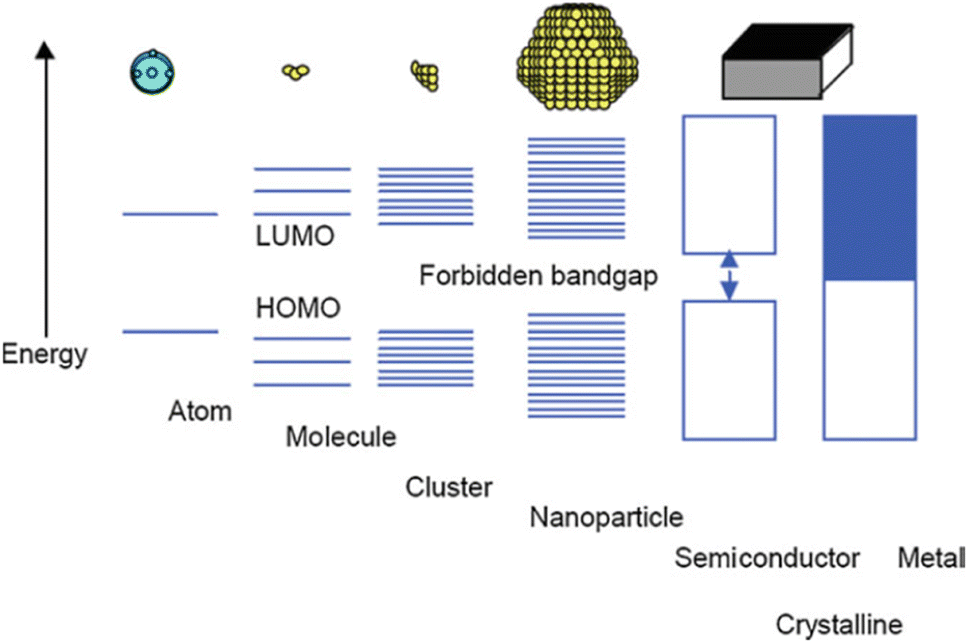 | ||
| Fig. 1 Size quantization effect pertaining to the transition of electronic states from the characteristics of bulk metal or semiconductor materials to those observed in small clusters. Reproduced from ref. 39 with permission from Springer Nature. | ||
The effect of quantum size results in the formation of plasmons, which are characterized by a high-density electron cloud on the metal surface nanoparticles. These plasmons exhibit natural frequency oscillation, absorbing incident energy or photons that match their natural frequency oscillation, thereby undergoing resonance and absorption of energy, a phenomenon known as surface plasmon resonance (SPR).41 In specific instances, the resonance of localized electrons occurs on individual metal nanoparticles, denoted as LSPR, whereas in another scenario, the resonance of localized electrons arises on a metal nanofilm, allowing dielectric charge movement in a planar direction, denoted as PSPR (Fig. 2).42
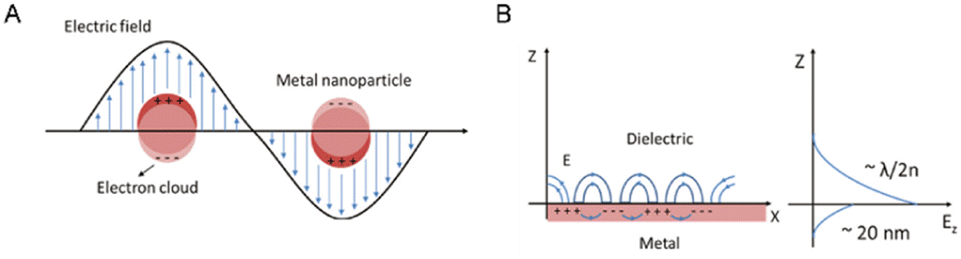 | ||
| Fig. 2 Schematic depiction detailing the occurrence of LSPR on a metal nanoparticle (A) and the interplay between electromagnetic waves and surface charges on PSPR (B). Reproduced from ref. 42 with permission from De Gruyter (CC BY-NC 4.0). | ||
Importantly, the SPR phenomenon extends beyond Au and encompasses various metal nanostructures, such as Ag, Cu, and Al. These metals have gained popularity in diverse applications, such as sensing, medical fields, and energy-related domains.43 The integration of AuNPs extends to various structural components in OSCs, including the hole-transport layer (HTL), active layer, buffer layer, and interfaces between each layer. Conversely, Au nanofilms or periodic metal nanopatterns were imprinted onto the top electrodes of OSCs. During light absorption in OSCs, the generation of excitons in organic semiconductors coincides with the induction of electric-field enhancements facilitated by plasmonic materials or structures. SPR in metal nanostructures (MNSs) engenders a repertoire of optical and electronic effects, manifesting during plasmon excitation and subsequent decoherence and ultimately contributing to enhanced photonic effects in OSCs.44
Plasmonic enhancement in solar devices is attributed to two primary mechanisms: (i) radiative effects, where SPR oscillates with incident light into the absorptive layer or MNSs function as a secondary light source, amplifying local electric fields; (ii) nonradiative effects, where SPR relaxes and the ensuing energy is transferred to the adjacent semiconductor, augmenting current generation. Notably, MNSs act as direct sensitizers during nonradiative processes. This section elucidates the four mechanisms of plasmonic enhancement (Fig. 3), encompassing light scattering (LS) and electromagnetic fields categorized as radiative effects, hot-electron transfer, and plasmon resonance energy transfer, which fall within the domain of nonradiative effects. Therefore, SPR can enhance exciton generation in organic semiconductors and improve the overall performance of OSC organic semiconductors.45
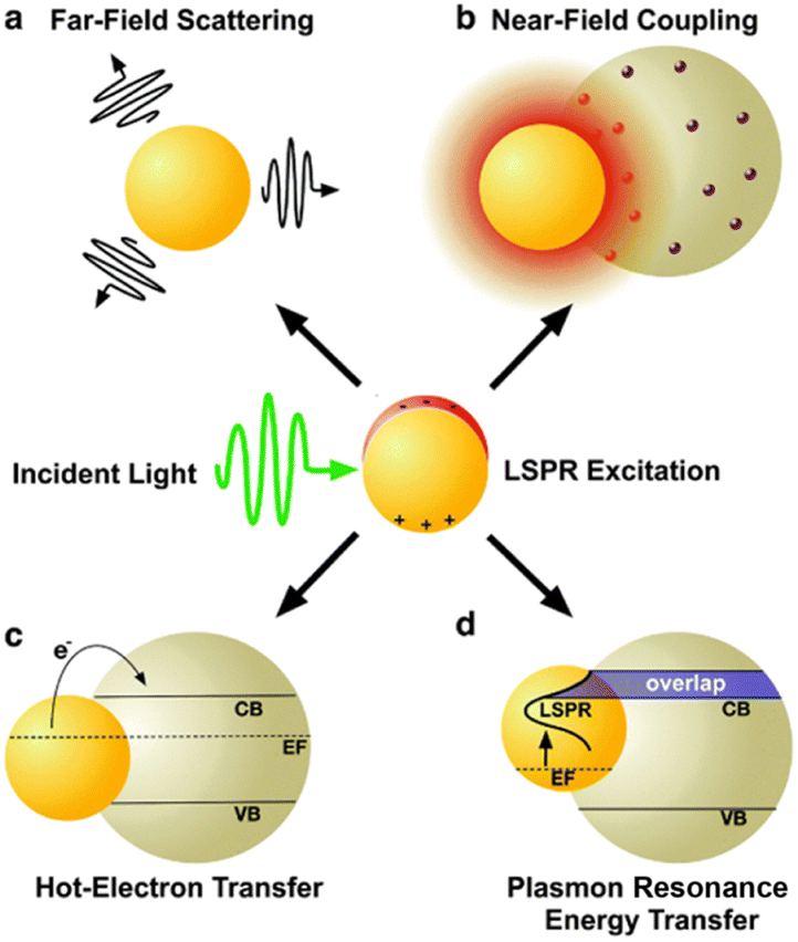 | ||
| Fig. 3 Schematic depiction of plasmon enhancement mechanisms, encompassing radiative effects such as (a) far-field scattering and (b) near-field coupling, as well as nonradiative effects such as (c) hot-electron transfer and (d) plasmon resonance energy transfer. Reproduced from ref. 45 with permission from the Royal Society of Chemistry (CC BY-NC 4.0). | ||
In the exploration of Au's spectroscopic properties, the reduction of AuNP size to atomic-cluster dimensions, specifically less than 2 nm, has been undertaken by wet chemical processes. Within the bandgap energy system, a distinct separation of the conductive and valence bands is evident, signifying the efficient utilization of photon energy for electron transition from the valence to the conductive band.46,47 Under electrical excitation, electron accumulation in the conductive band occurs, subsequently releasing excess energy to the valence band, leading to the emission of low-energy photons compared with the excitation energy, a phenomenon known as fluorescence. The resultant atomic-cluster Au particles were termed AuQDs. The reduction in the size of AuQDs induces varied energy levels within the conductive band owing to bandgap separation. The wavelength of the photons emitted from AuQDs is contingent upon their size; smaller particles exhibit higher emitted photon energy, intensity, and quantum yield than their larger counterparts.46,48 Although the fluorescence phenomenon of AuQDs has traditionally found applications in fluorescence sensors, they can also function as light-converting materials. This involves the harvesting of UV light to generate electron injection toward acceptor organic materials and the conversion of photon energy in the visible region for use in organic semiconductors (Fig. 4).2
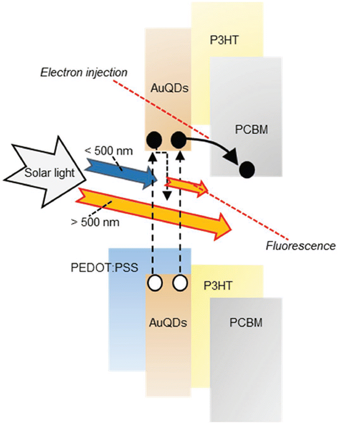 | ||
| Fig. 4 A schematic depiction of the proposed mechanism for photocurrent generation induced by AuQDs. Reproduced from ref. 2 with permission from John Wiley and Sons. | ||
3. Design strategies for fused OSC structures incorporating plasmonic AuNPs
OSCs with a sandwiched architecture comprising a bottom electrode, charge transport layer, bulk heterojunction (BHJ) active layer made up of mixed donor and acceptor materials, and top metallic electrode have been extensively developed. The incorporation of nanoparticles in devices can be categorized based on their position within the solar cell architecture. Plasmonic nanostructures of several sizes, shapes, and configurations have been introduced into the design of OSCs to tune the wavelength-dependent optical absorption characteristics of devices (Fig. 5).49 To improve the efficiency of OSCs, different configurations involving the incorporation of AuNPs within the hole transport or buffer layer,50 the photoactive layer51 on the ITO substrate52–54 or the interface of the charge transport layer/organic active layer55 have been investigated in the mainstream OSC design process. As a result, significant improvements in the efficiency of the corresponding device were achieved. The OSC efficiency enhancement can be attributed to several physical mechanisms.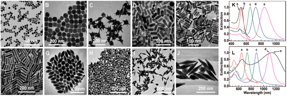 | ||
| Fig. 5 Representative TEM images of AuNPs of different shapes and sizes: (A) nanospheres; (B) nanocubes; (C) nanobranches; (D) nanorods (aspect ratio = 2.4 ± 0.3); (E) nanorods (aspect ratio = 3.4 ± 0.5); (F) nanorods (aspect ratio = 4.6 ± 0.8); (G) nanobipyramids (aspect ratio = 1.5 ± 0.3); (H) nanobipyramids (aspect ratio = 2.7 ± 0.2); (I) nanobipyramids (aspect ratio = 3.9 ± 0.2); (J) nanobipyramids (aspect ratio = 4.7 ± 0.2); normalized extinction spectra of AuNPs of different shapes and sizes. (K) Spectra (a)–(e) correspond to nanospheres, nanocubes, and nanorods with aspect ratios of 2.4 ± 0.3, 3.4 ± 0.5, and 4.6 ± 0.8, respectively. (L) Spectra (a)–(e) correspond to nanobipyramids with aspect ratios of 1.5 ± 0.3, 2.7 ± 0.2, 3.9 ± 0.2, and 4.7 ± 0.2, and nanobranches, respectively. Reproduced from ref. 49 with permission from the American Chemical Society. | ||
3.1 Metallic AuNPs embedded in the interfacial layer of OSCs
The incorporation of AuNPs at the interfacial layer between the anode or ITO substrate and the charge transport layer can enhance hole injection by reducing the potential barrier of the anode and hindering the quenching process of excited states in the polymer film.52 Moreover, LSPR in the vicinity of planar surfaces may be induced, resulting in improved OSC performance.55 Ren et al. investigated the insertion of gold nanostars (AuNSts, 70 nm) at the interface between the HTL (PEDOT:PSS) and the active layer (PBDT-TS1:PC71BM). Plasmonic asymmetric modes of AuNSts facilitate energy transfer so that the optical power in the electron transport layer is effectively transferred to the active layer, resulting in improved optical absorption. Simultaneously, plasmon-electrical effects were observed in the OSC, resulting in a more balanced flow of photogenerated electrons and holes from the active layer to the electrode. Additionally, the presence of AuNSts reduced the resistance of the HTL, achieving a significant PCE of 10.5% in the device.56Nagamani et al. introduced AuNPs into the interfacial layer of ITO/PEDOT:PSS and PEDOT:PSS/active layers to investigate the effects of AuNPs on OSC performance (Fig. 6(A–D)). The LSPR effect leads to improved absorption, increasing the percentage of light absorbed at the interfaces in devices incorporating gold nanospheres (AuNSs) (Fig. 6(B)). The presence of AuNSs also reduced the sheet and charge transport resistance at the interfaces (Fig. 6(C and D)), leading to an increased rate of exciton generation and dissociation. This enhancement contributes to a higher short-circuit current density (JSC) and an improved fill factor in the OSCs, ultimately resulting in a 16.1% improvement in efficiency.55 Furthermore, Notarianni et al. deposited Au layers, ranging in thickness from 1 to 5 nm, onto ITO substrates to investigate the potential enhancement in the PCE of OSCs. The plasmonic effect of Au islands (1 nm Au layers) resulted in increased scattering of photons into the active layer, leading to a 10% improvement in PCE compared with a control device.54 The integration of plasmonic gold nanodots (AuNDs), synthesized through thermally induced shape transformation of gold nanorods (AuNRs) on ITO substrates, was found to boost PCE from 3.04% to 3.65%. This improvement is attributed to the influence of the resultant plasmon field.57
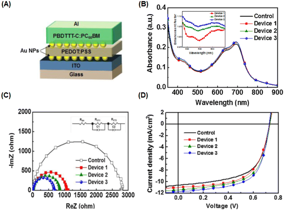 | ||
| Fig. 6 (A) Device structure of OSCs incorporating AuNPs as the interfacial layer; (B) absorbance spectrum of the PBDTTT-C:PC61BM film with AuNPs. The inset shows the absorption-enhancement factor of the interfacial AuNP-based device. (C) Electrochemical impedance spectroscopy results of the OSCs under one-sun illumination; (D) current density–voltage (J–V) curves for the PBDTTT-C:PC61BM (control) and incorporated AuNPs. AuNPs were deposited onto the PEDOT:PSS layer (device 1), ITO layer (device 2), and both layers (device 3). Reproduced from ref. 55 with permission from Elsevier. | ||
The modification of gold nanowires (AuNWs) as plasmonic antennae at the interface between PEDOT:PSS and ITO layers in the device resulted in a remarkable enhancement, boosting the photocurrent by 23.2% and efficiency by 11.4%. A reduction in the thickness of the spacer layer, enabling the extension of the evanescent field into the photoactive layer, as well as the geometry of the AuNW bands, which promotes enhanced scattering, played a significant role in achieving this improvement.53 Au nanomeshes were also introduced at the interface of PEDOT:PSS and ITO layers to induce plasmon excitation and far-field scattering in OSCs. Consequently, PCE increased from 1.9% to 3.2%.58
3.2 Metallic AuNPs embedded in the hole-transport layer of OSCs
Several researchers have investigated the dependence of LSPR on the size and concentration of AuNPs used and reported enhancements in the PCE of OSCs. Embedding plasmonic Au nanostructures into the buffer or HTL induces an optical effect that enhances light absorption in the active layer. This stimulates the rate of exciton generation.58 Possible ways of improving the light-trapping efficiency of OSCs include (i) the fluorescent light scattering (FLS) effect, which involves redirecting incident light into a thin photoactive layer to effectively increase the probability of photon absorption within the active layer, and (ii) the LSPR effect, which involves inducing near-field enhancement in the vicinity of plasmonic nanostructures within the active layer, leading to a corresponding increase in the effective absorption cross-section of the active layer (Fig. 7).59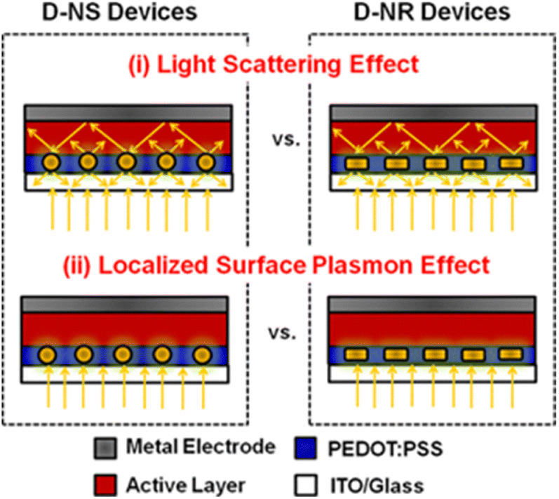 | ||
| Fig. 7 Schematic of two strategies for enhancing light trapping in PEDOT:PSS buffer layers: (i) FLS and (ii) LSPR effects. Reproduced from ref. 59 with permission from the American Chemical Society. | ||
Li et al. reported that the inclusion of decahedral-shaped AuNPs (∼32 nm) into the PEDOT:PSS of OSCs exhibited a high efficiency for OSCs based on P3HT:PC61BM and PBDT-TS1:PC70BM as photoactive layers, with maximum PCEs of 4.14% and 10.29%, respectively. The amplification of electric-field intensity can boost light absorption within the photoactive layer, increasing photocurrent production.60 Embedding AuNPs into PEDOT:PSS increases the density of excitons that align with resonance. AuNPs also provide high stability, a broader resonance peak, and surface resonance frequency dependence on the free electron density within the particle.50
3.3 Metallic AuNPs embedded in the photoactive layer of OSCs
The introduction of metallic nanoparticles to the active layers of OSCs leverages the highly confined field generated by LSPR, which enhances LS within the active layers.61 Furthermore, structural stability is enhanced by the dispersion of AuNPs into the photoactive layer, which reduces the device degradation rate during extended exposure to light. In such a case, higher light harvesting improves the initial cell efficiency, whereas enhanced structural stability contributes to superior device durability.62 The incorporation of 70 nm truncated octahedral AuNPs at an optimal concentration (5 wt%) into the BHJ active layer resulted in 4.36% PCE improvements in the P3HT:PC70BM system because of the enhancement of light absorption and charge transport in the developed devices.63 Jang et al. improved light utilization in OSCs by combining plasmonic AuNPs and a squaraine (SQ) dye in a photoactive layer, P3HT:PC61BM, resulting in a significant enhancement in PCE of approximately 36% (Fig. 8).64 The introduction of monofunctional PEG-capped AuNPs (0.5 wt%) into the active layer of the polymer blend, consisting of PFSDCN, resulted in a notable 32% PCE improvement.51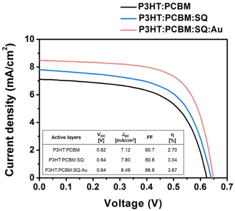 | ||
| Fig. 8 Current–voltage (J–V) curves acquired from OSCs comprising various active materials, including P3HT:PC61BM, P3HT: PC61BM:SQ, and P3HT: PC61BM:SQ:AuNSs. The photovoltaic parameters of the OSC devices shown are succinctly summarized in the inset table. Reproduced from ref. 64 with permission from Elsevier. | ||
3.4 Metallic AuNPs embedded in the non-fullerene acceptor of OSCs
Fullerene and its derivatives, such as PC61BM and PC71BM, are extensively utilized as electron acceptors in OSCs due to their high electron mobility and efficient charge transfer. However, traditional OSCs employing fullerene derivatives encounter limitations, yielding relatively low PCEs, typically around 11%.65,66 Thus, the development of non-fullerene acceptors (NFAs) signifies a significant milestone in the field. Recently, NFAs in OSCs have garnered substantial attention due to their favorable characteristics, including good electron mobility, tunable energy levels, and robust absorption across visible and NIR regions.19,65–67 Presently, PCEs exceeding 20% have been achieved, marking the highest reported PCE for non-fullerene OSCs.68,69 Efforts have focused on developing new photoactive materials with extended NIR absorption and employing strategies like MNSs for NIR absorption enhancement via LSPR.19,33,70Zhao et al. conducted a study to enhance the performance of non-fullerene OSCs utilizing PM6:Y6 by integrating hybrid plasmonic Au nanostructures (Fig. 9(A and B)). These nanostructures, comprising AuNSs with an LSPR peak at 520 nm and gold nanobipyramids (AuNBPs) with an LSPR peak at 820 nm, were embedded within the HTL consisting of PEDOT:PSS. By tailoring the cooperative LSPR of AuNBPs and AuNSs to match the absorption spectrum of the photoactive layer (PM6:Y6), a substantial enhancement in light absorption was achieved across a widened wavelength range, encompassing both visible and NIR regions in the OSCs. Compared to the control device lacking AuNSs or AuNBPs, the PCE of the PM6:Y6-based OSCs increased from 15.46% to 16.62%. This enhancement primarily resulted from the improved Jsc, which rose from 25.43 mA cm−2 to 26.53 mA cm−2. Additionally, enhanced External Quantum Efficiency (EQE) was observed, particularly in the visible and NIR regions, consistent with the excitation of LSPR induced by the resonance wavelength (Fig. 9(D)). The augmented optical and electrical properties were attributed to the strong near-field plasmonic enhancement and scattering effects, coupled with improved charge extraction and transport facilitated by the hybrid nanostructures embedded within the OSCs.19
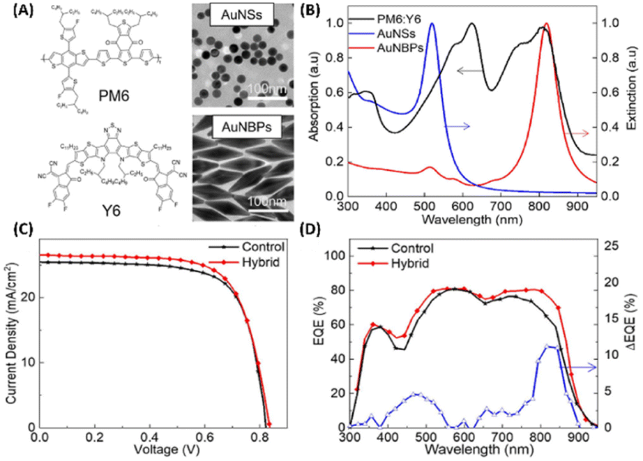 | ||
| Fig. 9 (A) The molecular structure of PM6:Y6 and TEM images of AuNSs and AuNBPs, (B) absorption spectrum of PM6:Y6 and extinction spectra of AuNSs and AuNBPs, (C) J–V characteristics of control devices and device with hybrid MNSs, and (D) EQE spectra and EQE difference between devices with and without hybrid MNSs. Reproduced from ref. 19 with permission from Elsevier. | ||
Furthermore, the investigation extended to exploring the efficacy of hybrid nanostructures in enhancing the performance of OSCs utilizing alternative non-fullerene photoactive layers, such as PBDBT:ITIC. Integration of AuNSs and AuNBPs resulted in a notable enhancement, yielding a PCE of 9.84%, surpassing that of the control device (9.17%). This improvement primarily stemmed from the augmented Jsc, mirroring the findings in PM6:Y6-based OSCs, thereby demonstrating the adaptability of hybrid plasmonic nanostructures in improving the efficiency of non-fullerene OSCs.19 Additionally, Xu et al. developed semitransparent (ST) OSCs employing a BHJ blend of PM6:BTP-eC9 as the photoactive layer. Integration of AuNBPs, exhibiting an LSPR peak at 825 nm, into the HTL of PEDOT:PSS within the device capitalized on the enhanced NIR absorption of the BTP-eC9 NFA within the BHJ layer. The combined enhancement in electrical properties, evidenced by reduced resistance compared to the control device, and the augmentation in NIR absorption attributed to AuNBP-induced LSPR, collectively contributed to the noteworthy performance of the ST-OSCs, achieving a high PCE of 13.15% (Fig. 10).70
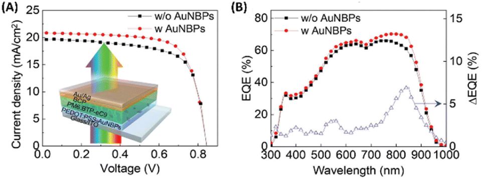 | ||
| Fig. 10 (A) J–V characteristics of the ST-OSCs, with and without AuNBPs; (inset) cross-sectional schematic view of the AuNBP-based ST-OSCs. (B) EQE spectra and EQE difference between devices with and without AuNBPs. Reproduced from ref. 70 with permission from John Wiley and Sons (CC BY-NC 4.0). | ||
4. Effect of AuNP morphology on OSC performance
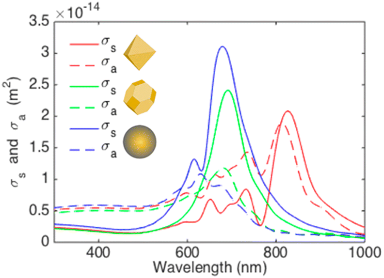
Plasmonic AuNPs with diameters ranging from 2 to 100 nm exhibit unique optical and physical properties, depending on their size and shape.37,50,71,72 AuNPs have been widely used to enhance photovoltaic performance because they are not subject to oxidation effects, thereby ensuring the durability of the device. The optical characteristics of AuNPs exhibit a redshift with an increase in the size of AuNSs.49 The influence of various sizes or shapes on the improvement of absorption in solar cells has been extensively investigated. Relatively small particles of AuNPs with dimensions of 5–20 nm, which are known to exhibit strong near-field coupling with excitons, have been widely used to incorporate them into organic photovoltaic devices.73,74 According to Mie theory, an increase in nanoparticle size or dimensionality results in a shift toward greater scattering than absorption. For smaller sizes with radii of less than 50 nm, the absorption efficiency is significantly higher than that of scattering.75 The inclusion of the plasmonic properties of AuNPs in a variety of morphologies has been widely reported.4.1 Spherical AuNPs
Spherical AuNPs or AuNSs have found extensive utility across diverse applications because of their intense and vibrant coloration coupled with a straightforward synthesis methodology. Predominantly endorsed in prior studies, the Turkevich method is recommended for generating AuNSs through the reaction between gold ions and citrate in a high-temperature solution.76 These AuNSs exhibit singular broadband light absorption spanning 500–600 nm, accompanied by nanoparticle size.76 By leveraging the plasmonic properties of AuNSs, they effectively harmonize with the light-absorption characteristics of semiconductor dyes in OSCs. Consequently, AuNSs persist as integral light-trapping materials in the realm of solar cell technology.Said et al. compared the effect of various particle sizes of AuNPs with diameters less than 23 nm (12, 14, 15, 17, 19, and 23 nm) on the efficiency of OSCs. Using UV-visible spectra (Fig. 11(A and B)), they revealed a shift in SPR toward longer wavelengths with increasing particle size. The presence of AuNPs of different sizes in the PEDOT:PSS film also enhanced the photovoltaic properties resulting from the localized surface plasmon effect of AuNSs. The efficiency increases as the particle size of AuNSs within the devices decreases because the inbuilt electric field around the small size is higher than that around the large size. AuNSs with small sizes (12 nm) produced greater efficiency, with a 24% improvement in OSCs based on CuPc/C60. The enhancement in light absorption could be attributed to an enhancement in the electric field at the interface between CuPc and C60, induced by the LSPR effect of AuNSs in PEDOT:PSS within the device.50
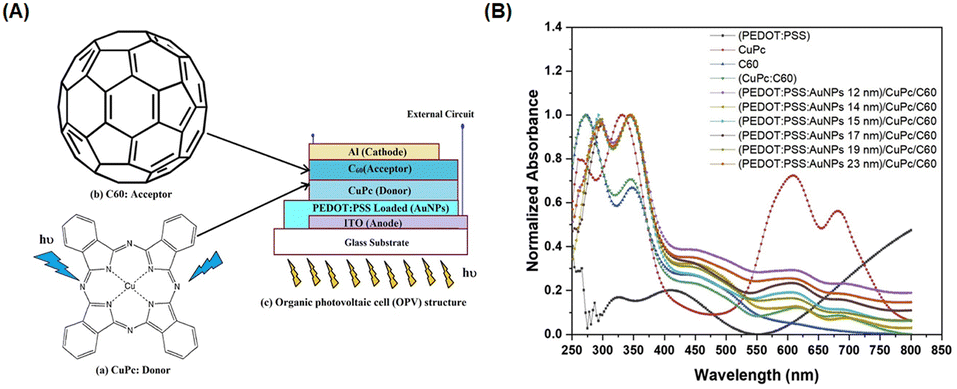 | ||
| Fig. 11 (A) Chemical structure of CuPc as a donor (a) and fullerene (C60) as an acceptor (b), and schematic structure of the organic photovoltaic cell (c); (B) normalized absorption spectra of CuPc, C60, and different sizes of AuNSs embedded in PEDOT:PSS/CuPc/C60 multilayer films. Reproduced from ref. 50 with permission from Elsevier (CC BY-NC 4.0). | ||
Chander et al. studied the optimal size of AuNSs (approximately 5, 17, 36, and 85 nm) for enhancing photocurrents in dye-sensitized solar cells and found that devices containing intermediate-sized AuNSs (∼36 nm) exhibited greater enhancement than those with larger or smaller AuNSs.77 Similar to the trend observed by Sarkar et al., AuNSs with a radius of approximately 30 nm can boost photocurrent by enhancing absorption. It notably attained a 16.89% increase in optical efficiency within OSCs.78 Furthermore, numerous studies have reported that the strongest localized electric field (near field) is produced by intermediate-sized AuNSs (with a diameter of approximately 40–50 nm).79,80 Furthermore, nanoparticles larger than 50 nm exhibit lower plasmon energy but function as far-field scattering entities in which photons undergo scattering in backward and forward directions, effectively extending the optical path length and enhancing absorption in various OSCs.81,82 Wang et al. reported that the use of larger AuNSs was associated with various positive effects in the P3HT:PC70BM system. These individual AuNSs can serve as effective hole conductors because their work functions are closely related to the energy level of the highest-occupied molecular orbital of P3HT. This alignment promotes more efficient hole transport within the system. The addition of truncated octahedral AuNPs (∼70 nm) to BHJ photovoltaic cells enhances the short-circuit current, fill factor, and IPCE, resulting in a 4.36% PCE improvement.63 Shin et al. investigated the role of larger-sized AuNSs, specifically those with a diameter greater than 70 nm, on OSC performance. They achieved this by embedding AuNSs with varying diameters of 71, 80, 87, and 103 nm into the PEDOT:PSS layer using two systems of donor/acceptor BHJs, PBDTTT-C:PC61BM and PTB7:PC71BM, to conduct the experiment (Fig. 12(A)). They suggested that near-field coupling LSPR was dominant for PEDOT:PSS doped with AuNSs smaller than 80 nm, whereas far-field scattering enhancement was prevalent in PEDOT:PSS containing AuNSs larger than 87 nm (Fig. 12(B–D)). By incorporating 87 nm AuNSs, remarkable PCEs of 5.35% and 8.58% were attained using PBDTTT-C:PC61BM and PTB7:PC71BM as BHJs, respectively. This improvement could be attributed to the balanced contribution of near- and far-field plasmonic effects, along with improved vertical coverage and enhanced interfacial properties. They also showed that the largest size of AuNSs that can achieve a higher efficiency is 87 nm, above which the rate of improvement drastically decreases.82
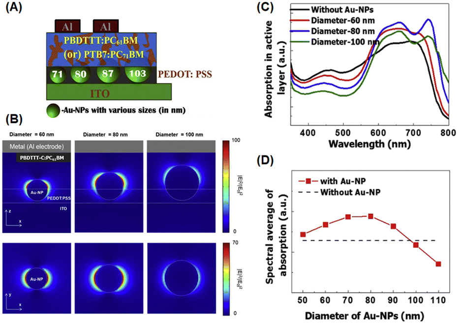 | ||
| Fig. 12 (A) Graphical representation of AuNSs of different sizes (71, 80, 87, and 103 nm) in PEDOT:PSS with PBDTTT-C:PC61BM or PTB7:PC71BM BHJ (100 nm); (B) simulated optical absorption enhancement by AuNSs; (C) calculated electric-field intensity (λ = 740 nm) around AuNSs with diameters of 60 nm (left), 80 nm (middle), and 100 nm (right) in the xz- (top) and xy-planes (bottom); the optical absorption spectra of the PBDTTT-C:PC61BM layer with (red, blue, and green lines) and without AuNSs (black line). In the presence of AuNSs, their diameters were 60 nm (red), 80 nm (blue), and 100 nm (green). (D) Spectral average of optical absorption in the active layer with (red symbols) and without AuNSs (black dashed line). Reproduced from ref. 82 with permission from Elsevier. | ||
4.2 Gold nanorods
Intriguingly, the specific geometry of plasmonic nanoparticles plays a crucial role in their properties, directly influencing SPR and the scattering of incident light. Most studies emphasized the use of AuNPs with spherical shapes.25 However, sharp edges can substantially enhance the local field intensity while introducing strong parasitic absorption.75 Gold nanorods (AuNRs) have also been widely incorporated into OSCs because of their capability for extensive tunability of SPR wavelengths, extending from the visible to NIR regions, which can be achieved through simple modifications of their aspect ratios.83,84 AuNRs exhibit greater plasmonic characteristics than other AuNPs of different shapes, and they exhibit two LSPR modes consisting of transverse and longitudinal modes. Generally, the plasmonic properties of AuNRs are directly proportional to their aspect ratio. The longitudinal dipole plasmon wavelength increases linearly from the visible to the mid-infrared range as the length-to-diameter aspect ratio increases, significantly enhancing the electromagnetic field at the ends and extraordinarily large extinction cross-sections. Moreover, the ability to scatter more incident photons increases with diameter. A reduction in the size of AuNRs corresponds to a decrease in their aspect ratio.28,85The introduction of AuNRs into the photoactive layer is associated with an increase in light-harvesting properties, which leads to a higher PCE of the device.86,87 The inclusion of AuNRs in inverted OSC-based PCDTBT and PC71BM exhibited an enhancement of PCE of 6.83%, representing an 18.9% improvement.88 The aspect ratio and concentration of AuNRs significantly influence and improve photovoltaic performance.89 The effect of loading concentrations (1% and 2% Au/P3HT by weight) of various sizes of AuNRs with aspect ratios of 2.15, 2.50, and 3.30 (average lengths/widths were 38/18, 43/18, and 49/15 nm, respectively) on OSC efficiency was studied by Wadams et al.89 Transverse resonance bands appeared at approximately 530 nm, whereas longitudinal resonance bands occurred at longer wavelengths (approximately 638, 685, and 780 nm). As the aspect ratio of the embedded AuNRs increased, there was an induced increase in extinction. The most notable efficiency boost, approximately 30% enhancement, was obtained when AuNRs with an aspect ratio of 3.30 at a concentration of 2 wt% were incorporated into the P3HT:PC61BM film.
Lui et al. demonstrated enhanced OSC performance based on PTB7-Th:PC71BM by adding a mixture of AuNRs to the device.90 Hydrophilic and hydrophobic AuNR mixtures (containing AuNRs with lengths of 23, 35, and 47 nm) were loaded into the HTL (PEDOT:PSS) and active layer (PTB7-Th:PC71BM). The results showed that the use of complementary plasmonic AuNR mixtures broadened the LSPR wavelength range response in OSCs and slightly improved charge dissociation, significantly improving the short-circuit current density from 16.3 to 17.9 mA cm−2 with a high PCE of 10.31%. The addition of optimized Au–silica core–shell nanorods (1 wt%) into the photoactive layers of the OSCs enhanced PCE by increasing light absorption and LS within the devices. Xu et al. investigated two different photoactive materials, P3HT:PC61BM and PCPDTBT:PC70BM polymer blends.91 In the case of P3HT:PC61BM, the absorption spectrum only overlapped with one of the plasmon resonance peaks of the Au–silica nanorods. The efficiency of the device was enhanced by 12.9%, from 3.17% to 3.58%. In contrast, the absorption spectra of PCPDTBT:PC70BM were relatively broad and corresponded to the two plasmon resonance peaks of Au–silica nanorods. This resulted in a substantial efficiency improvement of 26%, increasing from 3.50% to 4.40%. The surface morphologies of Au–silica nanorods with different loading concentrations on PCPDTBT:PC70BM were explained with the help of atomic force microscope (AFM) images (Fig. 13).91
 | ||
| Fig. 13 AFM images of the PCPDTBT:PC70BM film: (A) the film without Au–silica nanorods, (B) the film with 1 wt% and (C) the film with 2 wt% Au–silica nanorod concentrations. Reproduced from ref. 91 with permission from Elsevier. | ||
Furthermore, the interfacial layers of the contact materials play a crucial role in improving the efficiency of OSC devices by modifying the metal work function of the contact and enhancing the selectivity of a specific charge carrier.28 Based on the PTB7:PC71BM blend, a strategy involving the placement of AuNRs as rear interfacial modifiers close to the photoactive layer resulted in a significant improvement in the PCEs of the OSCs, exceeding 8%. This enhancement in light absorption was induced by the highly efficient scattering of AuNRs and strong near fields generated by the LSPR effect of AuNRs partially protruding inside the photoactive layer.84 Interestingly, the integration of polyelectrolyte PSS-coated plasmonic AuNRs (AuNRs@PSS) as rear interfacial modifiers between the photoactive and back-contact HTL in inverted non-fullerene OSCs demonstrated an increase in light trapping and charge generation within the device. AuNRs exhibit the dual function of accelerating charge generation through the near-field SPR effect and enhancing photon reabsorption through the backscattering effect. The uniform distribution of AuNRs on the surface was supported by the ultrathin PSS shell, which improved interface contact and facilitated hole transport from the photoactive layer to HTL. These synergistic effects significantly enhanced photovoltaic performance, achieving a major increase in Jsc of 21.34 mA cm−2 and a high efficiency of 10.11%, representing an enhancement of approximately 20% compared with the control device.83
Hsiao et al. also investigated the enhancement of the light-trapping efficiency of OSCs by the incorporation of AuNSs and AuNRs of different sizes and shapes into PEDOT:PSS. Fig. 14(A–E) show the TEM images and extinction spectra of AuNSs and AuNRs of various sizes. This figure shows the diverse LSPR properties of AuNPs of different sizes and shapes over a wide spectral range from visible to NIR. The tunable LSPR band positions of 520, 530, 540, 660, 780, and 850 nm obtained from these AuNPs (NS520, NS530, NS540, NR660, NR780, and NR850, respectively) could enhance the light-trapping efficiency of OSCs. AuNSs with a diameter of approximately 50 nm (NS540) exhibited an excellent ability to concentrate light, effectively harnessing short-wavelength visible light through LS and LSPR effects in photovoltaic devices. This improved the OSC performance by approximately 4.1% with a 17% enhancement (Fig. 14(F–G)). The near-field enhancement, which prevents the recombination of geminate excitons, increases the exciton dissociation rate at the active layer and enhances the efficiency of the device. They also mixed optimal AuNSs and AuNRs into PEDOT:PSS to activate multiple LSPR bands. Consequently, an improvement of approximately 24% in PCE was achieved compared with the reference device (ITO/PEDOT:PSS/P3HT:PCBM/Ca/Al).59
 | ||
| Fig. 14 TEM images of AuNPs of different sizes and shapes: (A) NS540, (B) NR660, (C) NR780, and (D) NR850; (E) normalized UV-vis-NIR extinction spectra of Au NPs of various sizes and shapes in aqueous solutions; OSC performance under AM 1.5G illumination (100 mW cm−2): (F) current–voltage (J–V) characteristics and (G) EQE spectra. Reproduced from ref. 59 with permission from the American Chemical Society. | ||
4.3 Gold nanostars
Distinct three-dimensional nanostructures, including stars, urchins, and durians, with numerous thorn structures on their surfaces emerge through anisotropic growth under the influence of weak reducing agents and specific capping agent conditions.92 These intricate structures, which result from such growth parameters, exhibit plasmonic coupling, resulting in a wide spectrum of light absorption and scattering spanning the visible to the NIR region.93 Gold nanostars (AuNSts),30 urchin-like AuNPs (UL-AuNPs),1 and spiky durian-shaped AuNPs94 have been documented for their efficacy in light-trapping applications in OSCs. In particular, thorn nanostructures can increase the electric field and light scattering, contributing to the enhanced efficiency of OSCs.1Pangdam et al. elucidated an enhancement in OSC performance using a specific N/P-type structure (ITO/PEDOT:PSS/P3HT:PC61BM/Al) (Fig. 15(A)). Urchin-like AuNPs (UL-AuNPs) were synthesized via seed-mediated growth from AuNSs assisted by silver ions. The UL-AuNPs exhibited an average size of approximately 60–80 nm, with a maximum absorption wavelength of 730 nm. The high dispersion of UL-AuNPs in water, blended in PEDOT:PSS within the concentration range of 0.00–0.09 mM, revealed optimal enhancement at 0.05 mM, resulting in a 3.3% improvement in OSC performance and a 5.86% overall enhancement. Finite-difference time-domain (FDTD) simulations underscored superior electric-field enhancements of UL-AuNPs to their spherical counterparts (Fig. 15(B–D)).1
 | ||
| Fig. 15 (A) A schematic representation of the simulated structure and electric-field intensity maps in OSCs, comparing those integrated with UL-AuNPs on the right and AuNSs on the left. The electric-field intensity was analyzed at irradiation wavelengths of (B) 700, (C) 560, and (D) 450 nm. Reproduced from ref. 1 with permission from the Royal Society of Chemistry. | ||
Moreover, Ren et al. previously reported the efficacy of anisotropic gold nanostructures for enhancing OSCs. AuNSts with an average particle size of 70 nm were spin-coated between the cathode and HTL in the ITO/PEDOT:PSS/PBDT-TS1:PC71BM/Ca/Al photovoltaic model. Remarkably, AuNSts reduced the resistance of the HTL, leading to a commendable power conversion efficiency of 10.5% achieved through the cooperative plasmon-optical and plasmon-electrical effects of AuNSts.56
Ren et al. demonstrated the efficacy of AuNSts in significantly enhancing the performance of inverted OSCs and perovskite solar cells through the surface immobilization of gold (Fig. 16(A and B)). In the OSC scenario, mPEG-thiol was a nonpolar modification agent for 35 nm-sized AuNSts and was transferred to a chlorobenzene (CB) solution (Fig. 16(A and B)). These modified AuNSts were subsequently integrated into the active layer at loading concentrations of 0.01, 0.03, and 0.12 wt% within the photovoltaic model of ITO/ZnO/PTB7:PC61BM/PEDOT:PSS/Ag. The results revealed an 8.78% improvement in OSC performance and an overall enhancement of approximately 6% when the AuNSt loading concentration was 0.01 wt%. This shows that the robust electric field generated by AuNSts facilitated efficient charge separation within the active layers of OSCs. The observed electrical enhancements are attributed to reduced charge recombination rates and accelerated charge transport in OSCs upon the incorporation of AuNSts.56
 | ||
| Fig. 16 Illustration of typical configurations of devices, delineating the placement of AuNSts (or Au NSs in this figure) in (A) inverted OSCs and (B) planar-based perovskite solar cells. (C) TEM image showing the dispersion of AuNSts in CB solution, with the inset providing a magnified view of a single AuNSt. (D) Optical absorption spectra of AuNSts, comparing those with and without mPEG-SH modification; the inset of (D) displays the dispersions of AuNSts with and without mPEG. Reproduced from ref. 30 with permission from the American Chemical Society. | ||
4.4 Gold quantum dots
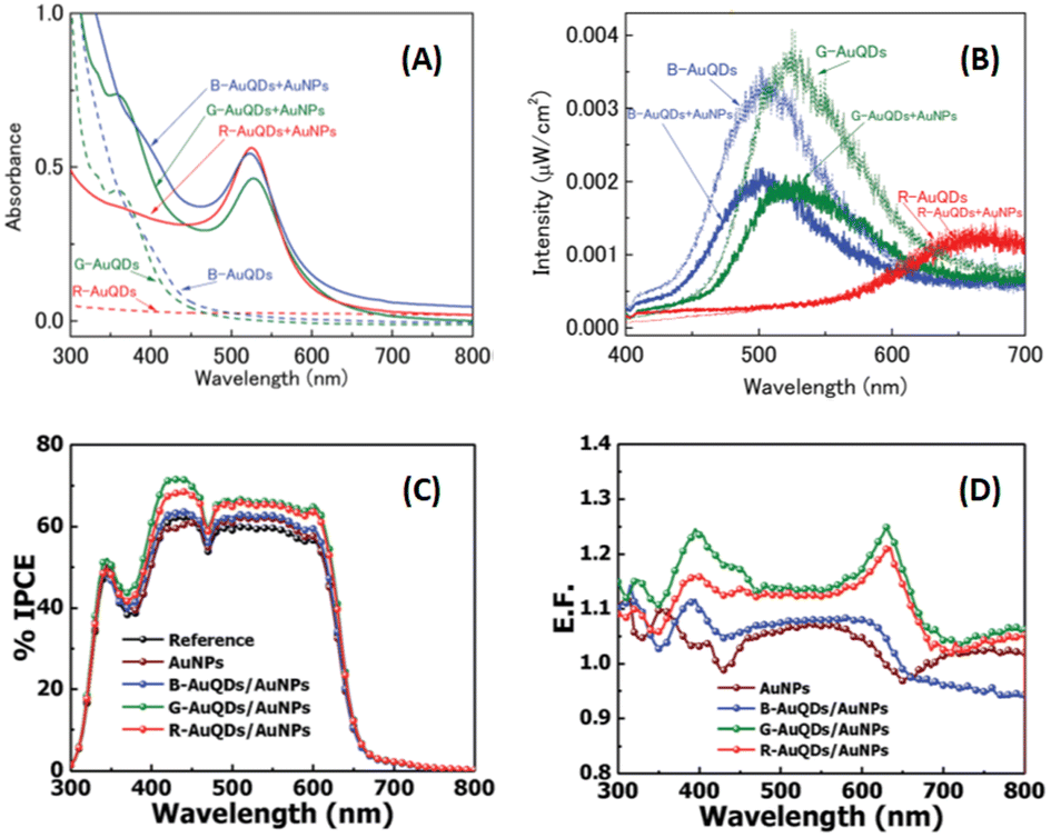
Au particles with diameters of less than 2 nm are referred to as AuQDs or Au nanoclusters, and they cannot support localized surface plasmons. Instead, AuQDs exhibit quantum confinement effects, where the fluorescence emission wavelength in the visible range is determined by the number of Au atoms within the clusters.95 The excitation of electrons in AuQDs occurs because of near-UV light absorption, propelling them from the ground to the excited state. The use of AuQDs in photoelectric conversion systems was first introduced by Tatsuma and colleagues.96 In their seminal work, AuQDs were used as photosensitizers on TiO2 electrodes to facilitate light harvesting across the visible to NIR spectrum. Moreover, AuQDs have been instrumental in enhancing the performance of dye-sensitized solar cells, extending the harvesting wavelength and broadening the absorption region of the dyes.Pangdam et al. highlighted the exceptional properties of AuQDs by exploiting their distinctive light emissions with maximum peaks at 507 nm (B-AuQDs), 520 nm (G-AuQDs), and 650 nm (R-AuQDs). These AuQDs were incorporated into the HTL in the photovoltaic model of ITO/PEDOT:PSS/P3HT:PC61BM/Al (Fig. 17(A)). The AuQD concentrations ranged from 1.00 to 4.00 μM and were directly dispersed in the HTL as a water-soluble phase. These results underscore the light-converting efficiency of AuQDs in harnessing photon energy beyond the absorption range of semiconductor dyes, extending into the UV region. Notably, among the AuQDs, G-AuQDs at a loading concentration of 3.00 μM emerged as the most impactful, yielding a substantial 3.59% improvement in OSC performance and an overall enhancement of 10%. Both fluorescence and plasmonic enhancements were quantitatively evaluated in the broad band of visible light regions through FDTD simulations (Fig. 17(B–D)), corroborated by IPCE and enhancement factor (E. F.) analyses (Fig. 17(E and F)).2 Furthermore, by leveraging gold particles, the in situ generation of aggregated gold particles was explored to enhance plasmonic effects in OSCs, as evident from AFM images (Fig. 18).2
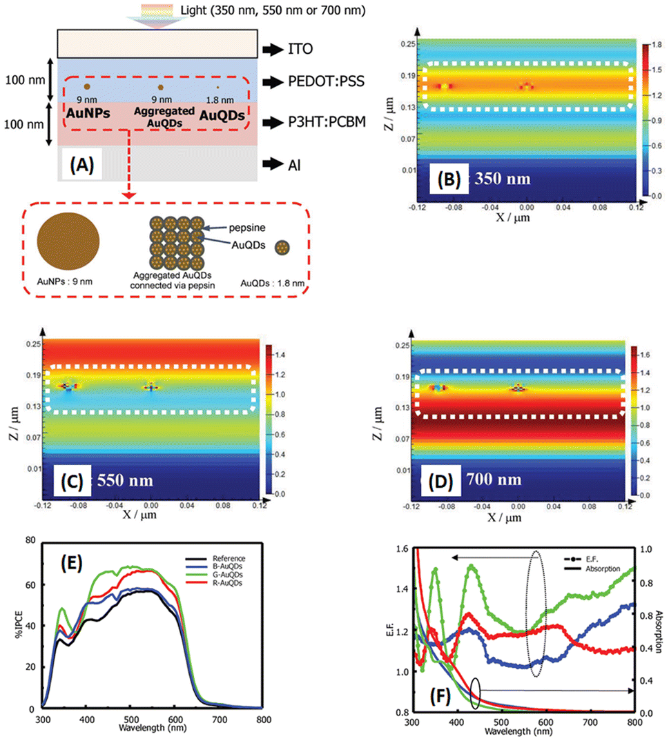 | ||
| Fig. 17 Schematic representations (A–D) of simulated structures, featuring (A) the overall structure and electric-field intensity maps of OSCs incorporating AuNPs with a diameter of 9 nm, aggregated AuQDs with an aggregated size of 9 nm (where AuQDs with diameters of 1.8 nm are connected via pepsin molecules), and individual AuQDs with a diameter of 1.8 nm embedded in the PEDOT:PSS layer. These visualizations are presented under illumination at wavelengths of (B) 350, (C) 550, and (D) 700 nm. (E) The IPCE and (F) the enhancement factor (E. F.) spectra. Reproduced from ref. 2 with permission from John Wiley and Sons. | ||
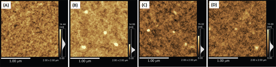 | ||
| Fig. 18 AFM images of (A) the PEDOS:PSS film, and (B) the B-AuQD-loaded, (C) the G-AuQD-loaded, and (D) the R-AuQD-loaded PEDOT:PSS film. The white spots in (B–D) indicate the domains of aggregated AuQDs. Reproduced from ref. 2 with permission from John Wiley and Sons. | ||
4.5 Mixing different shapes of AuNPs
Achieving precision control in the synthesis of AuNPs is pivotal in photonic and plasmonic materials because their plasmonic properties are inherently tied to morphology. An alternative approach involves plasmonic tuning by combining diverse morphologies within plasmonic materials. For instance, the integration of various shapes and sizes of silver nanoprisms (AgNPrs) imparts a plasmonic excitation that can generate a broad spectrum of light absorption, surpassing that achieved by individual AgNPr shapes. Notably, complex morphologies of AgNPrs, as opposed to simpler ones, have demonstrated enhanced efficacy in OSCs, underscored by their ability to produce multiple plasmonic excitations, thereby improving OSC efficiency.97 The concept of morphological mixing has been recurrently reported in the context of AuNPs for OSC applications.Kozanoglu et al. investigated the effect of different shapes of Au nanostructures, consisting of AuNSts, AuNRs, and AuNSs, on the efficiency of devices (Fig. 19(A–D)). Among these AuNPs, AuNSts exhibited the highest PCE because of the superior optical properties of AuNSts, including LS and LSPR effects, to AuNRs and AuNSs.98 Using anisotropic non-spherical nanoparticles instead of their spherical counterparts can reduce the ratio of absorption loss to scattering and enhance LSPR.60 AuNSts offer an advantage because of their sharp edges and complex geometries, resulting in many beneficial effects. These include LSPR generated by the core and spines, as well as enhanced LS from the branched edges and corners. Plasmonic asymmetric modes of AuNSts facilitate energy transfer, which significantly increases absorption inside the active layer.56 The PCE of OSCs by incorporating AuNSts in the photoactive layer (PTB7:PC71BM) was significantly improved by 6% because of the enhancement of optical and electrical properties that improved the short-circuit current density and fill factor in the device.30
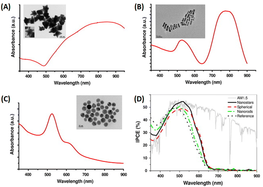 | ||
| Fig. 19 UV-vis absorption spectrum of (A) AuNSt, (B) AuNR, and (C) AuNS colloids in an aqueous medium. The inset is the TEM image. IPCE spectra of AuNP devices along with the air mass 1.5 reference solar spectral irradiance at global tilt (D). Reproduced from ref. 98 with permission from Elsevier. | ||
Ng et al. introduced AuNPs of different shapes, including gold nanocubes (AuNCs), AuNSs, and AuNRs, into the PEDOT:PSS buffer layer (Fig. 20). Consequently, the PCEs of the devices incorporating AuNPs exhibited significant enhancements, in which PCEs increased from 7.5% (control device) to 8.0%, 8.1%, and 8.2% for the devices containing AuNSs, AuNRs, and AuNCs, respectively. The most substantial improvement in PCE is shown in devices with AuNCs, which is attributed to the light-absorption enhancement across a wide wavelength range from 400 to 700 nm.99
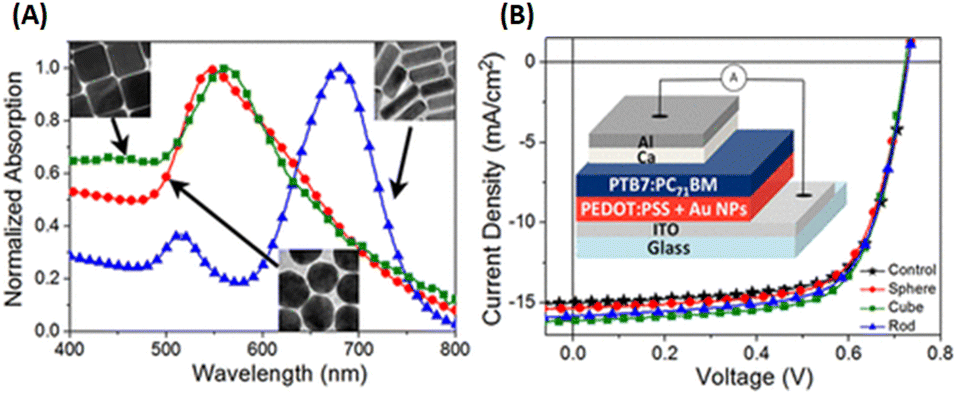 | ||
| Fig. 20 (A) Normalized absorption spectra of the PEDOT:PSS layer blended with different AuNPs. Inset: TEM images of AuNSs, AuNRs, and AuNCs. (B) J–V curves of OSCs incorporating different AuNPs. Inset: Device architecture of the PTB7:PC71BM-based plasmonic solar cell. Reproduced from ref. 99 with permission from the American Chemical Society. | ||
Arinze et al. simulated a model involving different shapes of AuNP systems consisting of octahedral AuNPs, truncated octahedral AuNPs,100 and AuNSs with the same size (70 nm) incorporated within PCDTBT:PC70BM (Fig. 21).100 The simulation results show that the truncated octahedral AuNPs have a more similar shape to AuNSs, whereas the octahedral AuNPs have noticeable sharp edges. Compared with the AuNSs, the truncated octahedral AuNPs exhibit a slight redshift and a decrease in the peak amplitude of the scattering cross-section. In contrast, the octahedral AuNPs show diminished scattering amplitudes and increased absorption, accompanied by a considerable redshift compared with the other particle variations. Within the spectral range of 300–800 nm, the absorption cross-section of the octahedral AuNPs surpasses their scattering cross-section, suggesting that this particle shape may not significantly enhance absorption within a PCDTBT:PC70BM film. The truncated octahedral AuNPs and AuNSs exhibit scattering cross-sections exceeding their absorption cross-sections, particularly near a wavelength of 700 nm. This implies that both types of nanoparticles can enhance photovoltaic absorption in this specific spectral range.
 | ||
| Fig. 21 Scattering (solid lines) and absorption (dashed lines) cross-sections vs. wavelength for different shaped plasmonic nanoparticles of similar size embedded in a PCDTBT:PC70BM background. Red: 70 nm octahedral AuNPs. Green: 70 nm truncated octahedral AuNPs. Blue: 70 nm AuNSs. Reproduced from ref. 100 with permission from the American Chemical Society (CC BY-NC 4.0). | ||
Liu et al. also investigated the effect of plasmonic resonances by embedding two types of plasmonic Au nanostructures in an OSC. Octahedral AuNPs (50 nm) were incorporated into PEDOT:PSS, whereas AuNDs (5.3 nm) were deposited on the photoactive layer (P3HT:PC61BM). Adding larger AuNPs resulted in increased scattering, which further expanded the optical path in the active layer, boosting light absorption and device performance. Additionally, the smaller AuNDs contributed to the light absorption in the device through their near-field effects. A dual Au nanostructure system can significantly enhance PCE to 4.8% with approximately 20% improvement compared to the conventional cell.101 Furthermore, Abhijith et al. explored the synergistic plasmonic effects of multi-shaped Au nanostructures positioned on WS2 nanosheets to enhance the photocurrent of fullerene- and non-fullerene-based OSCs.22 Various shapes of Au nanostructures, including spheres, cubes, ellipsoids, rods, prisms, and trapezoids, each with a diameter or edge length of approximately 50 nm, were hybridized with a few layers of WS2 nanosheets, forming Au–WS2 nanohybrid structures. The incorporation of Au–WS2 nanohybrids as an interlayer between PEDOT:PSS and photoactive layers enhanced the light-harvesting capability of OSCs across a broad wavelength range of 350–700 nm, achieving a significant PCE increase of 12.41%.
An enhancement induced by synergistic plasmonic effects, such as scattering efficiency, direction-dependent scattering, and near-field effects generated by various Au nanostructures, was confirmed through FDTD simulations. Each Au nanostructure presented unique near-field effects, which significantly enhanced field intensity within the active layer. Additionally, more than 50% forward scattering occurred, making these plasmonic nanostructures suitable for enhancing photosensitivity and increasing absorption density in the system.22 Loading mixed AuNPs, composed of bone-like rod shapes, cubes, and irregular spheres, into the PEDOT:PSS layer significantly improves the photovoltaic performance of the PTB7:PC71BM-based solar cell by 9.26%. The mixed AuNPs contributed to a broad absorption range of 350–1000 nm, resulting in increased absorption in the active layer. Additionally, AuNP doping decreased the bulk resistance of PEDOT:PSS, facilitating exciton dissociation, hole transport, and collection in the system.102
As mentioned above, the particular geometry and size of AuNPs embedded in OSCs significantly affect the efficiency of solar devices. The plasmonic activity could be turned on by the collaboration of various morphologies of AuNPs. As previously mentioned, OSC augmentation was achieved through the synergistic effects of aggregated AuQDs, incorporating plasmonic and fluorescence mechanisms. Phetsang et al.37 investigated these effects harnessed through the simultaneous utilization of AuQDs and AuNSs. These were strategically loaded at the cathode/HTL interface and blended within the HTL in the photovoltaic model of ITO/PEDOT:PSS/P3HT:PC61BM/Al. AuNSs with a concentration of 0.10 mM and an average size of 5.0 nm were incorporated into the PEDOT:PSS solution. Simultaneously, B-, G-, and R-AuQDs were spin-coated onto the ITO substrate at concentrations ranging from 1.2 to 10 μM. The fluorescence effect of AuQDs played a pivotal role in enhancing the near field around AuNSs, as evidenced by the reduction in fluorescence intensity observed in AuQDs and AuQD:AuNP aqueous solutions (Fig. 22(A and B)).37
 | ||
| Fig. 22 (A) UV-visible absorption spectra and (B) fluorescence spectra of AuQDs and AuQD:AuNP aqueous solution; (C) %IPCE and (D) E. F. profiles for OSCs incorporating AuQDs and plasmonic AuNPs. Reproduced from ref. 37 with permission from the Royal Society of Chemistry (CC BY-NC 4.0). | ||
Remarkably, G-AuQDs/AuNPs, with an AuQD-loading concentration of 3.00 μM, emerged as the most impactful, resulting in a significant 3.66% improvement in OSC performance and an overall enhancement of 13.0%. Incorporating AuNPs into PEDOT:PSS or the HTL increased the absorption possibilities within the photoactive layer, augmenting the exciton generation rate and the probability of exciton dissociation. Additionally, the fluorescence emission of AuQDs, contingent on the quantum size effect, enhances light harvesting from the UV region and generates specific fluorescence emissions within the fabricated devices, as substantiated by % IPCE and E. F. analyses (Fig. 22(C and D)).37 Incorporating an AuQD layer enhances photocarrier generation in the device through its fluorescence characteristics. Photogenerated carriers in the P3HT:PC61BM layer arise from UV and visible light absorption and fluorescence emission in the AuQD layer. Furthermore, combining AuQDs with AuNPs further boosts photocarrier generation, potentially facilitated by intensified localized plasmon fields at the AuNPs induced by AuQD fluorescence emission and energy/electron transfer from AuQDs to AuNPs which correspond to fluorescence quenching (Fig. 22(B)).
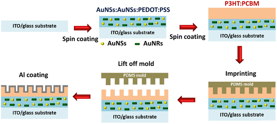
5. Dual gold nanostructures/quantum dots with metallic nanopatterns
To achieve higher PCEs in OSCs, enhancing light trapping in the active layer without increasing thickness would be desirable. This approach is crucial because carrier recombination increases when the active layer is thicker.101 To manage more light harvesting, the efficiency of OSCs has been significantly improved with the incorporation of periodic plasmonic nanostructures on the active layer that induce PSPR modes, leading to an enhancement of optical absorption and a remarkable improvement in the photocurrent in OSCs.103 The imprinting technique employed polydimethylsiloxane (PDMS) as a soft mold to replicate nanopatterns from a hard template. This soft mold was applied to the active layer of the OSCs. Under controlled temperatures, the transformation of organic semiconductors from a solid to a fluid state within the PDMS soft mold occurred. Subsequently, the organic semiconductors regained their solid state upon temperature reduction, thereby preserving the nanopatterns. After the metal coating was used as the top electrode, the PDMS soft mold was removed, revealing a rainbow effect owing to incident light reflection on the nanopatterned top electrode. Furthermore, nanopatterns on the top electrodes of OSCs enhance light diffusion, thereby increasing photocarrier generation.104In our reports, GCSPR,78,105–108 dual or multiple SPR-based GCSPR-integrated AuNPs,73 and AuQDs37,109 were demonstrated to significantly enhance the photocurrent in OSCs. The LSPR and GCSPR of hybrid plasmonics generally exhibit manifest characteristics and narrow resonance wavelength regions, which could broaden light absorption within photovoltaic devices. Phetsang et al. demonstrated the integration of LSPR via AuNSs with AuNRs and PSPR using an aluminium grating nanostructure. AuNPs with AuNRs were incorporated into the HTL, and the grating nanostructure, replicated from the BD-R grating pattern, was imprinted on the active layer in the ITO/PEDOT:PSS/P3HT:PC61BM/Al photovoltaic model (Fig. 23). Simultaneous use of LSPR from AuNSs and AuNRs, along with GCSPR, yielded a substantial 3.65% enhancement in OSC performance and an overall improvement of 14.06%. Diverse LSPR bands between AuNSs and AuNRs contributed to expanded light absorption, whereas GCSPR induced electric-field enhancement and LS in OSCs. Consequently, the synergistic interplay between LSPR and GCSPR significantly improved the optical properties.73
 | ||
| Fig. 23 Schematic representation of the fabrication process of hybrid plasmonic OSCs integrated with a metallic grating nanostructure. Reproduced from ref. 73 with permission from Taylor & Francis. | ||
Phetsang et al. investigated the coupling of fluorescence phenomena from AuQDs with GCSPR by expanding the imprinting technique to novel materials. AuQDs with green emission at 520 nm or G-AuQDs were dispersed in the HTL, and a grating nanostructure, replicated from the BD-R grating pattern, was imprinted on the aluminium layer in the photovoltaic model of ITO/PEDOT:PSS/P3HT:PC61BM/Al. Despite the strong PSPR in the 650–800 nm range not being aligned with P3HT:PC61BM, the near-field effects from GCSPR and the fluorescence of G-AuQDs impact IPCE enhancement across a broadband spectrum from 400 to 800 nm (Fig. 24). The combined use of fluorescence from G-AuQDs, the grating pattern, and GCSPR resulted in a substantial 3.91% enhancement in OSC performance, culminating in an overall improvement of 19.57%.110
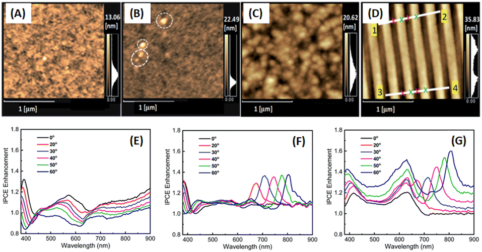 | ||
| Fig. 24 AFM images of HTL films prepared from (A) PEDOS:PSS and (B) G-AuQD-loaded PEDOT:PSS. The white circles in (B) indicate the domains of aggregated G-AuQDs. AFM images of the (C) flat and (D) BD-R imprinted photoactive layers. (E–G) Spectra depicting the enhancement of IPCE for green-AuQD/BD-R OSCs under nonpolarized light irradiation at different angles of incidence. The figures represent the IPCE enhancement spectra for (E) G-AuQD OSC, (F) BD-R OSC, and (G) G-AuQD/BD-R OSC. Reproduced from ref. 110 with permission from the Royal Society of Chemistry (CC BY-NC 4.0). | ||
Building upon previous research, the GCSPR activity via Al nanograting demonstrated PSPR without affecting the absorption ability of P3HT:PCBM, which has been widely used as an organic semiconductor. To tune the PSPR activity, the Al nanograting was substituted with an Ag nanograting to observe PSPR activity in a blue shift more aligned with P3HT:PC61BM than Al (Fig. 25). However, given the unsuitable work function of Ag as a cathodic site, inverted OSCs were used to harness the potential of the Ag nanograting using the ITO/TiO2/P3HT:PC61BM/PEDOT:PSS/Ag photovoltaic model, with the incorporation of AuQDs into the hole-transport layer. This study explored three types of AuQDs: B-AuQDs, G-AuQDs, and R-AuQDs, within a PEDOT:PSS matrix while covertly observing the grating patterns from BD-R and DVD-R. The synergistic use of fluorescence from R-AuQDs, the grating pattern, and GCSPR via the DVD-R pattern resulted in a notable 3.77% enhancement in OSC performance, yielding an overall improvement of 16.00%.109
 | ||
| Fig. 25 SPR reflectivity curves for (A) AuQD films on a PEDOT:PSS layer deposited on a silver-deposited BD-R grating substrate and (B) AuQD films on a PEDOT:PSS layer deposited on a silver-deposited DVD-R grating substrate. Reproduced from ref. 109 with permission from the Royal Society (CC BY-NC 4.0). | ||
6. Considered observations
In this comprehensive examination, the enhancement effect of solar cells through plasmonic and fluorescence responses from gold nanostructures and quantum dots, respectively, is discussed. Despite their demonstrated efficacy, the diminutive size of these particles has posed challenges in the performance of OSCs. Blending nanoparticles directly into the hole transport or photoactive layer leads to particle aggregation, resulting in diminished device performance and increased leakage current.71 The introduction of gold nanoparticles could lead to particle aggregation and the formation of charge recombination centers, influencing charge mobility within the AuNPs and impacting the observed photocurrent.111 These issues are discernible through impedance spectroscopy, particularly in the context of photoinduced carrier lifetime.71 Optimization considerations encompass loading concentration, particle size, and media type for plasmonic OSCs. Furthermore, the direct incorporation of metallic nanoparticles into the photoactive layer tends to disrupt the morphology, inducing significant phase separation that may detrimentally affect the performance of the photovoltaic device.55 Additionally, relying on incident photon-to-electron conversion efficiency (IPCE) enhancement as a metric to evaluate localized surface plasmon resonance (LSPR) or light-scattering effects has limitations, given the substantial influence of the electrical properties of OSCs on IPCE.55 Furthermore, the list of abbreviations used in the review is presented in Table 2.| Abbreviations | Full form |
|---|---|
| B-AuQDs | Blue fluorescent AuQDs |
| BCP | Bathocuproine |
| BTP-eC9 | 2,2′-[[12,13-Bis(2-butyloctyl)-12,13-dihydro-3,9-dinonylbisthieno[2′′,3′′:4′,5′]thieno[2′,3′:4,5]pyrrolo[3,2-e:2′,3′-g][2,1,3]benzothiadiazole-2,10-diyl]]bis[methylidyne(5,6-chloro-3-oxo-1H-indene-2,1(3H)-diylidene)]bis[propanedinitrile] |
| C60 | Fullerene |
| G-AuQDs | Green fluorescent AuQDs |
| ITIC | (3,9-Bis(2-methylene-(3-(1,1-dicyanomethylene)-indanone))-5,5,11,11-tetrakis(4-hexylphenyl)-dithieno[2,3-d:2′,3′-d′]-s-indaceno[1,2-b:5,6-b′]dithiophene)) |
| LiF | Lithium fluoride |
| MoO3 | Molybdenum trioxide |
| mPEG | Poly(ethylene glycol) methyl ether |
| mPEG-SH | Methoxy PEG thiol |
| P3HT | Poly(3-hexylthiophene) |
| PBDBT | Poly[(2,6-(4,8-bis(5-(2-ethylhexyl)thiophen-2-yl)-benzo[1,2-b:4,5-b′]dithiophene))-alt-(5,5-(1′,3′-di-2-thienyl-5′,7′-bis(2-ethylhexyl)benzo[1′,2′-c:4′,5′-c′]dithiophene-4,8-dione)] |
| PBDT-TS1 | Poly[(4,8-bis(5-(octylthio)thiophen-2-yl)benzo[1,2-b:4,5-b′]dithiophene-co-3-fluorothieno[3,4-b]thiophene-2-carboxylate] |
| PBDTTT-C | Poly(benzodithiophene-co-thieno[3,4-b]thiophene) |
| PC61BM | [6,6]-Phenyl-C61-butyric acid methyl ester |
| PC70BM | [6,6]-Phenyl-C70-butyric acid methyl ester |
| PC71BM | [6,6]-Phenyl-C71-butyric acid methyl ester |
| PCDTBT | Poly[N-900-hepta-decanyl-2,7-carbazole-alt-5,5-(40,70-di-2-thienyl-20,10,30-benzothiadiazole) |
| PCPDTBT | Poly[2,6-(4,4-bis-(2-ethylhexyl)-4H-cyclopenta[2,1-b:3,4-b′]dithiophene)-alt-4,7-(2,1,3-benzothiadiazole)] |
| PEDOT | Poly(3,4-ethylenedioxythiophene) |
| PEG | Poly(ethylene glycol) |
| PFSDCN | Poly[2,7-(9,9-dioctylfluorene)-alt-2-((4-(diphenylamino)phenyl)thiophen-2-yl)malononitrile] |
| PIDTT-DTBTz | Indacenodithieno[3,2-b]thiophene and 5,5′-di(thiophen-2-yl)-2,2′-bithiazole |
| PM6 | Poly[(2,6-(4,8-bis(5-(2-ethylhexyl-3-fluoro)thiophen-2-yl)-benzo[1,2-b:4,5-b′]dithiophene))-alt-(5,5-(1′,3′-di-2-thienyl-5′,7′-bis(2-ethylhexyl)benzo[1′,2′-c:4′,5′-c′]dithiophene-4,8-dione)] |
| POxT-SH | Benzoxadiazole bearing conjugated polymer with a thiol modified derivative |
| PSS | Polystyrene sulfonate |
| PTB7 | Poly[[4,8-bis[(2-ethylhexyl)oxy]benzo[1,2-b:4,5-b′]dithiophene-2,6-diyl][3-fluoro-2-[(2-ethylhexyl)carbonyl]thieno[3,4-b]thiophenediyl]] |
| PTB7-Th | Poly[4,8-bis(5-(2-ethylhexyl)thiophen-2-yl)benzo[1,2-b:4,5-b0]dithiophene-co-3-fluorothieno[3,4-b]thiophene-2-carboxylate] |
| R-AuQDs | Red fluorescent AuQDs |
| TiO2 | Titanium dioxide |
| Y6 | 2,2′-[[12,13-Bis(2-ethylhexyl)-12,13-dihydro-3,9-diundecylbisthieno[2′,3′:4′,5′]thieno[2′,3′:4,5]pyrrolo[3,2-e:2′,3′-g][2,1,3]benzothiadiazole-2,10-diyl]bis[methylidyne(5,6-difluoro-3-oxo-1H-indene-2,1(3H)-diylidene)]]bis[propanedinitrile] |
| ZnO | Zinc oxide |
7. Summary
Configured devices enhance light utilization in OSCs through improved light absorption, scattering, and efficient trapping facilitated by gold nanostructures/quantum dots. This setup exhibits multiple effects, enhancing plasmonic and fluorescence responses under solar irradiation and improving energy conversion performance. Integrating plasmonic nanostructures with OSCs can address fundamental issues, offering opportunities to improve light-absorption intensity and charge transfer efficiency at intra and intermolecular levels. Moreover, combining plasmonic nanostructures and fluorescent quantum dots is an effective strategy for enhancing the efficiency of OSCs, positioning them as valuable devices in advanced renewable energy technologies.Author contributions
A. Phengdaam: writing – original draft, visualization, and funding acquisition. S. Phetsang: writing – original draft, and visualization. S. Jonai, K. Shinbo and K. Kato: writing – review & editing. A. Baba: supervision, conceptualization, writing – review & editing, and funding acquisition.Conflicts of interest
The authors declare that they have no conflict of interest.Acknowledgements
This work was supported by the Japan Society for the Promotion of Science (JSPS) under KAKENHI Grant Numbers JP20H02601 and JP24K01328. A. Phengdaam would like to thank the Prince of Songkla University for partial financial support (Grant No. SCI6602078N).References
- A. Pangdam, S. Nootchanat, R. Ishikawa, K. Shinbo, K. Kato, F. Kaneko, C. Thammacharoen, S. Ekgasit and A. Baba, Phys. Chem. Chem. Phys., 2016, 18, 18500–18506 RSC.
- A. Pangdam, S. Nootchanat, C. Lertvachirapaiboon, R. Ishikawa, K. Shinbo, K. Kato, F. Kaneko, S. Ekgasit and A. Baba, Part. Part. Syst. Charact., 2017, 34, 1700133 CrossRef.
- J. Cai and L. Qi, Mater. Horiz., 2015, 2, 37–53 RSC.
- K. L. Kelly, E. Coronado, L. L. Zhao and G. C. Schatz, J. Phys. Chem. B, 2003, 107, 668–677 CrossRef CAS.
- T. Parnklang, C. Lertvachirapaiboon, P. Pienpinijtham, K. Wongravee, C. Thammacharoen and S. Ekgasit, RSC Adv., 2013, 3, 12886–12894 RSC.
- P. Pienpinijtham, C. Thammacharoen and S. Ekgasit, Macromol. Res., 2012, 20, 1281–1288 CrossRef CAS.
- K. M. Mayer and J. H. Hafner, Chem. Rev., 2011, 111, 3828–3857 CrossRef CAS PubMed.
- H. A. Atwater and A. Polman, Nat. Mater., 2010, 9, 205–213 CrossRef CAS PubMed.
- S. Vantasin, P. Pienpinijtham, K. Wongravee, C. Thammacharoen and S. Ekgasit, Sens. Actuators, B, 2013, 177, 131–137 CrossRef CAS.
- A. Kumar, G. Vyas, M. Bhatt, S. Bhatt and P. Paul, Chem. Commun., 2015, 51, 15936–15939 RSC.
- M. Ihsan, A. Niaz, A. Rahim, M. I. Zaman, M. B. Arain, Sirajuddin, T. Sharif and M. Najeeb, RSC Adv., 2015, 5, 91158–91165 RSC.
- Y. Hsiangkuo, G. K. Christopher, H. Hanjun, M. W. Christy, A. G. Gerald and V.-D. Tuan, Nanotechnology, 2012, 23, 075102 CrossRef PubMed.
- D. Lin, S. Feng, J. Pan, Y. Chen, J. Lin, G. Chen, S. Xie, H. Zeng and R. Chen, Opt. Express, 2011, 19, 13565–13577 CrossRef CAS PubMed.
- M. Sanchez-Purra, B. Roig-Solvas, A. Versiani, C. Rodriguez-Quijada, H. de Puig, I. Bosch, L. Gehrke and K. Hamad-Schifferli, Mol. Syst. Des. Eng., 2017, 2, 401–409 RSC.
- H. Choi, J.-P. Lee, S.-J. Ko, J.-W. Jung, H. Park, S. Yoo, O. Park, J.-R. Jeong, S. Park and J. Y. Kim, Nano Lett., 2013, 13, 2204–2208 CrossRef CAS PubMed.
- M. Notarianni, K. Vernon, A. Chou, M. Aljada, J. Liu and N. Motta, Sol. Energy, 2014, 106, 23–37 CrossRef CAS.
- S. Hayashi, K. Kozaru and K. Yamamoto, Solid State Commun., 1991, 79, 763–767 CrossRef CAS.
- O. Stenzel, A. Stendal, K. Voigtsberger and C. Von Borczyskowski, Sol. Energy Mater. Sol. Cells, 1995, 37, 337–348 CrossRef CAS.
- Y. Zhao, Y. Luo, S. Wu, C. Wang, N. Ahmidayi, G. Lévêque, X. Portier and T. Xu, Phys. E, 2023, 146, 115534 CrossRef CAS.
- O. Karakurt, E. Alemdar, M. C. Erer, D. Cevher, S. Gulmez, U. Taylan, S. C. Cevher, G. H. Ozsoy, B. Ortac and A. Cirpan, Dyes Pigm., 2023, 208, 110818 CrossRef.
- S. Yurtdaş, M. Karaman and C. Tozlu, Opt. Mater., 2023, 139, 113742 CrossRef.
- T. Abhijith, R. Suthar and S. Karak, ACS Appl. Nano Mater., 2023, 6, 11737–11746 CrossRef CAS.
- A. G. Waketola, C. Pfukwa, P. Neethling, G. Bosman, Z. Genene, E. Wang, W. Mammo, F. G. Hone and N. A. Tegegne, RSC Adv., 2023, 13, 16175–16184 RSC.
- M. Westphalen, U. Kreibig, J. Rostalski, H. Lüth and D. Meissner, Sol. Energy Mater. Sol. Cells, 2000, 61, 97–105 CrossRef CAS.
- Y. Xia, Y. Xiong, B. Lim and S. E. Skrabalak, Angew. Chem., Int. Ed., 2009, 48, 60–103 CrossRef CAS PubMed.
- F.-C. Chen, J.-L. Wu, C.-L. Lee, Y. Hong, C.-H. Kuo and M. H. Huang, Appl. Phys. Lett., 2009, 95, 013305 CrossRef.
- I. Diukman, L. Tzabari, N. Berkovitch, N. Tessler and M. Orenstein, Opt. Express, 2011, 19, A64–A71 CrossRef CAS PubMed.
- A. Singh, A. Dey and P. K. Iyer, ACS Appl. Nano Mater., 2018, 1, 5646–5654 CrossRef CAS.
- J. Trevino, C. Forestiere, G. Di Martino, S. Yerci, F. Priolo and L. Dal Negro, Opt. Express, 2012, 20, A418–A430 CrossRef CAS PubMed.
- R. T. Ginting, S. Kaur, D.-K. Lim, J.-M. Kim, J. H. Lee, S. H. Lee and J.-W. Kang, ACS Appl. Mater. Interfaces, 2017, 9, 36111–36118 CrossRef CAS PubMed.
- F. Liu, D. Qu, Q. Xu, W. Xie and Y. Huang, Appl. Phys. Lett., 2011, 98, 113119 CrossRef.
- N. Tarnowicz, L. Jagadamma, I. Samuel and K. Matczyszyn, Optoelectronics and Microsystems Packaging, 2019 Search PubMed.
- Y. Zhao, K. Zheng, J. Ning, T. Xu and S. Wang, ACS Appl. Electron. Mater., 2023, 5, 632–641 CrossRef CAS.
- S. Jonai, K. Kobayashi, K. Nakamura, A. Masuda, K. Shinbo, K. Kato and A. Baba, Jpn. J. Appl. Phys., 2024, 63, 02SP15 CrossRef.
- N. Tunghathaithip, C. Lertvachirapaiboon, K. Sinbo, K. Kato, D. Tungasmita, S. Tungasmita and A. Baba, Semicond. Sci. Technol., 2023, 38, 055002 CrossRef.
- D. Zheng, C. Schwob, Y. Prado, Z. Ouzit, L. Coolen and T. Pauporté, Nano Energy, 2022, 94, 106934 CrossRef CAS.
- S. Phetsang, A. Phengdaam, C. Lertvachirapaiboon, R. Ishikawa, K. Shinbo, K. Kato, P. Mungkornasawakul, K. Ounnunkad and A. Baba, Nanoscale Adv., 2019, 1, 792–798 RSC.
- S. Nootchanat, A. Phengdaam, R. Ishikawa, C. Lertvachirapaiboon, K. Shinbo, K. Kato, S. Ekgasit and A. Baba, J. Nanosci. Nanotechnol., 2019, 19, 4727–4731 CrossRef CAS PubMed.
- L. H. Madkour, in Nanoelectronic Materials: Fundamentals and Applications, Springer International Publishing, Cham, 2019, pp. 479–564, DOI:10.1007/978-3-030-21621-4_14.
- C. J. Orendorff, T. K. Sau and C. J. Murphy, Small, 2006, 2, 636–639 CrossRef CAS PubMed.
- V. Amendola, R. Pilot, M. Frasconi, O. M. Maragò and M. A. Iatì, J. Phys.: Condens. Matter, 2017, 29, 203002 CrossRef PubMed.
- O. Bitton, S. N. Gupta and G. Haran, Nanophotonics, 2019, 8, 559–575 CrossRef CAS.
- N. Sarfraz and I. Khan, Chem.–Asian J., 2021, 16, 720–742 CrossRef CAS PubMed.
- M. Notarianni, K. Vernon, A. Chou, M. Aljada, J. Liu and N. Motta, Sol. Energy, 2014, 106, 23–37 CrossRef CAS.
- W. R. Erwin, H. F. Zarick, E. M. Talbert and R. Bardhan, Energy Environ. Sci., 2016, 9, 1577–1601 RSC.
- H. Kawasaki, K. Hamaguchi, I. Osaka and R. Arakawa, Adv. Funct. Mater., 2011, 21, 3508–3515 CrossRef CAS.
- K. G. Stamplecoskie and P. V. Kamat, J. Phys. Chem. Lett., 2015, 6, 1870–1875 CrossRef CAS PubMed.
- H. Choi, Y.-S. Chen, K. G. Stamplecoskie and P. V. Kamat, J. Phys. Chem. Lett., 2015, 6, 217–223 CrossRef CAS PubMed.
- H. Chen, X. Kou, Z. Yang, W. Ni and J. Wang, Langmuir, 2008, 24, 5233–5237 CrossRef CAS PubMed.
- D. Said, A. Ali, M. Khayyat, M. Boustimi, M. Loulou and R. Seoudi, Heliyon, 2019, 5, e02675 CrossRef CAS PubMed.
- C. C. Wang, W. C. Choy, C. Duan, D. D. Fung, E. Wei, F.-X. Xie, F. Huang and Y. Cao, J. Mater. Chem., 2012, 22, 1206–1211 RSC.
- P. J. Jesuraj, K. Jeganathan, M. Navaneethan and Y. Hayakawa, Synth. Met., 2016, 211, 155–160 CrossRef CAS.
- T. Z. Oo, N. Mathews, G. Xing, B. Wu, B. Xing, L. H. Wong, T. C. Sum and S. G. Mhaisalkar, J. Phys. Chem. C, 2012, 116, 6453–6458 CrossRef CAS.
- M. Notarianni, K. Vernon, A. Chou, J. Liu and N. Motta, Adv. Device Mater., 2015, 1, 27–32 CrossRef.
- S. Nagamani, G. Kumarasamy, M. Song, C. S. Kim, D.-H. Kim, S. Y. Ryu, J.-W. Kang and S.-H. Jin, Synth. Met., 2016, 217, 117–122 CrossRef CAS.
- X. Ren, J. Cheng, S. Zhang, X. Li, T. Rao, L. Huo, J. Hou and W. C. Choy, Small, 2016, 12, 5200–5207 CrossRef CAS PubMed.
- J. H. Lee, J. H. Park, J. S. Kim, D. Y. Lee and K. Cho, Org. Electron., 2009, 10, 416–420 CrossRef CAS.
- B. P. Devi, K.-C. Wu and Z. Pei, Sol. Energy Mater. Sol. Cells, 2011, 95, 2102–2106 CrossRef.
- Y.-S. Hsiao, S. Charan, F.-Y. Wu, F.-C. Chien, C.-W. Chu, P. Chen and F.-C. Chen, J. Phys. Chem. C, 2012, 116, 20731–20737 CrossRef CAS.
- Q. Li, F. Wang, Y. Bai, L. Xu, Y. Yang, L. Yan, S. Hu, B. Zhang, S. Dai and Z. A. Tan, Org. Electron., 2017, 43, 33–40 CrossRef CAS.
- J. Wang, S. Jia, Y. Cao, W. Wang and P. Yu, Nanoscale Res. Lett., 2018, 13, 1–6 CrossRef PubMed.
- E. Stratakis and E. Kymakis, Mater. Today, 2013, 16, 133–146 CrossRef CAS.
- D. H. Wang, D. Y. Kim, K. W. Choi, J. H. Seo, S. H. Im, J. H. Park, O. O. Park and A. J. Heeger, Angew. Chem., 2011, 123, 5633–5637 CrossRef.
- Y. J. Jang, D. Kawaguchi, S. Yamaguchi, S. Lee, J. W. Lim, H. Kim, K. Tanaka and D. H. Kim, J. Power Sources, 2019, 438, 227031 CrossRef CAS.
- D. Zhou, J. Wang, Z. Xu, H. Xu, J. Quan, J. Deng, Y. Li, Y. Tong, B. Hu and L. Chen, Nano Energy, 2022, 103, 107802 CrossRef CAS.
- V. Cuesta, M. K. Singh, E. Gutierrez-Fernandez, J. Martín, R. Domínguez, P. de la Cruz, G. D. Sharma and F. Langa, ACS Appl. Mater. Interfaces, 2022, 14, 11708–11717 CrossRef CAS PubMed.
- S. Li, C.-Z. Li, M. Shi and H. Chen, ACS Energy Lett., 2020, 5, 1554–1567 CrossRef CAS.
- Z. Zheng, J. Wang, P. Bi, J. Ren, Y. Wang, Y. Yang, X. Liu, S. Zhang and J. Hou, Joule, 2022, 6, 171–184 CrossRef CAS.
- S. Shoaee, H. M. Luong, J. Song, Y. Zou, T. Q. Nguyen and D. Neher, Adv. Mater., 2023, 2302005 Search PubMed.
- T. Xu, Y. Luo, S. Wu, B. Deng, S. Chen, Y. Zhong, S. Wang, G. Lévêque, R. Bachelot and F. Zhu, Advanced Science, 2022, 9, 2202150 CrossRef CAS PubMed.
- A. Pangdam, S. Nootchanat, R. Ishikawa, K. Shinbo, K. Kato, F. Kaneko, C. Thammacharoen, S. Ekgasit and A. Baba, Phys. Chem. Chem. Phys., 2016, 18, 18500–18506 RSC.
- C. C. D. Wang, W. C. H. Choy, C. Duan, D. D. S. Fung, W. E. I. Sha, F.-X. Xie, F. Huang and Y. Cao, J. Mater. Chem., 2012, 22, 1206–1211 RSC.
- S. Phetsang, S. Anuthum, P. Mungkornasawakul, C. Lertvachirapaiboon, R. Ishikawa, K. Shinbo, K. Kato, K. Ounnunkad and A. Baba, Mol. Cryst. Liq. Cryst., 2020, 705, 41–47 CrossRef CAS.
- L. Teo, M. Akub and M. Buraidah, Mater. Today: Proc., 2019, 17, 465–471 CAS.
- P. Sarkar, A. Manna, S. Panda, B. Maji and A. Mukhopadhyay, Mater. Today: Proc., 2018, 5, 21225–21231 Search PubMed.
- J. Kimling, M. Maier, B. Okenve, V. Kotaidis, H. Ballot and A. Plech, J. Phys. Chem. B, 2006, 110, 15700–15707 CrossRef CAS PubMed.
- N. Chander, A. Khan, E. Thouti, S. K. Sardana, P. Chandrasekhar, V. Dutta and V. K. Komarala, Sol. Energy, 2014, 109, 11–23 CrossRef CAS.
- A. Baba, N. Aoki, K. Shinbo, K. Kato and F. Kaneko, ACS Appl. Mater. Interfaces, 2011, 3, 2080–2084 CrossRef CAS PubMed.
- P. K. Jain, K. S. Lee, I. H. El-Sayed and M. A. El-Sayed, J. Phys. Chem. B, 2006, 110, 7238–7248 CrossRef CAS PubMed.
- T. Kawawaki, Y. Takahashi and T. Tatsuma, J. Phys. Chem. C, 2013, 117, 5901–5907 CrossRef CAS.
- S. Mokkapati, F. Beck, R. De Waele, A. Polman and K. Catchpole, J. Phys. D: Appl. Phys., 2011, 44, 185101 CrossRef.
- J. Shin, M. Song, H. Hafeez, P. J. Jeusraj, D. H. Kim, J. C. Lee, W. H. Lee, D. K. Choi, C. H. Kim and T.-S. Bae, Org. Electron., 2019, 66, 94–101 CrossRef.
- Z. Du, T. Yu, W. He, A. Yurtsever, R. Izquierdo, M. Jafari, M. Siaj and D. Ma, ACS Appl. Mater. Interfaces, 2022, 14, 16185–16196 CrossRef CAS PubMed.
- G. Kakavelakis, I. Vangelidis, A. Heuer-Jungemann, A. G. Kanaras, E. Lidorikis, E. Stratakis and E. Kymakis, Adv. Energy Mater., 2016, 6, 1501640 CrossRef.
- J. Zheng, X. Cheng, H. Zhang, X. Bai, R. Ai, L. Shao and J. Wang, Chem. Rev., 2021, 121, 13342–13453 CrossRef CAS PubMed.
- A. Y. Mahmoud, J. Zhang, D. Ma, R. Izquierdo and V.-V. Truong, Sol. Energy Mater. Sol. Cells, 2013, 116, 1–8 CrossRef CAS.
- A. Rana, N. Gupta, A. Lochan, G. Sharma, S. Chand, M. Kumar and R. K. Singh, J. Appl. Phys., 2016, 120 CrossRef CAS.
- Y. He, C. Liu, J. Li, X. Zhang, Z. Li, L. Shen, W. Guo and S. Ruan, ACS Appl. Mater. Interfaces, 2015, 7, 15848–15854 CrossRef CAS PubMed.
- R. C. Wadams, C.-W. Yen, D. P. Butcher Jr, H. Koerner, M. F. Durstock, L. Fabris and C. E. Tabor, Org. Electron., 2014, 15, 1448–1457 CrossRef CAS.
- Z. Liu, J. Park, B. Li, H. P. Chan, D. K. Yi and E.-C. Lee, Org. Electron., 2020, 84, 105802 CrossRef CAS.
- X. Xu, A. K. K. Kyaw, B. Peng, D. Zhao, T. K. Wong, Q. Xiong, X. W. Sun and A. J. Heeger, Org. Electron., 2013, 14, 2360–2368 CrossRef CAS.
- M. Grzelczak, J. Perez-Juste, P. Mulvaney and L. M. Liz-Marzan, Chem. Soc. Rev., 2008, 37, 1783–1791 RSC.
- A. L. Siegel and G. A. Baker, Nanoscale Adv., 2021, 3, 3980–4004 RSC.
- M. A. Alkhalayfeh, A. Abdul Aziz, M. Z. Pakhuruddin and K. M. M. Katubi, Materials, 2021, 14, 5591 CrossRef CAS PubMed.
- N. Sakai and T. Tatsuma, Adv. Mater., 2010, 22, 3185–3188 CrossRef CAS PubMed.
- A. Kogo, Y. Takahashi, N. Sakai and T. Tatsuma, Nanoscale, 2013, 5, 7855–7860 RSC.
- A. Phengdaam, S. Nootchanat, R. Ishikawa, C. Lertvachirapaiboon, K. Shinbo, K. Kato, S. Ekgasit and A. Baba, J. Sci.: Adv. Mater. Devices, 2021, 6, 264–270 CAS.
- D. Kozanoglu, D. H. Apaydin, A. Cirpan and E. N. Esenturk, Org. Electron., 2013, 14, 1720–1727 CrossRef CAS.
- A. Ng, W. K. Yiu, Y. Foo, Q. Shen, A. Bejaoui, Y. Zhao, H. C. Gokkaya, A. B. Djurišić, J. A. Zapien and W. K. Chan, ACS Appl. Mater. Interfaces, 2014, 6, 20676–20684 CrossRef CAS PubMed.
- E. S. Arinze, B. Qiu, G. Nyirjesy and S. M. Thon, ACS Photonics, 2016, 3, 158–173 CrossRef CAS.
- C.-M. Liu, C.-M. Chen, Y.-W. Su, S.-M. Wang and K.-H. Wei, Org. Electron., 2013, 14, 2476–2483 CrossRef CAS.
- J. Hao, Y. Xu, S. Chen, Y. Zhang, J. Mai, T.-K. Lau, R. Zhang, Y. Mei, L. Wang, X. Lu and W. Huang, Opt. Commun., 2016, 362, 50–58 CrossRef CAS.
- J. Y. Park, N. R. Hendricks and K. R. Carter, Langmuir, 2011, 27, 11251–11258 CrossRef CAS PubMed.
- Y. Yang, K. Mielczarek, M. Aryal, A. Zakhidov and W. Hu, ACS Nano, 2012, 6, 2877–2892 CrossRef CAS PubMed.
- S. Nootchanat, A. Pangdam, R. Ishikawa, K. Wongravee, K. Shinbo, K. Kato, F. Kaneko, S. Ekgasit and A. Baba, Nanoscale, 2017, 9, 4963–4971 RSC.
- S. Nootchanat, H. Ninsonti, A. Baba, S. Ekgasit, C. Thammacharoen, K. Shinbo, K. Kato and F. Kaneko, Phys. Chem. Chem. Phys., 2014, 16, 24484–24492 RSC.
- K. Hara, C. Lertvachirapaiboon, R. Ishikawa, Y. Ohdaira, K. Shinbo, K. Kato, F. Kaneko and A. Baba, Phys. Chem. Chem. Phys., 2017, 19, 2791–2796 RSC.
- A. Baba, K. Wakatsuki, K. Shinbo, K. Kato and F. Kaneko, J. Mater. Chem., 2011, 21, 16436–16441 RSC.
- K. Kuntamung, P. Yaiwong, C. Lertvachirapaiboon, R. Ishikawa, K. Shinbo, K. Kato, K. Ounnunkad and A. Baba, R. Soc. Open Sci., 2021, 8, 210022 CrossRef CAS PubMed.
- S. Phetsang, S. Nootchanat, C. Lertvachirapaiboon, R. Ishikawa, K. Shinbo, K. Kato, P. Mungkornasawakul, K. Ounnunkad and A. Baba, Nanoscale Adv., 2020, 2, 2950–2957 RSC.
- P. Reineck, D. Brick, P. Mulvaney and U. Bach, J. Phys. Chem. Lett., 2016, 7, 4137–4141 CrossRef CAS PubMed.
| This journal is © The Royal Society of Chemistry 2024 |