
Experimental demonstration of combination-encoding content-addressable memory of 0.75 bits per switch utilizing Hf–Zr–O ferroelectric tunnel junctions
Manh-Cuong
Nguyen†
a,
Jiwon
You†
b,
Yonguk
Sim
d,
Rino
Choi
*a,
Doo Seok
Jeong
 *cd and
Daewoong
Kwon
*bd
*cd and
Daewoong
Kwon
*bd
aDepartment of Materials Science and Engineering 3-D Convergence Center, Inha University, Incheon 22212, Korea. E-mail: rino.choi@inha.ac.kr
bDepartment of Electronic Engineering, Hanyang University, Seoul 04763, Korea. E-mail: dw79kwon@hanyang.ac.kr
cDivision of Materials Science and Engineering, Hanyang University, Seoul 04763, Korea. E-mail: dooseokj@hanyang.ac.kr
dDepartment of Semiconductor Engineering, Hanyang University, Seoul 04763, Korea
First published on 23rd April 2024
Abstract
We experimentally demonstrate the concept of combination-encoding content-addressable memory (CECAM) that offers much higher content density than any other content-addressable memory devices proposed to date. In this work, CECAM was fabricated and validated with a hafnium-zirconium oxide (HZO) ferroelectric tunnel junction (FTJ) crossbar array. The new CAM structure, which utilizes nonvolatile memory devices, offers numerous advantages including low-current operation (FTJ), standby power reduction (ferroelectric HZO), and increased content density. Multibit data are encoded and stored in multi-switch CECAM. Perfect-match searching in CECAM with a reasonable match current (lower than nA) for different sizes of CECAM has been validated from a novel CAM device. We demonstrate N-CECAM (with keys encoded into 2N-long binary arrays) for N = 3 (using 6 FTJs) and 4 (using 8 FTJs), leading to content densities of 0.667 and 0.75 bits per switch, which highlight 33% and 50% increase in content density compared to that of the conventional TCAM (0.5 bits per switch)
New conceptsCombination-encoding content-addressable memory (CECAM) is a conceptual system that allows far higher content densities than the conventional two resistor-based CAM with 0.5 bits per switch in content-density. The key to CECAM is the use of a data granularity of word rather than a single bit, so that words are subject to comparison to identify matching. Each word is encoded as 2N complementary nonvolatile switches (N high-resistance and N low-resistance switches) in contrast to the bit-wise CAM (1-bit data as two complementary resistors), which largely boosts the content density. We experimentally demonstrate CECAM using passive arrays of ferroelectric tunnel junctions (FTJs). We considered 3- and 4-CECAM (with keys encoded into 3- and 4-long binary arrays, respectively). The results highlight successful content-based data searching for FTJ arrays with content densities of 0.667 and 0.75 bits per switch for 3- and 4-CECAM, indicating 33% and 50% increase in content density, respectively, compared to 0.5 bits per switch of the conventional two resistor-based CAM. Given that the most severe obstacle to the practical use of CAM lies in its low content density, our FTJ-based CECAM significantly boosts the content density, and thus overcomes the obstacle to the utilization of CAM in systems for artificial intelligence. |
Introduction
Ternary content-addressable memory (TCAM) has been introduced in various networking and telecommunication applications, such as network routers, switches, and pattern matching.1–3 The TCAM has recently attracted attention for artificial intelligence applications owing to its high-speed parallel searching capability.4–7 This is because TCAM offers instantaneous parallel searches for the contents relevant to the key for a few cycles unlike random access memory (RAM) that needs to be word-wise searched for the contents. TCAM leverages its fast search capability for emerging processors like neuromorphic event processors (such as an artificial afferent nerve system,7 artificial somatic reflex arc,8–10 and an optical convolution processing unit11) in which content-search speed for event routing dictates their key performance (synaptic operations).12,13 Furthermore, machine learning (ML) techniques are often based on similarity measure operations; for instance, convolution operations in convolutional neural networks effectively measure the similarity between a given kernel and a feature map. Recommender systems based on graph neural networks use the measure of similarity between a given key and data.14–18 Besides these examples, there exist many instances in machine learning for which TCAM comes into play by leveraging its fast searches.Static RAM (SRAM)-based TCAM is the most popular TCAM owing to its high-speed search and high compatibility with CMOS technologies.19–21 Nevertheless, SRAM-based TCAM is costly given its large bitcell of 12T–16T, which hinders TCAM from applying to ML acceleration systems for the aforementioned ML domains, which require large-scale TCAM.
Recently, numerous materials including binary oxides (ZnO, TiO2, NiO, and TaOx), ternary oxides (HfOx-based materials), perovskite MAPbI3 quantum wires, and 2D materials (graphene, oxides, hexagonal boron nitride, and Ti3C2Tx) have been introduced for memory applications (data storage, synapse, sensor, and flexible devices).22–25 Among the new memory devices, ferroelectric tunnel junctions (FTJs),27 phase-change memory,28 magnetic RAM,29,30 and resistive RAM31–34 have been introduced and actively researched for TCAM applications. The operational principle is based on an XNOR logic gate using a pair of complementary nonvolatile binary resistors (high-resistance state (HRS) and low-resistance state (LRS)) and also a pair of complementary binary input signals (high and low). Fig. 1 illustrates the common configuration of an XNOR logic gate-based TCAM bitcell with two nonvolatile resistance switches. Such nonvolatile switch-based TCAM enhance the content density compared with SRAM-based TCAM, but the maximum content density of TCAM is still 0.5 bit per switch (a bit cell of TCAM utilizing a pair of resistance switches). In this common scheme, the key and content are compared bitwise, i.e., each bit is taken as the granularity of comparison, so that a pair of switches represent a single bit of content.
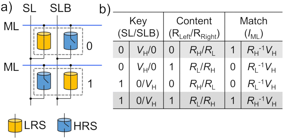 | ||
| Fig. 1 (a) Schematic of the common two resistance-based CAM utilizing passive components. ML, SL, and SLB denote the match line, search line, and complementary search line, respectively. (b) Encoding of a 1-bit key using SL and SLB and 1-bit content using left and right resistors (Rleft and Rright). VH is a pull-up voltage. Matching result is obtained with minimum value of ML current (IML). | ||
However, the common granularity of comparison is rather larger than a single bit, which is a word (a chunk of bits). We conceive the extension of the two switch-based matching mechanisms to 2N complementary switch-based mechanisms in which N LRS and N HRS switches collectively represent a single w-bit word. The advantage is that the combination of 2N complementary switches can represent multi-bit contents while two complementary switches merely single-bit contents. If the entropy of such 2N complementary switches is larger than N bits, the content density exceeds that of N pairs of complementary switches (0.5 bit pert switch). The key requirement is an algorithm for encoding a w-bit word to a 2N-long binary array with N 0s and N 1s. To this end, we utilize the combination-encoding algorithm12 that encodes w-bit words to a 2N-long binary array with N 0s and N 1s, satisfying
| w = ⌊log2C(2N,N)⌋, | (1) |
The CAM based on the combination-encoding of 2N switches (N HRS and N LRS) is referred to as N-CECAM. In this paper, we present an experimental demonstration of this hypothetical CECAM concept of high content density (>0.5 bit per switch) using a passive array of FTJs utilizing Hf–Zr–O (HZO) as a ferroelectric layer. Given the low power consumption of FTJs, FTJ-based CECAM is likely to be a good solution to low-power, high-content-density CAM. To the best of our knowledge, this is the first experimental demonstration of an array of TCAM with a content density exceeding 0.5 bit per switch, which attains 0.75 bit per switch (for 4-CECAM), i.e., a 50% improvement in content density. Furthermore, we designed the layout of CECAM using the SKY130 (130 nm CMOS process) process design kit (PDK)35 to evaluate the cost (additional power and area overheads) of the remarkable increase in content density.
Combination-encoding content-addressable memory based on FTJs
The architecture of FTJ-based N-CECAM (N = 4) is illustrated in Fig. 2. The combination encoder in the figure encodes a w-bit search key kb into a 2N-long binary array with N 0s and N 1s. Note that the subscript b for kb and
  indicates binary representation. The corresponding integer to kb and
  is denoted by k. The encoded key
  is converted to an array of analog voltage signals by a 1-b digital-to-analog converter (DAC). These voltages are applied to the search lines (SLs) simultaneously in the memory domain so that the SLs corresponding to 1s in the encoded key
  are pulled up while the rest of the SLs are maintained at zero. Note that a set of 2N switches (N HRS switches and N LRS switches) in each row represents a combination-encoded content. When the SLs for LRS are grounded while those for HRS are pulled up, the minimal match line (ML) current is detected using a current sense amplifier (CSA), outputting a match signal.
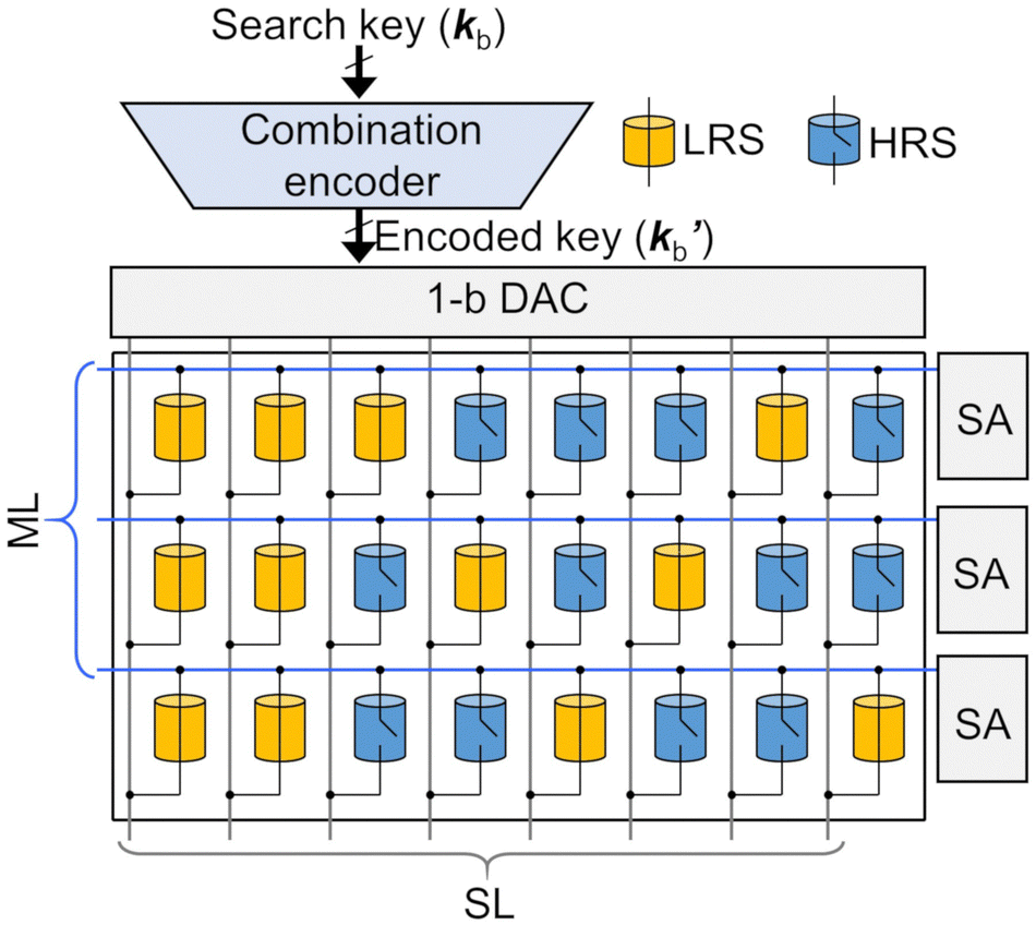 | ||
Fig. 2 Schematic of N-CECAM (N = 4). The search key kb is encoded into a 2N-long binary array  by the combination encoder. Each bit of the encoded key represents the corresponding voltage at search lines (low voltage for 0s and high voltage for 1s). Matching search is obtained at the lowest matching current. by the combination encoder. Each bit of the encoded key represents the corresponding voltage at search lines (low voltage for 0s and high voltage for 1s). Matching search is obtained at the lowest matching current. | ||
Combination encoder
The combination encoder shown in Fig. 2 encodes a w-bit input search key kb to a 2N-long binary array with N 0s and N 1s following the combination-encoding algorithm12 which is elaborated in the following pseudo-code:
function comb_encode(k)
![[thin space (1/6-em)]](https://www.rsc.org/images/entities/char_2009.gif) set
set to 2N-digit binary number 0
fori = 1 toNdo
if there exists c s.t. C(c, N − i) ≤ k < C(c + 1, N − i) then
 [c] ← 1
k ← k − C(c, N − i)
end if
end for
return
end function
The combination encoding is bijective (and thus decodable) for the keys kb of w-bits satisfying eqn (1) as proven in ref. 12. This encoding involves several C(n,r) calculations which need a series of multiplications and divisions. Given that, in C(n,r) calculations required, n is confined in the range 0–2N, and r in the range 0–N-1, we use a N × (2N + 1) lookup table (LUT) P that stores the results of C(n,r) calculations such that P[i,j] = C(j, N − i). Thus, the comparison in the pseudo-code above can readily be performed by searching the LUT P for the value c for a given iteration step i.
A block diagram and data flow for the combination encoder for 4-CECAM are illustrated in Fig. 3 For N = 4, the encoder uses a 4 × 9 LUT P.
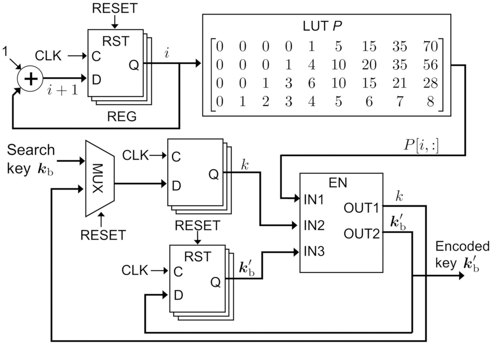 | ||
| Fig. 3 Block diagram of the combination encoder to convert a search key kb to a 2N-long key kb’ with N 0s and N 1s. | ||
Clock and reset signals were utilized to initialize the encoder. The LUT P is used to find 1s in the encoded key  in an iterative manner. Table 1 presents the procedure for encoding a search key kb of integer 111100 (k = 60) in the binary form. After looking for 60 in the first row of LUT, 35 ≤ k = 60 < 75, the eighth position of
  is set to 1, leading to
  = 10000000. The following value of key k, k = 60 – 35 = 25, is applied to the second row of LUT, 20 ≤k = 25 < 35, and the seventh position of
  is set to 1, leading to
  = 11000000. Similarly, the rest of the Bit 1 could be found with k = 25 − 20 = 5,
  = 11001000, k = 5 – 3 = 2, and finally resulting in the encoded key
  = 11001100.
| i | k | Look for k in LUT |
|
|
|---|---|---|---|---|
| 1 | 60 | 35 ≤ k < 70 | 10000000 |
11001100 |
| 2 | 60 − 35 = 25 | 20 ≤ k < 35 | 11000000 |
|
| 3 | 25 − 20 = 5 | 3 ≤ k < 6 | 11001000 |
|
| 4 | 5 − 3 = 2 | 2 ≤ k < 3 | 11001100 |


HZO FTJ crossbar array
FTJ device fabrication
Fig. 4 illustrates the fabrication process flow (Fig. 4a and b) and top view image/transmission electron microscopy (TEM) cross-sectional image (Fig. 4c) of the HZO FTJ crossbar array, respectively. After cleaning the 300-nm-SiO2/Si substrate, a 30-nm-thick Mo was deposited (sputtering) and patterned with reactive ion etching (RIE) as a bottom electrode (BE). A ferroelectric layer (FE)/interlayer (IL) stack of 7-nm-HfXZ1−XrO2 (HZO)/1-nm-ZrO2/2-nm-Al2O3 was deposited with a thermal atomic layer deposition (ALD) at 330 °C. 1 nm ZrO2 was introduced as a second interlayer between the HZO and Al2O3 layers. It has been reported that ZrO2 insertion underneath HZO enhances polarization switching by accelerating the crystallization and increasing the ferroelectric phase of HZO.26 Another 50-nm-thick Mo capping layer was deposited and treated with post-metal annealing at 500 °C in N2 for 30 s utilizing rapid thermal annealing (RTA) to crystalize the HZO layer (annealing for ferroelectricity formation). The top Mo film was patterned (utilizing wet etching instead of RIE to avoid damage near the FE/IL stack) to form the top electrode (TE). Contact holes were formed with RIE in the C2F6 gas before another 50-nm-thick Mo layer was deposited and patterned to form the contact pads. The top view image of the fabricated HZO FTJ array and TEM cross-sectional image of the FTJ stack are presented in Fig. 4c. The FTJs utilized here for CECAM applications were designed to have an area of 10 × 10 μm2.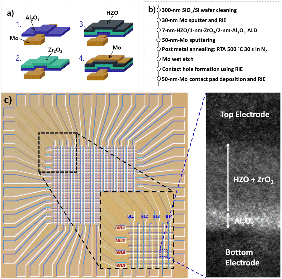 | ||
| Fig. 4 HZO FTJ fabrication illustration (a), fabrication process flow (b) and top view image and cross-sectional transmission electron microscopy (TEM) image of the HZO FTJ crossbar array (c). | ||
The composition of the FTJ stack was characterized by energy dispersive spectroscopy (EDL). The cross-sectional area of the FTJ stack was selected for elemental mapping analysis (Fig. 5). The composition and thickness of each layer were as follows: Mo (Fig. 5a), Al2O3 (Fig. 5b and e), ZrO2 (Fig. 5c and e), and HZO (Fig. 5c–e). The thickness of each layer was determined with the aforementioned distribution of elements.
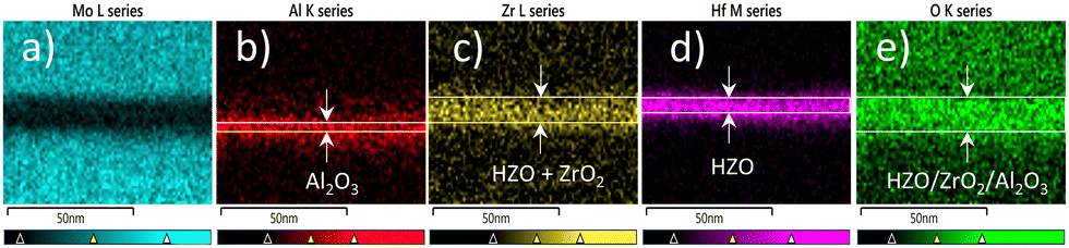 | ||
| Fig. 5 EDS mapping images of FTJ stack utilized in cross-bar array fabrication: elemental maps of Mo (a), Al (b) Zr (c), Hf (d), and O (e). | ||
As depicted in Fig. 6a, the crystallinity of the HZO films was characterized by grazing incidence X-ray diffraction (GIXRD). A high-resolution X-ray diffractometer (X’pert Pro) was used at an incident angle of 0.5°. The GIXRD spectrum of the film (see Fig. 6) indicates that the HZO film is crystallized successfully, with the main peak located near 2θ = 30.5°. Diffraction peaks from the stable monoclinic phase (m-phase, 28.5°) were almost absent, and diffraction peaks from the tetragonal (t-phase) and orthorhombic (o-phase) phases were observed. Because the diffraction peaks at 2θ of 30.6° comprise a mixture of the orthorhombic 111 (111)o and tetragonal 011 (011)t phases, accurate separation of the two phases was challenging. Therefore, approximate ratios were extracted under the assumption that (111)o, (011)t, and (111)m were located at 30.4°, 30.8°, and 31.7°, respectively.36 The ratio occupied by each phase was calculated, and the phase ratios were obtained using the area ratios of the three o-/t-/m-phase peaks. The XRD analysis revealed that the fabricated HZO film had 77% of the o-phase, 17% of the t-phase, and 6% of the m-phase. Confidence coefficients of the o-phase, t-phase, and m-phase fitting results are 98%, 90%, and 65%, respectively.
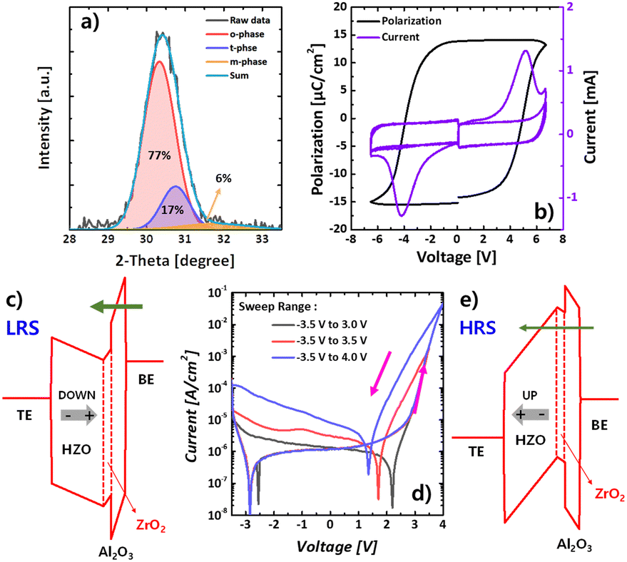 | ||
| Fig. 6 GIXRD spectrum of the 7-nm-thick ferroelectric film: deconvolution peaks and the relative ratio of the o-phase, t-phase, and m-phase in the HZO film (a). Polarization switching current by PUND measurement and the corresponding polarization–voltage (P–V) curve (b) and double sweep IV characteristics with various sweep ranges (d). Energy band diagram for LRS (c) and HRS (e) of FTJ. | ||
HZO FTJ crossbar array performance
The basic electrical characteristics of HZO FTJ are presented in Fig. 6. First, hysteretic tunneling currents were systematically measured to validate the memory properties of the FTJs. The application of direct current (DC) voltage to the TE (VTE) with the grounded BE involved a dual sweep, encompassing both forward and reverse directions. In FTJs with an IL, the electric fields (e-fields) applied to the IL and FE change depending on the polarization states of the FE (energy band diagrams in Fig. 6c and e), thereby modulating the tunneling length for Fowler–Northeim (F–N) tunneling. The tunneling length or tunneling current modulation caused by the change in polarization status is converted directly to a change in resistance, which is defined as tunneling electroresistance (TER). Consequently, at the initiation of forward voltage sweeping, the FE undergoes polarization by −VTE (resulting in a long tunneling length, Fig. 6e), causing the FTJ to exist in a high-resistance state (HRS). Conversely, commencing reverse sweeping with +VTE drives down the polarization (leading to a short tunneling length, Fig. 6c), and the FTJ transitions to a low-resistance state (LRS). The double sweep current–voltage (IV) characteristics in Fig. 6d indicate that no memory window (MW) was detected with a voltage sweep range of 3.0 V. At a sweep voltage of over 3.5 V, the FTJ exhibits clear counterclockwise hysteresis in the +VTE region with the rectified −VTE region, signifying that the MWs are induced by the process of polarization switching.Here, it should be noted that the TER and MW of the fabricated FTJ are determined only by polarization switching. Considering that the resistance of FTJs with an FE and an IL between the two electrodes is determined by the tunneling length, which depends on the stored polarization states in the FE, the continuous increase in TER with increasing applied voltage and abnormally large operation current reported in previous studies are theoretically unexplainable because tunneling dominates the conduction of FTJs (namely, huge tunneling resistance) and the tunneling length can no longer be modulated after the FE becomes completely polarized. This discrepancy was recently explained by a first polarization switching and subsequent resistive switching (by the coexistence of polarization and resistive switching).37 However, the fabricated FTJ has a low operation current, and the second resistive switching cannot be observed (Fig. 6d), indicating that the energy-efficient low-current operation is obtained only by utilizing the polarization switching as a conduction mechanism, indicating that the energy-efficient low-current operation is obtained only by utilizing the polarization switching as a conduction mechanism. Here, it should be noted that the current level can be modulated and increased by controlling the second resistive switching by adjusting the amount and the spatial distribution of the oxygen vacancies inside the ferroelectric layer.38
Positive-up negative-down (PUND) measurements were performed to separate the polarization switching current from the transient and leakage currents.39 In the PUND measurements, polarization switching current was calculated from the difference of positive-up and negative-down as the currents of positive/negative pulse included both switching (ferroelectric switching) and non-switching (displacement and leakage) components and the currents of the up/down pulse had non-switching components only. At a frequency of 105 Hz (a triangular pulse with a rise/fall of 10 μs), the HZO FTJ depicts switching peaks at ±4.2 V (see Fig. 6b) with remnant polarization 2Pr = 28 μC cm−2, which is a typical polarization value of the ferroelectric HZO thin film.39
The switching speed of the HZO FTJ was measured by introducing different program (tP)/erase (tE) pulse widths and program (VP)/erase (VE) voltages before measuring the tunnel current at a DC voltage of 2.3 V (illustrated in Fig. 7a and c). Before each program (erase) measurement, the FTJ was reset by complete erasing (programming). The rise time and fall time of the pulses (for both erase and program) are set at 10 ns in these measurements. The dependences of the tunnel current on the program/erase conditions are illustrated in Fig. 7b and d.
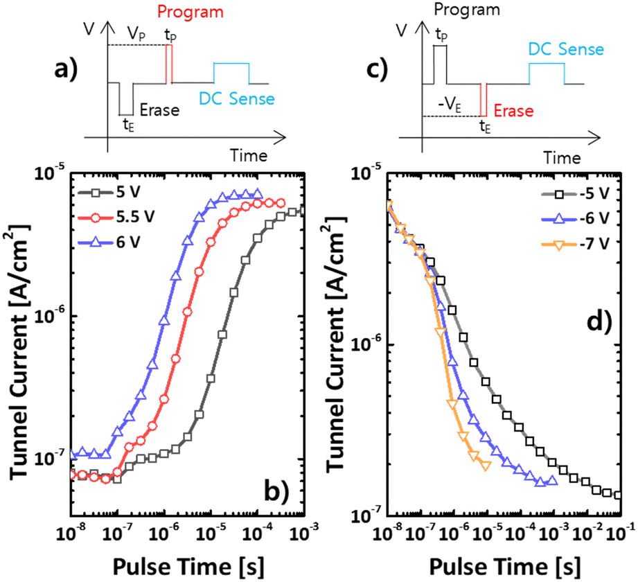 | ||
| Fig. 7 FTJ switching speed characterization: program characterization voltage scheme (a), dependence of tunnel current on program conditions (b), erase characterization voltage scheme (c), and dependence of tunnel current on erase conditions (d). | ||
Endurance and the retention characteristics of the HZO FTJ are summarized in Fig. 8c and d, respectively. Based on the switching properties of the FTJ (Fig. 7b and d), the cycling condition for the stress was determined (triangular pulse with +6/−6 V of peak voltages and a rise/fall time of 10 μs) as depicted in Fig. 8a. The polarization switching current was extracted by the PUND measurement with respect to the number of cycling (Fig. 8b). It is observed that the FTJ woke up within 103 cycles (increasing 2Pr) and then the polarization switching characteristics start to be degraded (reduced 2Pr by fatigue, Fig. 8c). After the cycling stress, the retention properties were monitored at 30 °C as a function of time. Fig. 8d indicates that the LRS and HRS remain stably separated till 104 s although the current difference is slightly reduced by the depolarization of HZO, which guarantees the stable operation of CECAM.
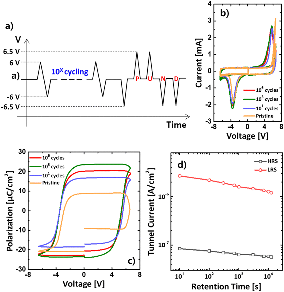 | ||
| Fig. 8 Pulse scheme for stress cycling (a). Changes of polarization switching currents extracted by PUND measurement with respect to the number of cycling (b) and the corresponding P–V curves (c). Retention characteristics measured at 30 °C after cycling (d). | ||
The variability of the HZO FTJ was estimated by analyzing the tunneling currents of the FTJs in the 24 × 24 crossbar array (Fig. 9c). The current values of the HRS/LRS were read at a sense voltage of 2.3 V after applying erase (−6 V)/program (6 V) pulses, respectively. Rise time, fall time, and pulse width of the pulses were set at 100 ns, 100 ns, and 5 μs (target frequency: 105 Hz). For the array operations, the selected cell should be independently operated without disturbing neighbor-inhibited cells. The bias scheme for the inhibition is shown in Fig. 9a where there are three different inhibition cases (inhibit case1, case2, and case3). When a program pulse (VP) is applied to the TE of the selected cell with the grounded BE, half of the VP is simultaneously applied to the unselected TEs and BEs. This inhibition pulse reduces the voltage applied to the unselected cells, effectively preventing their undesirable polarization switching as shown in Fig. 9b where the slight increase of the tunneling current is observed from the unselected cells of inhibit cases 2 and 3. Fig. 9d shows the distribution of tunneling current for the LRS and HRS and the TER ratio distribution (TER ratio was varied from 30 to 70). The TER ratio was calculated by dividing the LRS current by the HRS current. Moreover, the MW distribution (Fig. 9e, where the MW was calculated by the difference of the HRS/LRS voltages extracted at 5 × 10¹¹ A) and the switching window log10(TER) distribution (the contour mapping format of Fig. 9f, where columns and rows indicate the positions of the FTJs in the array) of the FTJ array are plotted, respectively. A uniform FTJ crossbar array was observed. The maximum read power consumption in one switch period (assuming a duty cycle of 99.99%) is Pswitch = ILRS × 2.3 period, which is approximately 5.6 × 10⁻¹⁶ Joule per switch. Therefore, a low power consumption of the CECAM is expected.
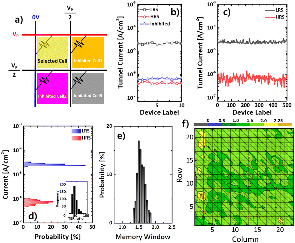 | ||
| Fig. 9 Bias scheme for array operation (a). Tunnelling current changes of unselected cells under inhibit bias conditions (b). HZO FTJ array variability: a tunnel current of 500 FTJs for LRS and HRS (c). Distribution of tunnelling current for LRS and HRS. Inset summarizes the TER ratio histogram of the crossbar array (d). MW distribution (e) and distribution of the switching window, log10(TER) (f). | ||
N-CECAM performance utilizing the HZO crossbar array
The FTJ crossbar array was measured through a 48-pin probe card connected to the switching matrix (E5250A). A Keysight 81110A pattern generator was utilized as the pulse source, and the DC power source was supplied by a semiconductor analyzer 4156B. A visual encoder was created with LabView (a community version of LabVIEW 2020) to convert integer data into binary data such that we could communicate with the FTJ crossbar array through the switching matrix and power sources.Fig. 10a illustrates the performance of a 1-CECAM (or 2 FTJs CECAM) unit or an RCAM unit comprising two HZO FTJs. The integers 0 and 1 also represent “1” and “10” (illustrated in Fig. 1a). The integer of 0 was stored in the 1-CECAM by applying a program pulse (amplitude of 6 V, width of 5 μs, rise/fall time of 10 ns) to FTJ stored Bit “0” while an erase pulse (amplitude of −6 V, width of 5 μs, rise/fall time of 10 ns) was applied to the FTJ stored Bit “1.” Hereinafter, the above conditions of the program pulse and erase pulse were fixed for storing “data” in all CECAM. During searching, Bit “0” and Bit “1” correspond to 0 V and 3 V is applied to the corresponding SL. Fig. 10a summarizes the results of searching 0 (“01”) and 1 (“10”) with the stored data of 0 (“01”). The minimum current at ML matched the stored information.
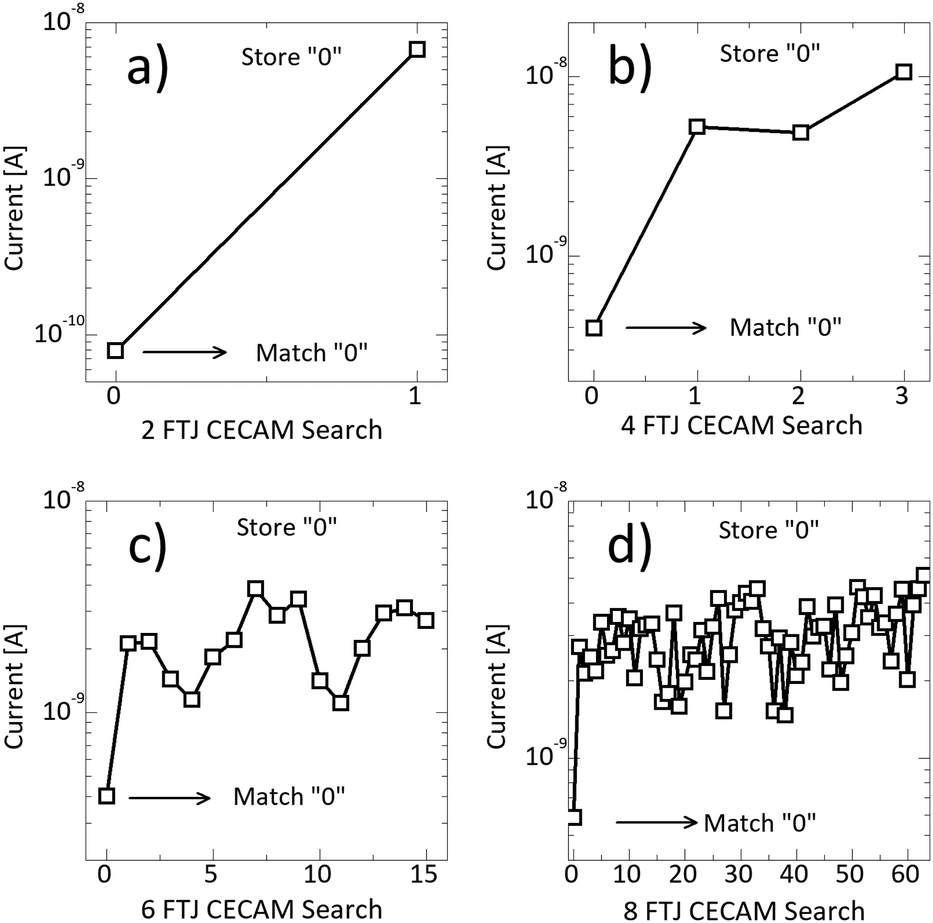 | ||
| Fig. 10 Searching results of N-CECAM based on HZO FTJ (100 × 100 μm2) crossbar arrays with same stored information of “0” with different N values: N = 1 (a), N = 2 (b), N = 3 (c), and N = 4 (d). | ||
Fig. 10b–d summarize the search results (read at ML) in the N-CECAM with N = 2 (four FTJs CECAM), 3 (six FTJs CECAM), and 4 (eight FTJs CECAM), respectively. The integer of 0 represents “01,” “0011,” “000111,” and “00001111” in the CECAM with N = 1, 2, 3, and 4, respectively. All the CECAM indicated that the lowest current was obtained when the search information matched the stored information. With 6 FTJs (switches) and 8 FTJs (switches) in 3-CECAM and 4-CECAM, we created 16 states (4 bits) and 64 states (6 bits), respectively. In other words, the content density of 6-CECAM and 8-CECAM was increased to 0.667 and 0.75 bit per switch instead of 0.5 bit per switch.
The value of the matching current gradually increased with the size of the CECAM (see Fig. 11a), which reduced the mismatch/matching current ratio (Fig. 11b). This comes from the FTJ array variability and the contribution of the leakage current of the FTJs to the search current. Therefore, to further extend the CECAM size, the uniformity of the fabricated FTJs should be improved and the tunneling ratio (LRS/HRS) should be increased simultaneously.
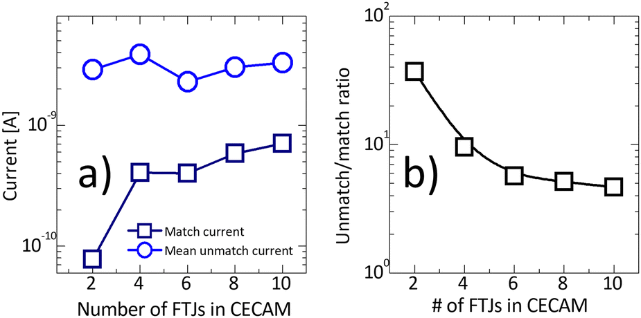 | ||
| Fig. 11 Match current and mean unmatch current at different CECAM sizes (a) and unmatch/match current ratio with the scaling CECAM size (b). | ||
Performance comparison
As such, N-CECAM highlights a higher content density than the conventional 2R-based CAM (Table 2), which likely leads to a higher power efficiency. By simulation, we evaluated the search power consumed by the FTJ array, which was averaged over all 2b search keys and all b-bit contents. These values were normalized to the power consumed by the conventional 2R-based CAM of the same b-bit contents as our N-CECAM. Note that this relative power depends on the HRS/LRS ratio rather than absolute HRS and LRS values. Table 3 lists the relative power for various N-CECAM (1 ≤ N ≤ 6), which highlights the advantage of our CECAM in terms of search power consumption.| Cell type | 2D2R40 | 2PCM41 | 2FTJ42 | 2FTJ27 | 2 Memory diode43 | This work (4-CECAM) |
|---|---|---|---|---|---|---|
| Technology | 28 nm | 22 nm | 180 nm | 28 nm | x | Planar |
| Non-volatility | Yes | Yes | Yes | Yes | Yes | Yes |
| V sense (V) | 1.05 | 1 | 1.6–2 | x | x | 2.3 |
| R HRS/RLRS | ∼100 | ∼20 | ∼100 | ∼100 | ∼1000 | ∼100 |
| Cell area (μm2) | 0.0128 | 0.008 | 0.025 | 0.0461 | 0.01 | 10000 |
| Content density (bit per switch) | 0.5 | 0.5 | 0.5 | 0.5 | 0.5 | 0.75 |
| N | Relative power |
|---|---|
| 1 | 1 |
| 2 | 0.877 |
| 3 | 0.727 |
| 4 | 0.664 |
| 5 | 0.641 |
| 6 | 0.626 |
The high content density of N-CECAM comes at the cost of the additional combination encoder that consumes N logic cycles (cyc_logic) to encode the search keys. These N logic cycles inevitably increase the search latency compared with the conventional CAM with raw search keys. Typically, CAM with CSAs consume three memory cycles (cyc_mem) for a search operation (pre-charging/comparison/sensing);44 the same holds for our CECAM with the encoded search key. Thus, the total search latency for N-CECAM is given by N·cyc_logic + 3cyc_mem while 3cyc_mem for the conventional CAM. Generally, memory cycles are longer than logic cycles (for standard cells) given the sluggish response of memory cells compared with standard cells. For 4-CECAM with 2 ns cyc_logic (500 MHz) and 10 ns cyc_mem (100 MHz), the increase in search latency (due to combination encoding) is approximately 26.7%.
We designed the layout of single bank (128 × 128 FTJs) 4-CECAM using the SKY130 (130 nm CMOS process) open-source PDK35 to estimate the area and power overhead of the peripheral circuits including the combination encoder. The SL decoder addresses eight SLs in parallel, and eight MLs are simultaneously read by using 128 parallel CSAs.
Table 4 identifies that the combination encoder occupies 17.0%, 4.33%, and 6.63% of the total area, power, and energy consumption of the peripheral circuits, respectively.
| Component | Area (μm2) | Power (μW) | Energy (pJ) |
|---|---|---|---|
| Combination encoder | 6715 | 147 | 12 |
| CSA (×128) | 10496 |
1178 | 106.5 |
| SL decoder | 20629 |
2070 | 61.9 |
| Total | 37840 |
3395 | 181 |
Despite these slight increases in area and power overheads, the advantage of CECAM over the conventional CAM is obvious given that the larger content density for CECAM allows larger data to be placed in the 128 × 128 memory array than the conventional CAM.
To measure this advantage, we evaluated the area and power overheads for 4-CECAM (128 × 128) per bit as shown in Table 5. As such, the CECAM (with the additional combination encoder) can significantly improve the area and power efficiencies per content bit thanks to the larger content density.
| 128 × 128 memory array | Area (μm2 b−1) | Power (μW b−1) | Energy (pJ b−1) |
|---|---|---|---|
| CECAM | 3.08 | 0.276 | 0.0147 |
| Conventional | 3.80 | 0.396 | 0.0206 |
Discussion
Although we have experimentally demonstrated the feasibility of FTJ-based CECAM, there still remains daunting challenges to practical implementation in high-density low-latency CAM. They include the low LRS current of our FTJs. For low-latency match-current read using CSAs, the LRS current needs to be on the level of microamps, which is far above the current LRS level. Otherwise, current intergrators can be applied to the match-current read circuit in conjunction with voltage sense amplifiers. However, this causes an additional peripheral circuit overhead and significant read latency. A feasible method to increase the LRS current is to engineer the FTJ stack with a particular focus on the interface between the ferroelectric and electrode layers. The electron tunneling probability is significantly susceptible to the energy barrier profile which largely differs for different cathode materials referred to as the giant electrode effect.45 Thus, the appropriately engineered FTJ stack may achieve its LRS current on the level of microamps. For the moment, we leave this as future work.Conclusion
Content-encoding content-addressable memory utilizing nonvolatile passive memory components (HZO FTJ crossbar array) was successfully fabricated and characterized. By applying a visual encoder, we can communicate with CECAM utilizing the content in the integer-format stored data. The fabricated CECAM exhibits a low match current and searches for the content in a single clock cycle. When the size of the CECAM is increased to more than four FTJs per CECAM unit, the content density increased by higher than 0.5 bit per switch (0.667 and 0.75). This demonstration of CECAM utilizing an FTJ crossbar array facilitates developing more such candidates for reducing the power consumption (nonvolatile memory) and increasing the speed (with a simplified structure) with a higher content density than the conventional SRAM TCAM while retaining the parallel search function of the CAM.Author contributions
M.-C. Nguyen: conceptualization, data curation, formal analysis, investigation, methodology, software, validation, visualization, and writing – original draft. J. W. You: data curation, formal analysis, investigation, methodology, validation, visualization, and writing – original draft. Y. Sim: CECAM circuit design and simulation. R. Choi: funding acquisition, project administration, resources, and supervision. D. S. Jeong: conceptualization, supervision, visualization, and writing – review and editing. D. W. Kwon: funding acquisition, project administration, resources, supervision, visualization, and writing – review and editing.Conflicts of interest
There are no conflicts to declare.Acknowledgements
This research was supported by the Basic Science Research Program through the National Research Foundation of Korea (NRF), funded by the Ministry of Education (No. 2022R1A6A1A03051705). This research was also supported by Korea Basic Science Institute (National research Facilities and Equipment Center) grant funded by the Ministry of Education (2022R1A6C101B762). The EDA tool was supported by the IC Design Education Center (IDEC), Korea.Notes and references
- K. Ni, X. Yin and A. F. Laguna, et al. , Nat. Electron., 2019, 2, 521–529 CrossRef.
- S. Jeloka, N. B. Akesh, D. Sylvester and D. Blaauw, IEEE, J. Solid State Circuits, 2016, 51(4), 1009–1021 Search PubMed.
- I. Arsovski, T. Chandler and A. Sheikholeslami, IEEE, J. Solid State Circuits, 2003, 38(1), 155–158 Search PubMed.
- P. Huang, R. Han and J. Kang, Nat. Electron., 2019, 2, 493–494 CrossRef.
- Y. Zhang, P. Cong, B. Liu, W. Wang and K. Xu, 2021 IEEE/ACM 29th International Symposium on Quality of Service (IWQOS), in Japan, 2021, pp. 1–10 Search PubMed.
- K. Zhou, C. Mu, B. Wen and X. Zhang, et al. , Chip, 2022, 1(2), 100012 CrossRef.
- Y. Kim, et al. , Science, 2018, 360, 998–1003 CrossRef CAS PubMed.
- K. He, Y. Liu, M. Wang, G. Chen, Y. Jiang, J. Yu, C. Wan, D. Qi, M. Xiao, W. R. Leow, H. Yang, M. Antonietti and X. Chen, Adv. Mater., 2020, 32, 1905399 CrossRef CAS PubMed.
- Y. Fu, Y.-T. Chan, Y.-P. Jiang, K.-H. Chang, H.-C. Wu, C.-S. Lai and J.-C. Wang, Adv. Mater., 2022, 34, 2202059 CrossRef CAS PubMed.
- D. Wang, S. Zhao, L. Li, L. Wang, S. Cui, S. Wang, Z. Lou and G. Shen, Adv. Funct. Mater., 2022, 32, 2200241 CrossRef CAS.
- X. Meng, G. Zhang and N. Shi, et al. , Nat. Commun., 2023, 14, 3000 CrossRef CAS PubMed.
- G. Kim, V. Kornijcuk, J. Kim, D. Kim, C. S. Hwang and D. S. Jeong, IEEE Access, 2019, 7, 137620–137628 Search PubMed.
- S. Moradi, N. Qiao, F. Stefanini and G. Indiveri, IEEE Trans. Biomed. Circuits Syst., 2017, 12, 106–122 Search PubMed.
- V. Gaddam, D. Das and S. Jeon, IEEE Trans. Electron Devices, 2019, 67(2), 745–750 Search PubMed.
- S. Jeloka, N. B. Akesh, D. Sylvester and D. Blaauw, IEEE, J. Solid State Circuits, 2016, 51, 1009 Search PubMed.
- I. Arsovski, T. Hebig, D. Dobson and R. Wisort, IEEE J. Solid-State Circuits, 2013, 48, 932–939 Search PubMed.
- K. Niietal et al. , IEEE Int. Solid-State Circuits Conf. (ISSCC) Dig.Tech.Papers, 2014, 240–241.
- C. Gao, et al. , ACM Trans. Rec. Syst, 2023, 1, 1–51 CrossRef.
- B. Max, M. Hoffmann, S. Slesazeck and T. Mikolajick, 48th European Solid-State Device Research Conference (ESSDERC), Dresden, Germany, 2018, 142–145 Search PubMed.
- K.-Y. Hsiang, et al. , IEEE Electron Device Lett., 2021, 42(10), 1464–1467 CAS.
- J. Hwang, Y. Goh and S. Jeon, IEEE Trans. Electron. Devices, 2021, 68(2), 841–845 CAS.
- N. B. Mullani, D. D. Kumbhar, D.-H. Lee, M. J. Kwon, S. Cho, N. Oh, E.-T. Kim, T. D. Dongale, S. Y. Nam and J. H. Park, Adv. Funct. Mater., 2023, 33, 2300343 CrossRef CAS.
- J. Qin, B. Sun, G. Zhou, T. Guo, Y. Chen, C. Ke, S. Mao, X. Chen, J. Shao and Y. Zhao, ACS Mater. Lett., 2023, 5(8), 2197–2215 CrossRef CAS.
- J. H. Sung, J. H. Park, D. S. Jeon, D. Kim, M. J. Yu, A. C. Khot, T. D. Dongale and T. G. Kim, Mater. Des., 2021, 207, 109845 CrossRef CAS.
- G. Dastgeer, S. Nisar, A. Rasheed, K. Akbar, V. D. Chavan, D. K. Kim, S. M. Wabaidur, M. W. Zulfiqar and J. Eom, Nano Energy, 2024, 119, 109106 CrossRef CAS.
- J.-N. Song, M.-J. Oh and C.-B. Yoon, Materials, 2023, 16, 1959 CrossRef CAS PubMed.
- Y. Goh, J. Hwang, M. Kim, M. Jung, S. Lim, S. O. Jung and S. Jeon, IEEE Int. Electron Devices Meeting (IEDM), San Francisco, CA, USA, 2021, pp. 17.2.1–17.2.4 Search PubMed.
- J. Li, R. K. Montoye, M. Ishii and L. Chang, IEEE J. Solid-State Circuits, 2013, 49(4), 896–907 Search PubMed.
- S. Matsunaga, A. Katsumata, M. Natsui, S. Fukami, T. Endoh, H. Ohno and T. Hanyu, Symp. VLSI Circuits-Dig. Tech. Papers, 2011, 298–299.
- E. Garzon, M. Lanuzza, A. Teman and L. Yavits, IEEE Journal on B. Y. Emerging and Selected Topics in Circuits and Systems, 2023, 13, 408–421.
- R. Han, W. Shen, P. Huang, Z. Zhou, L. Liu, X. Liu and J. Kang, Jpn. J. Appl. Phys., 2018, 57(4), 04FE02 CrossRef.
- A. Grossi, E. Vianello, C. Zambelli, P. Royer, J. P. Noel, B. Giraud, L. Perniola, P. Olivo and E. Nowak, IEEE Trans. Very Large Scale Integr. (VLSI) Syst., 2018, 26(12), 2599–2607 Search PubMed.
- C. E. Graves, C. Li, X. Sheng, D. Miller, J. Ignowski, L. Kiyama and J. P. Strachan, Adv. Mater., 2020, 2003437 CrossRef CAS PubMed.
- K. Zhou, et al. , IEEE, J. Solid State Circuits, 2021, 56(3), 988–1000 Search PubMed.
- SKY130 process design kit, online access at https://skywater-pdk.readthedocs.io/en/main/.
- Y. H. Lee, et al. , Nanotechnology, 2017, 28, 305703 CrossRef PubMed.
- W. Shin, et al. , IEEE Electron Device Lett., 2023, 44(2), 345–348 CAS.
- Y. Noguchi, H. Matsuo and Y. Kitanaka, et al. , Sci. Rep., 2019, 9, 4225 CrossRef PubMed.
- J. Müller, T. S. Böscke, D. Bräuhaus, U. Schröder, U. Böttger, J. Sundqvist, P. Kücher, T. Mikolajick and L. Frey, Appl. Phys. Lett., 2011, 99, 112901 CrossRef.
- K. Zhou, et al. , IEEE, J. Solid State Circ., 2021, 56, 988–1000 Search PubMed.
- L. Yang, R. Zhao, Y. Li, H. Tong, Y. Yu and X. Miao, IEEE Electron Device Lett., 2022, 43, 1053–1056 CAS.
- S. Lim et al. , IEEE 48th European Solid State Circuits Conference (ESSCIRC), Italy, 2022, pp. 113–116 Search PubMed.
- X. Wang, Y. Qu, F. Yang, L. Zhao, C. Lee and Y. Zhao, IEEE Trans. Electron Devices, 2022, 69, 259–4264 Search PubMed.
- M. V. Zackriya and H. M. Kittur, IEEE Trans. VLSI Syst., 2017, 25(1), 385–387 Search PubMed.
- R. Soni, A. Petraru, P. Meuffels, O. Vavra, M. Ziegler, S. K. Kim, D. S. Jeong, N. A. Pertsev and H. Kohlstedt, Nat. Commun., 2014, 5414 CrossRef PubMed.
Footnote |
| † The authors contribute equally to this work. |
| This journal is © The Royal Society of Chemistry 2024 |