
 Open Access Article
 This Open Access Article is licensed under a Creative Commons Attribution-Non Commercial 3.0 Unported Licence
High-performance one-dimensional halide perovskite crossbar memristors and synapses for neuromorphic computing†
Sujaya Kumar
Vishwanath
*a,
Benny
Febriansyah
b,
Si En
Ng
 a,
Tisita
Das
c,
Jyotibdha
Acharya
d,
Rohit Abraham
John
a,
Divyam
Sharma
a,
Putu Andhita
Dananjaya
e,
Metikoti
Jagadeeswararao
b,
Naveen
Tiwari
a,
Mohit Ramesh Chandra
Kulkarni
a,
Wen Siang
Lew
e,
Sudip
Chakraborty
*c,
Arindam
Basu
f and
Nripan
Mathews
*ab
a,
Tisita
Das
c,
Jyotibdha
Acharya
d,
Rohit Abraham
John
a,
Divyam
Sharma
a,
Putu Andhita
Dananjaya
e,
Metikoti
Jagadeeswararao
b,
Naveen
Tiwari
a,
Mohit Ramesh Chandra
Kulkarni
a,
Wen Siang
Lew
e,
Sudip
Chakraborty
*c,
Arindam
Basu
f and
Nripan
Mathews
*ab
aSchool of Materials Science & Engineering, Nanyang Technological University, 639798, Singapore. E-mail: sujayav@iisc.ac.in; nripan@ntu.edu.sg
bEnergy Research Institute @ NTU (ERI@N), Nanyang Technological University, 637553, Singapore
cMaterials Theory for Energy Scavenging (MATES) Lab, Harish-Chandra Research Institute(HRI) Allahabad, HBNI, Chhatnag Road, Jhunsi, Prayagraj (Allahabad) 211019, India. E-mail: sudiphys@gmail.com
dSchool of Electrical and Electronic Engineering, Nanyang Technological University, 639798, Singapore
eSchool of Physical and Mathematical Sciences, Nanyang Technological University, Singapore
fDepartment of Electrical Engineering, City University of Hong Kong, Hong Kong
First published on 22nd March 2024
Abstract
Despite impressive demonstrations of memristive behavior with halide perovskites, no clear pathway for material and device design exists for their applications in neuromorphic computing. Present approaches are limited to single element structures, fall behind in terms of switching reliability and scalability, and fail to map out the analog programming window of such devices. Here, we systematically design and evaluate robust pyridinium-templated one-dimensional halide perovskites as crossbar memristive materials for artificial neural networks. We compare two halide perovskite 1D inorganic lattices, namely (propyl)pyridinium and (benzyl)pyridinium lead iodide. The absence of conjugated, electron-rich substituents in PrPyr+ prevents edge-to-face type π-stacking, leading to enhanced electronic isolation of the 1D iodoplumbate chains in (PrPyr)[PbI3], and hence, superior resistive switching performance compared to (BnzPyr)[PbI3]. We report outstanding resistive switching behaviours in (PrPyr)[PbI3] on the largest flexible crossbar implementation (16 × 16) to date - on/off ratio (>105), long term retention (105 s) and high endurance (2000 cycles). Finally, we put forth a universal approach to comprehensively map the analog programming window of halide perovskite memristive devices - a critical prerequisite for weighted synaptic connections in artificial neural networks. This consequently facilitates the demonstration of accurate handwritten digit recognition from the MNIST database based on spike-timing-dependent plasticity of halide perovskite memristive synapses.
New conceptsIn this work, we introduce a pioneering concept in materials science by leveraging pyridinium-templated one-dimensional (1D) halide perovskites as crossbar memristive materials for artificial neural networks. This novel concept distinguishes itself in several crucial ways from existing research. Most notably, we shift the focus from commonly studied three-dimensional (3D) perovskite structures to 1D variants, which exhibit significantly improved resistive switching performance with higher on–off ratios, enhanced endurance, and superior retention characteristics. This emphasis on 1D halide perovskites is a distinguishing feature, as is the innovative design involving (propyl)pyridinium lead iodide, preventing edge-to-face π-stacking interactions and thereby leading to superior performance compared to (benzyl)pyridinium lead iodide perovskites. Furthermore, the scalability of this concept is demonstrated by building the largest known dot-point and crossbar halide perovskite memristive arrays, comprising 50![[thin space (1/6-em)]](https://www.rsc.org/images/entities/char_2009.gif) 000 devices across a substantial area. In addition, our work transcends conventional materials science boundaries and delves into the practical application of these advanced 1D halide perovskite memristors in the domain of neuromorphic computing, exploring spike-timing-dependent plasticity (STDP) learning rules for spiking neural networks (SNN). This multifaceted approach sets our research apart by offering valuable insights into both materials design and real-world computing applications, thereby advancing the field and highlighting the transformative potential of our findings. 000 devices across a substantial area. In addition, our work transcends conventional materials science boundaries and delves into the practical application of these advanced 1D halide perovskite memristors in the domain of neuromorphic computing, exploring spike-timing-dependent plasticity (STDP) learning rules for spiking neural networks (SNN). This multifaceted approach sets our research apart by offering valuable insights into both materials design and real-world computing applications, thereby advancing the field and highlighting the transformative potential of our findings.
|
Introduction
With the increasing computing demands of big data applications, traditional von Neumann hardware architectures are continuously challenged by the need to constantly shuttle data between the separate processor and memory units. This bottleneck becomes critical for data-centric applications like artificial intelligence (AI) and machine learning (ML), and with the near end of Moore's and Dennard's scaling laws, entails new approaches in material, device, architecture and algorithm design to address these novel computing demands.1,2 Characterized by its massively parallel structure interconnecting neurons (computing elements) and synapses (adaptive memory elements), the human brain suggests a non-von Neumann hardware architecture to efficiently handle unstructured data. Inspired by this, neuromorphic electronics – an approach in which devices and circuits mimic the computational elements and signal processing of the human brain, promises to significantly improve the efficiency of artificial neural networks (ANNs) by in-memory computing.3,4 Efficient training and inference of such ANNs rely on the fine modulation of weighted synaptic connections between neuron layers governed by asynchronous spike-based local learning rules such as spike-timing-dependent plasticity (STDP)5 or/and synchronous time-stepped backpropagation algorithms.6Memristor crossbars configured as weighted synaptic connections promise to significantly improve the training and inference of such ANNs in terms of power and speed, compared to conventional graphics processing units (GPUs) for tasks such as image classification and natural language processing.7,8 Although several excellent works have emerged for inorganic memristive devices (mainly metal oxides) by leveraging their nanoscale scalability, stability and reliability,9 many implementations are found wanting with respect to their high energy consumption, unpredictable conductive filaments and diffusion pathways, and unavoidable electroforming processes.10–12 Increasing attention has therefore been given to exploring potential organic materials (e.g. small molecules, polymers, graphene oxide and halide perovskites) due to their unique control of ionic processes, mechanical flexibility, and facile and low cost processability.13,14 Despite the impressive progress already demonstrated in this regard, there are still some intrinsic drawbacks including dissatisfactory environmental stability, irreproducible switching behavior and lack of understanding of the switching mechanisms.15,16 From the neuromorphic circuitry perspective, the switching requirements of memristive devices demand multiple conductance states, non-abrupt switching transitions, wide dynamic range and low write noise.17,18 This differs from the requirements of conventional memory storage technology, where a digital logic with high on–off ratio and switching speeds are given primary importance.19 Most investigations on organic materials and devices limit their analyses to the parameters of a conventional digital logic and fail to map out the analog programming window - essential for ANNs. From a demonstration point of view, investigations on new organic memristive materials and device configurations are often limited to single-element dot-array structures rather than high-density crossbar architectures, again failing to meet the bit precision and storage capacity required for efficient training and inference of ANNs.20,21 Therefore, in order to design new memristive switches as efficient weighted synaptic connections, there is a strong need to explore novel organic active materials, gain insight into the underlying physical mechanism, analyze their switching performance in a crossbar configuration and evaluate their analog programming window.
With an intimately coupled ionic–electronic conduction and a highly tunable compositional landscape, halide perovskites (HPs) possessing exotic optoelectronic properties such as switchable majority carrier concentration, slow photocurrent decay and above bandgap photo-voltages have been very recently evaluated as promising candidates for the next generation of memristive devices.22–26 The co-existence of ionic motion and electronic conduction27 results in a modulatable hysteretic operation, which could be tuned on demand to meet the analog switching requirements of weighted synapses in an ANN.28 Additionally, their facile solution-based low-temperature fabrication would facilitate large-scale realization of dense crossbar arrays at a low-cost.
However, as previously denoted, most of the current HP-based memristive implementations are limited to single-element dot-array structures, and do not sufficiently address the device architecture, scaling and algorithmic aspects, essential to realize large-scale ANNs in hardware. Additionally, most of the investigations rely on three-dimensional (3D) perovskites optimized for photovoltaics and often overlook the more resistive lower dimensional perovskites.29 Specifically from a device configuration perspective, most HP memristors are built with a metal electrode (e.g. Ag) in direct contact with the active perovskite switching matrix. This results in unavoidable metal-HP electrochemical reactions, often limiting the device reliability and endurance.30–32 Also, most devices require a forming step to initiate a stable switching behaviour that results in undesirable power- and time-consuming steps to address the non-volatile states online during training and inference. Finally, from the neuromorphic circuitry perspective, current HP memristor investigations fail to map out the analog programming window of these devices, crucial for ANNs.
In an attempt to solve the above mentioned issues, here we design, fabricate, and systematically evaluate one-dimensional (1D) HP crossbar memristors as weighted synaptic connections for neuromorphic computing. From a materials design perspective, we chose substituted pyridines as templating agents for the formation of 1D structures owing to its relatively high lying LUMO (lowest unoccupied-molecular orbital) relative to the inorganic lattice valence band. This approach helps isolate the 1D chain electronically (i.e. no interaction between the organic and inorganic species). In addition, they are synthetically simple and versatile. We prepare two compositions of 1D HPs with organic cations of different N-substituted functionalities, namely propylpyridinium lead iodide (PrPyr)PbI3 and benzylpyridinium lead iodide (Bnz)PbI3 (Fig. 1). The high band gap of the 1D inorganic lattices and electronic isolation of the inorganic chains enables superior resistive switching performance compared to 3D perovskites – lower off currents, higher on–off ratio between the memresistance states, and ultra-low power read and inference operations. From a device configuration perspective, we adopt an Ag/PMMA/HP/PEDOT:PSS/ITO structure with the active HP switching matrix sandwiched between isolation layers (poly(methyl methacrylate) (PMMA) and poly(3,4-ethylenedioxythiophene):polystyrene sulfonate (PEDOT:PSS)) to avoid the undesirable electrochemical metallization reactions with Ag, thereby improving the reliability, endurance, and retention of the memristive states.
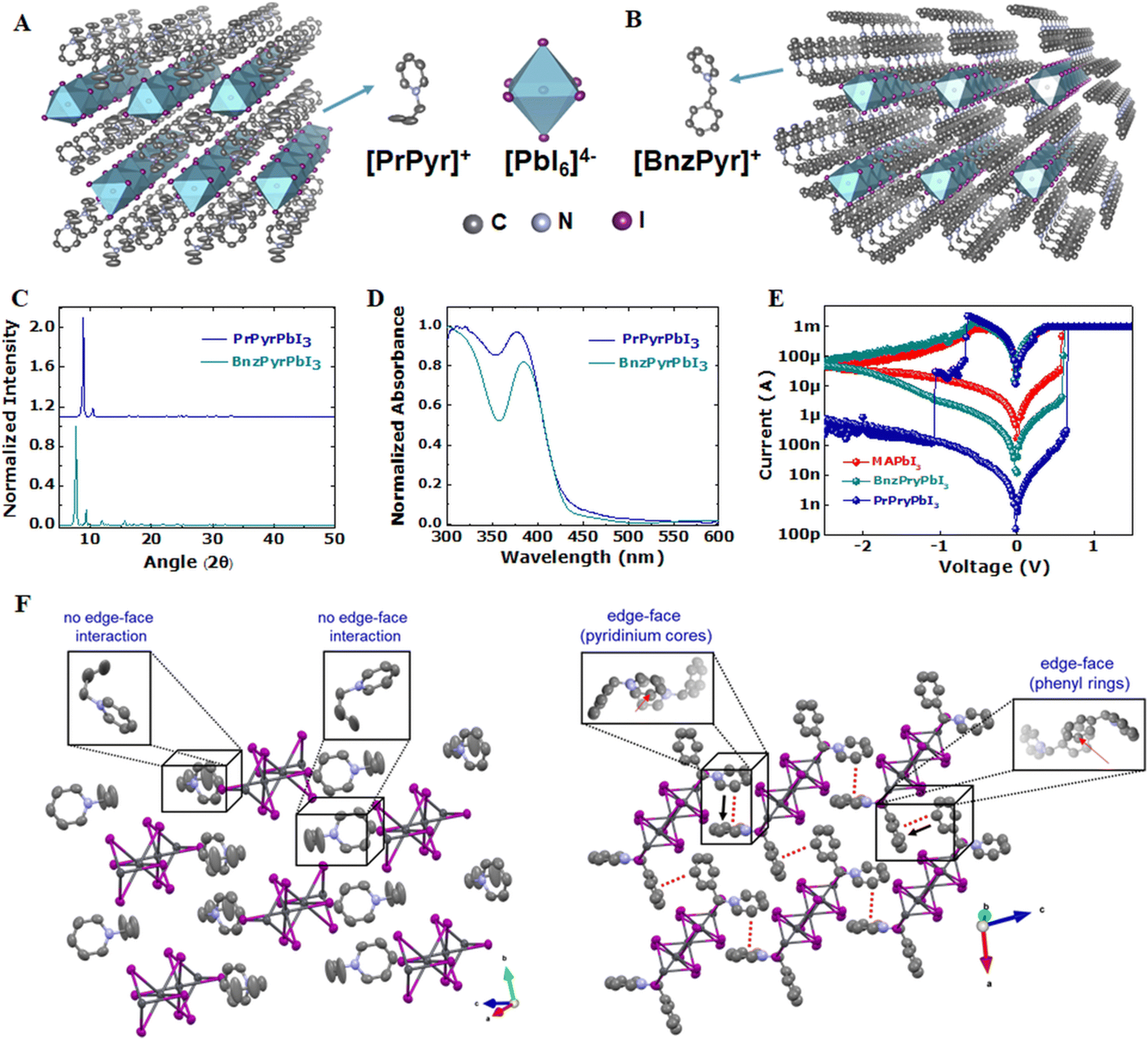 | ||
| Fig. 1 Comparative evaluation of 1D halide perovskites (PrPyr)[PbI3] and (BnzPyr)[PbI3]. Single crystal X-ray structures of 1D lead-iodide hybrids (A) (PrPyr)[PbI3] and (B) (BnzPyr)[PbI3]. Grey, blue, and purple spheroids represent C, N, and I atoms, respectively, while the cyan octahedron represents the [PbI6]−4 coordination sphere. Insets show the molecular structures of PrPyr+ and BnzPyr+ cations. H atoms are omitted for clarity. Thermal ellipsoids are shown at 50% probability. (C) Glancing angle X-ray diffraction (GAXRD) patterns, (D) UV-vis absorption spectra, and (E) I–V characteristics demonstrating the resistive switching effect in three different perovskites, MAPbI3, (PrPyr)[PbI3] and (BnzPyr)[PbI3]. (F) Crystal structure of (BnzPyr)[PbI3] where the edge-to-face type π-stacking interactions of aromatic cores are highlighted with dashed lines within the organic galleries. The square insets show a view down the axis from the perspective of eclipsed aromatic cores (viewing direction is denoted by the black arrows, while the red arrows point to the C atoms containing C–H “H-bond donor” functionalities). | ||
From a process engineering perspective, we follow a facile solution-processable technique and fabricate large-scale dot-array structures (∼50000 elements over 100 cm2) on both rigid and flexible substrates to initially analyse and benchmark conventional device parameters like set and reset, on–off ratio and their distributions across several devices. We extend this further to fabricate the largest flexible HP memristor array to date – a 16 × 16 crossbar architecture (Fig. 2), and rigorously analyse the shelf-life and temperature stability of our devices. Finally, from a neuromorphic computing perspective, to evaluate their fit as weighted synaptic connections in an ANN, we critically identify the digital and analog regimes in the switching characteristics of our devices, i.e. map the analog programming window. We next optimize programming schemes to tap on to the soft boundaries of conductance updates of the devices to study neuronal features such as spike-timing-dependent-plasticity (STDP) (Fig. 3). The applicability of the STDP learning behaviour of 1D HP memristive synapses is further validated through a network level simulation where a spiking neural network (SNN) with HP synapses is trained to classify handwritten digits from the MNIST database (Fig. 4).
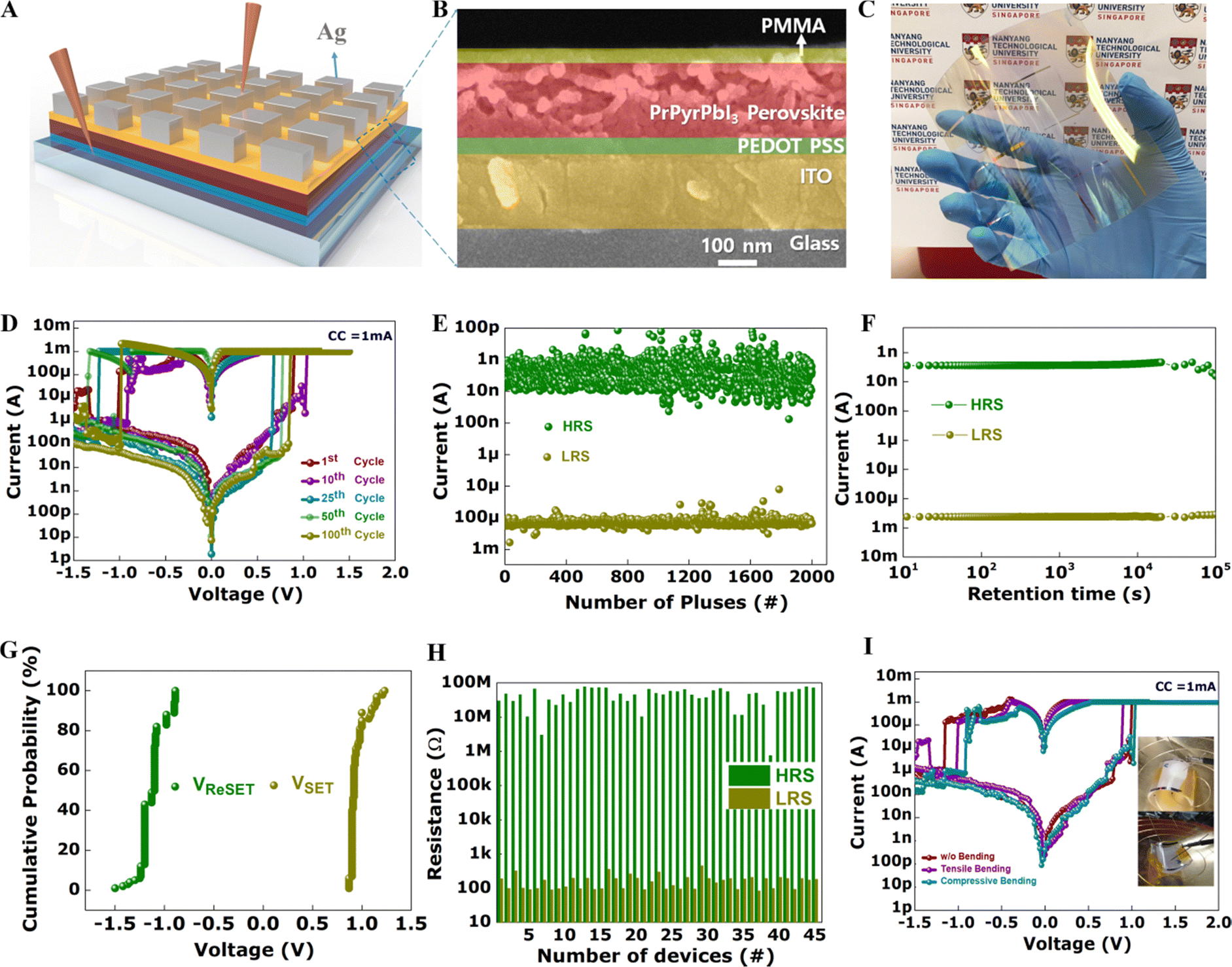 | ||
| Fig. 2 Large-scale flexible PrPyrPbI3 dot-point memristor array. (A) Schematic of the device configuration: Ag/PMMA/PrPyrPbI3/PEDOT:PSS/ITO. (B) Cross-sectional SEM of the fabricated device. (C) Photograph of the large-area dot-point memristor array (∼50000 elements over 100 cm2) fabricated on a flexible PET substrate. Switching characteristics of flexible dot-point memristors: (D) representative DC I–V characteristics demonstrating the resistive switching effect in our devices. The voltage sweeps were applied across the top Ag electrode with the bottom ITO electrode grounded. The devices switched (set) seamlessly from their HRS to LRS at ∼ +0.96 V when the voltage was swept from 0 V → + 1.5 V → 0 V. During set, a compliance current of 1 mA was applied to prevent the device from hard breakdown. On reversing the polarity-0 V → − 1.5 V → 0 V, the device reset back to its initial HRS at ∼−1.21 V. The switching behavior remained consistent over the subsequent 100 sweeping cycles, reflecting the excellent stability of the switching process. Test results of (E) AC endurance and (F) retention. (G) Cumulative probability distribution plot and (H) absolute resistance distribution plot of the LRS (dark yellow) and HRS (olive) across 100 and 45 devices, respectively, and (I) I–V resistive switching characteristics of the flexible HP memristors under extreme bending conditions (tensile and compressive bending radius = 1.5 cm). | ||
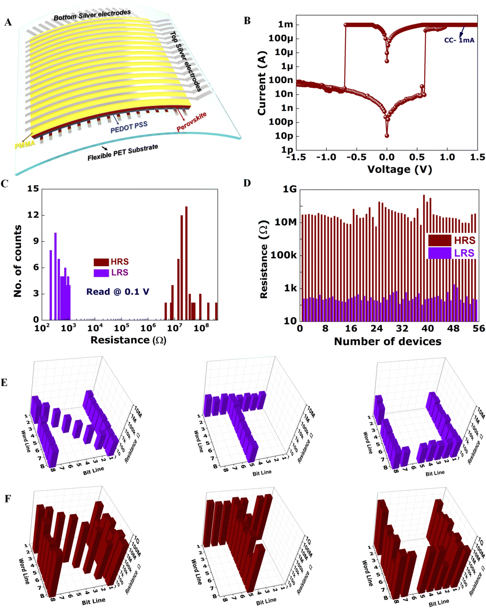 | ||
| Fig. 3 Large-scale flexible PrPyrPbI3 crossbar memristor array. (A) Schematic of the flexible 16 × 16 crossbar memristor array Ag/PMMA/PrPyrPbI3/PEDOT:PSS/Ag-PET. Switching characteristics: (B) representative DC I–V characteristics. (C) Histograms of the resistance values for the memory cells in the LRS (violet) and HRS (purple). (D) LRS and HRS distribution measured across 55 devices. (E) and (F) A basic illustration of the weight modulations that occur across a pixelated array of memristors when employed as synapses in an ANN. The transition from HRS to LRS (set) represents the potentiation phase, while the transition from LRS to HRS (reset) represents depression. To demonstrate the facile reconfigurability of the crossbar array, images of “N”, “T” and “U” were first programmed onto the array using a voltage bias of +1.5 V to set (violet) the pixels corresponding to state-1, while −1.5 V bias was next used to reset (purple) the pixels to state-0. The pixel resistances were read using +0.05 V. | ||
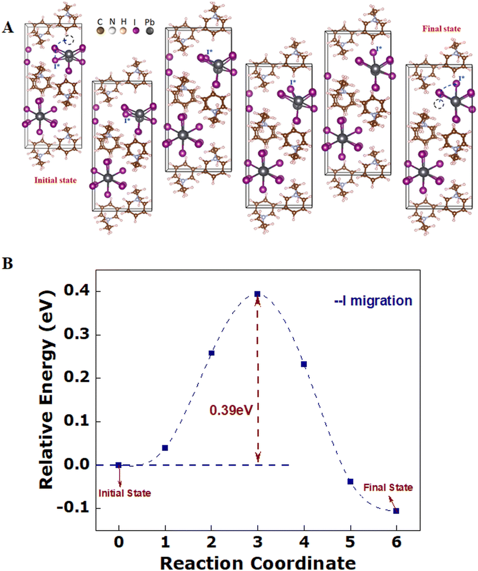 | ||
| Fig. 4 Halide migration in PrPyrPbI3: (A) migration pathway, dotted blue lines show the vacancy migration and black dashed circles represent the vacancies. (B) Energy barrier corresponding to the ion migration barrier. | ||
Results
Fig. 1A and B show the X-ray crystallographic structures of PrPyr[PbI3] and BnzPry[PbI3] along the “a” and “c” axis, respectively. Glancing angle X-ray diffraction (GAXRD) patterns of the thin films of the two 1D-compounds deposited on a glass substrate, depict low angle peaks below 10° – typical characteristics of low dimensional lead-halide materials (Fig. 1C). The crystallites in both compounds tend to strongly orient along the (00l) direction over the substrate, resonating to other 1D hybrid systems such as ethyl viologen lead-iodide.33 Crystallographically, PrPyr[PbI3] and BnzPyr[PbI3] were found to crystallize in the orthorhombic centrosymmetric space group Pnma and monoclinic space group P121/m1, respectively (see SI Note-1 Table T1 for summary of the crystallographic refinement data, ESI†). Due to its relatively bulky structure, PrPyr+ and BnzPyr+ are not capable of inducing a 3D perovskite structure. In addition, albeit being a structural isomer to the commonly used cation phenylethylammonium (PEA), PrPyr+ also does not template the formation of a 2D lead-iodide perovskite network. Instead, both cations induce the formation of anionic polymeric PbI3− chains resulting from the face-sharing [PbI6]−4 octahedra, where each lead (Pb) atom is connected to six iodine (I) atoms, with the octahedral geometry being more or less distorted relative to the ideal lead-iodide octahedron (Note-1 Table T2, ESI†). Despite the potential existence of several C–H⋯I interactions between the inorganic chains and PrPyr countercation, the dominant force for 1D inorganic chain formation appears to be coulombic interactions with the positively charged pyridinium rings. This interaction is directed perpendicular to the plane of the pyridinium rings and causes the cations to align parallel to the inorganic chains. Such an arrangement discourages the formation of a 2D iodoplumbate lattice and is likely the main reason that a structure of lower dimensionality is obtained. We propose that the 1D lead-iodide structure has advantages over the 3D and 2D counterparts due to the enhanced electronic confinement imparted to the inorganic lattice, which leads to the localization of charge carriers in one direction. Such confinement manifests not only in a higher band gap (Fig. 1D, Note-1 Fig. S1, ESI†), but also in sluggish charge carrier transport within the material (i.e. more resistive) and as a result, desirable lower electrical conductivity relative to the HPs of higher dimensionality can be obtained.34,35To confirm the effect of dimensionality on the charge transport properties of the materials in a memristive configuration, we first compared the resistive switching performance of the 1D perovskite compositions BnzPry[PbI3] and PrPry[PbI3] with prototypical 3D MAPbI3 as the control. We first applied our perovskites in the typical configurations employed by previous reports (direct contact with metal electrode); however, they resulted in irreproducible and unfunctional devices varying from batch to batch under our fabrication conditions. Therefore, here we utilized a device configuration with the HP sandwiched between polymeric isolation layers of PMMA and PEDOT:PSS. MAPbI3 exhibited poor resistive switching characteristics with a high off current (5.7 μA) and a low on/off ratio of 102, while BnzPry[PbI3] and PrPry[PbI3] portrayed much higher performances with lower off currents (640 nA and 3.6 nA) and higher on/off ratio of 103 and ∼106 respectively (Fig. 1E). The improved memristive performance of the 1D HP compositions reflects the direct consequence of lowering the electronic dimensionality.
More interestingly, the stark enhancement of the memristive performance of PrPry[PbI3] with respect to BnzPry[PbI3] (Fig. 1E and SI Note-2 Fig. S2–S4, ESI†) points to additional structural aspects that are as significant as the relative energy level positions between the inorganic and organic components within the materials. The observed contrast cannot be attributed to the inorganic lattice framework because the two compounds feature similar structural dimensionality and connectivity. Similar UV-vis absorbance features were also observed from the two compounds, with the main component being the excitonic absorption of the 1D lead-iodide lattices, manifested as intense bands at ca. 375 nm in the spectra (Fig. 1D).36 This suggests that intermolecular charge transfer interaction, which is typically exhibited by compounds containing low-lying LUMO organics, such as viologens or topylium,37,38 is absent in both PrPyr[PbI3] and BnzPyr[PbI3]. Closer examination revealed that the benzyl pyridinium cations in BnzPyr[PbI3] exhibit edge-to-face type π-stacking interactions when viewed down the structure's “a” and “c” axis across the iodoplumbate 1D chains (Fig. 1F). In particular, two edge-to-face type π-stacking interactions were observed – one between the pyridinium cores, and the other between the phenyl rings (see insets of Fig. 1F). This π–π stacking, a significant contributor to the charge transport of small molecules,39–42 is not observed in the crystal structure of PrPyr[PbI3], explaining its superior memristive switching performance. Thus, the difference in conductivity between PrPyr[PbI3] and BnzPyr[PbI3] could be attributed to mobility differences caused by the structural conformations of the aromatic benzyl-based cations that are not seen in the propyl-counterparts. As such, our work demonstrates that the charge transport of 1D perovskite can indeed be tuned as a function of the molecular structure and molecular packing within the organic galleries. To benchmark the properties of our HP memristors with the existing literature, we first fabricate and analyse dot-array structures of Ag/PMMA/PrPyrPbI3/PEDOT:PSS/ITO on rigid glass substrates. A typical dot-point memristor device consists of a ∼200 nm thick PrPyrPbI3 sandwiched between PMMA (20 nm) and PEDOT:PSS (50 nm) layers with Ag (∼100 nm thick, square 100 μm × 100 μm) and ITO (10 Ω □−1) as the top and bottom electrodes, respectively (Fig. 2A). The PrPyrPbI3 films were deposited using a single-step solution-based method as detailed in the Note-1. Fig. 2B shows the cross-sectional scanning electron microscopy (SEM) image of a representative 1D-PrPyrPbI3 memristor, with a compact PrPyrPbI3 layer well sandwiched between PMMA and PEDOT:PSS. From atomic force microscopy (AFM) images, the film surface was found to be smooth (rms roughness ∼7.5 nm (without PMMA) and ∼2.0 nm (with PMMA), SI Note-2 Fig. S2, ESI†) and significantly lower than other reports (typically 50–110 nm),43,44 indicating the high quality of our perovskite films.
Note-2 Fig. S3A (ESI†) shows the resistive switching operation of our devices (0 V → + 1.5 V → 0 V → − 1.5 V → 0 V, step size = 20 mV). All the devices displayed a typical bipolar resistive switching behavior, switching consistently between its high resistance state (HRS) of 2.83 nA and low resistance state of 0.8 mA under a compliance current (CC) of 1 mA for over 50 sweeping cycles, reflecting the excellent stability of the switching process. We next evaluate the endurance, retention, and on–off ratio of the memresistance states to benchmark the switching stability of our devices. A high on–off ratio would ensure a high dynamic range, improved device reliability and signal-to-noise ratio, while excellent endurance and retention properties would ensure stable device operation and easy access of the memresistance states.45,46 Note-2 Fig. S3B–D (ESI†) depicts the endurance, retention characteristics and cumulative probability distribution function of the set and reset voltages of our devices programmed in the window +1.5 V/−1.5 V, respectively. Endurance testing was performed in the alternating current (AC) mode with write voltage pulses applied to the top electrode (Vset 1.2 V/10 ms and Vreset −1.5 V/10 ms), followed by read pulses (Vread = 0.1 V) (Note-2 Fig. S3B, ESI†). A reading voltage of 0.1 V was chosen in order to avoid unintentional switching of the memory devices during the measurements. The devices maintained a high on–off ratio of >105 over both DC sweeping and pulsed AC cycles and exhibited a long retention time of ∼104s (Note-2 Fig. S3C, ESI†), reiterating the stability of the switching process. The average set and reset voltages in our study were +0.9 and −1.0 V respectively, measured over 100 devices with a narrow distribution (Note-2 Fig. S3D, ESI†). This corresponded to average electric fields of 5.6 MV m−1 and −6.25 MV m−1 required for the set and reset processes respectively. The low-voltage operation allows facile programming of the conductance states at ultra-low power, paving the way for power-efficient training and inference of ANNs. In comparison to 3D HP samples prepared parallelly (methylammonium lead iodide (CH3NH3PbI3)), our 1D PrPyrPbI3 HP in general provides a more robust resistive switching behaviour due to the reduced probabilities of ion migration pathways,47,48 enabling higher endurance and retention. In comparison to the lower on–off ratios and unstable switching characteristics depicted by (BnzPyr)[PbI3] (Note-2 Fig. S4, ESI†), (PrPyr)[PbI3] portrays outstanding resistive switching performance. Hence, we focus our efforts realizing crossbar memristors and artificial synapses with (PrPyr)[PbI3] as the active switching matrix as detailed below.
With the emergence of wearable or disposable electronics, there is a growing demand for realizing memory arrays on various flexible substrates. The low temperature processing of our 1D PrPyrPbI3 HP thin film and robustness of its memristive switching characteristics allows us to facilely translate this technology onto a flexible platform (Fig. 2C and Note-3 Fig. S5, ESI†). Harnessing this to our advantage, we fabricate the largest flexible HP memristor array to date to the best of our knowledge (∼50000 elements over 100 cm2) and systematically characterize hundreds of devices. The devices switched seamlessly between its HRS (3.45 nA) and LRS (0.37 mA) in a manner very similar to the devices on rigid substrates without compromising the excellent on–off ratio, retention and endurance, as depicted in Fig. 2D–H. The average set and reset voltages were distributed around mean values of +0.96 V and −1.21 V, respectively, with a narrow distribution measured over 100 devices. Interestingly, our devices display a forming-free operation in contrast to the state-of-the-art reports on HP memristors.49,50 Absence of the forming process helps to overcome undesirable power- and time-consuming steps to address the non-volatile states, thereby increasing the efficiency of the ANNs during training and inference.51 To further highlight the areal uniformity of our process, we characterized multiple devices across randomly selected locations, as shown in Note-3 Fig. S5 (ESI†). The resistive switching behavior was observed to be highly consistent and reproducible preserving an excellent on–off ratio, retention and endurance. In short, the devices depicted excellent and reproducible switching characteristics with an on–off ratio of 105, endurance = 2000 cycles and retention of 105 s. To evaluate the mechanical stability of our flexible memristors, the DC I–V sweeping curves were analyzed in the bent state with a compressive and tensile bending radius of 1.5 cm. The switching characteristics remained robust to mechanical torsion (Fig. 2I). All these features represent a significant advance over previous reports where the switching performance greatly deteriorated on flexible substrates,52,53 highlighting the robustness of our 1D HP memristors. In addition, our perovskite memory devices can switch at a set voltage (1.25 V) with a pulse width of 100 ns (Note-3 Fig. S6 a&b, ESI†) and reset voltage (2.5 V) with a pulse width of 130 ns (Note-3 Fig. S6 c&d, ESI†). We calculated the write energy consumption as follows- Energy consumption/unit area = (1.25 V × 1.1 mA × 100 ns)/104 μm2 yielding an impressive value of 14 fJ μm−2.
As mentioned previously, most of the current HP memristive implementations are based on single-element dot-array structures, ignoring the equally important scaling aspect, which is essential to realize large-scale ANNs in hardware. While the large-area dot point structures presented above establish a significant advance, practical neuromorphic arrays demand dense arrays of memristors in a cross-point configuration capable of accelerating multiply-and-accumulate operations in parallel leveraging Ohm's and Kirchhoff's circuit laws for energy-efficient computations. To address this, we fabricated a 16 × 16 crossbar of HP memristors on a polyethylene terephthalate (PET) substrate, as shown in Fig. 3A. In this configuration, Ag was used as both the top and bottom electrodes, crossing perpendicularly as bit and word lines, respectively. Detailed analyses of the crossbar cells once again indicated excellent forming-free bipolar resistive switching memory characteristics, similar to the dot point structures (Fig. 3B–D and Note-4 Fig. S7, Table T3, ESI†). The histogram plot of the resistance values of the LRS and HRS, reflected well-defined binary states with an excellent on–off ratio of ∼104–106, measured across 55 devices. This again represents a significant advance over the seminal HP crossbar memristor report54 where the switching performance deteriorated on a crossbar configuration, reemphasizing the robustness of our 1D HP memristor. Moreover, the device to device variations were small and the yield of high-performance devices (defined as those with an on–off ratio > 103) was high (90%). Finally, to demonstrate the facile reconfigurability of the crossbar array, images of “N”, “T” and “U” were next programmed onto the array, as shown in Fig. 3E and F. A voltage bias of +1.5 V was used to first set the pixels corresponding to the image “N” to state-1. The pixel resistances were then read using +0.05 V. Next, a −1.5 V bias was used to reset the pixels to state-0. Similarly, new patterns corresponding to “T” and “U” were programmed into the same array after completely erasing the history of “N”. These operations rudimentarily represent the mathematical strengthening and weakening of weighted connections between the neuronal layers in an ANN for image recognition/classification and serves as a preliminary judgement for realizing more complicated architectures in future.
Moreover, the sneak path issue in crossbar arrays without selector55 diodes56 and transistors57 can be a significant challenge. Sneak paths occur when unselected devices that share one electrode with the selected device experience half of the bias, leading to unintended current flow and potential errors in the array operation. It is acknowledged that our perovskite crossbar would benefit from the incorporation of a selector device 55. Monolithically integrating a selector on top of the crossbar presents challenges, but in future, a bottom-up approach for integration could be feasible due to the low-temperature processing of perovskite crossbar devices.
Furthermore, in order to understand the experimental observations of outstanding resistive switching behaviours for neuromorphic computing, we have performed electronic structure calculations of 1D iodoplumbate chains in (PrPyr)[PbI3], within the framework of the density functional theory (DFT) formalism to determine the halide ion migration, while comparing it with the conventional 3D hybrid perovskite MAPbI3.
In order to find the iodine migration, we have performed a series of systematic transition pathway calculations based on the nudged elastic band (NEB) formalism. For such transition pathway prediction corresponding to iodine migration, we have considered a number of possible energy configurations having different initial and final points, while Fig. 4a depicts the ion migration corresponding to the minimum most energy configuration, which consists of five intermediate images between the initial and final points in (PrPyr)[PbI3]. The energy barrier corresponding to the ion migration barrier in the PrPyrPbI3 perovskite system is 0.39 eV, as shown in Fig. 4b. Our theoretical finding of the activation energy barrier is in good agreement with the experimental observation, as we found that the activation energy for iodine migration is larger than that in MAPbI3 having a barrier of 0.29 eV in the earlier reports.58,59 There is another report on the ion migration in 3D MAPbI3, performing similar DFT calculations like ours, which demonstrates the value as 0.16 eV.57 Considering both the reported results, our halide migration has emerged as slower with a higher activation energy barrier. These reduced probabilities of ion migration pathways in PrPyrPbI3 as compared to 3D MAPbI3 suggest better performance in any memristor device with improved resistive switching performance having higher on–off ratio, endurance and retention characteristics as found in experimental observations.
To effectively develop software algorithms to run memristive ANNs, it is necessary to map the window of analog programmability and understand the conductance update under different programming conditions. Bound conductance values and state-dependent modulation are key factors influencing the neural network's storage capacity and efficiency, but are often overlooked. As a final evaluation of the switching requirements of weighted connections in an ANN (Fig. 5A), we analyze the analog programming window of PrPyrPbI3 memristors. Ideally, to account for the large number of weight update operations in an ANN training algorithm like backpropagation, memristors deployed as synaptic connections between neuron layers must be able to store multiple bits of information across continuously distributed conductance states with non-abrupt/analog state transitions. However, most memristive implementations depict a binary switching logic, limiting their plasticity and storage capacity, and adversely affecting the trainability of an ANN. Although our HP memristors also depict a binary logic and abrupt switching transitions in the DC sweeping cycles, the close coupling between ionic motion and electronic conduction allows for intermediate resistance states to form, allowing a higher margin to access intermediate resistance states in the pulsed/AC mode and enabling good control over the digital and analog switching regimes. Hence utilizing pulsed voltage schemes, we first map the soft boundaries for weight updates, a.k.a. analog programming window, in our devices.
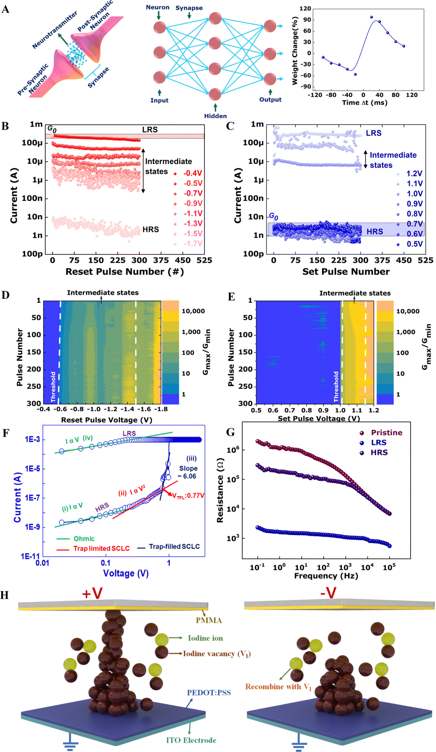 | ||
| Fig. 5 Evaluating (PrPyr)[PbI3] memristors as weighted synaptic connections in an ANN. (A) Schematic illustrating the analogy between a biological and an artificial neural network, highlighting the synaptic junctions between neurons. The image on the right depicts the asymmetric Hebbian STDP rule implemented in (PrPyr)[PbI3] synapses. Mapping of the analog programming window. Plot of the conductance updates with uniform (B) reset and (C) set pulses. State-dependent modulation – the conductance window Gmax/Gmin with respect to the number and amplitude of the (D) reset and (E) set pulses. Analysis of the switching mechanism. (F) logI–logV characteristics of the (PrPyr)[PbI3] memristor depicting the 3 regions of conduction-ohmic, trap-limited and trap-filled SCLC. (G) Electrochemical impedance spectroscopy with Bode plot comparison of the resistance at various resistance states, and (H) graphical illustration of the switching mechanism during the set and reset processes. | ||
To evaluate the soft bounded nature of the cumulative conductance change, i.e., to map the voltage window where PrPyrPbI3 would allow non-abrupt synaptic update operations, absolute weights were programmed to a common initial conductance and weight traces produced by sequences of 300 identical pulses were recorded as a function of the number of pulses. Input pulses of amplitude +0.5 V to +1.2 V were used to map the weight updates during potentiation, while −0.4 V to −1.7 V mapped the depression window. The weight update traces evolved from a region of no substantial conductance/weight change to regions of gradual/analog and then to the abrupt/digital switching regime (from dark to clear color tones), as illustrated in Fig. 5B and C. The regions of no, analog and digital switching were distinguished based on the definition of on–off ratio as <1, 1–100 and >100, respectively. Based on these definitions, the analog programming windows of potentiation and depression were estimated to be between +1.0 to +1.2 V and −0.4 to −1.5 V respectively. Input voltages below this window did not produce any stable non-volatile conductance change, while voltages above this window resulted in abrupt/digital switching, reflecting the limited window for truly analog weight updates (Note-5 SI Fig. S8, ESI†), ideal for ANNs.
Plots of conductance ratios (Gmax/Gmin) as a function of the pulse programming parameters (amplitude and number of repetitions) exposed further insights into the analog programming window (Fig. 5D and E). The first vertical dashed line represents the switching threshold for non-volatile changes, while the second dashed line demarcates the soft boundary for analog weight updates. This window denotes the operational region where weight changes are incremental and non-abrupt, ideal for ANNs. The voltage–time (pulse number) relation revealed a steeper slope in the potentiation phase, indicating more abrupt switching kinetics of the potentiation process when compared to depression. This reflected the difference in switching kinetics for potentiation and depression, and indicated a larger window of analog programmability for depression when compared to potentiation. This suggests a state-dependent weight updatability modulation in such memristive devices, often overlooked in most investigations, and provides a sound guideline to tap onto this region from an algorithm perspective.
After mapping our memristor's soft boundaries of analog programmability, we next benchmark our systems against the most widely used plasticity law in spiking neural networks, namely spike-timing-dependent-plasticity (STDP). Long-term plasticity refers to the brain's ability to restructure its connections. Analogously, ANNs determine their connection strength using gradient descent during training, calculated via backpropagation, which could be compared to contrastive Hebbian long-term plasticity.60 Here, the 2 sub-components of long-term plasticity, namely potentiation (LTP) and depression (LTD), were first studied by applying consecutive pre-synaptic training pulses (+1 V for LTP and −1 V for LTD, pulse width = 10 ms) at the top electrode. Weight changes were studied as a function of the number of pulses as shown in Note-6 Fig. S12A (ESI†) and were observed to follow a non-linear model in agreement with Fig. 5B and C. While these represent the mathematical weight update operations, temporal correlations in spiking neural networks are often embedded into the system via STDP rules.61 A refinement of Hebb's theory, STDP is regarded as the first law of synaptic plasticity, forms the foundation of associative learning and is a figure-of-merit of plasticity for unsupervised learning.62 To characterize this plasticity rule, spike patterns corresponding to Note-6 Fig. S12B (ESI†) were applied to the pre- and post-synaptic terminals as indicated, and the change in conductance (weight) was recorded as a function of the pulse interval between pre- and postsynaptic spikes as detailed in the ESI.† Temporal correlations between the pre- and postsynaptic spikes created voltage-dependent changes in conductance/weight, establishing an asymmetric Hebbian STDP rule (Fig. 5A) as detailed in Note-5 (ESI†).
Formation of conductive filaments via electrochemical metallization reactions and valence change mechanisms due to the anion vacancies are often identified as the underlying principles for resistive switching in HP memristors.63 While the former dominates in configurations where an active metal like Ag or Cu is in direct contact with the HP, the latter is observed in most configurations due to the low activation energy for ion migration. Nevertheless, most current implementations use a reactive metal electrode (e.g. Ag/Al/Cu) in direct contact with the active perovskite switching matrix, leading to unavoidable metal-HP electrochemical reactions, often limiting the device reliability and endurance.64–66 More critically, this leads to multiple competing resistive switching phenomena existing in the same device, namely electrochemical metallization (conductive filament formation via metal-HP reaction) and valence change mechanisms (widely attributed to migration of halide vacancies), resulting in unreliable and irreproducible switching transitions, detrimental to the training and inference of ANNs. Such deleterious metal-HP electrochemical reactions, even with inert metals like gold, have been widely observed and critically judged in the perovskite photovoltaic community using various spectroscopic and microscopic investigations. The sandwich device configuration we adopt, Ag/PMMA/HP/PEDOT:PSS/ITO with the PMMA and PEDOT:PSS layers protecting the active HP, enables us to eliminate such undesirable electrochemical reactions. To account for the memristive behaviour in our devices, we analyse the logarithmic I–V characteristics as a first judgement of the underlying switching mechanism, as shown in Fig. 5F. As shown, the HRS and LRS depicted different behaviours, corresponding to space-charge-limited conduction (SCLC) and ohmic conduction, respectively. Before the set process, the SCLC model in HRS indicated two regions, an initial ohmic region (where the slope (S) of the I–V plot yielded a value of 1, i.e. IαV) and a region obeying Child's law (IαV2). On the other hand, the LRS was consistently governed by an ohmic behaviour after the set process.67 In order to further understand the interface and charge transport various resistance states, impedance spectroscopy was carried out. While a conventional DC I–V sweep can only give steady-state properties including bulk resistance and resistive switching voltage, an alternating current (AC) measurement can provide a transient response, such as impedance and capacitance. By analyzing the frequency-dependent transient response attributed to ionic–electronic conduction in the perovskite film, we can interpret the charge transport at the microscopic scale (nature of charges and interface/bulk properties). Here, impedance spectroscopy utilizes an alternating perturbation signal of 40 mV to probe the temporal response of the system, and the current response is recorded at various frequencies of 0.1 to 100 kHz.
The frequency-dependence can be clearly seen in Fig. 5G and Note-5 Fig. S9 (ESI†), and both the HRS and the pristine state show lower resistances at high frequency, suggesting a mixed conduction of both electrons and ions across the bulk film. However, at lower frequency, the resistance increases with the accumulation of sluggish ions at the electrodes; the interfacial polarization also results in a higher capacitance measured (Note-5 SI5-Fig. S9a and b, ESI†). At high frequency, the capacitance approaches ∼0.5 nF, which is approximately the geometrical capacitance of the device. When the device is SET to the low resistance state, the device exhibits monotonous frequency dependence resembling electronic conduction in a conductive filamentary path. (ESI†).68,69 The impedance spectrum did not exhibit any negative capacitance arc or the chemical inductance arc, supporting the filamentary formation hypothesis.70
To further probe the underlying mechanism, we performed retention failure analysis of the LRS as a function of temperature, as shown in Note-5 Fig. S10a (ESI†). Widely accepted in the oxide memristor research community as a cause for retention failure at the LRS, this model accounts for the migration and redistribution of ions and vacancies and also takes into account spontaneous diffusion via concentration gradients.71 Specifically, the diffusion process is fit to a thermally-activated model and the retention time (t) is observed to be proportional to exp(Ea/kT), where Ea is the activation energy for ion migration, k is the Boltzmann constant, and T is the absolute temperature. Following this method, measurements of temperature-dependent retention were performed to establish the diffusion energy barrier for the species that induces switching in our PrPyrPbI3 film. Note-5 Fig. S10a (ESI†) shows the retention measurement results of Ag/PMMA/PrPyrPbI3/PEDOT:PSS/ITO devices at LRS (≈383 Ω) at different temperatures. A small constant read bias (0.1 V) was applied to monitor the evolution of resistance over time. The retention time decreased from 1200 to 60 s when the temperature was raised from 363 to 400 K. The activation energy for ion migration (Ea) was derived to be equal to 0.18 eV from the linear relationship between ln(t) versus 1/kT (Note-5 Fig. S10b, ESI†). This is consistent with the values recorded for I− ions (0.1–0.6 eV), hence suggesting the movement of I− ions to be the dominant process that causes memristive switching in our devices.72,73
Therefore, we attribute the switching mechanism predominantly to the conductive filament formation due to the migration of anion vacancies within the HP layer. We hypothesize that upon application of a positive set voltage at the top electrode, positively charged iodide vacancies drift towards the bottom electrode, forming highly conductive filaments shorting the device to its LRS. On reversing the polarity, these vacancies get partially filled, rupturing the conductive filaments and bringing the device back to it HRS (Fig. 5H). Furthermore, we replaced the silver (Ag) top electrode with electrochemically inert gold (Au) in the device fabrication. The resulting Au/PMMA/PrPryPbI3/PEDOT:PSS/ITO/PET devices exhibited similar resistive switching characteristics (RS) with an on/off ratio exceeding 105, as illustrated in Note-5 Fig. S11 (ESI†). However, self p- and n-doping of the HP bulk during this ion drift-diffusion process, modulation of the injection barrier at the HP-PEDOT:PSS interface and doping of the injection layer itself could also contribute to the resistive switching process.28 Moreover, all the constituent ions except probably the bulky PrPyr+ cation, namely I− and Pb2+, and defects such as vacancies, interstitials, and anti-sites have low activation energies for migration74 and could contribute to the resistive switching, making it difficult to diagnose the exact switching mechanism. With respect to long-term plasticity rules like LTP, LTD and STDP, persistent training with voltage pulses results in more vacancies/ions being accumulated to form/disrupt conductive filaments through the bulk or perturb the injection barriers at the interfaces, hence increasing/decreasing the conductance permanently similar to the set/reset processes in conventional memristors. The short intervals maintained between such training pulses do not allow the vacancies/ions to relax or diffuse back to their original positions, resulting in precise conductance modulations.
Exploiting the STDP property of the PrPyrPbI3 synapse, we simulated a spiking neural network (SNN) for a handwritten digit recognition task.75 The network is trained and tested on images of handwritten digits from the MNIST database.76 The input images are first converted to Poisson spike trains and fed to the excitatory neurons through HP synapses. Each excitatory neuron is connected to one inhibitory neuron and each inhibitory neuron is connected to all other excitatory neurons. The HP synapses from input to excitatory neurons are initialized with random weights and then, learned through STDP. The connections between excitatory and inhibitory neurons are static (fixed weight). Whenever an excitatory neuron spikes, the corresponding inhibitory neuron also spikes and through one to all inhibitory connections, it ensures that no other excitatory neuron spikes. Therefore, through this lateral inhibition, a winner-takes-all strategy77,78 is implemented. The architecture of the network is shown in Fig. 6A. In our first simulation, we trained the network on 6000 training images and evaluated the performance on 1000 testing images. All experiments were done with varying numbers of neurons. The network reaches an accuracy of 79.8% for 400 neurons (Fig. 6B).
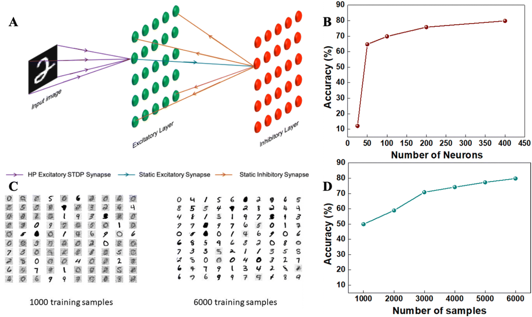 | ||
| Fig. 6 STDP learning for unsupervised digit recognition using HP synapses. (A) Architecture of the SNN trained for a handwritten digit recognition task. The input image is converted to Poisson spike trains and fed to excitatory neurons through STDP synapses. A winner-takes-all strategy is implemented through lateral inhibition by inhibitory neurons in the second layer. (B) Accuracy is plotted for a varying number of input neurons with 6000 training and 1000 testing samples taken from the MNIST handwritten digits dataset. 79.8% accuracy is obtained for 400 neurons. (C) Receptive fields of 100 neurons are visualized after 1000 and 6000 training samples, respectively. Receptive fields show better and more diverse representations of input patterns with an increasing number of training samples. (D) Classification accuracy for varying numbers of training samples reaching ∼80% for 6000 samples. | ||
Now, during the training of the SNN, whenever an excitatory neuron spikes in response to a specific input pattern, the receptive field of that neuron becomes more attuned to that input pattern through STDP learning. In Fig. 6C, the receptive fields of 100 neurons are shown after training the network with 1000 and 6000 samples, respectively. As we can see from the figure, not only do the receptive fields more accurately resemble the input patterns, but also we get a larger number of representations for the same digit with increasing number of training samples. Finally, we plot the classification accuracy of the network with varying number of training samples (Fig. 6D). The steady increase in accuracy with increasing number of training samples is in accordance with the observations from Fig. 6C. Further details of the simulation are described in SI-Note 6. To verify the validity of the proposed simulation when device-to-device (16 devices) variations of STDP parameters are included, around 1.2–1.6% loss of accuracy was found (SI-Note 6 Fig. S13 &14, ESI†).
Conclusion
To conclude, here we design, fabricate and systematically evaluate pyridine-templated 1D halide perovskite (HP) materials as crossbar memristors and weighted synaptic connections for artificial neural networks. In comparison to 3D perovskites (e.g. MAPbI3)), the 1D HPs portray an improved resistive switching performance with higher on–off ratio, endurance and retention characteristics due to the reduced probabilities of the ion migration pathways,79,80 higher band gap of the 1D inorganic lattices and electronic isolation of the inorganic chains. By designing organic galleries without π-stacking interactions, we demonstrate PrPry[PbI3] memristive materials in both dot-point and crossbar configurations with outstanding resistive switching performance when compared to BnzPry[PbI3] perovskites that possess structural conformations of the aromatic benzyl-based cations. The benchmarking parameters extracted from the PrPyrPbI3 memristors, such as low off currents (∼nA), on–off ratio (∼106), retention (105 s) and endurance (2000 cycles). The resistive switching mechanism is attributed to the migration of vacancies/ions in the HP, self-modulating the bulk and interfaces of the memristive device structure. We build the largest dot point and crossbar HP memristive arrays to date (50000 devices across an area of 100 cm2 and 16 × 16 crossbar) and methodically characterize 100 s of devices. We report the first comprehensive analysis of the analog programming window for organic memristive materials, specifically halide perovskites, and investigate spike-timing-dependent plasticity (STDP) learning rules for spiking neural networks (SNN). This soft-boundary estimation can be extended to all memristive platforms and provides a comprehensive guideline for analog programming of weighted synaptic connections. Furthermore, the STDP learning of the synapses is substantiated though an SNN simulation with HP synapses that achieves 79.8% classification accuracy on a handwritten digit recognition task for 6000 training and 1000 testing samples from the MNIST database. In summary, the family of HP semiconductors offers a highly malleable material platform for developing novel memristive devices and artificial synapses, exploiting their unique ionic–electronic conduction. Our findings motivate further exploration of the dimensional and compositional space of HPs, to investigate the correlation between material properties and memristive behavior. This paves the way for new ionic–electronic neuromorphic architectures with halide perovskites as the active material.
Experimental section
Please refer to the ESI† for details on the experimental procedure, device fabrication and characterization.Conflicts of interest
There are no conflicts to declare.Acknowledgements
This research was funded by the Ministry of Education, Singapore Tier 2 Grant-MOE2018-T2-2-083 and National Research Foundation, Prime Minister's Office, Singapore under its Competitive Research Programme (CRP Award No. NRF-CRP14-2014-03). T. D. and S. C. would like to acknowledge HRI Allahabad and DST-SERB Funding (SRG/2020/001707) for the infrastructure and funding. Computational work for this study was carried out at the cluster computing facility at Harish-Chandra Research Institute (https://www.hri.res.in/cluster). S. K. V., R. A. J., and N. M. conceived the project and experimental flow. S. K. V., B. F. and D. S. fabricated the crossbar memristor devices and characterized the non-volatile memory properties. M. J. performed the cross-sectional SEM experiments. T. D. performed DFT computational work under the supervision of S. C. N. T. took the AFM images. S. K. V., S. N. and P. A. D. carried out the neuromorphic characterizations. J. A performed the spiking neural network simulations under supervision of A. B. S. K. V., B. F., R. A. J., J. A, A. B and N. M. wrote the manuscript with input from all the authors.References
- E. Nature, Nature, 2018, 554, 145–146 Search PubMed.
- M. A. Zidan, J. P. Strachan and W. D. Lu, Nat. Electron., 2018, 1, 22 CrossRef.
- K. Roy, A. Jaiswal and P. Panda, Nature, 2019, 575, 607–617 CrossRef CAS PubMed.
- Y. van De Burgt, A. Melianas, S. T. Keene, G. Malliaras and A. Salleo, Nat. Electron., 2018, 1, 386–397 CrossRef.
- P. U. Diehl and M. Cook, Frontiers in computational neuroscience Search PubMed.
- M. Courbariaux, Y. Bengio and J.-P. David, Advances in neural information processing systems, 2015, pp. 3123–3131 Search PubMed.
- G. W. Burr, R. M. Shelby, A. Sebastian, S. Kim, S. Kim, S. Sidler, K. Virwani, M. Ishii, P. Narayanan and A. Fumarola, Adv. Phys. X, 2017, 2, 89–124 Search PubMed.
- A. Sebastian, M. Le Gallo, R. Khaddam-Aljameh and E. Eleftheriou, Nat. Nanotechnol., 2020, 1–16 Search PubMed.
- M. Prezioso, F. Merrikh-Bayat, B. D. Hoskins, G. C. Adam, K. K. Likharev and D. B. Strukov, Nature, 2015, 521, 61–64 CrossRef CAS PubMed.
- J. S. Lee, S. Lee and T. W. Noh, Appl. Phys. Rev., 2015, 2, 31303 Search PubMed.
- J. Y. Seok, S. J. Song, J. H. Yoon, K. J. Yoon, T. H. Park, D. E. Kwon, H. Lim, G. H. Kim, D. S. Jeong and C. S. Hwang, Adv. Funct. Mater., 2014, 24, 5316–5339 CrossRef CAS.
- C. S. Hwang, Adv. Electron. Mater., 2015, 1, 1400056 CrossRef.
- Z. Y. Wang, L. Y. Wang, M. Nagai, L. H. Xie, M. D. Yi and W. Huang, Adv. Electron. Mater., 2017, 3(7), 1600510 CrossRef.
- J. Tang, F. Yuan, X. Shen, Z. Wang, M. Rao, Y. He, Y. Sun, X. Li, W. Zhang, Y. Li, B. Gao, H. Qian, G. Bi, S. Song, J. J. Yang and H. Wu, Adv. Mater., 2019, 31(49), 1902761 CrossRef CAS PubMed.
- H.-L. Park, Y. Lee, N. Kim, D.-G. Seo, G.-T. Go and T.-W. Lee, Adv. Mater., 2020, 32, 1903558 CrossRef CAS PubMed.
- J. Tang, F. Yuan, X. Shen, Z. Wang, M. Rao, Y. He, Y. Sun, X. Li, W. Zhang, Y. Li, B. Gao, H. Qian, G. Bi, S. Song, J. J. Yang and H. Wu, Adv. Mater., 2019, 31(49), 1902761 CrossRef CAS PubMed.
- Y. van de Burgt, E. Lubberman, E. J. Fuller, S. T. Keene, G. C. Faria, S. Agarwal, M. J. Marinella, A. A. Talin and A. Salleo, Nat. Mater., 2017, 16, 414–418 CrossRef CAS PubMed.
- E. J. Fuller, S. T. Keene, A. Melianas, Z. Wang, S. Agarwal, Y. Li, Y. Tuchman, C. D. James, M. J. Marinella and J. J. Yang, Science, 2019, 364, 570–574 CrossRef CAS PubMed.
- G. W. Burr, R. M. Shelby, A. Sebastian, S. Kim, S. Kim, S. Sidler, K. Virwani, M. Ishii, P. Narayanan and A. Fumarola, Adv. Phys. X, 2017, 2, 89–124 Search PubMed.
- B. Zhang, F. Fan, W. Xue, G. Liu, Y. Fu, X. Zhuang, X.-H. Xu, J. Gu, R.-W. Li and Y. Chen, Nat. Commun., 2019, 10, 736 CrossRef CAS PubMed.
- J. Liu, F. Yang, L. Cao, B. Li, K. Yuan, S. Lei and W. Hu, Adv. Mater., 2019, 1902264 CrossRef PubMed.
- Z. Xiao, Y. Yuan, Y. Shao, Q. Wang, Q. Dong, C. Bi, P. Sharma, A. Gruverman and J. Huang, Nat. Mater., 2015, 14, 193 CrossRef CAS PubMed.
- P. C. Harikesh, B. Wu, B. Ghosh, R. A. John, S. Lie, K. Thirumal, L. H. Wong, T. C. Sum, S. Mhaisalkar and N. Mathews, Adv. Mater., 2018, 30, 1802080 CrossRef PubMed.
- W. Xu, H. Cho, Y. Kim, Y. Kim, C. Wolf, C. Park and T. Lee, Adv. Mater., 2016, 28, 5916–5922 CrossRef CAS PubMed.
- Z. Xiao and J. Huang, Adv. Electron. Mater., 2016, 2, 1600100 CrossRef.
- R. A. John, N. Yantara, Y. F. Ng, G. Narasimman, E. Mosconi, D. Meggiolaro, M. R. Kulkarni, P. K. Gopalakrishnan, C. A. Nguyen and F. De Angelis, Adv. Mater., 2018, 1805454 CrossRef PubMed.
- W. Tress, J. Phys. Chem. Lett., 2017, 8, 3106–3114 CrossRef CAS PubMed.
- R. A. John, N. Yantara, Y. F. Ng, G. Narasimman, E. Mosconi, D. Meggiolaro, M. R. Kulkarni, P. K. Gopalakrishnan, C. A. Nguyen and F. De Angelis, Adv. Mater., 2018, 1805454 CrossRef PubMed.
- J. Choi, J. S. Han, K. Hong, S. Y. Kim and H. W. Jang, Adv. Mater., 2018, 30, 1704002 CrossRef PubMed.
- Q. Lin, W. Hu, Z. Zang, M. Zhou, J. Du, M. Wang, S. Han and X. Tang, Adv. Electron. Mater., 2018, 4, 1700596 CrossRef.
- S. Ge, Y. Huang, X. Chen, X. Zhang, Z. Xiang, R. Zhang, W. Li and Y. Cui, Adv. Mater. Interfaces, 2019, 6, 1802071 CrossRef CAS.
- C. Zou, L. He and L. Y. Lin, Phys. Status Solidi RRL, 2019, 1900182 CrossRef.
- B. Febriansyah, T. M. Koh, R. A. John, R. Ganguly, Y. Li, A. Bruno, S. G. Mhaisalkar and J. England, Chem. Mater., 2018, 30, 5827–5830 CrossRef CAS.
- B. Febriansyah, T. M. Koh, Y. Lekina, N. F. Jamaludin, A. Bruno, R. Ganguly, Z. X. Shen, S. G. Mhaisalkar and J. England, Chem. Mater., 2019, 31, 890–898 CrossRef CAS.
- M. E. Kamminga, H.-H. Fang, M. R. Filip, F. Giustino, J. Baas, G. R. Blake, M. A. Loi and T. T. M. Palstra, Chem. Mater., 2016, 28, 4554–4562 CrossRef CAS.
- B. Febriansyah, Y. Lekina, B. Ghosh, P. C. Harikesh, T. M. Koh, Y. Li, Z. Shen, N. Mathews and J. England, ChemSusChem, 2020, 13, 2693–2701 CrossRef CAS PubMed.
- A. E. Maughan, J. A. Kurzman and J. R. Neilson, Inorg. Chem., 2014, 54, 370–378 CrossRef PubMed.
- B. Febriansyah, T. M. Koh, R. A. John, R. Ganguly, Y. Li, A. Bruno, S. G. Mhaisalkar and J. England, Chem. Mater., 2018, 30, 5827–5830 CrossRef CAS.
- Z.-F. Yao, J.-Y. Wang and J. Pei, Cryst. Growth Des., 2018, 18, 7–15 CrossRef CAS.
- S. T. Schneebeli, M. Kamenetska, Z. Cheng, R. Skouta, R. A. Friesner, L. Venkataraman and R. Breslow, J. Am. Chem. Soc., 2011, 133, 2136–2139 CrossRef CAS PubMed.
- Z. Su, H. Wang, K. Tian, W. Huang, C. Xiao, Y. Guo, J. He and X. Tian, Compos. Sci. Technol., 2018, 155, 1–10 CrossRef CAS.
- L. S. Xie, E. V. Alexandrov, G. Skorupskii, D. M. Proserpio and M. Dincă, Chem. Sci., 2019, 10, 8558–8565 RSC.
- W. Zhang, M. Saliba, D. T. Moore, S. K. Pathak, M. T. Hörantner, T. Stergiopoulos, S. D. Stranks, G. E. Eperon, J. A. Alexander-Webber and A. Abate, Nat. Commun., 2015, 6, 6142 CrossRef CAS PubMed.
- J.-Y. Seo, J. Choi, H.-S. Kim, J. Kim, J.-M. Yang, C. Cuhadar, J. S. Han, S.-J. Kim, D. Lee and H. W. Jang, Nanoscale, 2017, 9, 15278–15285 RSC.
- D. Kuzum, S. Yu and H. S. P. Wong, Nanotechnology, 2013, 24, 382001 CrossRef PubMed.
- S. Yu, D. Kuzum and H.-S. P. Wong, in 2014 IEEE International Symposium on Circuits and Systems (ISCAS), IEEE, 2014, pp. 1062–1065 Search PubMed.
- Z. Xiao, W. Meng, J. Wang, D. B. Mitzi and Y. Yan, Mater. Horiz., 2017, 4, 206–216 RSC.
- X. Xiao, J. Dai, Y. Fang, J. Zhao, X. Zheng, S. Tang, P. N. Rudd, X. C. Zeng and J. Huang, ACS Energy Lett., 2018, 3, 684–688 CrossRef CAS.
- E.-S. Choi, J.-M. Yang, S.-G. Kim, C. Cuhadar, S.-Y. Kim, S. H. Kim, D. Lee and N.-G. Park, Nanoscale, 2019, 11, 14455–14464 RSC.
- C. Cuhadar, S.-G. Kim, J.-M. Yang, J.-Y. Seo, D. Lee and N.-G. Park, ACS Appl. Mater. Interfaces, 2018, 10, 29741–29749 CrossRef CAS PubMed.
- K. M. Kim, J. Zhang, C. Graves, J. J. Yang, B. J. Choi, C. S. Hwang, Z. Li and R. S. Williams, Nano Lett., 2016, 16, 6724–6732 CrossRef CAS PubMed.
- C. Gu and J.-S. Lee, ACS Nano, 2016, 10, 5413–5418 CrossRef CAS PubMed.
- D. Liu, Q. Lin, Z. Zang, M. Wang, P. Wangyang, X. Tang, M. Zhou and W. Hu, ACS Appl. Mater. Interfaces, 2017, 9, 6171–6176 CrossRef CAS PubMed.
- B. Hwang and J. Lee, Adv. Mater., 2017, 29, 1701048 CrossRef PubMed.
- S. H. Chang, S. B. Lee, D. Y. Jeon, S. J. Park, G. T. Kim, S. M. Yang, S. C. Chae, H. K. Yoo, B. S. Kang, M.-J. Lee and T. W. Noh, Adv. Mater., 2011, 23, 4063–4067 CrossRef CAS PubMed.
- B. Cho, T.-W. Kim, S. Song, Y. Ji, M. Jo, H. Hwang, G.-Y. Jung and T. Lee, Adv. Mater., 2010, 22, 1228 CrossRef CAS PubMed.
- M. Sivan, Y. Li and H. Veluri, Nat. Commun., 2019, 10, 5201 CrossRef PubMed.
- L. McGovern, M. H. Futscher, L. A. Muscarella and B. Ehrler, J. Phys. Chem. Lett., 2020, 11, 7127–7132 CrossRef CAS PubMed.
- M. H. Futscher, J. M. Lee, L. McGovern, L. A. Muscarella, T. Wang, M. I. Haider, A. Fakharuddin, L. Schmidt-Mende and B. Ehrler, Mater. Horiz., 2019, 6, 1497–1503 RSC.
- J. M. Azpiroz, E. Mosconi, J. Bisquert and F. De Angelis, Energy Environ. Sci., 2015, 8, 2118–2127 RSC.
- X. Xie and H. S. Seung, Neural Comput., 2003, 15, 441–454 CrossRef PubMed.
- A. Serb, J. Bill, A. Khiat, R. Berdan, R. Legenstein and T. Prodromakis, Nat. Commun., 2016, 7, 12611 CrossRef CAS PubMed.
- T. Serrano-Gotarredona, T. Masquelier, T. Prodromakis, G. Indiveri and B. Linares-Barranco, Front. Neurosci., 2013, 7, 2 CAS.
- J. Choi, J. S. Han, K. Hong, S. Y. Kim and H. W. Jang, Adv. Mater., 2018, 30, 1704002 CrossRef PubMed.
- Q. Lin, W. Hu, Z. Zang, M. Zhou, J. Du, M. Wang, S. Han and X. Tang, Adv. Electron. Mater., 2018, 4, 1700596 CrossRef.
- S. Ge, Y. Huang, X. Chen, X. Zhang, Z. Xiang, R. Zhang, W. Li and Y. Cui, Adv. Mater. Interfaces, 2019, 6, 1802071 CrossRef CAS.
- C. Zou, L. He and L. Y. Lin, Phys. Status Solidi RRL, 2019, 1900182 CrossRef.
- S. K. Vishwanath and J. Kim, J. Mater. Chem. C, 2016, 4, 10967–10972 RSC.
- C. Gonzales, A. Guerrero and J. Bisquert, Appl. Phys. Lett., 2021, 118, 073501 CrossRef CAS.
- R. A. John, N. Yantara, S. E. Ng, M. I. B. Patdillah, M. R. Kulkarni, N. F. Jamaludin, J. Basu, Ankit, S. G. Mhaisalkar, A. Basu and N. Mathews, Adv. Mater., 2021, 33(15), 2007851 CrossRef CAS.
- J. Bisquert and A. Guerrero, J. Am. Chem. Soc., 2022, 144, 5996–6009 CrossRef CAS PubMed.
- H. Woo, S. K. Vishwanath and S. Jeon, J. Alloys Compd., 2018, 753, 551–557 CrossRef CAS.
- J. M. Azpiroz, E. Mosconi, J. Bisquert and F. De Angelis, Energy Environ. Sci., 2015, 8, 2118–2127 RSC.
- X. Zhu, J. Lee and W. D. Lu, Adv. Mater., 2017, 29, 1700527 CrossRef PubMed.
- J. M. Azpiroz, E. Mosconi, J. Bisquert and F. De Angelis, Energy Environ. Sci., 2015, 8, 2118–2127 RSC.
- P. U. Diehl and M. Cook, Frontiers in computational neuroscience Search PubMed.
- Y. LeCun, L. Bottou, Y. Bengio and P. Haffner, Proceedings of the IEEE, 1998, 86, 2278–2324 Search PubMed.
- M. Oster, R. Douglas and S.-C. Liu, Neural Comput., 2009, 21, 2437–2465 CrossRef PubMed.
- Z. Xiao, W. Meng, J. Wang, D. B. Mitzi and Y. Yan, Mater. Horiz., 2017, 4, 206–216 RSC.
- X. Xiao, J. Dai, Y. Fang, J. Zhao, X. Zheng, S. Tang, P. N. Rudd, X. C. Zeng and J. Huang, ACS Energy Lett., 2018, 3, 684–688 CrossRef CAS.
Footnote |
| † Electronic supplementary information (ESI) available. See DOI: https://doi.org/10.1039/d3mh02055j |
| This journal is © The Royal Society of Chemistry 2024 |