
Emerging ferroelectric materials ScAlN: applications and prospects in memristors
Dong-Ping
Yang
 ,
Xin-Gui
Tang
*,
Qi-Jun
Sun
,
Jia-Ying
Chen
,
Yan-Ping
Jiang
,
Dan
Zhang
and
Hua-Feng
Dong
,
Xin-Gui
Tang
*,
Qi-Jun
Sun
,
Jia-Ying
Chen
,
Yan-Ping
Jiang
,
Dan
Zhang
and
Hua-Feng
Dong
School of Physics and Optoelectric Engineering, Guangdong University of Technology, Guangzhou Higher Education Mega Centre, Guangzhou 510006, China. E-mail: xgtang@gdut.edu.cn
First published on 25th March 2024
Abstract
The research found that after doping with rare earth elements, a large number of electrons and holes will be produced on the surface of AlN, which makes the material have the characteristics of spontaneous polarization. A new type of ferroelectric material has made a new breakthrough in the application of nitride-materials in the field of integrated devices. In this paper, the application prospects and development trends of ferroelectric material ScAlN in memristors are reviewed. Firstly, various fabrication processes and structures of the current ScAlN thin films are described in detail to explore the implementation of their applications in synaptic devices. Secondly, a series of electrical properties of ScAlN films, such as the current switching ratio and long-term cycle durability, were tested to explore whether their electrical properties could meet the basic needs of memristor device materials. Finally, a series of summaries on the current research studies of ScAlN thin films in the synaptic simulation are made, and the working state of ScAlN thin films as a synaptic device is observed. The results show that the ScAlN ferroelectric material has high residual polarization, no wake-up function, excellent stability and obvious STDP behavior, which indicates that the modified material has wide application prospects in the research and development of memristors.
Wider impactWe report a new ferroelectric material ScAlN. The doping of rare earth element Sc leads to very high remnant polarization, and an excellent switching ratio and cycle stability. In this paper, we review the application prospects and development trends of ferroelectric ScAlN in memristors, discuss its resistive switching characteristics and synaptic performance, and report the related applications of the material in convolutional neural networks (CNN) and hardware arrays. Nitride memristors have a more stable structure and cycle performance compared with conventional oxide memristors. If nitride materials can be used in memristors on a large scale in the future, it can effectively extend the service life of memristors and reduce the cost of memristors. At present, the performance of oxide-based memristors encounters a bottleneck (due to the continuous change of oxygen vacancies under long-term switching cycles, the device structure is unstable), and nitride-based memristors are undoubtedly a reliable choice for the new generation of memory computing devices because of the more stable nature of nitrogen vacancies. |
1. Introduction
1.1. Background and significance of ferroelectric materials
Ferroelectric materials are a kind of special functional material with the ferroelectric effect, and their research has important theoretical and application value. Ferroelectric materials can undergo reversible polarization transition under the action of an electric field, and have the characteristics of spontaneous polarization, piezoelectricity and pyroelectricity. They are widely used in the fields of microelectronics, optoelectronics, sensing, energy storage and electronic information. With the development of science and technology, the research and application of ferroelectric materials have made new breakthroughs. In recent years, new ferroelectric materials such as perovskite ferroelectrics, rare earth doped ferroelectrics and two-dimensional ferroelectrics have been continuously emerging, which has injected new vitality into the research of ferroelectric materials. In the future, ferroelectric materials are expected to play an important role in the fields of electronic information, new energy and aerospace. Therefore, studying the background and significance of ferroelectric materials not only helps to understand the physical mechanism of ferroelectric effects, but also provides theoretical support and technical guidance for the application of ferroelectric materials, which is of great significance in promoting the development of related fields.1.2. Overview of ScAlN as an emerging ferroelectric material
III-N semiconductors have received significant attention in the research and development of new generation semiconductor device materials, due to their wide and tunable band gap, high electron mobility and chemical stability.1–5 In order to further explore the properties of III-N semiconductors to meet the requirements of large capacity and high speed of current micro-devices, people doped rare earth elements on the basis of III-N semiconductors, such as Nb, Sc, B and so on.6–11 III-N semiconductors have a large spontaneous polarization property, which produces a large number of electrons and holes on the surface of the material after doping with rare earth elements, which undoubtedly improves the ferroelectricity and superconductivity of the material.12–15 According to Wang et al. research studies, ScAlN can be completely epitaxially grown on metal electrodes to achieve an ideal single crystal heterostructure.16,17 It should be pointed out that ScAlN is compatible with CMOS technology even in harsh environments.18–201.3. Importance of memristor technology in advanced electronics
In 1971, on the basis of the capacitor (1745), the resistor (1828) and the inductor (1831), Pro. Chua first proposed the fourth passive device memory resistance, which is defined by the constitutive relationship between electric charge q and magnetic flux Φ.21–29 With the development of memristor research, it has been found that the device transmits and processes data in a way similar to human nerve information transmission, and can respond to pulse voltage with a highly similar pulse-dependent plasticity (STDP) mechanism to the biological brain.30–35 Memristor devices consist of a top electrode, a bottom electrode and an insulating layer, which correspond to the presynaptic membrane, postsynaptic membrane and neurotransmitter of human synapses, respectively. The characteristics of low power consumption and high scalability of memristors are considered to subvert the traditional key components of the Neumann computing architecture.36–401.4. Objectives of the review
In this paper, we introduce the application of ScAlN in memristors with three aspects: firstly, we report and summarize the preparation methods of ScAlN thin films in recent years, mainly focusing on molecular beam epitaxy and magnetron sputtering. The structures of the thin films fabricated by the two different methods and the methods used to make them compatible with CMOS are reported. Secondly, the electrical properties of ScAlN were tested. Firstly, it is reported that Sc-doped AlN materials exhibit ferroelectricity, and the effects of different Sc doping concentrations on the ferroelectric properties of ScAlN materials are further compared. Secondly, the visualization of switching and durability of ScAlN ferroelectric materials are reported, and the C–V test results of the materials are studied; thirdly, the electrical test results of ScAlN are compared with those of traditional oxide materials. Furthermore, we report that ScAlN exhibits STDP (spike timing dependent plasticity) behavior similar to human synapses in recent years. An artificial synapse device based on ScAlN is simulated and tested in the image recognition system, and its weight distribution and image recognition rate are reported. Finally, we summarize and prospect the application of ScAlN in memristors in recent years.2. Doping-induced spontaneous polarization in ScAlN
2.1. Mechanism of spontaneous polarization in ScAlN
As a ferroelectric material, ScAlN has spontaneous polarization properties, that is, the orientation of electric dipoles without an external electric field. The spontaneous polarization properties of ScAlN are closely related to the crystal structure and electronic structure of the material.41–45 In the crystal structure of ScAlN, Sc and Al are located on separate lattice sites. The greater atomic radius of Sc results in a more noticeable ionic shift in the Sc–N bond, which increases the spontaneous polarization. The electrical configuration of ScAlN significantly affects its spontaneous polarization. The hybridization of 3d and 4s orbitals of Sc and Al with the 2p orbitals of N causes electron redistribution, increasing spontaneous polarization.46–50The spontaneous polarization of ScAlN is determined by the optimization of its crystal and the electronic structure.51,52 ScAlN exhibits spontaneous polarization as a ferroelectric material, which means that it possesses oriented electric dipoles in the absence of an external electric field. ScAlN's spontaneous polarization characteristics are intricately linked to its crystal and electrical structures.53–56
2.2. Rare earth element doping of AlN and its effects
The doping of rare earth metals can significantly improve the application potential of AlN as a device material, which is embodied in the following aspects:Firstly, the doping of Sc can significantly increase the Curie temperature of AlN, which is because the introduction of Sc can change the lattice constant and lattice structure of AlN, thus affecting its ferroelectric phase transition temperature.57–59 At the same time, the doping of Sc can also increase the saturation polarization and coercive field strength of AlN, which is due to the hybridization between the 3d electrons of Sc and the 2p electrons of N to enhance the spontaneous polarization. Secondly, the doping of Sc can improve the leakage current performance of AlN. This is because the introduction of Sc makes the structure of AlN more complete and reduces the formation of leakage current channels. In addition, the doping of metal Sc can also improve the stability and rigidity of AlN material structure, so that it can maintain good ferroelectric properties at high temperature and harsh environment.60,61
In conclusion, the effects of Sc doping on the ferroelectric properties of AlN are mainly manifested in increasing the Curie temperature, enhancing spontaneous polarization, improving leakage current performance and enhancing stability. These effects make Sc AlN of importance in application in the field of ferroelectric materials.
2.3. Generation of electrons and holes on the surface of AlN
AlN is a wide band gap semiconductor with a band structure consisting of a conduction band, valence band, and band gap.62 When AlN is exposed to external energy, such light or an electric field, the electrons in the valence band can absorb energy and go to the conduction band, creating free electrons. Simultaneously, vacancies will be created in the valence band, known as holes. This mechanism is known as the photoelectric effect.63–65Additionally, there is a surface state layer present on the surface of AlN. The surface states result from the Al and N atoms being incompletely arranged, leading to the creation of extra energy levels inside the band gap.66,67 These surface states can capture part of the electrons or holes to form surface state electrons or holes. These surface state electrons and holes can affect the surface properties and photoelectric properties of AlN.4
Apart from the photoelectric effect, other processes including heat stimulation and chemical reactions can also produce electrons and holes.
2.4. Differentiating characteristics of ScAlN in comparison to conventional ferroelectric materials
The distinctions between ScAlN and conventional ferroelectric materials are as outlined:ScAlN is a nitride, whereas typical ferroelectric materials are mostly oxides. Nitrides are more durable and structurally stable than oxides, making nitride devices more trustworthy in difficult operating situations over the long run.4,68–70
Secondly, the ferroelectric properties of ScAlN are unique compared with traditional ferroelectric materials. The ferroelectric phase transition temperature of ScAlN can be above room temperature, which means that it can exhibit ferroelectricity at room temperature.71,72 However, traditional ferroelectric materials like PbTiO3 and BaTiO3 often have a ferroelectric phase transition temperature below room temperature, requiring them to display ferroelectric properties at low temperatures.73–75
Furthermore, the physical properties of ScAlN are also different from those of traditional ferroelectric materials. ScAlN has the characteristics of high hardness, high elastic modulus and high resistivity. These characteristics endow ScAlN with broad application prospects in the development of hard coatings, functional ceramics and electronic devices.76,77
In addition, the acoustic properties of ScAlN are also worthy of attention. ScAlN has excellent acoustic properties, such as high sound velocity and large sound attenuation.78–81 It is commonly utilized in ultrasound, surface acoustic waves, and several other applications. ScAlN also offers notable benefits in terms of high temperature stability, chemical stability, mechanical strength, and other aspects.
3. Fabrication processes and structural considerations
3.1. Various fabrication processes for ScAlN thin films
At present, the main fabrication processes of ScAlN films include pulsed laser deposition (PLD), electron beam physical vapor deposition (EBPVD), metal organic chemical vapor deposition (MOCVD) and atomic layer deposition (ALD). These processes can prepare high-quality ScAlN films with their own characteristics and advantages.82–85 For example, PLD and EBPVD techniques can prepare large-area, high-quality ScAlN films, while MOCVD and ALD techniques can achieve better doping and thickness control.In practical applications, the preparation process of ScAlN films should be selected according to specific needs. For example, PLD and EBPVD are suitable choices for large-area and high-quality ScAlN films. For scenarios that require higher doping and thickness control, MOCVD and ALD technologies can be considered.86–89
3.2. Structural designs employed in ScAlN thin film production
In the previous section, we introduce several fabrication processes of ScAlN thin films, and then we report several typical structures based on these fabrication methods. At present, the thin film production process of ScAlN is mainly achieved by sputter deposition.31,90 Lu et al. deposited ScxAl1−xN thin films in a pulsed DC physical vapor deposition system (Evatec Cluster Line ®200 II) by separated 4-inch co-sputtering.91 Al and Sc aim for a gas flow rate of 20 SCCM in a pure N2 environment at 350 °C. The bulk ScxAl1−xN was deposited perpendicular to the basement in the C-axis direction, with a total thickness of 500 nm. SEM images of its cross-section are shown in the Fig. 1(A).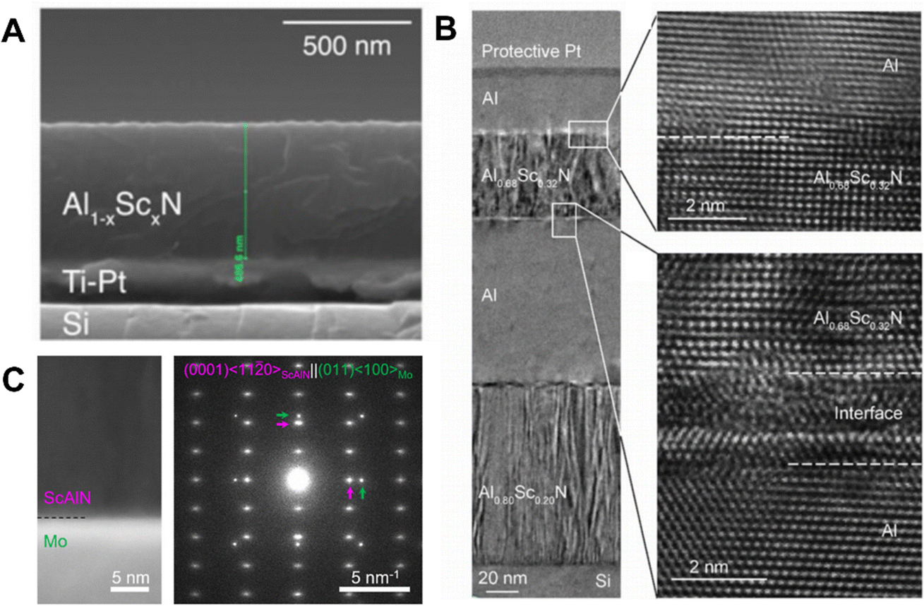 | ||
| Fig. 1 (A) ScAlN-Pt thin film structure grown on Ti–Pt substrates.91 (B) Film structure with Al and ScAlN mutually superposed.45 (C) Structure of ScAlN-Mo thin films grown on Mo.46 | ||
As the CMOS compatibility of Pt is not high and Pt is expensive, other metal-doped thin film structures are reported. Wang et al. reported an Al (30 nm)/Sc0.32Al0.68N (45 nm)/Al (80 nm)/Sc0.20Al0.80N (85 nm)/Si thin film by sputter deposition.92 Its intersecting section SEM was shown in the Fig. 1(B). An atomically sharp interface at the intersection of the ScAlN film and the Al top electrode, while a thicker interface layer is observed at the (Al, Sc) N/bottom Al boundary, which may be related to partial vacuum rupture of the material and exposure of the Al bottom electrode to air before deposition.
In order to make the ferroelectric ScAlN heterostructure compatible with mature CMOS technology, it is necessary to achieve the growth of single crystal ScAlN on metal electrodes. Among the commonly used CMOS-compatible metals, molybdenum has a high melting point (about 2160 °C), low coefficient of thermal expansion (5 × 10⁻⁶ °C−1 at 20 °C), and low resistivity (5 × 10⁻⁸ Ω m), making it an ideal metal for CMOS manufacturing processes. Wang et al. report that the epitaxial growth of III-N heterostructures on molybdenum will provide a viable path to achieving CMOS-compatible ferroelectric nitride and total nitride based complementary circuits, as well as opening up new avenues for integrated, ultra-low loss and UHF acoustic electronic devices (Fig. 1(C)).93
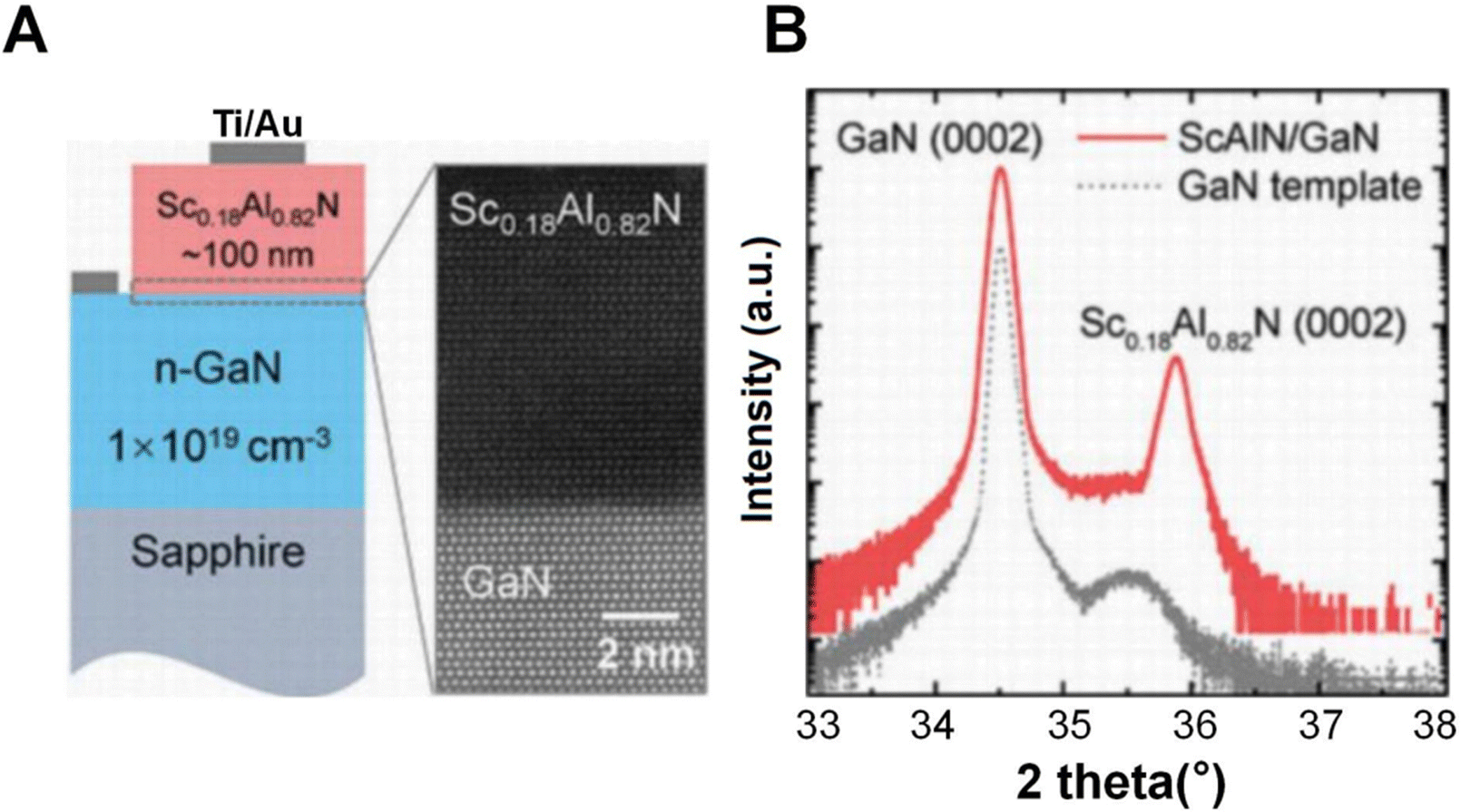
Molecular beam epitaxy (MBE) has several key advantages over traditional sputter deposition for the epitaxy growth of ferroelectric ScAlN, including superior control over crystallinity, stoichiometry, thickness, doping, interface, and uniformity, which are critical for the performance, stability, and yield of memory cells and arrays.17,94 Wang et al. used RF plasma to assist MBE to grow a silicon-doped gallium nitride bottom electrode layer of ≈120 nm and a carrier concentration of ≈1 × 1019 cm−3, and to grow a single crystal ScAlN film with a thickness of ≈100 nm. Ti/Au metal columns of different diameters (3–50 μm) are then deposited as top electrodes, as shown in Fig. 2(A).95 In addition, the results shown are from samples with a gallium nitride electrode carrier concentration of ≈1 × 1019 cm−3 and a top electrode diameter of 20 μm. The Sc content of the ScAlN layer is set to value ≈18% to match the lattice of gallium nitride to reduce mismatch defects and dislocations.96Fig. 2(B) depicts the XRD test results on a ScAlN/n-GaN sample. The characteristic diffraction peak of ScAlN (0002) can be clearly observed, which further confirms the wurtzite structure of ScAlN thin films.12,97 On the other hand, we can observe that the full width half maximum (FWHM) of the (0002) plane rocking curve of the ScAlN film is not more than 400 arcsec, which is much smaller than that of the conventional magnetron sputtered ScAlN film, further confirming its good structural performance.
3.3 Compatibility of ScAlN with memristor technology
Firstly, the excellent photoelectric properties of ScAlN bring higher storage density and faster reading and writing speed to the memristor. The band gap of ScAlN is large, which can absorb visible light and near-infrared light, making it highly sensitive in photoelectric conversion.98 The ScAlN memristor can efficiently perform read and write operations in low light settings, enhancing storage density and reliability.99Secondly, the stable chemical properties of ScAlN provide longer service life and lower power consumption for memristors. ScAlN has stable chemical properties, is not easily affected by environmental factors, and can maintain stable performance in various harsh environments. This makes the ScAlN memristor have a longer service life and reduces maintenance costs. At the same time, due to the low power consumption of ScAlN, the energy consumption of the memristor can be further reduced, making it more in line with the requirements of green environmental protection.
Moreover, the memristor's dependability is ensured by ScAlN's very high thermal stability. ScAlN memristors are more adaptable and reliable since they can keep performing consistently even when exposed to high temperatures.100–102
4. Electrical properties of ScAlN thin films
4.1. The change of electrical properties of AlN doped with rare earth elements
In the study of AlN ferroelectric properties, the doping of rare earth metals is worthy of our attention. Liu et al. made two models of AlN/MoS2 FETs and ScAlN/MoS2 FE-FETs of the same thickness and size to test and compare the electrical characteristics.90 In the test results, we can find that the transmission curve of ScAlN/MoS2 FE-FETs shows a hysteresis loop from clockwise to counterclockwise, indicating the existence of polarization switching(Fig. 3(A)). In contrast, AlN/MoS2 FETs show hysteresis loops only in the clockwise direction, indicating the presence of charge traps but no ferroelectricity (Fig. 3(B)). Fig. 3(C) shows the comparative transfer characteristics of the forward and reverse sweeps of the two models of AlN/MoS2 FETs and ScAlN/MoS2 FE-FETs in the range of ±50 V. Clear and opposite indications of the threshold voltage shift between ScAlN/MoS2 FE-FET and AlN/MoS2 FET for forward (red) and reverse (blue) scans are shown. We can find that the switching current density in ScAlN/MoS2 FE-FETs is significantly higher than that in AlN/MoS2 FETs.103,104 In addition, the threshold voltage shifts of the two types of FETs are also different, indicating the existence of ferroelectric polarization in ScAlN/MoS2 FE-FETs. In summary, the doping of Sc can significantly improve the ferroelectric properties of AlN, which makes it possible for its application in memristors.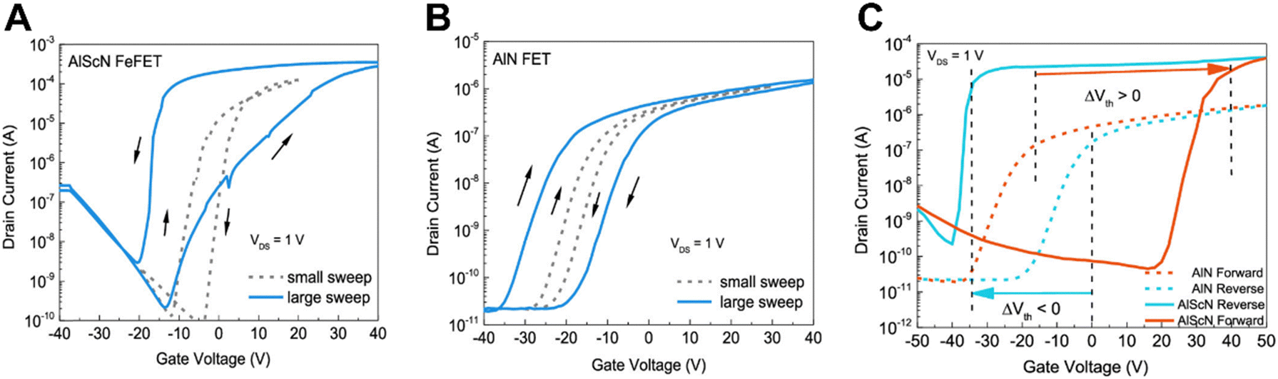 | ||
| Fig. 3 Comparison of the ScAlN/MoS2 FE-FET with the reference AlN/MoS2 FET.43 (A), (B) Transport characteristics of representative ScAlN/MoS2 FE-FET and AlN/MoS2 FE-FET in semilogarithmic scale at room temperature with larger gate voltage sweep range (solid blue line) and smaller gate voltage sweep range (gray dashed line). Film thickness is 100 nm and the channel length is about 3.75 μm. (C) Comparison of the transfer characteristics of ScAlN and AlN dielectric molybdenum disulfide FET during forward and reverse ward scans in the ±50 V range. | ||
Furthermore, we investigated the effect of the Sc doping ratio on the ferroelectric properties of ScxAl1−xN. Based on the study of Simon Fichtner et al., the residual polarization (Pr) of ScAlN can be very high (80–115 μC cm−2) when the proportion of Sc doping exceeds 27%.105,106 Significantly higher than the theoretical predictions for the spontaneous polarization of pure AlN (10 μC cm−2) and 30 μC cm−2 (X = 0.5) with the zinc-blende structure as a reference (Fig. 4(A)).107 The key advantage of the high residual polarization is that the instability caused by charge trapping and leakage current through the ferroelectric insulator has no significant effect on the performance of the FE-FET device. It is pointed out in the report that the large stress field (Ec) and residual polarization (Pr) of ScAlN may be related to the large energy barrier of the material itself, the good uniformity of the internal composition and the wurtzite structure. As the Sc content increases, the switching barrier (u = ½) gradually decreases, resulting in a linear decrease in the stress field from more than 4 MV cm−1 (Al0.73Sc0.27N) to less than 2 MV cm−1 (Al0.57Sc0.43N), and the test results are shown in Fig. 4(B). On the other hand, the partial pressure of the sputtering gas and the stress field (Ec) of ScxAl1−xN vary linearly, similar to those reported for pure AlN.108,109
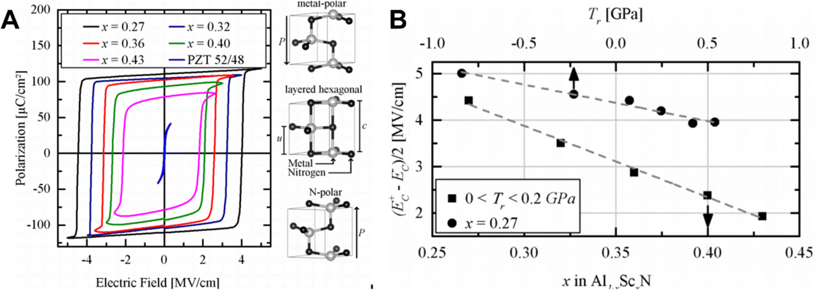 | ||
| Fig. 4 (A) Ferroelectric ScxAl1−xN with Sc contents of 0.27, 0.32, 0.36, 0.46, 0.43 and 0.43 and PZT is the P–E ring of ScxAl1−xN.105 (B) Dependence of the average stress field on the residual stress Tr and Sc content of Al1−xScxN films. Sc content and Tr content vary independently.105 | ||
In conclusion, we found that the expected switching voltage can be obtained by changing the Sc doping ratio and the mechanical stress of the film. It is further demonstrated that ScAlN can achieve low switching voltages in the range (<10 V) relevant for memory applications.
4.2. Long-term cycle durability and C–V test of ScAlN
Through the previous experiments, we can find that the ScAlN material has the characteristics of large current switching ratio, high residual polarization, adjustable internal voltage and so on. In order to further explore the possibility of its application in memristors, we further explore its durability. Liu et al. tested the switching durability of a ferroelectric switch of the Al0.68Sc0.32N material, whose material structure as well as TEM images are shown in Fig. 5(A) and (B).110 The PUND results for Al0.68Sc0.32N show a residual polarization value of 120 μC cm−2, as shown in Fig. 5(C), which is similar to the previous experimental results and confirms the reliability of the experimental data. In Fig. 5(D), the material is subjected to a durability test for switching between the positive and negative polarization states. Both the positive and negative polarization states are stable and rewritable over 20![[thin space (1/6-em)]](https://www.rsc.org/images/entities/char_2009.gif) 000 PUND cycles, demonstrating the durability of the material. In Fig. 5(E), the bottom of the material is grounded, and the top is repeatedly applied with a positive/negative voltage to observe the change in the switching of the material in the high/low configuration. In the long-term voltage switching test, the device shows ultra-low operating current and self-rectifying behavior, which makes it possible for the memristor based on ScAlN without additional transistors or selectors. Fig. 5(F) shows the distribution of LRS and HRS resistance of the device. It can be seen that the high and low resistance states of Al0.68Sc0.32N are closely distributed in the long-term test, which avoids the misreading of the device and ensures the recognition rate of device switches. To sum up, the long-term stable high-low resistance state switching of ScAlN material in electrical testing ensures its durability in memristor devices.
000 PUND cycles, demonstrating the durability of the material. In Fig. 5(E), the bottom of the material is grounded, and the top is repeatedly applied with a positive/negative voltage to observe the change in the switching of the material in the high/low configuration. In the long-term voltage switching test, the device shows ultra-low operating current and self-rectifying behavior, which makes it possible for the memristor based on ScAlN without additional transistors or selectors. Fig. 5(F) shows the distribution of LRS and HRS resistance of the device. It can be seen that the high and low resistance states of Al0.68Sc0.32N are closely distributed in the long-term test, which avoids the misreading of the device and ensures the recognition rate of device switches. To sum up, the long-term stable high-low resistance state switching of ScAlN material in electrical testing ensures its durability in memristor devices.
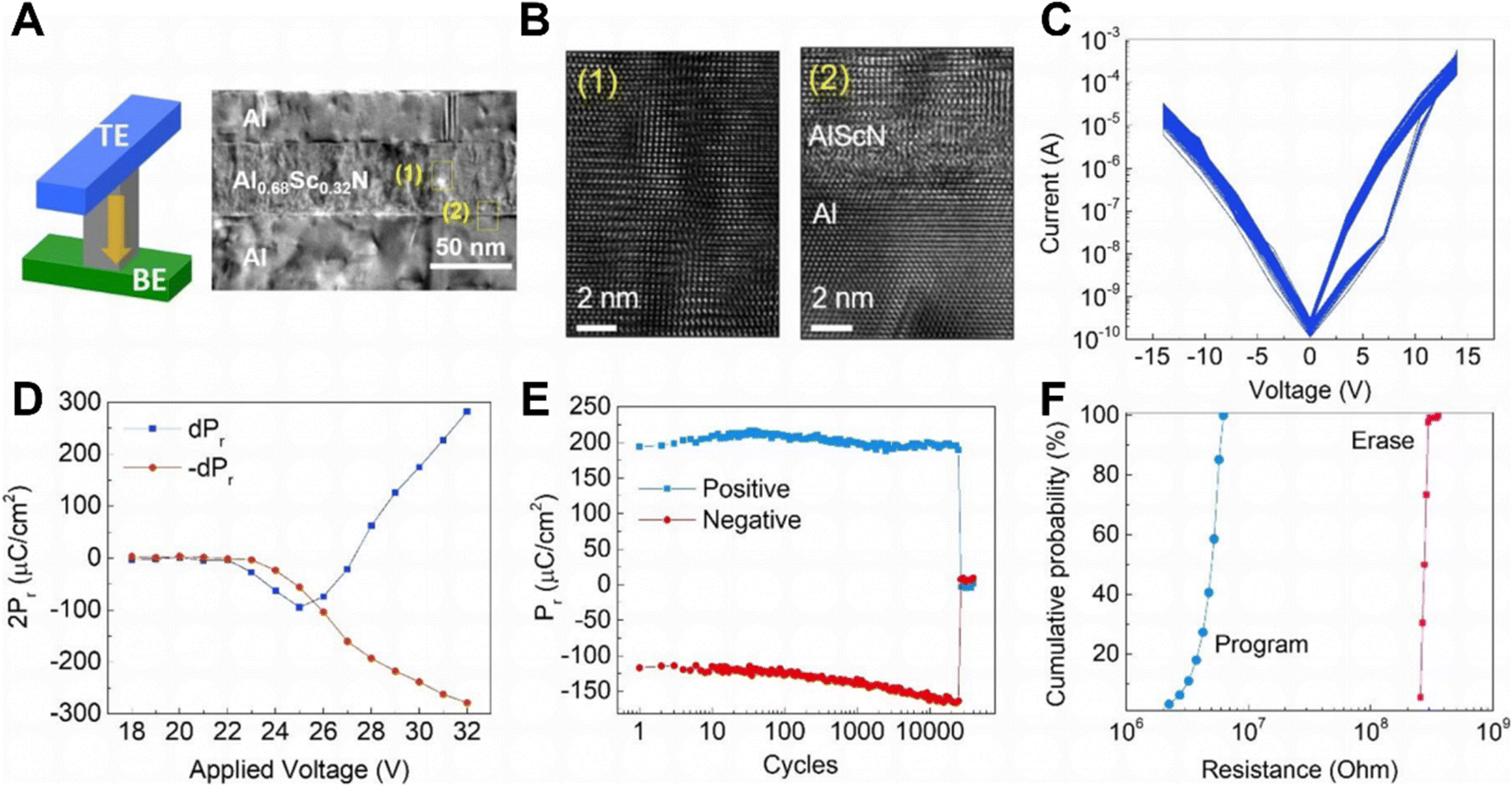 | ||
| Fig. 5 Room temperature electrical properties of ScAlN.11 (A), (B) Three-dimensional schematic of ScAlN FeD device and cross-sectional TEM image of ScAlN FeD showing 45 nm ScAlN as ferroelectric switching layer. (C) PUND results. PUND test shows that the saturated residual polarization is 150 μC cm−2. (D) Residual polarization extracted from PUND measurements in a durability test using an ScAlN film with 1.5 μs pulse width and 26 V amplitude. (E) 100 cycles of program and erase measurements on a 45 nm ScAlN based fed. (F) Distribution of HRS and LRS resistance during the measurement. | ||
To further visualize the switching of the polarization state of ScAlN, Wang et al. performed CV tests on ScAlN-Mo heterostructures of single crystals.93Fig. 6(A) shows the positive (#1, first sweep) and bipolar (# 2, second sweep) C–V measurements on the two original ScAlN capacitors with an AC signal voltage of 100 mV at 1 MHz, Fig. 6(B) shows the negative #1 test, and the rest of the test parameters are the same as Fig. 6(B). We can observe in the bipolar scan (#2) in both figures that the sudden decrease of capacitance during the scan, thus forming a butterfly-shaped test loop (bipolar switchable polarization of ScAlN), indicates that the ferroelectric switching behavior of ScAlN occurs in the scan switch. The difference between the two figures is that in the positive test (#1) of Fig. 6(A), the capacitance scan is completely overlapped, while in the negative test (#1) of Fig. 6(B), there is a significant capacitance drop, thus forming a complete loop. Based on the above phenomenon, we can infer that ScAlN has a uniform downward polarization state, that is, we need a negative voltage to achieve the polarization switching of ScAlN. The capacitance fluctuation of ScAlN can be ignored in the CV test, which shows that ScAlN is a wake-up free ferroelectric nitride semiconductor and has great application potential in ferroelectric memristors, filters and so on.72,111
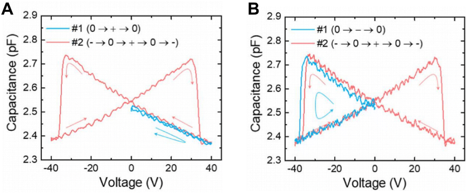 | ||
| Fig. 6 (A), (B) Unipolar (# 1, first sweep) and bipolar (# 2, second sweep) C–V measurements (AC = 100 mV, small signal voltage of 1 MHz) on two pristine ScAlN capacitors to visualize the as-grown polarization state. Scan direction is marked by an arrow in (A), (B).46 | ||
4.3. Assessment of electrical properties for memristor device suitability
As a wide band gap semiconductor material, the electrical properties of ScAlN have attracted much attention in the field of memristors. ScAlN has high electron mobility and high conductivity, which makes ScAlN memristors have great potential in achieving high-speed and low-power storage.Firstly, the high electron mobility of ScAlN means that it has high conductivity. When the current passes through the ScAlN material, the electron moves faster, thereby improving the response speed of the memristor. This makes the ScAlN memristor have advantages in processing high-speed signals and achieving high-speed storage.
Secondly, the high conductivity of ScAlN makes it advantageous in achieving low power consumption. Compared with other semiconductor materials, ScAlN has a lower resistance, which means that at the same voltage, the current through the ScAlN material is larger, thereby reducing power consumption. This is of great significance for achieving low-power electronic products and extending the life of the device.
In addition, the electrical properties of ScAlN also show good stability and repeatability. Through appropriate process control and technical optimization, ScAlN memristors with stable performance and good repeatability can be obtained. This provides a guarantee for ScAlN in applications with long-term storage and high reliability requirements.
In summary, the ScAlN thin film shows very good electrical properties. In order to more intuitively measure the potential of ScAlN as a memristor switching device, Liu et al. compared the electrical test results of Sc0.36Al0.64N thin film and traditional oxide materials (Table 1). We can see that ScAlN materials have better CMOS compatibility, while exhibiting larger switching ratios and thinner thicknesses. This report demonstrates that oxide layers are not necessary or important to demonstrate the iron diode effect, and that nitride materials are also one of the directions for switching devices.
5. Synaptic device simulation and working state of ScAlN thin films
5.1. Overview of current research on ScAlN in synaptic device simulation
In the traditional oxide-based ferroelectric memristor, the oxygen vacancies on the contact surface of the electrode will continue to migrate and accumulate under long-term switching action, which makes the material structure unable to maintain a stable state, which hinders the long-term use of the oxide-based ferroelectric memristor.120,121 The high residual polarization (70–120 μC cm−2), non-wake-up, non-volatile state, and low nitrogen vacancy formation energy of ScAlN-based memristors allow them to exhibit higher durability potential than oxide-based ferroelectric memristors.122,123Recently, ScAlN has achieved a significant advancement in artificial synaptic devices. This semiconductor material, possessing exceptional physical features, offers new opportunities for replicating biological synaptic functions.
Researchers have created novel artificial synaptic devices by utilizing the high electron mobility and stable chemical characteristics of ScAlN in structural design. The performance of ScAlN artificial synapses has been greatly enhanced by implementing a unique multi-layer structure, nanowire technology, and heterojunction design.124–127 These structural improvements not only improve the response speed and memory capacity of artificial synapses, but also enhance their stability in complex environments.
Secondly, the progress of preparation technology is another key aspect of the research progress of ScAlN. With the development of thin film preparation technology, such as pulsed laser deposition and magnetron sputtering technology, high quality ScAlN thin films have been successfully prepared.128 This laid the foundation for the large-scale production and integration of artificial synaptic devices. At the same time, advanced nanofabrication technology has also been applied to the fine processing of ScAlN artificial synapses, further improving the performance and reliability of the device.
Furthermore, the utilization of ScAlN artificial synapses in developing intelligent information processing systems has advanced significantly. ScAlN artificial synapses have significant promise in pattern recognition, image processing, and speech recognition due to the integration of neural networks with machine learning techniques. The applications demonstrate the significant capabilities of ScAlN artificial synapses in advanced information processing.
5.2. Spike-timing-dependent plasticity (STDP) and switching behavior in ScAlN as a synaptic device
To investigate the potential application of ScAlN in memristors, Wang et al. fabricated ferroelectric GaN/ScAlN heterostructure memristors for synapse simulation. 20 nm thick Si-doped n-type GaN (electron concentration ∼1 × 1018 cm−3) was grown on top of 100 nm thick ScAlN.93 Firstly, Fig. 7(A) shows the structure of the memristor, with ScAlN and Mo corresponding to the front end of the synapse (sending signals), and GaN and Ti/Au/Ti corresponding to the back end of the synapse (receiving signals). Fig. 7(B) and (C) show the band diagram of GaN/ScAlN heterostructure. Due to the ferroelectric field effect, the polarization direction of ScAlN changes with the barrier height (Φ) of the interface. The ScAlN is polarized down to increase the barrier height (Φdown) by filling the GaN with negative charge, corresponding to the OFF state. Correspondingly, the upward polarization of ScAlN accumulates positive charge in GaN, thereby reducing the barrier height (Φup), corresponding to the ON state. Through the analysis of the band structure of GaN/ScAlN heterostructure, two obviously different barrier heights (Φup and Φdown) demonstrate the possibility of realizing resistive switching.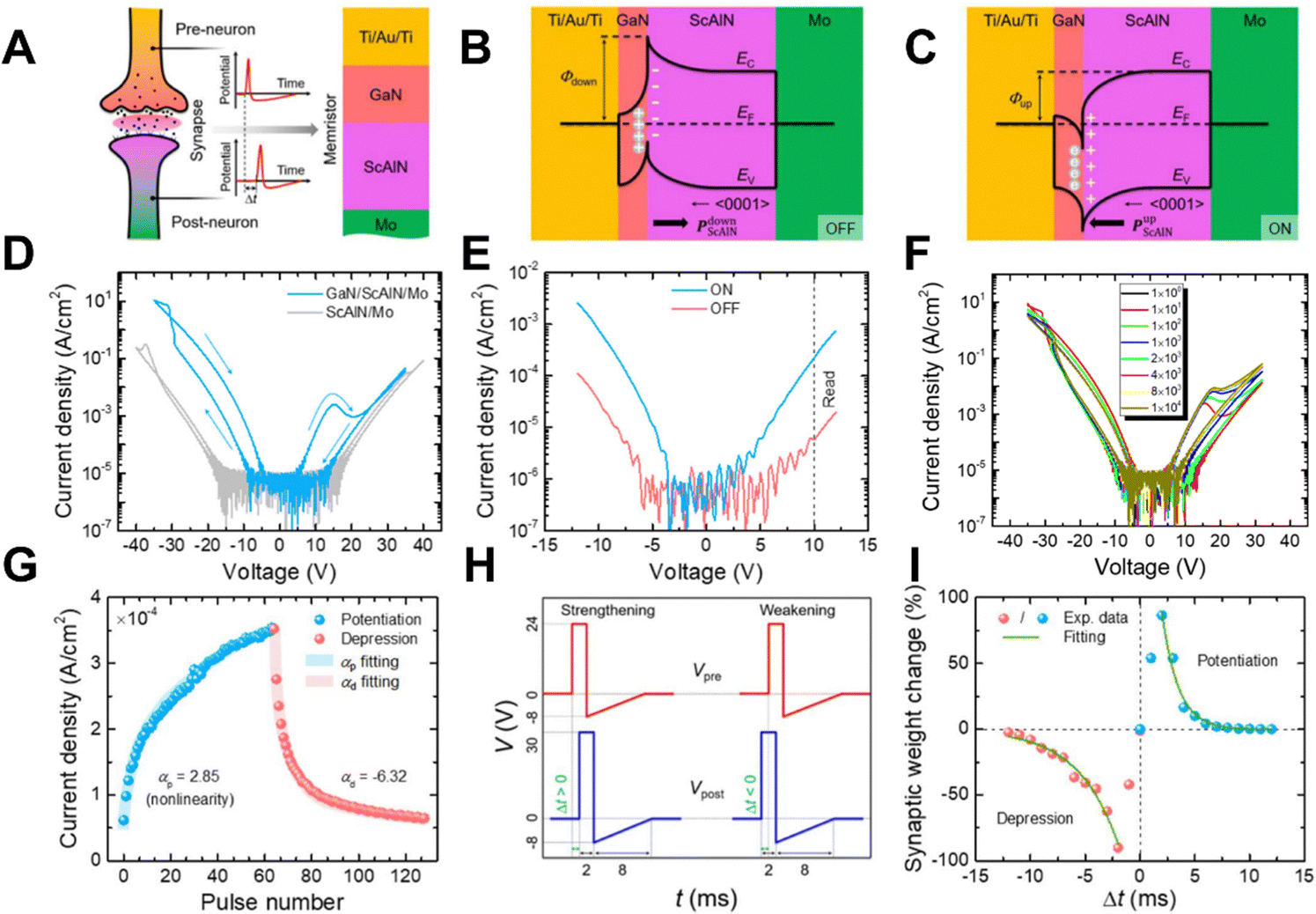 | ||
| Fig. 7 Ferroelectric GaN/ScAlN heterostructure memristor for synapse simulation.46 (A) Sketch of a pre-neuron and a post-neuron connected by synapses, and a resistive memristor based on a ferroelectric GaN/ScAlN heterostructure on Mo. (B) and (C) Band diagram (zero bias) modulation by ferroelectric polarization switching in GaN/ScAlN structures. (D) Typical J–V loop measured by GaN/ScAlN memristive resistance (blue curve) and ScAlN capacitor (gray curve) in steps of 0.1 V. The sweep direction is marked by an arrow (+ →0 → − → 0 → +). (E) On/off current density measured in a small voltage range. (F) On/off current density measured after multiple cycles. (G) Evolution of the GaN/ScAlN memristor conductance as a function of the same number of pulses, showing enhancement and suppression features. (H) Voltage waveforms used to simulate the voltage peaks of the pre-neuron (red) and post-neuron (blue) for a total length of 10 ms. (I) Variation of ferroelectric GaN/ScAlN memory-based artificial synapse with respect to delay time (Δt). | ||
In the previous paper, we demonstrated the possibility of ScAlN as the memristor material to realize resistance switching, and we need to further study the electrical properties of resistance switching behavior. The resistive switching behavior of the GaN/ScAlN heterostructure was characterized by quasi-static J–V measurements (Fig. 7(D)), showing clear bipolar hysteresis. In Fig. 7(D), ScAlN/Mo is shown as comparative data (gray curve). We can find that the intervention of GaN makes the on and off currents have more obvious separation (blue curve). It can be seen that the multilayer heterostructure GaN/ScAlN has better resistance switching ability than the single layer ScAlN.
Fig. 7(E) further plots the measured data for the on and off currents measured in a small voltage range, and we find distinct ON and OFF states with an on/off ratio of about 40 at a read voltage of +10 V. The conductivity of the memory resistor can be continuously modulated by applying either negative voltage or positive voltage pulses, demonstrating its conductance plasticity capability.
Fig. 7(F) shows the J–V measurements of the memristor after a long switching cycle. The on/off ratio decreases from 40 to about 10 after 1 × 10³ cycles. After 1 × 10⁴ cycles, the switching period of the ferroelectric polarization induced shift current peak can still be clearly observed, which indicates that the fatigue behavior of the memory window is mainly due to the degradation of the heterointerface rather than the ferroelectric polarization switching fatigue. Ferroelectric GaN/ScAlN heterostructure memristors show potential for synaptic simulation and artificial neural network applications. ScAlN has better durability and wake-up free behavior than oxide-based ferroelectric memristors. Further research is needed to improve the endurance of memristors and explore their potential in neuromorphic computing.
In general, memristor conductance can be regarded as the strength of a synapse.129–131 Thus, an increase (decrease) in electrical conductivity corresponds to an enhancement (inhibition) in the strength of synaptic connections. In the GaN/ScAlN heterostructure, the conductance of the ScAlN memristor is gradually adjusted by 64 long-term positive/negative pulse voltages (Fig. 7(G)), and we can find that the conductance is linearly enhanced and inhibited, confirming the plasticity of the conductance (synaptic strength). In order to further observe the plasticity of the synaptic strength of the ScAlN memristor, we applied pulses with different arrival times before and after the synapse to the device to test whether it had STDP behavior. The voltage waveforms used to simulate the voltage peaks of the pre-neuron (red) and the post-neuron (blue) are presented in Fig. 7(H), with a total length of 10 ms, and we can see two waveforms with a delay time (Δt) greater than zero and less than zero. The results of synaptic weight changes based on ferroelectric GaN/ScAlN memristors at different delay times (Δt) are shown in Fig. 7(I). It is found that synaptic potentiation occurs when the presynaptic impulse arrives earlier than the postsynaptic impulse (Δt > 0), and synaptic depression occurs when the postsynaptic impulse arrives earlier than the presynaptic impulse (Δt < 0). That demonstrates that ferroelectric GaN/ScAlN based memristors possess STDP (spike timing dependent plasticity).132–134
5.3. Simulation calculation of the neural network in ScAlN devices
To further explore the possibility of practical application of ScAlN memristors, Wang et al. simulated the memristor synapse based on the single crystal ScAlN epitaxial on GaN, and demonstrated its working state and recognition rate in image recognition and reproduction through convolution algorithms.135In Fig. 8(A), eight clearly discernible conduction states are successfully demonstrated in the ScAlN memristor by a gradually increasing pulse voltage scheme. The eight conductance states are linearly and regularly distributed, which shows the controllability of the internal conductance of the material. Fig. 8(B) shows that these conduction states can be recovered after multiple program/reset operations and remain stable within 200 seconds, demonstrating the reliability of the device under multiple pulses and cycles. Fig. 8(C) shows a schematic of a logarithmic drive, where the nonlinear device voltage, Vde, is extended to a linear drive voltage, Vdr, by the calculation of the mapping function for β = −1.75 and C = 3.2. Fig. 8(D) shows the mapping results, where the linear effective conductance is reached for all conductance levels. The circuit conversion of nonlinear to linear data is similar to a real p–n junction or Schottky barrier diode.136 Based on the mapping method of Fig. 8(C) and (E) shows a demonstration of multi-state and convolution operations using nitride memristors. In this figure, the input of the grayscale image is encoded as voltage pulses from −2.05 V to −2.98 V, and the output is weighted according to eight admittance states. The weighted output for each input pixel intensity can be viewed as the result of the multiplication of a 1 × 1 vector by a 1 × 1 matrix (pixel intensities multiplied by weights). The demonstration of linear VMM operation can be simulated by establishing a linear effective admittance on a nonlinear nitride memristor with the correct choice of fitting parameters. In Fig. 8(F), the memristor shows the results of a basic image convolution operation using three different convolution kernels. Grayscale image of 100 × 100 pixels was used as the input image, and three 3 × 3 convolution kernel operations (averaging, edge, and sharpening) were performed. These results indicate that ScAlN-based memristors can be used for convolution operations for image processing and feature extraction. Fig. 8(G) compares the simulation accuracy of a two-layer MLP based on an ideal device (black, 128 conductance states, on/off ratio of 50, perfect linearity) with those based on a ScAlN memory with nonlinear properties (blue) and further considering intra-cycle variations and inter-device variations (green). (Specific experimental parameters can be found in ref. 135.) The best recognition accuracy of the ScAlN memristor with nonlinearity and intra-/inter-device variation is 92.9%, which is still far from the recognition accuracy of the ideal device (96.2%), but the ScAlN memristor has shown better performance than most analog salient devices.
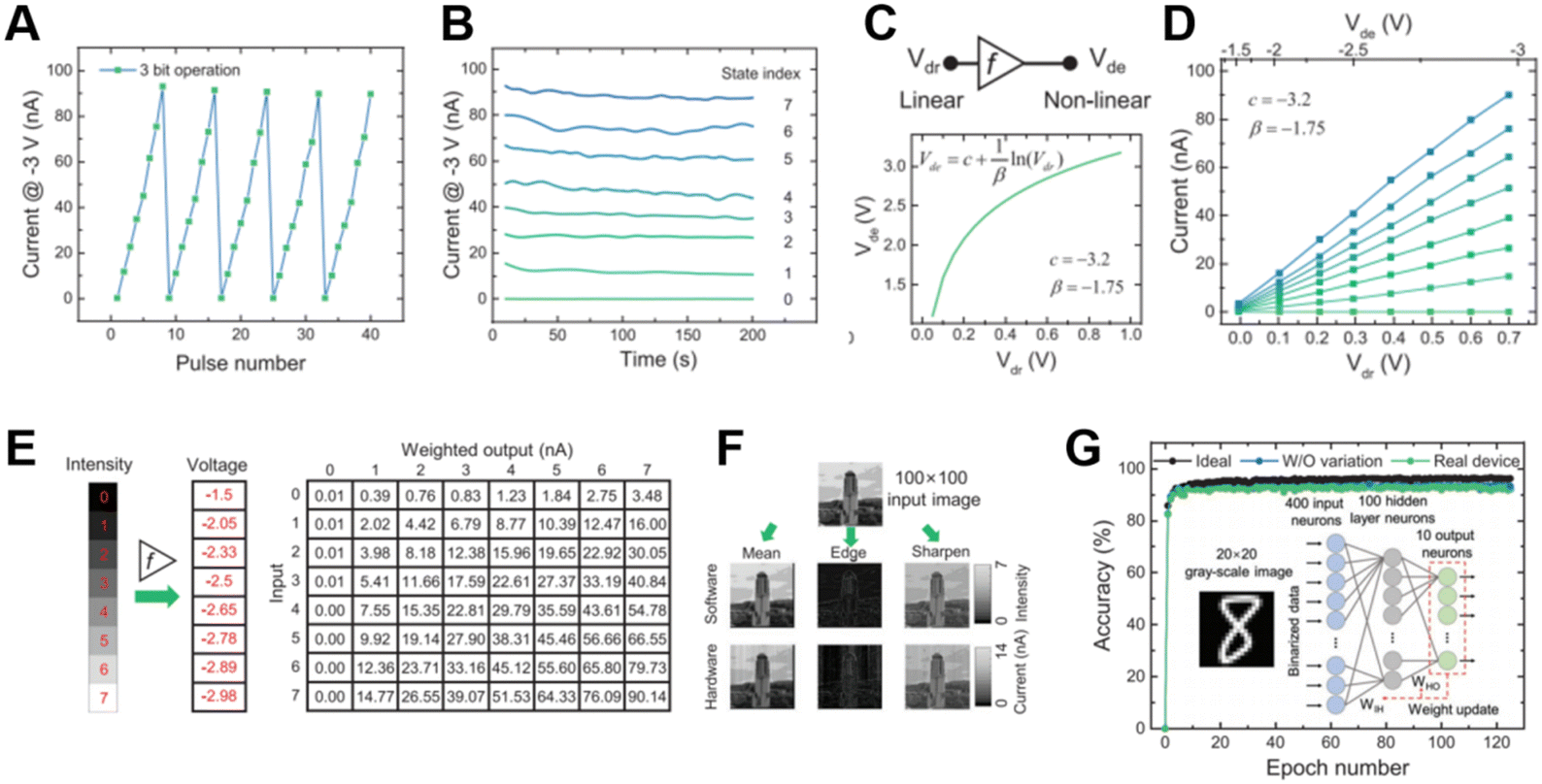 | ||
| Fig. 8 (A) Multi-state operation from −8 V to −8.35 V by incremental pulses in steps of −50 mV with a read voltage of −3 V. Pulse width is 8 ms.78 (B) Current variation with 8 states retained for 200 s.78 (C) and (D) Schematic of a logarithmic driver that maps a linear input voltage to the nonlinear input of a nonlinear nitride memory transistor. By choosing the fitting parameters properly, the linear effective conductance of the simulation calculation can be established.78 (E) Grayscale image input for the convolution operation. Brightness of each pixel is encoded as a voltage pulse from −2.05 V to −2.98 V, which gives a weighted output based on 8 conductance states.78 (F) Basic image convolution operation for three different kernels using the ferrielectric nitride memory. A grayscale image with 100 × 100 pixels is used as the input image. Three 3 × 3 kernel operations (average, edge, and sharpen) are provided as examples.78 (G) Comparison of the accuracy of the two-layer MLP simulation based on the ideal device (black, 128 States, on/off ratio 50, perfect linearity) and based on the ScAlN memristor (blue) and further cyclic variations and inter-device variations (green).78 | ||
5.4. Applications of innovative integrated arrays in ScAlN devices
The convolutional neural network (CNN) extracts the features of the learning target by constantly adjusting the weight value, so as to achieve the purpose of deep learning.137 Traditional memristor structures generally require a large number of inputs, memristors and selectors for multiple convolution calculations, in which a large amount of data is calculated and transported.138–141 Therefore, how to reduce the cost of memristor by simplifying the device structure is also a hot research direction.Liu et al. studied a transistor-free ScAlN-based ferroelectric diode array, which realizes data storage, search and neural network operation on sub-50 nm thick FeDs.110 In this study, the authors designed a fully BEOL compatible architecture using two ScAlN field-programmable ferroelectric diodes in parallel. The purpose of this is to use non-volatile memories (NVMs) instead of traditional TCAM to save power and reduce the footprint of the device. The structure is shown in Fig. 9(A).
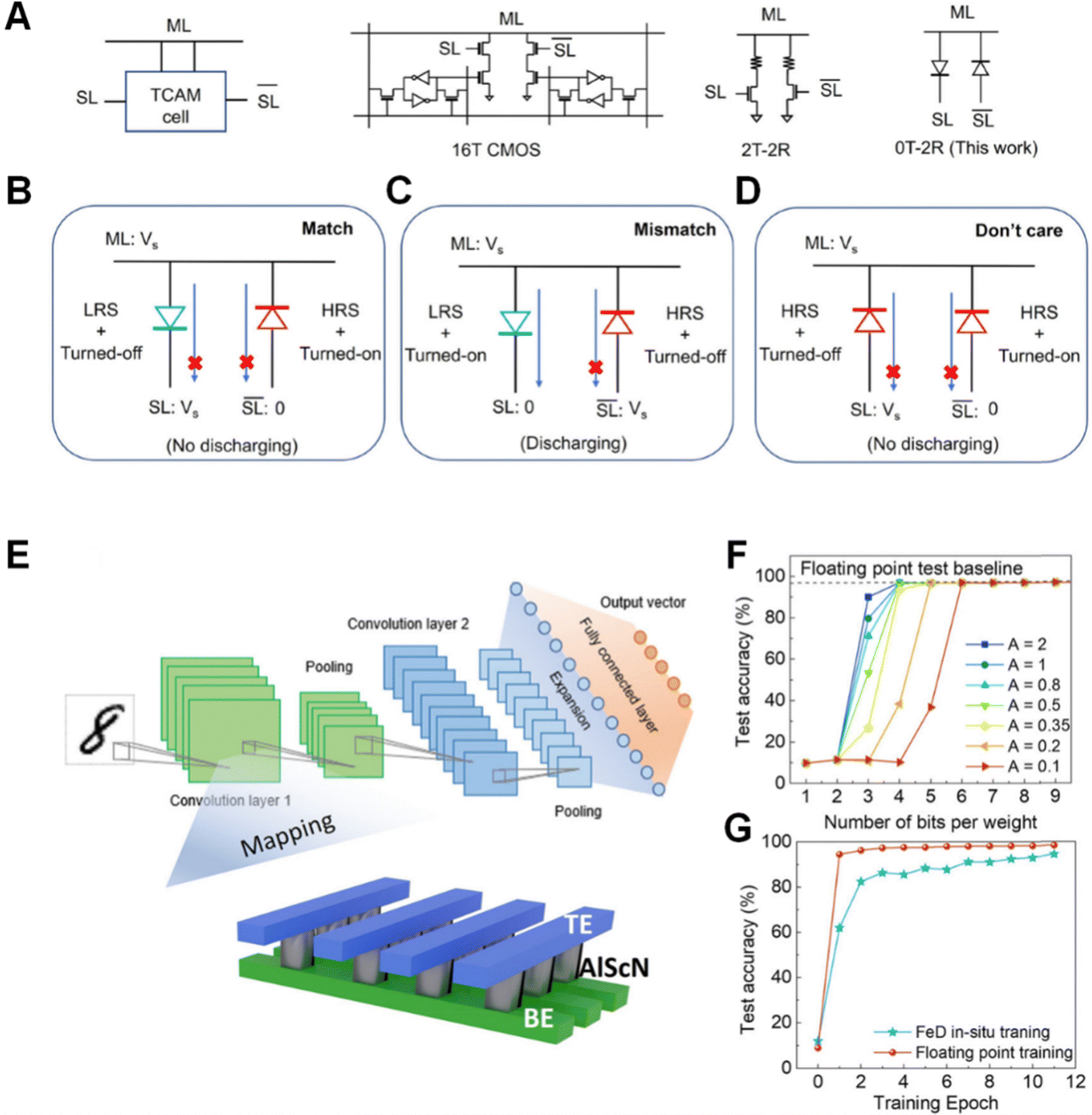 | ||
| Fig. 9 (A) The traditional TCAM unit and the innovative double FED structure.110 (B), (C) and (D) “Matched”, “Mismatched” and “Don’t Care” line states for the three operating modes in the two-FEDs architecture.110 (E) Convolution operation and feature extraction process of convolutional neural network (CNN).110 (F) The recognition accuracy of the device under different nonlinear index A.110 (G) The comparison of the training accuracy and the software recognition accuracy obtained by the device in this study.110 | ||
As shown in Fig. 9(B), we write a logic “1” state into the FeD TCAM cell by programming the left/right FeD to a low-resistance/high-resistance state, respectively. During a search operation, the match lines (MLs) are biased by a read voltage V.sub. S higher than the turn-on voltage of FeD. Next, logic “1” is searched by applying high/low voltages to the search lines (SL and SL), respectively, and vice versa for logic “0”. When the store data and the search data match (as shown in Fig. 9(B), the store bit is logic “1” and the search bit is logic “1”), the FEDs in both the high and low impedance states are in the off state. However, when the search data do not match the stored data, the left side FeD, which has a low resistance state, is turned on due to the high voltage drop between its anode and cathode. Therefore, the discharge current is significant and the ML voltage is low (Fig. 9(C)). Fig. 9(D) also demonstrates the “don’t care” statement in two FeD-based TCAMs, switching both FEDs to a high-resistance state, and the device assumes the “don’t care” statement regardless of any voltage signal. The dual FED architecture with all three states can reduce the search delay compared to conventional TCAM, while also simplifying the device architecture and reducing material costs.
Next, we focus on the application of the FeD device array in deep neural network (DNN) inference/training. In deep learning network computing, more conductance states mean more power overhead at the architecture level, and the selector-free dual-FED array can make the best trade-off between these indicators.136,142 As shown in Fig. 9(E), a convolutional neural network (CNN) is first trained on the MNIST data set and the calculated weight values are extracted. The pre-trained weights in the CNN are then hierarchically quantized by normalizing the weights to the FeD conductance range. In order to quantify the effect of nonlinearity and asymmetry on accuracy loss, a nonlinear index A was established, and the relationship between A-factor and measurement accuracy is shown in Fig. 9(F). We find that sparsely arranged conductance states with superior linearity can replace a large number of conductance states, and the high linearity of the weight distribution in the training phase has a higher recognition rate. In addition, the memory implementation of on-site training on the FeD array is simulated in Fig. 9(G). We find that the device has achieved excellent training accuracy, but the accuracy of field learning is reduced to varying degrees compared with the accuracy of floating-point software training, which shows that there is still room for optimization.
In conclusion, this research realizes the search function by introducing the innovative structure of double FEDS instead of transistors, and demonstrates the neural network under this structure, while the results show that the accuracy is comparable to that of the software. The series of experiments were carried out on FeD devices with a 45 nm thick FE AlScN layer, further demonstrating the potential of ScAlN ferroelectric materials for applications in artificial synapses.
6. Future directions and recommendations
6.1. Summary of key findings
In this paper, the application of ScAlN in memristors is described from the aspects of material mechanism, preparation process and structure, ferroelectric properties and simulation application. Firstly, in the study of material mechanism, the influence of rare earth metal Sc doping on the semiconductor material AlN was discussed. Secondly, we focus on the influence of different preparation processes and structures on the adaptation of ScAlN in memristor devices. In addition, in the discussion of ferroelectric properties, the long-term cycle stability in various electrical tests is mainly concerned. Finally, with regard to the simulation application of ScAlN in memristors, the innovative array structure is focused.6.2. Insights into potential future research directions
Based on the current research summary of ScAlN memristor, there is still much room for further research on the preparation process of materials, the study of synaptic mechanism and the diversification of simulation environment, for which we consider the following prospects7. Conclusions
7.1. Recapitulation of major points
In this paper, the current research progress of ScAlN in memristors is introduced in detail. First of all, a variety of processes and structures to achieve single crystal epitaxial heterojunctions are reported in the fabrication process of ScAlN thin films. Sputter deposition and molecular beam epitaxy are mainly used in the current preparation process. The team of Wang et al. has realized a variety of epitaxial single crystal heterostructures by molecular number epitaxy. Through the study of the thin film structures, we found that ScAlN could be compatible with CMOS, which provides the possibility for its application in integrated devices. Secondly, we investigated the electrical properties of ScAlN films. We found that the doping of Sc can make AlN show superior ferroelectricity, showing a clear polarization switch. At the same time, the Sc doping ratio is further reported, and we find that by adjusting the Sc doping ratio and the pressure of the sputtering gas, the internal stress field (Ec) of ScAlN can achieve the required low switching voltage of the memory device. PUND and C–V measurements were used to explore the ferroelectricity of ScAlN, the heterostructure has great non-volatile memory potential with superior on/off ratio, high uniformity, good retention, and moderate cycling endurance. Finally, we simulate the synapse of the SCAIN-based device. Based on the band structure analysis of the material and the quasi-static J–V measurement, ScAlN shows obvious resistive switching performance and long-term switching cycle stability. Furthermore, we provide linear simulation calculations and image processing tests to simulate its operation as a synaptic device. The device shows obvious STDP and high image recognition rate (92.9%).7.2. Implications of ScAlN applications in memristors
The excellent physical properties (high dielectric constant, low leakage current and good thermal stability) of ScAlN make it an ideal material for memristors.143 The following points are of great significance for improving the performance of memristors.Firstly, by adjusting the composition and structure of ScAlN, the electrical characteristics may be managed to control the resistive behavior of the memristor more effectively. This enhances the potential for adjusting the memristor. Secondly, enhancing the storage density is achieved by utilizing the high dielectric constant of ScAlN to decrease the size of the memristor, thereby boosting the storage density.144 It is crucial for memristors to enable larger-scale, high-density storage applications. Thirdly, via lowering energy consumption: the low leakage current properties of ScAlN aid in decreasing the energy usage of the memristor, enhancing its energy efficiency. This is highly important for decreasing the energy usage of electrical devices and extending their lifespan.
In summary, the emerging ferroelectric material ScAlN has great potential in the application of memristor devices. In the current situation that the performance of oxide-based memristors encounters bottlenecks (the device structure is unstable due to the continuous change of oxygen vacancies under long-term switching cycles), nitride-based memristors are undoubtedly a reliable choice for the new generation of memory computing devices.
7.3. Contribution to advancements in electronic device development
This paper focuses on the study of ScAlN as a memristor material. Its main purpose is to explore the possibility of nitride memristors for design and production. It can make the following contributions to the current development of electronic equipment:First of all, nitride memristors have better non-volatility.145,146 Compared with traditional oxide memristors, they can maintain their storage state even after power failure. This makes it an ideal choice for modern high-performance memory, especially in applications that require continuous data storage, such as embedded systems, mobile devices, and data centers.
Secondly, due to the different energy levels of nitrogen vacancies and oxygen vacancies, nitride memristors require lower energy than oxide memristors when reading and writing data, which makes them an ideal component for low-power electronic devices.147–150 In today's increasingly stringent low-power requirements, this feature is essential for extending the service life of electronic devices and improving energy efficiency.
Besides, in the era of rapid development of AI models, electronic devices can maintain high efficiency and accuracy when processing large amounts of data. The nitride memristor can maintain good performance stability after multiple read and write cycles, which makes it highly reliable in electronic devices. This is of great significance for applications that require high-speed data processing and long-term stable operation, such as servers, medical equipment, graphics processing, and artificial intelligence.151–153
In conclusion, nitride memristors provide strong support for the development of electronic devices due to their unique performance advantages. With the continuous advancement of technology and the expansion of application fields, nitride memristors are expected to play a greater role in the future and promote the development of electronic equipment to scale new heights.
Author contributions
Xin-Gui Tang, Li-Jun Sun and Yan-Ping Jiang designed and proposed the project. Dong-ping Yang was responsible for the data receipt, outline drafting and body writing of the article. Dan Zhang and Hua-Feng Dong co-wrote the manuscript. All authors contributed to the general discussion.Conflicts of interest
The authors declare that they have no conflict of interest.Acknowledgements
This work was financially supported by the National Natural Science Foundation of China (grant no. 11574057 and 12172093) and the Guangdong Basic and Applied Basic Research Foundation (grant no. 2021A1515012607).References
- W. Meng, F. Xu and Z. Yu,
et al., Three-dimensional monolithic micro-LED display driven by atomically thin transistor matrix, Nat. Nanotechnol., 2021, 1231–1236 CrossRef CAS PubMed
.
- Y. Wu, X. Liu and A. Pandey,
et al., III-nitride nanostructures: Emerging applications for Micro-LEDs, ultraviolet photonics, quantum optoelectronics, and artificial photosynthesis, Prog. Quantum Electron., 2022, 85, 100401 CrossRef
- L. Jaloustre, S. Le Denmat and T. Auzelle,
et al., Toward Quantitative Measurements of Piezoelectricity in III-N Semiconductor Nanowires, ACS Appl. Nano Mater., 2020, 43–52 Search PubMed
- J. K. Hite and J. M. Zavada, Dilute Magnetic III-N Semiconductors Based on Rare Earth Doping, ECS J. Solid State Sci. Technol., 2019, 527 CrossRef
- C. R. Eddy, N. Nepal and J. K. Hite,
et al., Perspectives on future directions in III-N semiconductor research, J. Vac. Sci. Technol., A, 2013, 31 Search PubMed
- Y. L. Su, W. H. Kao and K. H. Sung, Mechanical and Tribological Properties of NbAl, NbAlN, and NbAIN-CH Coatings Deposited using Various Niobium Target Currents and Acetylene Flow Rates, J. Mater. Eng. Perform., 2022, 3594–3610 CrossRef CAS
- M. Benkahoul, M. K. Zayed and C. S. Sandu,
et al., Structural, tribo-mechanical, and thermal properties of NbAlN coatings with various Al contents deposited by DC reactive magnetron sputtering, Surf. Coat. Technol., 2017, 172–178 CrossRef CAS
- R. Franz, M. Lechthaler and P. Polcik,
et al., Tribological Properties of Arc-Evaporated NbAlN Hard Coatings, Tribol. Lett., 2011, 143–152 Search PubMed
- K. Liu, H. Sun and F. AlQatari,
et al., Wurtzite BAlN and BGaN alloys for heterointerface polarization engineering, Appl. Phys. Lett., 2017, 111 Search PubMed
- Y. Ota, M. Imura and R. G. Banal,
et al., Natural band alignment of BAlN and BGaN alloys, J. Phys. D: Appl. Phys., 2022, 55 Search PubMed
- Y. Dong, W. Lin and J. Yan,
et al., Lattice and electronic structures of BAlN in the deep ultraviolet spectral region, Phys. B, 2021, 619, 413188 CrossRef CAS
- S. Yasuoka, T. Shimizu and A. Tateyama,
et al., Effects of deposition conditions on the ferroelectric properties of (Al1−xScx)N thin films, J. Appl. Phys., 2020, 128 Search PubMed
- M. G. Ancona, Nonlinear Thermoelectroelastic Analysis of III-N Semiconductor Devices, IEEE J. Electron Devices Soc., 2017, 320–334 CAS
- W. Thomas, Z. Mohammad and K. Golta,
et al., Interfacial adhesion strength of III-N heterostructures, Mater. Des., 2021, 213, 110319 Search PubMed
- C. Ostermaier, P. Lagger and M. Reiner,
et al., Review of bias-temperature instabilities at the III-N/dielectric interface, Microelectron. Reliab., 2018, 62–83 CrossRef CAS
- P. Wang, D. Wang and Y. Bi,
et al., Quaternary alloy ScAlGaN: A promising strategy to improve the quality of ScAlN, Appl. Phys. Lett., 2022, 120 CAS
- P. Wang, D. A. Laleyan and A. Pandey,
et al., Molecular beam epitaxy and characterization of wurtzite ScxAl1−xN, Appl. Phys. Lett., 2020, 116 Search PubMed
- J. Sun, J. Zhang and J. Yan,
et al., Ferroelectricity and Piezoelectric Response of (Sc,Y)N/(Al,Ga,In)N Monolayer Alternating Stacked Structures by First-Principles Calculations, Phys. Status Solidi B, 2022, 259(8), 2200079 CrossRef CAS
- V. Yoshioka, J. Lu and Z. Tang,
et al., Erratum: “Strongly enhanced second-order optical nonlinearity in CMOS-compatible Al1−xScxN thin films” [APL Mater. 9, 101104 (2021)], APL Mater., 2022, 9–11 Search PubMed
- Y. Chen, Y. Wang and Y. Luo,
et al., Realization of Artificial Neuron using MXene Bi-Directional Threshold Switching Memristors, IEEE Electron Device Lett., 2019, 1686–1689 CAS
- L. O. Chua, Nonlinear circuit foundations for nanodevices, part I: the four-element torus, Proc. IEEE, 2003, 1830–1859 CrossRef CAS
- J. M. Tour and T. He, Electronics: The fourth element, Nature, 2008, 205–211 Search PubMed
- R. Thangavel, B. K. Ganesan and V. Thangavel,
et al., Emerging Materials for Sodium-Ion Hybrid Capacitors: A Brief Review. ACS Applied Energy, Materials, 2021, 4(12), 13376–13394 CAS
- D. Sui, M. Chang and Z. Peng,
et al., Graphene-Based Cathode Materials for Lithium-Ion Capacitors: A Review, Nanomaterials, 2021, 25–39 Search PubMed
- O. G. Gnonhoue, A. Velazquez-Salazar and É. David,
et al., Review of Technologies and Materials Used in High-Voltage Film Capacitors, Polymers, 2021, 766 CrossRef CAS PubMed
- D. W. Braudaway, Precision resistors: a review of material characteristics, resistor design, and construction practices, IEEE Trans. Instrum. Meas., 1999, 878–883 CrossRef
- D. Mills, A Review of Thin Film Resistors and Their Assembly Problems, Microelectron. Int., 1988, 42–45 Search PubMed
- M. S. Perdigao, M. F. Menke and A. R. Seidel,
et al., A Review on Variable Inductors and Variable Transformers: Applications to Lighting Drivers, IEEE Trans. Ind. Appl., 2016, 531–547 Search PubMed
- O. F. Hikmat and M. S. R. F. Mohamed Ali, MEMS Inductors and Their Applications—A Review, J. Microelectromech. Syst., 2017, 17–44 CAS
- C. Li, L. Chen and L. Minghua,
et al., Scandium-Doped Aluminum Nitride for Acoustic Wave Resonators, Filters, and Ferroelectric Memory Applications, ACS Appl. Electron. Mater., 2022, 612–622 CAS
- X. Liu, J. Zheng and D. Wang,
et al., Aluminum scandium nitride-based metal–ferroelectric–metal diode memory devices with high on/off ratios, Appl. Phys. Lett., 2021, 118–127 CAS
- S. C. Mahyar and B. C. Pierre, Memristor nanodevice for unconventional computing:review and applications, arXiv, 2017, preprint DOI:10.48550/arXiv.1703.00331.
- K. Rafailia-Eleni, F. Iosif-Angelos and N. Vasileios,
et al., Memristors in Cellular-Automata-Based Computing: A Review, Electronics, 2023, 107–123 Search PubMed
- Y. Li, Z. Wang and R. Midya,
et al., Review of memristor devices in neuromorphic computing: materials sciences and device challenges, J. Phys. D: Appl. Phys., 2018, 51, 503002 CrossRef
- H. Liu, M. Wei and Y. Chen, Optimization of Non-linear Conductance Modulation Based on Metal-Oxide Memristors (A Review), Nanotechnol. Rev., 2018, 443–468 CrossRef CAS
- M. Patel, N. R. Hemanth and J. Gosai,
et al., MXenes: promising 2D memristor materials for neuromorphic computing components, Trends Chem., 2022, 835–849 CrossRef CAS
- S. Pi, C. Li and H. Jiang,
et al., Memristor crossbar arrays with 6-nm half-pitch and 2-nm critical dimension, Nat. Nanotechnol., 2018, 35–39 Search PubMed
- X. Yan, Q. Zhao and A. P. Chen,
et al., Vacancy-Induced Synaptic Behavior in 2D WS2 Nanosheet–Based Memristor for Low-Power Neuromorphic Computing, Small, 2019, 109–127 Search PubMed
- C. Hao, T. Xin-Gui and S. Zhihao,
et al., Emerging memristors and applications in reservoir computing, Front. Phys., 2023, 59–72 Search PubMed
- C. Zhi-Long, X. Yang and H. Wen-Yuan,
et al., In-sensor reservoir computing based on optoelectronic synaptic devices, Appl. Phys. Lett., 2023, 123, 100501 CrossRef
- H. Kenji, K. Shoya and Y. Hiroshi,
et al., Spontaneous Polarization and Polarization-Induced Electron Sheet Charge of YbAlN on GaN: A First-Principles Study, ACS Appl. Electron. Mater., 2022, 4772–4780 Search PubMed
- K. Furuta, K. Hirata and S. A. Anggraini,
et al., First-principles calculations of spontaneous polarization in ScAlN, J. Appl. Phys., 2021, 130, 024104 CrossRef CAS
- R. Khan, N. U. Rehman and N. Ilyas,
et al., Threshold switching in nickel-doped zinc oxide based memristor for artificial sensory applications, Nanoscale, 2022, 1900–1913 Search PubMed
- R. Khan, N. Ilyas and M. Z. M. Shamim,
et al., Oxide-based resistive switching-based devices: fabrication, influence parameters and applications, J. Mater. Chem. C, 2021, 15755–15788 RSC
- N. Ilyas, J. Wang and C. Li,
et al., Nanostructured Materials and Architectures for Advanced Optoelectronic Synaptic Devices, Adv. Funct. Mater., 2021, 32, 2110976 CrossRef
- M. T. Hardy, B. P. Downey and N. Nepal,
et al., Epitaxial ScAlN grown by molecular beam epitaxy on GaN and SiC substrates, Appl. Phys. Lett., 2017, 110, 162104 CrossRef
- W. Troy, M. Dutta and M. A. Stroscio, Spontaneous Polarization in Nanoparticles, IEEE Electron Device Lett., 2021, 1838–1840 CAS
- O. Ambacher, B. Christian and M. Yassine,
et al., Polarization induced interface and electron sheet charges of pseudomorphic ScAlN/GaN, GaAlN/GaN, InAlN/GaN, and InAlN/InN heterostructures, J. Appl. Phys., 2021, 129, 204501 CrossRef CAS
- H. Dandan, Y. Zhenyu and H. Jia,
et al., Recent Developments of Optoelectronic Synaptic Devices Based on Metal Halide Perovskites, Adv. Funct. Mater., 2022, 33, 2211467 Search PubMed
- F. Luo, W. Zhong and X. Tang,
et al., Application of artificial synapse based on all-inorganic perovskite memristor in neuromorphic computing, Nano Mater. Sci., 2023 DOI:10.1016/j.nanoms.2023.01.003
- J. Tang, C. Yang and P. Wei,
et al., Investigation of substrate temperature for Sc13Al87N piezoelectric film deposited on silicon substrate, Mater. Lett., 2016, 429–431 CrossRef CAS
- X. Liu, Q. Zhang and M. Chen,
et al., Multiphysics Modeling and Analysis of Sc-Doped AlN Thin Film Based Piezoelectric Micromachined Ultrasonic Transducer by Finite Element Method, Micromachines, 2023, 14 Search PubMed
- M. Azhar, G. A. Nowsherwan and M. A. Iqbal,
et al., Morphological, Photoluminescence, and Electrical Measurements of Rare-Earth Metal-Doped Cadmium Sulfide Thin Films, ACS Omega, 2023, 36321–36332 CrossRef CAS PubMed
- R. Castro, E. Karulina and N. Lapatin, Polarization Processes in Nafion Composite Membranes Doped with Rare-Earth Metals, Materials, 2023, 16(18), 6172 CrossRef CAS PubMed
- C. Cristina, I. Maria and S. Liviu,
et al., Enhanced visible light activated mesoporous titania by rare earth metal doping, Microporous Mesoporous Mater., 2022, 341, 112072 CrossRef
- S. Seo, J. Lee and R. Lee,
et al., An Optogenetics-Inspired Flexible van der Waals Optoelectronic Synapse and its Application to a Convolutional Neural Network, Adv. Mater., 2021, 33(40), 2170316 CrossRef CAS
- J. S. Harris, J. N. Baker and B. E. Gaddy,
et al., On compensation in Si-doped AlN, Appl. Phys. Lett., 2018, 112(15), 152101 CrossRef
- B. Friedman, S. Barth, T. Schreiber, H. Bartzsch, J. Bain and G. Piazza, Measured optical losses of Sc doped AlN waveguides, Opt. Express, 2024, 5252–5260 CrossRef CAS PubMed
- O. Yuri, D. Mao-Hua and S. German,
et al., Native and radiation induced point defects in AlN and Sc-doped AlN, Phys. Rev. Mater., 2022, 6(9), 094603 CrossRef
- E. Balcı, Ü. Ö. Akkuş and S. Berber, Band gap modification doped MXene: Sc2CF2, J. Mater. Chem. C, 2017, 69 Search PubMed
- K. Xiong, Q. Zheng and Z. Cheng,
et al., Structural, electronic and optical properties of S-doped, Sc-doped and Sc–S co-doped anatase TiO2: a DFT+U calculation, Eur. Phys. J. B, 2020, 201–230 CrossRef CAS
- R. Yu, G. Liu and G. Wang,
et al., Ultrawide-bandgap semiconductor AlN crystals: growth and applications, J. Mater. Chem. C, 2021, 1852–1873 Search PubMed
- S. Zekun, L. Xiaoli and T. Xiaowen,
et al., Stress enhanced photoelectric response in flexible AlN single-crystalline thin films, Appl. Surf. Sci., 2022, 585, 152378 CrossRef
- G. De Ninno, J. Wätzel and P. R. Ribič,
et al., Photoelectric effect with a twist, Nat. Photonics, 2020, 554–558 Search PubMed
- L. Trinkler, A. Trukhin and J. Cipa,
et al., UV light induced processes in pure and doped AlN ceramics, Opt. Mater., 2021, 121, 111550 CrossRef CAS
- Z. Ke and Y. Kaiwei, Low-temperature fabrication of high-performance AlN/Ag/AlN thin films for transparent electrode applications, Appl. Phys. A: Mater. Sci. Process., 2022, 128(12) Search PubMed
- D. Wen, Y. Shen and P. Sun,
et al., Defect regulation of AlN films based on Al-rich AlN targets, Semicond. Sci. Technol., 2022, 37(10), 105001 CrossRef CAS
- A. Pérez-Campos, M. Sinusía Lozano and F. J. Garcia-Garcia,
et al., Synthesis of ScAlN thin films on Si (100) substrates at room temperature, Microsyst. Technol., 2017, 2711–2718 Search PubMed
- S. Kudoh and S. Ohmi,
In situ formation of Hf-based metal/oxide/nitride/oxide/silicon structure for nonvolatile memory application, Jpn. J. Appl. Phys., 2018, 57(11), 114201 CrossRef
- S. Ghosh, S. M. Jeong and S. R. Polaki, A review on metal nitrides/oxynitrides as an emerging supercapacitor electrode beyond oxide, Korean J. Chem. Eng., 2018, 1389–1408 CrossRef CAS
- X. Sun, H. Huang and H. M. Jafri,
et al., Wide Electrocaloric Temperature Range Induced by Ferroelectric to Antiferroelectric Phase Transition, Appl. Sci., 2019, 9(8), 1672 CrossRef CAS
- P. Shardul, S. Michael and B. Claudio,
et al., Impact of AlN Seed Layer on Microstructure and Piezoelectric Properties of YxAl1−xN (x = 15%), Thin Films. Adv. Electron. Mater., 2022, 9(2) Search PubMed
- A. Yoshiasa, T. Nakatani and A. Nakatsuka,
et al., Precursor phenomenon before phase transitions in PbTiO3 and BaTiO3, Acta Crystallogr., Sect. A: Found. Adv., 2017, 411–421 Search PubMed
- T. Nakashima, D. Ichinose and Y. Ehara,
et al., Effect of in-plane tensile strain in (100)/(001)-oriented epitaxial PbTiO3 films on their phase transition temperature and tetragonal distortion, Appl. Phys. Lett., 2017, 110(12), 122902 CrossRef
- W. Yi, Y. Tiannan and S. Shun-Li, et al., Temperature-dependent Multi-well Free-energy Landscape for Phase Transitions: PbTiO3 as a Prototype, arXiv, 2022, preprint DOI:10.48550/arXiv.2212.02552.
- L. Jia, L. Shi and Z. Lu,
et al., A High-Performance 9.5% Scandium-Doped Aluminum Nitride Piezoelectric MEMS Hydrophone With Honeycomb Structure, IEEE Electron Device Lett., 2021, 1845–1848 CAS
- W. Ding, W. Ping and H. Minming,
et al., Fully epitaxial, monolithic ScAlN/AlGaN/GaN ferroelectric HEMT, Appl. Phys. Lett., 2023, 122(9), 090601 CrossRef
- W. Min, L. Yan and Q. Yuanhang,
et al., Development of Temperature Sensor Based on AlN/ScAlN SAW Resonators, Electronics, 2023, 12(18), 3863 CrossRef
- M. Kawabe, S. Takayanagi and H. Ichihashi,
et al., Rapid Wave Velocity Measurement by Brillouin Scattering Using Coherent Phonons Induced by ScAlN Piezoelectric Thin-Film Transducer., IEEE Trans. Ultrason. Eng., 2018, 1882–1887 Search PubMed
- A. Kochhar, Y. Yamamoto and A. Teshigahara,
et al., Wave Propagation Direction and c-Axis Tilt Angle Influence on the Performance of ScAlN/Sapphire-Based SAW Devices, IEEE Trans. Ultrason. Eng., 2016, 953–960 Search PubMed
- C. Sinwoo, B. Omar and S. Pietro,
et al., Millimeter Wave Thin-Film Bulk Acoustic Resonator in Sputtered Scandium Aluminum Nitride, J. Microelectromech. Syst., 2023, 529–532 Search PubMed
- Y. Zhang, W. Zhu and D. Zhou,
et al., Effects of sputtering atmosphere on the properties of c-plane ScAlN thin films prepared on sapphire substrate, J. Mater. Sci.: Mater. Electron., 2015, 26(1), 472–478 CrossRef CAS
- Q. Wang, Y. Lu and S. Mishin,
et al., Design, Fabrication, and Characterization of Scandium Aluminum Nitride-Based Piezoelectric Micromachined Ultrasonic Transducers, J. Microelectromech. Syst., 2017, 26(5), 1132–1139 CAS
- Y. Yang, D. Zhou and C. Yang,
et al., Preparation of ScAlN film on Hastelloy alloys under different sputtering power, Mater. Lett., 2015, 161, 26–28 CrossRef CAS
- L. Nian, Y. Qu and X. Gu,
et al., Preparation, Characterization, and Application of AlN/ScAlN Composite Thin Films, Micromachines, 2023, 14(3), 557 CrossRef PubMed
- L. Hoffmann, D. Theirich and S. Pack,
et al., Gas Diffusion Barriers Prepared by Spatial Atmospheric Pressure Plasma Enhanced ALD, ACS Appl. Mater. Interfaces, 2017, 4171–4176 CrossRef CAS PubMed
- H. Song, S. Seo and H. Chang, Study on SiN and SiCN film production using PE-ALD process with high-density multi-ICP source at low temperature, Curr. Appl. Phys., 2018, 18(11), 1436–1440 CrossRef
- R. Zhao, F. Zhang and Q. Liu,
et al., Preparation of SmBCO layer for the surface optimization of GdYBCO film by MOCVD process based on a simple self-heating technology, Phys. C, 2017, 14–18 Search PubMed
- N. Amemiya, O. Maruyama and M. Mori,
et al., Lateral Jc distribution of YBCO coated conductors fabricated by IBAD/MOCVD process, Phys. C, 2006, 712–716 CrossRef CAS
- X. Liu, D. Wang and K. Kim,
et al., Post-CMOS Compatible Aluminum Scandium Nitride/2D Channel Ferroelectric Field-Effect-Transistor Memory, Nano Lett., 2021, 3753–3761 CrossRef CAS PubMed
- V. Yoshioka, J. Lu and Z. Tang,
et al., Strongly enhanced second-order optical nonlinearity in CMOS-compatible Al1−xScxN thin films. APL, Materials, 2021, 9(10), 101104 CAS
- D. Wang, P. Musavigharavi and J. Zheng,
et al., Sub-Microsecond Polarization Switching in (Al,Sc)N Ferroelectric Capacitors Grown on Complementary Metal-Oxide-Semiconductor-Compatible Aluminum Electrodes, Phys. Status Solidi RRL, 2021, 15, 2000575 CrossRef CAS
- P. Wang, D. Wang and S. Mondal,
et al., Ferroelectric Nitride Heterostructures on CMOS Compatible Molybdenum for Synaptic Memristors, ACS Appl. Mater. Interfaces, 2023, 18022–18031 CrossRef CAS PubMed
- P. Wang, B. Wang and D. A. Laleyan,
et al., Oxygen defect dominated photoluminescence emission of ScxAl1−xN grown by molecular beam epitaxy, Appl. Phys. Lett., 2021, 118(3), 032102 CrossRef CAS
- D. Wang, P. Wang and S. Mondal,
et al., An Epitaxial Ferroelectric ScAlN/GaN Heterostructure Memory, Adv. Electron. Mater., 2022, 2200005 CrossRef CAS
- P. Wang, D. Wang and B. Wang,
et al., N-polar ScAlN and HEMTs grown by molecular beam epitaxy, Appl. Phys. Lett., 2021, 119(8), 082101 CrossRef CAS
- J. Kataoka, S. Tsai and T. Hoshii,
et al., A possible origin of the large leakage current in ferroelectric Al1−xScxN films, Jpn. J. Appl. Phys., 2021, 60(3), 030907 CrossRef CAS
- A. Amany, D. Wang and J. Wang,
et al., Enhanced the UV response of AlN coated ZnO nanorods photodetector, J. Alloys Compd., 2019, 111–115 CrossRef CAS
- S. Saada, S. Lakel and K. Almi, Optical, electronic and elastic properties of ScAlN alloys in WZ and ZB phases: Prospective material for optoelectronics and solar cell applications, Micro Nanostruct., 2017, 915–926 CAS
- L. Zhaoyang, L. Longlong and C. Wen,
et al., A ScAlN-based piezoelectric breathing mode dual-ring resonator with high temperature stability, Microelectron. Eng., 2024, 287, 112144 CrossRef
- U. S. Waware, A. M. S. Hamouda and N. P. Wasekar, Mechanical properties, thermal stability and corrosion behavior of electrodeposited Ni-B/AlN nanocomposite coating, Surf. Coat. Technol., 2018, 335–341 CrossRef CAS
- M. Setoyama, M. Irie and H. Ohara,
et al., Thermal stability of TiN/AlN superlattices, Thin Solid Films, 1999, 341(1–2), 126–131 CrossRef CAS
- M. A. Alam, M. Si and P. D. Ye, A critical review of recent progress on negative capacitance field-effect transistors, Appl. Phys. Lett., 2019, 114(9), 090401 CrossRef
- M. Si, C. Su and C. Jiang,
et al., Steep-slope hysteresis-free negative capacitance MoS2 transistors, Nat. Nanotechnol., 2017, 13(1), 24 CrossRef PubMed
- S. Fichtner, N. Wolff and F. Lofink,
et al., AlScN: A III–V semiconductor based ferroelectric, J. Appl. Phys., 2019, 125(11), 114103 CrossRef
- O. Ambacher, J. Smart and J. R. Shealy,
et al., Two-dimensional electron gases induced by spontaneous and piezoelectric polarization charges in N- and Ga-face AlGaN/GaN heterostructures, J. Appl. Phys., 1999, 3222–3233 CrossRef CAS
- M. A. Caro, S. Zhang and T. Riekkinen,
et al., Piezoelectric coefficients and spontaneous polarization of ScAlN, J. Phys.:
Condens. Matter, 2015, 27(24), 245901 CrossRef PubMed
- S. Fichtner, T. Reimer and S. Chemnitz,
et al., Stress controlled pulsed direct current co-sputtered Al1−xScxN as piezoelectric phase for micromechanical sensor applications. APL, Materials, 2015, 3(11), 116102 Search PubMed
- M. Dubois and P. Muralt, Stress and piezoelectric properties of aluminum nitride thin films deposited onto metal electrodes by pulsed direct current reactive sputtering, J. Appl. Phys., 2001, 6389–6395 CrossRef CAS
- X. Liu, J. Ting and Y. He,
et al., Reconfigurable Compute-In-Memory on Field-Programmable Ferroelectric Diodes, Nano Lett., 2022, 7690–7698 CrossRef PubMed
- N. Wolff, S. Fichtner and B. Haas,
et al., Atomic scale confirmation of ferroelectric polarization inversion in wurtzite-type AlScN, J. Appl. Phys., 2021, 129(3), 034103 CrossRef CAS
- T. Choi, S. Lee and Y. J. Choi,
et al., Switchable Ferroelectric Diode and Photovoltaic Effect in BiFeO3, Science, 2009, 324, 5923 Search PubMed
- Z. Dongming, L. Chaolong and H. Shuang,
et al., Effect of BFO layer position on energy storage properties of STO/BFO thin films, J. Mater. Sci.: Mater. Electron., 2022, 24078–24088 Search PubMed
- P. W. M. Blom, R. M. Wolf and J. F. M. Cillessen,
et al., Ferroelectric Schottky diode., Phys. Rev. Lett., 1994, 73, 2107 CrossRef CAS PubMed
- P. Maksymovych, S. Jesse and P. Yu,
et al., Polarization Control of Electron Tunneling into Ferroelectric Surfaces, Science, 2009, 1421–1425 CrossRef CAS PubMed
- Y. Yang, M. Wu and X. Zheng,
et al., Atomic-scale fatigue mechanism of ferroelectric tunnel junctions, Sci. Adv., 2021, 7(48), 2716 CrossRef PubMed
- B. Prasad, V. Thakare and A. Kalitsov,
et al., Large Tunnel Electroresistance with Ultrathin Hf0.5Zr0.5O2 Ferroelectric Tunnel Barriers, Adv. Electron. Mater., 2021, 964–986 Search PubMed
- S. J. Kim, J. Mohan and S. R. Summerfelt,
et al., Ferroelectric Hf0.5Zr0.5O2 Thin Films: A Review of Recent Advances, JOM, 2018, 246–255 Search PubMed
- Q. Luo, Y. Cheng and J. Yang,
et al., A highly CMOS compatible hafnia-based ferroelectric diode, Nat. Commun., 2020, 11(1), 1391 CrossRef CAS PubMed
- W. Banerjee, A. Kashir and S. Kamba, Hafnium Oxide (HfO2) – A Multifunctional Oxide: A Review on the Prospect and Challenges of Hafnium Oxide in Resistive Switching and Ferroelectric Memories, Small, 2022, 18(23), 2107575 CrossRef CAS PubMed
- P. Jiang, Q. Luo and X. Xu,
et al., Wake-Up Effect in HfO2-Based Ferroelectric Films, Adv. Electron. Mater., 2020, 7(1) Search PubMed
- Y. Wu, D. A. Laleyan and Z. Deng,
et al., Controlling Defect Formation of Nanoscale AlN: Toward Efficient Current Conduction of Ultrawide-Bandgap Semiconductors, Adv. Electron. Mater., 2020, 609–627 Search PubMed
- D. Wang, P. Wang and B. Wang,
et al., Fully epitaxial ferroelectric ScGaN grown on GaN by molecular beam epitaxy, Appl. Phys. Lett., 2021, 119(11), 111902 CrossRef CAS
- N. Suhyun, P. Wenhao and W. Ping,
et al., A mm-Wave Trilayer AlN/ScAlN/AlN Higher Order Mode FBAR, IEEE Microw. Wireless Technol. Lett., 2023, 803–806 Search PubMed
- M. Suzuki, N. Sawada and S. Kakio, Analysis of longitudinal leaky surface acoustic wave propagation characteristics on a piezoelectric ScAlN layer/sapphire or quartz substrate, Jpn. J. Appl. Phys., 2019, 58–74 Search PubMed
- Z. Qiaozhen, Z. Xiangyong and W. Feifei,
et al., Surface acoustic wave pressure sensor on ScAlN/3C-SiC/Si layer structure incorporating biomimetic microcantilever: modelling and performance enhancement. Smart, Mater. Struct., 2020, 1361 Search PubMed
- Z. Engel, K. Motoki and C. M. Matthews,
et al., Overcoming metal-rich surface chemistry limitations of ScAlN for high electrical performance heterostructures, J. Appl. Phys., 2022, 109–131 Search PubMed
- Q. Zhang, M. Chen and H. Liu,
et al., Deposition, Characterization, and Modeling of Scandium-Doped Aluminum Nitride Thin Film for Piezoelectric
Devices, Materials, 2021, 14(21) Search PubMed
- W. Huang, Y. Fang and Y. Yin,
et al., Solid-State Synapse Based on Magnetoelectrically Coupled Memristor, ACS Appl. Mater. Interfaces, 2018, 5649–5656 CrossRef CAS PubMed
- N. He, X. Liu and F. Gao,
et al., Demonstration of 2D MXene Memristor: Stability, Conduction Mechanism, and Synaptic Plasticity, Mater. Lett., 2020, 127413 CrossRef CAS
- F. Xi, Y. Han and M. Liu,
et al., Artificial Synapses Based on Ferroelectric Schottky Barrier Field-Effect Transistors for Neuromorphic Applications, ACS Appl. Mater. Interfaces, 2021, 32005–32012 CrossRef CAS PubMed
- G. Schönweger, M. R. Islam and N. Wolff,
et al., Ultrathin Al1−x Sc x N for Low-Voltage-Driven Ferroelectric-Based Devices, Phys. Status Solidi RRL, 2022, 17, 2200312 CrossRef
- W. Ding, W. Ping and M. Shubham,
et al., Thickness scaling down to 5 nm of ferroelectric ScAlN on CMOS compatible molybdenum grown by molecular beam epitaxy, Appl. Phys. Lett., 2023, 052101 Search PubMed
- M. A. Moram and S. Sc. GaN. Zhang, and ScAlN: emerging nitride materials, J. Mater. Chem. A, 2014, 6042–6050 RSC
- D. Wang, P. Wang and S. Mondal,
et al., Ultrathin Nitride Ferroic Memory with Large ON/OFF Ratios for Analog In-Memory Computing, Adv. Mater., 2023, 202210628 Search PubMed
- R. Berdan, T. Marukame and K. Ota,
et al., Low-power linear computation using nonlinear ferroelectric tunnel junction memristors, Nat. Electron., 2020, 259–266 CrossRef
- B. Song, T. Na and J. P. Kim,
et al., A 10T-4MTJ Nonvolatile Ternary CAM Cell for Reliable Search Operation and a Compact Area, IEEE Trans. Circuits Syst., 2017, 700–704 Search PubMed
- L. Eeckhout, Memristors and More, IEEE Micro, 2018, 4 Search PubMed
- Y. Changju, C. Hyuncheol and P. Sedong,
et al., A memristor emulator as a replacement of a real memristor, Semicond. Sci. Technol., 2014, 1008–1021 Search PubMed
- A. Chanthbouala, V. Garcia and R. O. Cherifi,
et al., A ferroelectric memristor, Nat. Mater., 2012, 860–864 CrossRef CAS PubMed
- L. Chen, W. Zhou and C. Li,
et al., Forgetting memristors and memristor bridge synapses with long- and short-term memories, Neurocomputing, 2021, 126–135 CrossRef
- C. Li, D. Belkin and Y. Li,
et al., Efficient and self-adaptive in-situ learning in multilayer memristor neural networks., Nat. Commun., 2018, 9 CrossRef CAS
- L. Stefano, S. Isabel and P. Mario,
et al., Metal–Organic Chemical Vapor Deposition of Aluminum Yttrium Nitride, Phys. Status Solidi RRL, 2023, 17 Search PubMed
- J. Yang, X. Meng and C. Yang,
et al., Influence of N2/Ar-flow ratio on crystal quality and electrical properties of ScAlN thin film prepared by DC reactive magnetron sputtering, Appl. Surf. Sci., 2013, 578–582 CrossRef CAS
- B. J. Choi, A. C. Torrezan and J. P. Strachan,
et al., High-Speed and Low-Energy Nitride Memristors, Adv. Funct. Mater., 2016, 5290–5296 CrossRef CAS
- S. Choi and H. Y. Lee,
et al., AlGaN-based ternary nitride memristors, Appl. Phys. A: Mater. Sci. Process., 2021, 127 Search PubMed
- A. Majid, F. Asghar and U. A. Rana,
et al., Role of nitrogen vacancies in cerium doped aluminum nitride, J. Magn. Magn. Mater., 2016, 49–54 CrossRef CAS
- S. Baier, C. E. Bradley and T. Middelburg,
et al., Orbital and Spin Dynamics of Single Neutrally-Charged Nitrogen-Vacancy Centers in Diamond, Phys. Rev. Lett., 2020, 125 Search PubMed
- Q. Xie, X. Pan and W. Luo,
et al., Controllable modulation of the oxygen vacancy-induced adjustment of memristive behavior for direct differential operation with transistor-free memristor, Nanoscale, 2023, 14257–14265 RSC
- G. Di Martino, A. Demetriadou and W. Li,
et al., Real-time in situ optical tracking of oxygen vacancy migration in memristors, Nat. Electron., 2020, 687–693 CrossRef CAS
- J. Kim and N. Park, Blockchain-Based Data-Preserving AI
Learning Environment Model for AI Cybersecurity Systems in IoT Service Environments, Appl. Sci., 2020, 10(14), 4718 CrossRef CAS
- S. Reddy, S. Allan and S. Coghlan,
et al., A governance model for the application of AI in health care, J. Am. Med. Inform. Assoc., 2020, 27(3), 491–497 CrossRef PubMed
- Y. Zhou, J. Cao and J. Sonneck,
et al., EfficientBioAI: making bioimaging AI models efficient in energy and latency, Nat. Methods, 2024, 368–369 CrossRef CAS PubMed
| This journal is © The Royal Society of Chemistry 2024 |