
 Open Access Article
 This Open Access Article is licensed under a
 Creative Commons Attribution 3.0 Unported Licence
Unveiling the role of linear alkyl organic cations in 2D layered tin halide perovskite field-effect transistors†
Shuanglong
Wang‡
a,
Shankeerthan
Kalyanasundaram‡
a,
Lei
Gao
a,
Zhitian
Ling
a,
Zhiwen
Zhou
b,
Mischa
Bonn
 a,
Paul W. M.
Blom
a,
Hai I.
Wang
a,
Wojciech
Pisula
*ac and
Tomasz
Marszalek
*ac
a,
Paul W. M.
Blom
a,
Hai I.
Wang
a,
Wojciech
Pisula
*ac and
Tomasz
Marszalek
*ac
aMax Planck Institute for Polymer Research, Ackermannweg 10, 55128 Mainz, Germany. E-mail: pisula@mpip-mainz.mpg.de; marszalek@mpip-mainz.mpg.de
bDepartment of Electronic Engineering, The Chinese University of Hong Kong, Shatin 999077, Hong Kong SAR, China
cDepartment of Molecular Physics, Faculty of Chemistry, Lodz University of Technology, Zeromskiego 116, 90-924 Lodz, Poland
First published on 7th February 2024
Abstract
Two-dimensional (2D) tin halide perovskites are promising semiconductors for field-effect transistors (FETs) owing to their fascinating electronic properties. However, the correlation between the chemical nature of organic cations and charge carrier transport is still far from understanding. In this study, the influence of chain length of linear alkyl ammonium cations on film morphology, crystallinity, and charge transport in 2D tin halide perovskites is investigated. The carbon chain lengths of the organic spacers vary from propylammonium to heptanammonium. The increase of alkyl chain length leads to enhanced local charge carrier transport in the perovskite film with mobilities of up to 8 cm2 V−1 s−1, as confirmed by optical-pump terahertz spectroscopy. A similar improved macroscopic charge transport is also observed in FETs, only to the chain length of HA, due to the synergistic enhancement of film morphology and molecular organization. While the mobility increases with the temperature rise from 100 K to 200 K due to the thermally activated transport mechanism, the device performance decreases in the temperature range of 200 K to 295 K because of ion migration. These results provide guidelines on rational design principles of organic spacer cations for 2D tin halide perovskites and contribute to other optoelectronic applications.
 Paul W. M. Blom | It has been an honor to serve as a member of the Advisory Board of Materials Horizons and follow the developments over the last decade. Congratulations for the great achievements! Since the start, Materials Horizons has filled an important gap in materials science by focusing on new concepts rather than record performance. As such, Materials Horizons will stay on the forefront of new discoveries in the next decade! |
New conceptsThe ever-growing research field of two-dimensional layered perovskite semiconductors requires detailed understanding of the correlation between the chemical nature of organic cations and charge transport properties by a systematic spacer engineering. Our counterintuitive concept relies on introducing long and insulating alkylammonium cations to improve the charge carrier transport in the perovskite semiconductor. By increasing the carbon chain length of the organic spacers both the nanoscale and macroscopic charge carrier transport are amplified, as studied by optical-pump terahertz spectroscopy and transistor measurements. The increase in charge carrier transport is attributed to the enhancement of film morphology and molecular organization by the introduction of long alkyl cations. Our findings contribute to the understanding of the influence of organic spacer cations on the electrical properties of perovskite semiconductors for various optoelectronic applications. |
Introduction
Two-dimensional (2D) hybrid organic–inorganic perovskites have recently emerged as promising semiconductors for optoelectronic device applications owing to their unique characteristics such as excellent photophysical properties and structure tunability.1–3 The structure of the most commonly studied 2D layered Ruddlesden–Popper perovskites is described by the general formula (RNH3)2MX4, where RNH3 is a large spacer cation, M represents a divalent metal cation, and X stands for a halide anion.4,5 2D perovskites can be viewed as a natural quantum-well structure with an alternating arrangement of the inorganic framework and organic bulky ligands, which are connected through electrostatic interactions or hydrogen bonding.6–8 The unique hydrophobic and dielectric properties of organic cations in 2D perovskites show higher robustness against moisture erosion to the octahedral layer and inhibited ion migration, the problems that affect traditional three-dimensional perovskites.9–11Field-effect transistors (FETs) provide a versatile platform to investigate the charge carrier transport of perovskite semiconductors.12,13 Recent studies have shown that chemical tuning of organic cations offers a simple but effective way to modulate the device performance of 2D perovskite optoelectronics.14,15 Based on the rapid development of perovskite solar cells by molecular engineering of the spacer cations, the wide compositional space for organic ligands potentially serves as an effective tool to fine tune the charge transport properties in FET devices.16 Among different organic spacer cations, phenylethylamine (PEA) and π-conjugated quaterthiophene ligands have been investigated in 2D tin halide perovskite FETs.17,18 A 2-thiopheneethylammonium based organic cation for 2D perovskite FET applications was recently reported by our group.19,20 Nevertheless, the correlation between the chemical nature of the organic spacers and charge transport behavior in FETs is still far from understanding and hampers the development of 2D perovskites FETs.
The benchmark organic cation butylammonium (CH3(CH2)3NH3+, abbreviated as BA) has been widely studied as a passivation agent or an additive in perovskite solar cells.21,22 However, to date, the in-plane charge transport properties of BA and its derivatives as spacer cations in 2D tin halide perovskites have not been systematically investigated. Here, five different lengths of the linear alkyl ammonium organic cations have been selected. The number of carbon atoms varies from propylammonium ((CH3(CH2)2NH3+, PA)), BA, pentylammonium (CH3(CH2)4NH3+, PenA), hexaneammonium (CH3(CH2)5NH3+, HA), and heptanammonium (CH3(CH2)6NH3+, HepA), which are systematically studied to understand the influence of their molecular structures on the crystallinity, film morphology, and charge transport properties in 2D tin halide perovskites. Optical pump–terahertz (THz) probe spectroscopy is employed to evaluate the charge carrier dynamics in these perovskite films. Enhanced macroscopic charge transport in FET devices with increasing length of the organic alkyl chain is observed because of improved film morphology and molecular organization. Measurements of the temperature-dependent mobility are additionally conducted in the range of 100 K to 295 K to elucidate the charge transport mechanism. With rising temperature, a reversal from a negative to positive temperature coefficient of the mobility is observed. This study highlights the importance of molecular-level structure engineering in 2D layered perovskites to manipulate the charge transport properties.
Results and discussion
The molecular structures of five linear alkyl ammonium cations with various carbon chain lengths are shown in Fig. 1(a). The optical properties of the corresponding 2D perovskite films are investigated by UV-Vis absorption (Fig. 1(b)). All thin films show three main absorption peaks. The first absorption peak at 430 nm is attributed to the high-energy exciton transition energy level; the absorption peak located at 525 nm is ascribed to the charge-transfer transition between the organic ligands and inorganic frameworks, whereas the third sharp absorption peak at around 600 nm is assigned to the intrinsic exciton absorption in the 2D crystal lattice.23 When the alkyl chain length increases from C4 to C7, a small blue shift for the excitonic peaks is observed. The variation of the absorption onset and the bandgap is closely connected to changes in the structural properties of the perovskites. Previous works have shown that distorted crystal geometries, including the octahedral tilt, Sn–I–Sn bond angles and penetration depth of the spacers, can increase the bandgap of perovskites.24 Since the crystal structures of the perovskite series of our work are unknown, it is not possible to identify which of these factors has the most significant impact on the widening of their bandgap.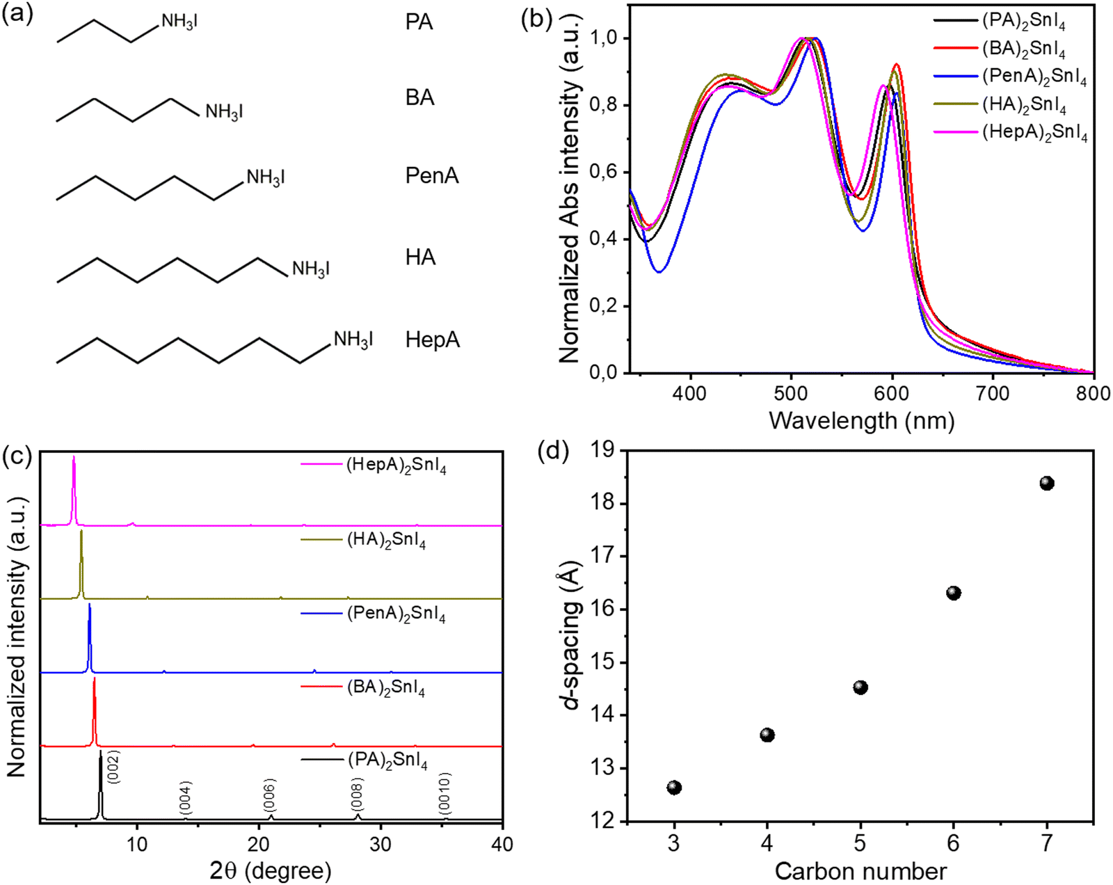 | ||
| Fig. 1 (a) Chemical structures of PA, BA, PenA, HA, and HepA organic spacers. (b) UV-Vis absorption spectra and (c) XRD patterns of 2D tin halide perovskite films based on different organic cations. (d) Relationship between different cations (carbon numbers) and d-spacing values of (002) diffraction peaks. | ||
The impact of the organic spacers on the crystal structure of the 2D tin halide perovskites is studied by X-ray diffraction (XRD). As shown in Fig. 1(c), the XRD diffractograms of all thin films show typical (00l) (where l = 2, 4, 6, 8, and 10) diffraction peaks of these 2D perovskite thin films with the facet signals of (002) at 7°, 6.49°, 6.09°, 5.42°, and 4.81°, respectively.25 Based on Bragg's law, the corresponding d-spacing values between the (002) planes of (PA)2SnI4, (BA)2SnI4, (PenA)2SnI4, (HA)2SnI4, and (HepA)2SnI4 are calculated to be 12.6 Å, 13.6 Å, 14.5 Å, 16.3 Å and 18.4 Å, respectively (Fig. 1(d)). It should be pointed out that the interlayer distances show an almost linear trend with the length of intercalating cations in the 2D perovskites. We also find that the longer cations lead to broader (00l) diffraction peaks. The (002) diffraction peaks of these samples have a full width at half maximum (FWHM) of 0.15°, 0.16°, 0.16°, 0.19°, and 0.21°, respectively. This indicates a lower crystallinity of the perovskites with spacer cations of longer chains due to their flexible nature and lower lattice rigidity.26
The surface morphologies of these perovskite films obtained by different casting parameters (concentration and solvent) are examined by atomic force microscopy (AFM) and the corresponding height images are presented in Fig. 2. The (PA)2SnI4 and (BA)2SnI4 films cast from 0.1 M dimethylformamide (DMF) solution show poor morphologies with pinholes and low film coverage compared with the other three films (Fig. 2(a)–(e)). Specifically, the (PA)2SnI4 film exhibits uniform 2 μm large grains with a root mean square (RMS) of 9 nm for the surface roughness. The grain size of the (BA)2SnI4 film is significantly increased to more than 6 μm. Nevertheless, the film shows large pinholes and a high RMS value of 17 nm. The rough surface between the perovskite semiconducting film and electrode can retard the charge injection, which is detrimental for the device performance.27 In contrast, (PenA)2SnI4, (HA)2SnI4 and (HepA)2SnI4 films with longer organic ligands reveal an improved continuity and flatter surface with RMS less than 5 nm (Fig. S1, ESI†). However, their corresponding grain size significantly reduced to below 1 μm.
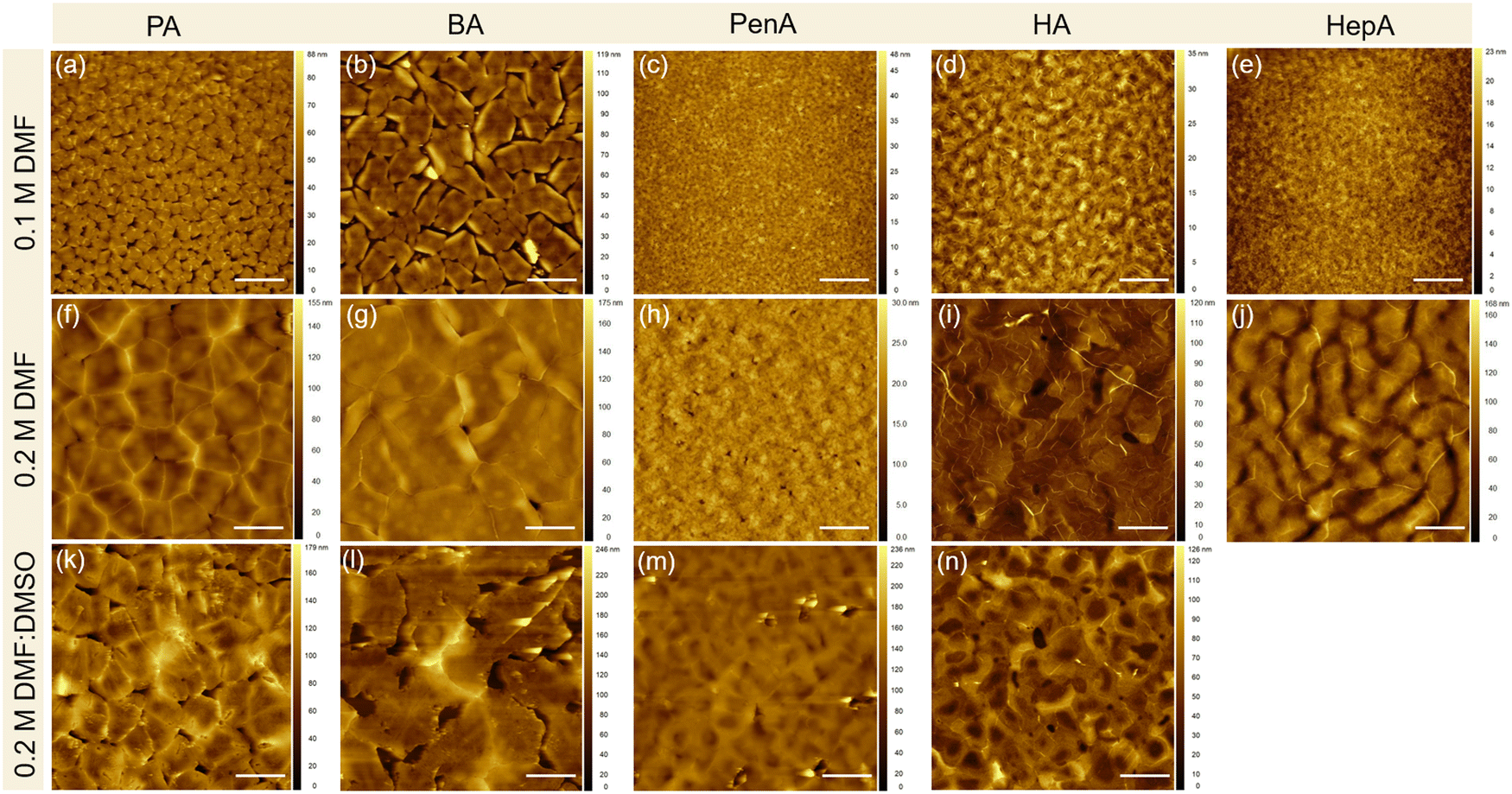 | ||
| Fig. 2 AFM height images of 2D tin halide perovskite films with different spacers PA, BA, PenA, HexA, and HepA obtained under the processing conditions of (a)–(e) 0.1 M, DMF; (f)–(j) 0.2 M, DMF; (k)–(n) 0.2 M, DMF:DMSO, respectively. Scale bar: 10 μm. | ||
To fine tune the morphology, the concentration of the precursor solution is adjusted from 0.1 M to 0.2 M, which has been proven as an effective method in the literature.28Fig. 2(f)–(j) show the surface morphologies for the 2D tin halide perovskite thin films with various spacer cations. All films reveal satisfactory homogenous surface topography with increased grain size. The enhanced morphologies are expected to favor the transistor performance by reducing charge trapping at grain boundaries. We carried out scanning electron microscopy (SEM), photoluminescence (PL), and time-resolved PL (TRPL) of the optimized perovskite thin films with a perovskite precursor concentration of 0.2 M in the pure DMF solvent. Fig. S2 (ESI†) displays the top-view SEM image of these perovskite films that exhibit homogeneously distributed grains without visible pinholes. This is in line with the observation of the film morphologies by AFM. Additionally, these films show one strong photoluminescence (PL) peak at around 615 nm indicating similar bandgaps for all samples, as shown in Fig. S3a (ESI†). Furthermore, TRPL spectroscopy was employed to assess the quality of these perovskites (Fig. S3b, ESI†). Longer PL lifetime of (HA)2SnI4 is observed compared to the other thin films confirming less defects in the corresponding film.29,30
To further improve the morphology formation and the crystallinity of the perovskite films prepared at a higher concentration of 0.2 M, dimethyl sulfoxide (DMSO) is added to the DMF solution. Pure DMF has relatively low Gutmann donor number of 26.6 kcal mol−1 compared to DMSO with 29.8 kcal mol−1.31 A solvent with a high Gutmann number strongly coordinates with the inorganic precursor [SnI6]4− octahedral sheets and suppresses the formation of molecular clusters. The strong coordination ability of DMSO is expected to reduce the nucleation rate of perovskite crystals due to the presence of pre-nucleation.13 The boiling point is another key parameter to determine the evaporation rate of the solvent and should be considered when mixing with DFM. It is generally believed that polar DMSO with high boiling point of 189 °C is less volatile and can readily remain in the perovskite film even after thermal annealing.32 The residual solvent in the film can decrease the crystallinity leading to reduced film quality. Therefore, in our case we kept the mixed ratio of DMF![[thin space (1/6-em)]](https://www.rsc.org/images/entities/char_2009.gif) :DMSO at 1:1. Fig. 2(k)–(n) show the four perovskite films based on the cations of PA, BA, PenA, and HA. All films possess a relatively high surface roughness with RMS values of 21, 34, 18, and 16 nm, respectively. Additionally, these films exhibit larger grain size but with randomly distributed pinholes. When the longest alkyl chain HepA is used, a striped film surface is observed, as shown in Fig. S4 (ESI†). The stripe-like morphology is possibly attributed to the high viscosity of the precursor solution during spin-coating.33 The above results illustrate that the film morphology can be easily tuned by the processing parameters for applications in FET devices. It is worth noting that the correlation between the chosen spacer and the resulting crystal nucleation and thin film morphology is still not well understood. In our case, we generally observed decreased surface roughness with longer spacers under various processing parameters. Nevertheless, there is no clear trend for grain size distribution of these five thin films. This should be further investigated in future.
:DMSO at 1:1. Fig. 2(k)–(n) show the four perovskite films based on the cations of PA, BA, PenA, and HA. All films possess a relatively high surface roughness with RMS values of 21, 34, 18, and 16 nm, respectively. Additionally, these films exhibit larger grain size but with randomly distributed pinholes. When the longest alkyl chain HepA is used, a striped film surface is observed, as shown in Fig. S4 (ESI†). The stripe-like morphology is possibly attributed to the high viscosity of the precursor solution during spin-coating.33 The above results illustrate that the film morphology can be easily tuned by the processing parameters for applications in FET devices. It is worth noting that the correlation between the chosen spacer and the resulting crystal nucleation and thin film morphology is still not well understood. In our case, we generally observed decreased surface roughness with longer spacers under various processing parameters. Nevertheless, there is no clear trend for grain size distribution of these five thin films. This should be further investigated in future.
To explore how the molecular organization of these 2D tin halide perovskites is affected by the spacers and processing conditions, grazing incidence wide-angle X-ray scattering (GIWAXS) measurements are performed and the results are presented in Fig. 3. The GIWAXS patterns of the films show a specific set of (00l) planes along the out-of-plane (qz) direction, indicating a layered perovskite structure and parallel arrangement of the inorganic [SnI6]4− sheets to the substrate, which is beneficial for charge carrier transport in the transistor channel.34 The corresponding intensity profiles along the qz axis are plotted in Fig. S5 (ESI†). The interlayer distances are calculated to be 12.7 Å, 13.9 Å, 15 Å, 16.8 Å, and 18.9 Å for PA, BA, PenA, HA, and HepA-based perovskite thin films, respectively, which is consistent with the XRD results. For the shortest alkyl chain PA-based perovskite, films prepared under three processing conditions show distinct diffraction peaks indicating high crystallinity. Debye–Scherrer rings with relatively uniform azimuthal intensities for the (PA)2SnI4 film indicate a random crystallographic orientation and certain structural misalignment towards the surface (Fig. 3(a), (f) and (k)).35 A similar behavior is observed for the (BA)2SnI4 film (Fig. 3(b), (g) and (l)). The dominant spot-like scattering patterns are superimposed with sparse arc-like signals, indicating the randomly oriented components.36 Interestingly, when the chain length of the spacer cation is further increased to PenA, HA, and HepA, the ring-like scattering signals gradually disappear and broad high-intensity reflections emerge indicating a reduced crystallinity, but enhanced arrangement towards the surface. Additionally, the in-plane (010) and (020) reflection peaks are attributed to Sn–I and I–Sn–I bonds. With an increase in the concentration to 0.2 M with pure DMF, a strong (020) reflection is observed for the HexA-based perovskites with longer alkyl cations (Fig. S6, ESI†). However, for films obtained from the mixed solvents DMF:DMSO, only the (HA)2SnI4 film shows a distinct intensity for the (020) facet. The diffraction pattern of the (020) plane with high intensity indicates the formation of well aligned perovskite octahedral building blocks. Since the charge transport is confined in the inorganic [SnI6]4− frameworks of the 2D layered perovskite, we infer that organic cations with a long chain length such as HA are more favorable for enhancing the preferred orientation and charge carrier transport in 2D tin halide perovskite films.37
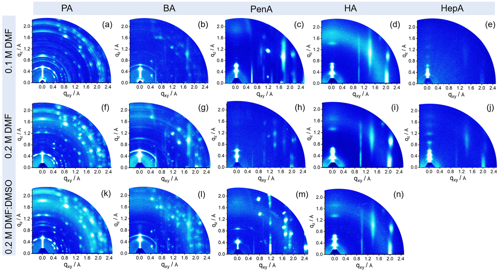 | ||
| Fig. 3 GIWAXS patterns of 2D tin halide perovskite films based on different organic spacers PA, BA, PenA, HA, and HepA with the processing parameters of (a)–(e) 0.1 M, DMF; (f)–(j) 0.2 M, DMF; (k)–(n) 0.2 M, DMF:DMSO, respectively. | ||
To unveil the local charge transport in these five 2D tin halide perovskite films, we employed optical pump–THz probe spectroscopy to characterize their photoconductivities. Due to the transient nature of the THz pulse (∼1–2 ps duration), the THz probe reports the local, intrinsic in-plane charge transport properties (e.g. charge carrier mobility) in a spatial range of ∼10 nm. As sketched in Fig. 4(a), a beyond-band gap excitation generates free charge carriers. The conductivity of these photogenerated charge carriers, i.e. photoconductivity Δσ, is directly probed by the THz pulse in the transmission geometry. The Δσ is related to the relative attenuation of the THz peak field (ΔE = EP − E0, with EP and E0 representing the transmitted THz peak field with and without excitation) following 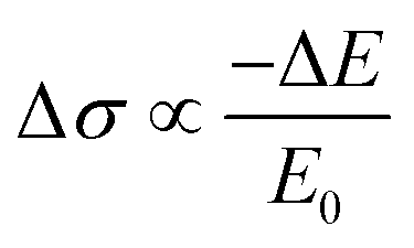 based on the thin-film approximation.38,39Fig. 4(b) compares the photoconductivity dynamics of the five samples with varied interlayer spacer length (C3–C7). In principle, Δσ can be expressed as Δσ = ΔN × e × μ, with e and μ representing the elementary charge and charge carrier mobility. The free charge carrier density ΔN can be further related to the absorbed photon density Nabs and the photon-to-free-carrier quantum efficiency ϕ (0 ≤ ϕ ≤ 1) following ΔN = Nabs × ϕ. To better compare the intrinsic charge transport, the free carrier generation quantum efficiency and mobility
  are compared and the peak values are summarized in Fig. 4(c). With an increase in the interlayer spacer length, for a given ϕ, the charge carrier mobility monotonically increases (by ∼60% by comparing C7 to C3). ϕ is expected to decrease with an increase in the spacer length, as the efficiency of the interlayer electron–hole separation drops, which is one of the main free carrier generation schemes in nanoscale materials. The mobility enhancement observed here by increasing the spacer length is therefore likely underestimated.
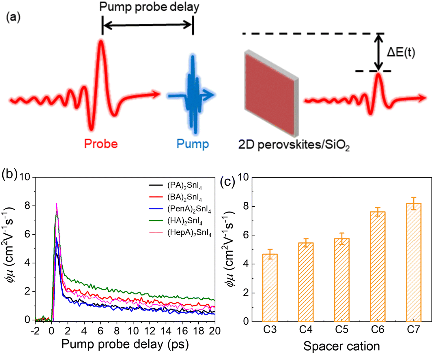 | ||
| Fig. 4 (a) Photoconductivity dynamics by optical pump–THz probe (OPTP) spectroscopy. (b) Comparison of the mobility and free-carrier generation quantum efficiency (ϕμ) for the five perovskites. (c) Charge carrier mobility (peak values in a) as a function of the chain length of the spacer cation. | ||
To further unveil the effect of film morphology and molecular organization on long-range charge carrier transport in FETs for the above discussed five 2D perovskites, bottom-gate top-contact devices were fabricated as shown in Fig. 5(a). The electrical characteristics of these devices were measured in a vacuum chamber at different temperatures from 100 K to 295 K. The transfer characteristics were recorded at Vds = −60 V with Vg scans from +60 V to −60 V. The corresponding mobilities are summarized in Fig. 5(b). All device parameters are extracted from the saturation region of the transfer curves in the forward direction. At lower casting concentration of 0.1 M, as shown in Fig. S7 (ESI†), devices based on (PA)2SnI4 and (BA)2SnI4 yield very small channel currents at room temperature, which are similar to the leakage current Ig of 10−9 A. The large pinholes in the films probably result in limited charge transport in the lateral direction and finally in poor device parameters.40 When the alkyl chain length increases, the devices show a clear typical p-channel behavior. Despite the improved transfer characteristics, the devices exhibit a low performance with the highest mobility (μ) of 2.5 × 10⁻³ cm2 V−1 s−1 obtained for (HA)2SnI4. We performed UPS measurements to study the electronic structure of these five 2D lead-free perovskite semiconductors (Fig. S8, ESI†). The valence-band maximum (VBM) values are determined to be −5.40, −5.52, −5.68, −5.53, and −5.64 eV for (PA)2SnI4, (BA)2SnI4, (PenA)2SnI4, (HA)2SnI4 and (HepA)2SnI4, respectively. The corresponding conduction-band minimum (CBM) values of these perovskite films are −3.44, 3.57, −3.71, −3.56, and −3.67 eV based on the optical band gap, as shown in Fig. S9 (ESI†). For the observed hole injection barriers at the perovskite–electrode contacts, through optimization of the contact resistance and the choice of optimized functional layer materials and electrode metals, some improvements in the field-effect mobility could be achieved in future.41
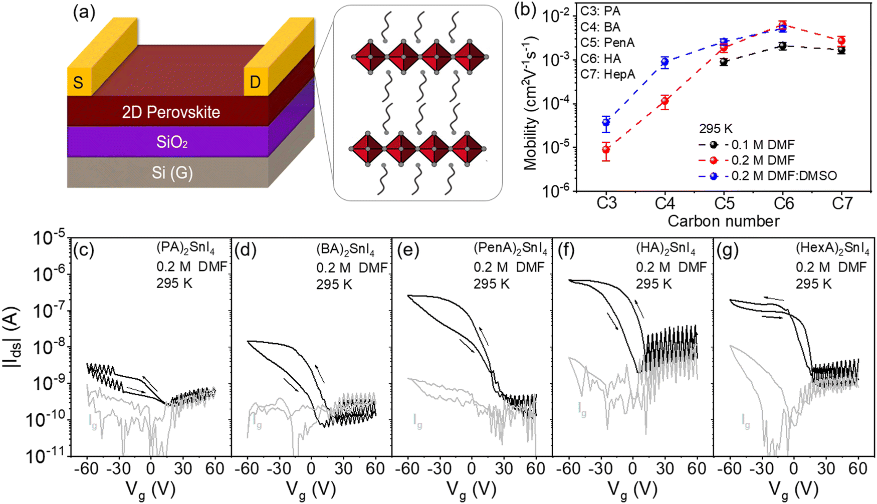 | ||
| Fig. 5 (a) Schematic diagram of a bottom-gate top-contact FET device. (b) Statistic summary of charge carrier mobilities as a function of carbon number of the spacer cation for different film casting parameters. Transfer characteristics of (c) (PA)2SnI4; (d) (BA)2SnI4; (e) (PenA)2SnI4; (f) (HA)2SnI4; and (g) (HepA)2SnI4 for the precursor concentration of 0.2 M and solvent DMF. Arrows indicate the direction of the sweeps. | ||
As the concentration is increased to 0.2 M, all devices demonstrate an enhanced performance, which is likely to account for the improved film morphologies and molecular organization. Particularly, the increased grain size is beneficial for suppressing ion migration and enhancing charge carrier transport since grain boundaries are considered as defects in the film, as confirmed in our previous work.19 There is no direct relationship between the film roughness and electrical properties of the FET devices since the perovskite films processed from 0.1 M and 0.2 M concentrations exhibit similar surface roughness. The device based on PA with the shortest chain length still reveals an extremely low drain current possibly due to the pronounced crystallite misalignment in the (PA)2SnI4 film and the low intrinsic mobility, as confirmed by THz spectroscopy. The (HA)2SnI4 based perovskite FET reveals the highest μ of 8 × 10⁻³ cm2 V−1 s−1 among all the devices and corresponds well with the highest surface orientation of the inorganic [SnI6]4− sheets in the layered perovskite structure, demonstrating electrical parameters comparable to those of previously reported perovskite 2D lead-free perovskite FETs (Table S1, ESI†). We then investigated the champion device based on the (HA)2SnI4 semiconducting layer in the linear region at Vds of −5 V. As shown in Fig. S10 (ESI†), the corresponding device exhibits a reduced field-effect mobility of 2.1 × 10⁻³ cm2 V−1 s−1 compared to the device measured in the saturation region. The transfer curves also exhibit a large dual-sweep hysteresis, which is expected when ions migrate and accumulate at the semiconductor/dielectric interface under gate bias. These concentrated mobile ions screen the applied gate electric field and reduce the concentration of hole charge carriers in the device.42 We have also investigated the bias stress stability for the (HA)2SnI4 FETs. Fig. S11 (ESI†) shows the change in the source–drain current under a constant bias of Vg = Vds = −60 V for 500 s. The normalized source–drain current (Ids(t)/Ids(0)) of the corresponding device degrades significantly, which could be attributed to defects and ion migration in the perovskite thin film.
We further discuss and compare the THz and FET studies on quantifying the charge carrier mobility. As mentioned, the THz spectroscopy probes the charge transport in the spatial scale of tenths of nanometers. In contrast, in FET devices, charge carriers drift over tenths of micrometers along the applied electric field in the channel. This rationalizes orders of magnitude difference in the mobility as THz spectroscopy sheds light on local charge transport (within a single crystal domain), while in FETs, the charge carriers percolate through multiple perovskite domains separated by boundaries from each other. In both studies, we observe that the charge carrier mobility rises on increasing the spacer length. However, the mobility enhancement scales differently. By changing the spacer length from C3 to C6 or C7, the long-range charge carrier mobility inferred from FETs boosts by ∼3 orders of magnitude. This is in sharp contrast to the moderate increase of ∼60% of the local charge carrier mobility determined by THz spectroscopy. These results indicate that the transport bottleneck in the FET lies in film morphology, rather than in the local crystal packing. Improving the preferential crystal orientation of the 2D layers by increasing the spacer length and enlarging the domain size by lowering the density of domain boundaries can presumably reduce the energy barrier and/or disorder and thus facilitate charge transport in the FET devices.
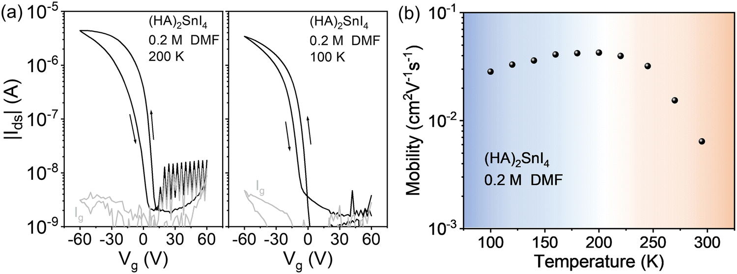
We then explore the low temperature device performance of the (HA)2SnI4 FET, which gives the best device performance at room temperature. Fig. 6(a) exhibits the corresponding transfer curves at two temperatures of 200 K and 100 K. Compared with the room temperature transfer characteristics, the device at low temperatures shows a more pronounced field-effect modulation. At 200 K, the FET mobility amounts to 4.2 × 10⁻² cm2 V−1 s−1, while at 100 K. the mobility is slightly lowered to 2.9 × 10⁻² cm2 V−1 s−1 with a significantly suppressed hysteresis. We defined the difference of Vg (ΔVhys) at |Ids| = 1 × 10⁻⁷ A, which is around halfway between the on and off states, under both forward and backward sweeping directions in the transfer characteristics to quantitively analyze the degree of hysteresis. The (HA)2SnI4 FET device shows ΔVhys of 20 V and 14 V at 295 K, and 200 K, respectively, which are substantially larger than the 8 V at 100 K. It is generally believed that the ion migration and interface traps induce the dual-sweep hysteresis in halide perovskite FETs.43 The mobile ion induced hysteresis is strongly dependent on the operation conditions and can be significantly suppressed by lowering the temperature.19 Therefore, the large hysteresis observed at room temperature mainly can be ascribed to the severe ion movement in the channel. In addition, the residual hysteresis at 100 K indicates the formation of interfacial traps between dielectric and semiconducting layers since ion movement is almost completely inhibited at such low temperature.20
 | ||
| Fig. 6 Low temperature transfer characteristics of the (HA)2SnI4-based FET device at (a) 200 and 100 K. (b) Corresponding temperature-dependent field-effect mobility from 100 K to 295 K. | ||
Fig. 6(b) shows the temperature-dependent mobility measurements of (HA)2SnI4 FETs from 100 K to 295 K. In the case of (HA)2SnI4, two mobility regimes in the whole temperature range are identified. In the first region, the field-effect mobility increases on rising the temperature from 100 K to around 200 K, which manifests a thermally activated transport mechanism. At the same time, a possible increase of the ion migration cannot be neglected as indicated by the larger hysteresis. When the temperature is further elevated from 200 K to 295 K, a negative coefficient of mobility is observed. In general, the temperature dependence of charge-carrier mobility in the semiconductors can be analyzed by fitting a typical power law behavior μ ∝ T−γ, where γ reflects the magnitude of charge scattering.42 Interestingly, the mobility in the high temperature regime of 200 K to 295 K shows a large γ value of 3.1, which is comparable to the ones observed in MAPbI3 FETs, indicating that the charge carrier transport in this regime is dominated by ion migration.44 Iodine vacancies are generally considered as dominating ionic defects in 2D Sn-based perovskites due to their low formation energy.43 At high temperature, mobile ions move in the in-plane direction in the transistor and accumulate at the source/drain electrodes driven by the external applied Vds. The accumulation of ions screens the electric field generated by Vds, which slows down charge carrier transport as confirmed by the higher maximum channel current at 200 K compared to the device at 295 K.
The crystallographic structure evolutions during temperature variation complicates the operation mechanism of perovskite based electronic devices by changing their charge transport properties with different crystal phases. Therefore, we employed the temperature-dependent XRD measurement to reveal the influence of temperature on the crystal structure and the field-effect mobility of 2D (HA)2SnI4 perovskites. For each temperature, the sample was slowly cooled down and kept at this level until temperature stabilization. This controlled procedure ensured high consistency and homogenous temperature distribution over the sample. As shown in Fig. 7(a) (left panel), all the diffraction patterns of the (HA)2SnI4 perovskite thin film exhibit similar behavior over the entire temperature range from 100 to 295 K, indicating that no definite degradation occurs during the heating process. Meanwhile, the diffraction peaks show a slight shift toward a lower angle (right panel in Fig. 7(a)). This leads to a moderate increase of the interlayer distance along with the (002) facet, as shown in Fig. 7(b). However, an abrupt change of d002 near 160–170 K was observed. One possible explanation is the phase transition. Previous studies reveal that 2D perovskites with linear aliphatic cations (CnH2n+1NH3)2MX4 can exhibit structural phase transitions at low temperatures, which are associated with changes in ordering and hydrogen bonding of the organic cations.45,46 Nevertheless, it should be pointed out that the corresponding interlayer distance shows a very small variation of only 0.1 Å, which may be the reason why it is not reflected in the temperature-dependent charge mobility measurement of the corresponding FET devices. The above discussion suggests that the effect of phase transition on the corresponding device performance of (HA)2SnI4 perovskite FETs can be excluded with the temperature.
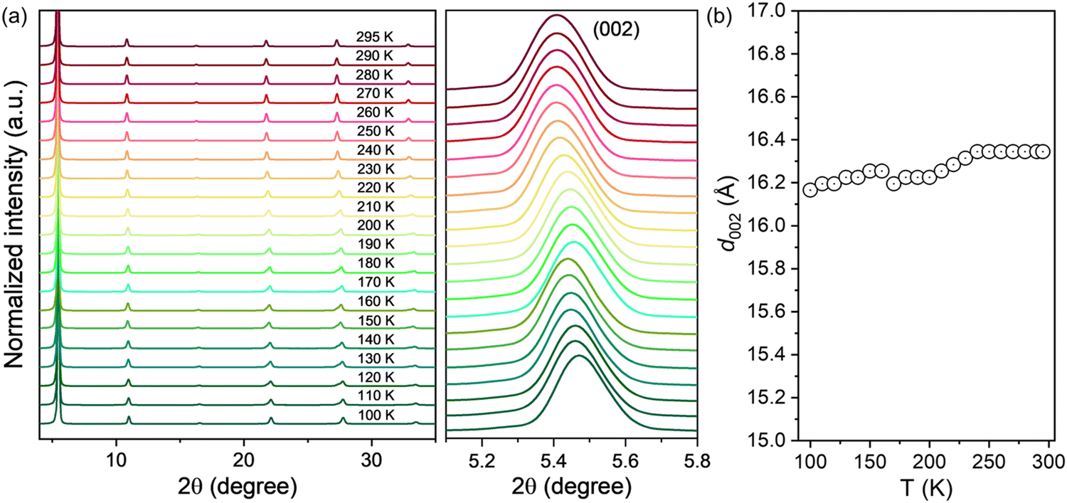 | ||
| Fig. 7 (a) XRD patterns as a function of the temperature from 100 to 295 K for the (HA)2SnI4-based perovskite film and the XRD peak of the (002) facet; (b) the interlayer distance as a function of the temperature for the peak (002). | ||
In the last step, to verify the effects of the co-solvent DMSO on device parameters, FETs based on (PA)2SnI4, (BA)2SnI4, (PenA)2SnI4, and (HA)2SnI4 were fabricated and the results are shown in Fig. 8. Compared to the devices prepared from pure DMF, the FETs obtained from the mixed DMF:DMSO solvent reveal overall improved electrical parameters with significantly reduced dual-sweeping hysteresis and channel current. For example, the calculated ΔVhys values of (PenA)2SnI4, and (HA)2SnI4 FETs at |Ids| = 1 × 10⁻⁷ A are only 4 V and 3 V, respectively. Similar behavior is observed for devices of the other perovskites. The hysteresis of perovskite FETs is generally assigned to the migration of ionic defects.39 The lower hysteresis can be explained by the strong coordination ability between DMSO and SnI2 precursor by forming an intermediate phase during the crystallization process, which can suppress the generation of ionic defects. The above results demonstrate that solvent engineering can serve as an efficient strategy to improve the charge carrier transport in 2D tin halide perovskites.
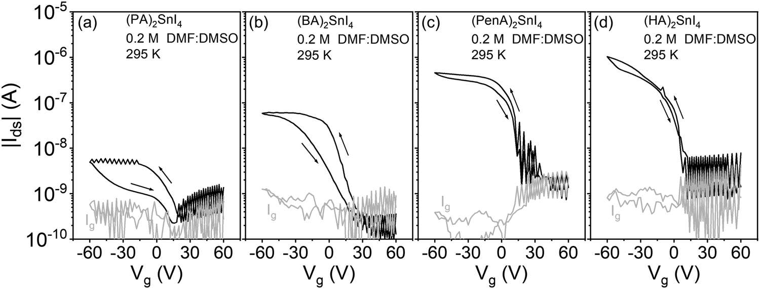 | ||
| Fig. 8 Transfer characteristics of (a) (PA)2SnI4; (b) (BA)2SnI4; (c) (PenA)2SnI4; and (d) (HA)2SnI4; for the precursor concentration of 0.2 M and mixed solvent DMF:DMSO. Arrows indicate the direction of the sweeps. | ||
Conclusion
We demonstrated the effect of organic spacers on film morphology, crystallinity, and charge carrier transport in 2D tin halide perovskites by incorporating a series of linear alkyl ammonium organic spacers of different side chain lengths. It is found that the chain length of the spacer cation and the film processing parameters significantly influence the organization of organic cations and film morphology, which in turn affect the charge transport properties. The short allylic cation-based perovskites retain random crystal orientation. By contrast, prolonging the carbon number leads to preferential formation of oriented structures. THz photo-conductivity measurements demonstrate exceptional charge carrier transport with local mobility of over 8 cm2 V−1 s−1 for perovskites with longer linear cations. Additionally, 2D layered tin halide perovskites exhibited higher in-plane macroscopic charge mobility with increasing organic chain length to HA. Therefore, incorporation of longer-chain spacers is an effective strategy to enhance the charge transport properties in 2D layered tin halide perovskites. Additionally, temperature-dependent charge transport measurements on the optimized (HA)2SnI4 FET revealed a transition from a negative mobility coefficient with dominated ion migration to a thermally activated regime at around 200 K. Taken together, this work offers new insights into the effect of chemical nature of organic cations on the electronic properties of 2D perovskites at the molecular level.Experimental section
Materials
All chemical reagents and solvents were used without further purification. Organic cations were ordered from Xi’an Polymer Light Technology Corp. Tin(II) iodide (SnI2, 99.999%), N,N-dimethylformamide (DMF, anhydrous, 99.8%), and dimethyl sulfoxide (DMSO, anhydrous, ≥99.9%) were purchased from Sigma-Aldrich. Heavily doped silicon wafers were ordered from Ossila.Device fabrication and measurement
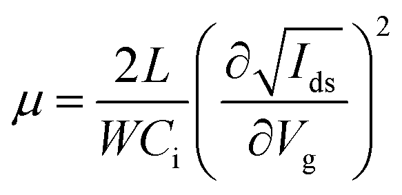
The bottom-gate top-contact configuration was employed for the FET devices. The heavily p-doped bare Si/SiO2 wafers (1.5 × 2 cm) were used as the substrates and cleaned in an ultrasonic bath with deionized water, acetone, and isopropyl alcohol and then blown dry with N2. The SiO2 layer with a thickness of 300 nm was adopted as a dielectric layer. The cleaned substrates were treated by UV light for 20 min and then transferred into a glove box for perovskite film deposition. The 2D perovskite precursor solution with concentrations of 0.1 and 0.2 M was prepared in a stoichiometric ratio of organic spacers and SnI2 (2:1) in DMF or DFM:DMSO (v/v 1:1) solvent. The solution was stirred overnight at 60 °C in a glove box and cooled to room temperature before use. The as-prepared fresh precursor solution was spin-coated with a 0.2 μm PTFE filter at 4000 rpm for 60 s and annealed at 100 °C for 10 min. Finally, the source and drain electrodes were deposited with a thickness of 80 nm by gold thermal evaporation through a shadow mask to construct 80 × 1000 μm (length × width) transistor channels. The device characterization was performed using a semiconductor parameter analyzer (Keithley 4200-SCS) in a low-temperature probe station. The transfer characteristics were collected in pulse mode, and the output characteristics were measured in continuous mode. In the pulse mode, Vg was applied over a short impulse of 1 s. The temperature-dependent measurements were performed using a Desert Cryogenics low-temperature probe station. Mobility values of FETs are extracted with the following equation:where L, W, and Ci are the channel length and width and the unit capacitance of the oxide dielectric, respectively.
Characterization
Thin film absorption spectra were recorded on an Agilent UV-Vis-NIR Cary-5000 spectrometer in transmission mode. Data were collected from 380–800 nm using a dwell time of 0.1 s. During all measurements, the samples were kept in air and at room temperature. The thin film morphology was characterized using a Bruker Dimension Icon FS AFM in tapping mode at room temperature. The root mean square (RMS) roughness values were extracted from an image of 50 μm × 50 μm. Top-view scanning electron microscopy (SEM) images of the perovskite thin films were taken using a Zeiss LEO1530 VP SEM with an in-lens detector and an aperture size of 20 μm. The perovskite films were deposited on silicon substrates. The steady PL spectra were measured using a steady-state fluorescence spectrometer (Edinburgh Instruments, FLS980) with an excitation wavelength of 400 nm, while the PL decay curves were recorded by using the kinetic model of FLS980 with a 400 nm nanosecond pulsed diode laser. Grazing incidence wide-angle X-ray scattering (GIWAXS) measurements were performed at the Dortmund Electron Accelerator (DELTA) Synchrotron Facility (Dortmund, Germany), beamline BL09. The photon energy was set to 10 keV (λ = 1.54 Å). The incident angle (αi) of the X-ray beam was adjusted individually for each sample in the range of 0.08°–0.12°. The scattered intensity was recorded by a 2D image plate (MAR345, marXperts GmbH, Norderstedt, Germany). The exposure time was 180 s. The q-range (q = 4 × π × sinθ × λ−1) was calibrated using silver behenate standard. The data were processed and analyzed using Datasqueeze (University of Pennsylvania, Philadelphia, PA, USA) and OriginPro (OriginLab Corporation, Northampton, MA, USA). All measurements were performed under vacuum (∼1 mbar) to reduce air scattering and beam damage to the sample and the degradation of perovskite materials. The film XRD patterns were recorded in the 2θ between 3° and 40°, with a step of 0.01° and a speed of 5 degrees per minute, using a Rigaku D/MAX 2600 V with Cu Kα (λ = 1.5406 Å) radiation. The interlayer distance was calculated using Bragg's law: 2dsinθ = nλ, where θ = 5.66° and n = 2, respectively. For UPS characterization, to avoid any charging during the measurement, Si wafers were coated with Cr/Au (2 nm/50 nm) as the conductive layer by thermal evaporation. Then samples were transferred into the UPS chamber and measurements were carried out at a base pressure of 10−8 torr. Photoelectron emission was collected at 0° from the surface normal of the samples. The spectra were taken in three different spots to confirm producibility of the spectra and irradiation exposure time was kept under one minute.
Optical pump–THz probe (OPTP) spectroscopy
The THz setup is driven by a commercial, regenerative amplified, mode-locked femtosecond laser. The 1 kHz Ti:sapphire regenerative amplifier laser produces 1.55 eV near-infrared pulse (800 nm, 50 fs). The THz setup is purged by dry nitrogen in a closed box. THz pulses are generated by optical rectification in a 1 mm thick ZnTe crystal. The THz electrical field is probed in a second ZnTe crystal in the time domain by the electro-optic effect, by varying the time delay between THz and sampling pulse with an optical delay stage. For the OPTP measurements, the excitation light is 400 nm, which is produced by second harmonic generation based on 800 nm light using a beta barium borate (BBO) crystal. The OPTP signals are measured at the THz peak. A delay stage is used to vary the time delay between the pump and probe beam.Author contributions
T. M., and W. P. supervised the project; S. L. W. conceived the idea and designed the experiment; S. L. W. and S. K. performed the experiment and general measurement; L. G. conducted the THz spectroscopy measurement and analyzed the data with support from H. I. W.; Z. T. L. participated in GIWAXS measurement and data analysis under the supervision of T. M.; Z. W. Z. carried out the photoluminescence spectra measurement; S. L. W. composed the manuscript with input from all co-authors; M. B. and P. B. provided expertise and coordinated the work. All authors discussed the results and contributed to this work.Conflicts of interest
There are no conflicts to declare.Acknowledgements
S. Wang thanks the China Scholarship Council (CSC.201906890035) for financial support. T. Marszalek acknowledges the Foundation for Polish Science financed by the European Union under the European Regional Development Fund (POIR.04.04.00-00-3ED8/17). W. Pisula acknowledges the National Science Centre, Poland, through the grant UMO-2019/33/B/ST3/1550. The authors acknowledge Beamline 9 of the DELTA electron storage ring in Dortmund for providing synchrotron radiation and technical support for GIWAXS measurements. The authors also acknowledge Prof. Dr Ni Zhao from The Chinese University of Hong Kong for providing support for UPS measurements and Gunnar Glaßer from Max Planck Institute for Polymer Research for SEM surface studies. Open Access funding provided by the Max Planck Society.References
- C. R. Kagan, D. B. Mitzi and C. D. Dimitrakopoulos, Science, 1999, 286(5441), 945–947 CrossRef CAS PubMed.
- Y. Li, Z. Shi, W. Liang, J. Ma, X. Chen, D. Wu and X. Fang, Mater. Horiz., 2021, 8(5), 1367–1389 RSC.
- W. Xu, H. Cho, Y. H. Kim, Y. T. Kim, C. Wolf, C. G. Park and T. W. Lee, Organometal halide perovskite artificial synapses, Adv. Mater., 2016, 28(28), 5916–5922 CrossRef CAS PubMed.
- H. Zheng, H. Xu, F. Zheng, G. Liu, X. Xu, S. Xu and X. Pan, ChemSusChem, 2020, 13(1), 252–259 CrossRef CAS PubMed.
- J. Hu, L. Yan and W. You, Adv. Mater., 2018, 30(48), 1802041 CrossRef PubMed.
- A. J. Magdaleno, M. Seitz, M. Frising, A. H. de la Cruz, A. I. Fernández-Domínguez and F. Prins, Mater. Horiz., 2021, 8(2), 639–644 RSC.
- Y. Chen, Y. Sun, J. Peng, J. Tang, K. Zheng and Z. Liang, Adv. Mater., 2018, 30(2), 1703487 CrossRef PubMed.
- Y. Zheng, T. Niu, X. Ran, J. Qiu, B. Li, Y. Xia and W. Huang, J. Mater. Chem. A, 2019, 7(23), 13860–13872 RSC.
- H. Zheng, G. Liu, L. Zhu, J. Ye, X. Zhang, A. Alsaedi and S. Dai, Adv. Energy Mater., 2018, 8(21), 1800051 CrossRef.
- X. Jiang, J. Zhang, S. Ahmad, D. Tu, X. Liu, G. Jia and C. Li, Nano Energy, 2020, 75, 104892 CrossRef CAS.
- Y. Lin, Y. Bai, Y. Fang, Q. Wang, Y. Deng and J. Huang, ACS Energy Lett., 2017, 2(7), 1571–1572 CrossRef CAS.
- A. Liu, H. Zhu, S. Bai, Y. Reo, T. Zou, M. G. Kim and Y. Y. Noh, High-performance inorganic metal halide perovskite transistors, Nat. Electron., 2022, 5(2), 78–83 CrossRef CAS.
- X. Qiu, J. Xia, Y. Liu, P. A. Chen, L. Huang, H. Wei and Y. Hu, Ambient-Stable 2D Dion–Jacobson Phase Tin Halide Perovskite Field-Effect Transistors with Mobility over 1.6 cm2 V−1 s−1, Adv. Mater., 2023, 2305648 CrossRef CAS PubMed.
- F. Lédée, P. Audebert, G. Trippé-Allard, L. Galmiche, D. Garrot, J. Marrot and C. Quarti, Mater. Horiz., 2021, 8(5), 1547–1560 RSC.
- B. Kim and S. I. Seok, Energy Environ. Sci., 2020, 13(3), 805–820 RSC.
- X. Li, J. M. Hoffman and M. G. Kanatzidis, Chem. Rev., 2021, 121(4), 2230–2291 CrossRef CAS PubMed.
- T. Matsushima, S. Hwang, A. S. Sandanayaka, C. Qin, S. Terakawa, T. Fujihara and C. Adachi, Adv. Mater., 2016, 28(46), 10275–10281 CrossRef CAS PubMed.
- A. Liang, Y. Gao, R. Asadpour, Z. Wei, B. P. Finkenauer, L. Jin and L. Dou, J. Am. Chem. Soc., 2021, 143(37), 15215–15223 CrossRef CAS PubMed.
- S. Wang, S. Frisch, H. Zhang, O. Yildiz, M. Mandal, N. Ugur and T. Marszalek, Mater. Horiz., 2022, 9(10), 2633–2643 RSC.
- S. Wang, K. Bidinakis, C. Haese, F. H. Hasenburg, O. Yildiz, Z. Ling and T. Marszalek, Small, 2023, 2207426 CrossRef CAS PubMed.
- Y. Chen, Y. Sun, J. Peng, W. Zhang, X. Su, K. Zheng and Z. Liang, Adv. Energy Mater., 2017, 7(18), 1700162 CrossRef.
- R. Dong, C. Lan, X. Xu, X. Liang, X. Hu, D. Li and J. C. Ho, ACS Appl. Mater. Interfaces, 2018, 10(22), 19019–19026 CrossRef CAS PubMed.
- Z. Wang, F. Wang, B. Zhao, S. Qu, T. Hayat, A. Alsaedi and Z. A. Tan, J. Phys. Chem. Lett., 2020, 11(3), 1120–1127 CrossRef CAS PubMed.
- A. L. Alvarado-Leaños, D. Cortecchia, C. N. Saggau, S. Martani, G. Folpini, E. Feltri and A. Petrozza, ACS Nano, 2022, 16(12), 20671–20679 CrossRef PubMed.
- W. L. Tan and C. R. McNeill, Appl. Phys. Rev., 2022, 9(2), 021310 CAS.
- K. J. Kwak, J. H. Baek, D. E. Lee, I. H. Im, J. Kim, S. J. Kim and H. W. Jang, Ambient stable all inorganic CsCu2I3 artificial synapses for neurocomputing, Nano Lett., 2022, 22(14), 6010–6017 CrossRef CAS PubMed.
- Y. Zhang, M. Liu, G. E. Eperon, T. C. Leijtens, D. McMeekin, M. Saliba and H. J. Snaith, Mater. Horiz., 2015, 2(3), 315–322 RSC.
- Z. Li, S. P. Senanayak, L. Dai, G. Kusch, R. Shivanna, Y. Zhang and R. L. Hoye, Adv. Funct. Mater., 2021, 31(49), 2104981 CrossRef CAS.
- J. Gong, H. Wei, J. Liu, L. Sun, Z. Xu, H. Huang and W. Xu, An artificial visual nerve for mimicking pupil reflex, Matter, 2022, 5(5), 1578–1589 CrossRef.
- J. Liu, J. Gong, H. Wei, Y. Li, H. Wu, C. Jiang and W. Xu, A bioinspired flexible neuromuscular system based thermal-annealing-free perovskite with passivation, Nat. Commun., 2022, 13(1), 7427 CrossRef CAS PubMed.
- M. Abdel-Shakour, T. H. Chowdhury, K. Matsuishi, I. Bedja, Y. Moritomo and A. Islam, Sol. RRL, 2021, 5(1), 2000606 CrossRef CAS.
- E. Rezaee, W. Zhang and S. R. P. Silva, Solvent engineering as a vehicle for high quality thin films of perovskites and their device fabrication, Small, 2021, 17(25), 2008145 CrossRef CAS PubMed.
- G. Wu, T. Yang, X. Li, N. Ahmad, X. Zhang, S. Yue and Y. Zhang, Matter, 2021, 4(2), 582–599 CrossRef CAS.
- S. Shao, W. Talsma, M. Pitaro, J. Dong, S. Kahmann, A. J. Rommens and M. A. Loi, Adv. Funct. Mater., 2021, 31(11), 2008478 CrossRef CAS.
- D. Liang, C. Dong, L. Cai, Z. Su, J. Zang, C. Wang and B. Sun, Small, 2021, 17(33), 2100972 CrossRef CAS PubMed.
- H. Xu, Y. Jiang, T. He, S. Li, H. Wang, Y. Chen and J. Chen, Adv. Funct. Mater., 2019, 29(47), 1807696 CrossRef CAS.
- S. Yu, Y. Yan, M. Abdellah, T. Pullerits, K. Zheng and Z. Liang, Small, 2019, 15(49), 1905081 CrossRef CAS PubMed.
- M. C. Nuss and J. Orenstein, Terahertz time-domain spectroscopy, Millimeter and submillimeter wave spectroscopy of solids, 1998, pp. 7–50 Search PubMed.
- F. A. Hegmann, O. Oksana and D. G. Cooke, Probing organic semiconductors with terahertz pulses, Photophysics of Molecular Materials: From Single Molecules to Single Crystals, 2005, pp. 367–428 Search PubMed.
- H. Cao, Z. Zhang, M. Zhang, A. Gu, H. Yu, H. Ban and M. Wang, Mater. Today Phys., 2021, 21, 100513 CrossRef CAS.
- X. J. She, C. Chen, G. Divitini, B. Zhao, Y. Li, J. Wang and H. Sirringhaus, A solvent-based surface cleaning and passivation technique for suppressing ionic defects in high-mobility perovskite field-effect transistors, Nat. Electron., 2020, 3(11), 694–703 CrossRef CAS.
- S. P. Senanayak, B. Yang, T. H. Thomas, N. Giesbrecht, W. Huang, E. Gann and H. Sirringhaus, Sci. Adv., 2017, 3(1), e1601935 CrossRef PubMed.
- S. P. Senanayak, M. Abdi-Jalebi, V. S. Kamboj, R. Carey, R. Shivanna, T. Tian and H. Sirringhaus, Sci. Adv., 2020, 6(15), eaaz4948 CrossRef CAS PubMed.
- Y. Liu, P. A. Chen, X. Qiu, J. Guo, J. Xia, H. Wei and Y. Hu, iScience, 2022, 25(4), 104109 CrossRef CAS PubMed.
- D. G. Billing and A. Lemmerer, Acta Crystallogr., Sect. B: Struct. Sci., 2007, 63(5), 735–747 CrossRef CAS PubMed.
- Y. Takahashi, R. Obara, K. Nakagawa, M. Nakano, J. Y. Tokita and T. Inabe, Chem. Mater., 2007, 19(25), 6312–6316 CrossRef CAS.
Footnotes |
| † Electronic supplementary information (ESI) available. See DOI: https://doi.org/10.1039/d3mh01883k |
| ‡ These authors contributed equally to this work. |
| This journal is © The Royal Society of Chemistry 2024 |