
A high-dimensional in-sensor reservoir computing system with optoelectronic memristors for high-performance neuromorphic machine vision†
Yoon Ho
Jang‡
,
Joon-Kyu
Han‡
,
Sangik
Moon
,
Sung Keun
Shim
,
Janguk
Han
,
Sunwoo
Cheong
,
Soo Hyung
Lee
and
Cheol Seong
Hwang
 *
*
Department of Materials Science and Engineering and Inter-university Semiconductor Research Center, College of Engineering, Seoul National University, Seoul, 08826, Republic of Korea. E-mail: cheolsh@snu.ac.kr
First published on 15th November 2023
Abstract
In-sensor reservoir computing (RC) is a promising technology to reduce power consumption and training costs of machine vision systems by processing optical signals temporally. This study demonstrates a high-dimensional in-sensor RC system with optoelectronic memristors to enhance the performance of the in-sensor RC system. Because optoelectronic memristors can respond to both optical and electrical stimuli, optical and electrical masks are proposed to improve the dimensionality and performance of the in-sensor RC system. An optical mask is employed to regulate the wavelength of light, while an electrical mask is used to control the initial conductance of zinc oxide optoelectronic memristors. The distinct characteristics of these two masks contribute to the representation of various distinguishable reservoir states, making it possible to implement diverse reservoir configurations with minimal correlation and to increase the dimensionality of the in-sensor RC system. Using the high-dimensional in-sensor RC system, handwritten digits are successfully classified with an accuracy of 94.1%. Furthermore, human action pattern recognition is achieved with a high accuracy of 99.4%. These high accuracies are achieved with the use of a single-layer readout network, which can significantly reduce the network size and training costs.
New conceptsThe current in-sensor reservoir computing (RC) systems involve fused in-sensor computing with RC by utilizing volatile optoelectronic memristors as optical reservoirs. However, prior in-sensor RC approaches faced a challenge in creating higher-dimensional reservoirs, limiting the system's performance or versatility. This study introduces a novel method to address this limitation, capitalizing on the dual responsiveness of optoelectronic memristors to both optical and electrical stimuli. This method employs optical and electrical masks to diversify the reservoir state and enhance the reservoir dimensionality. Unlike conventional masking processes requiring intricate signal conversions, this technique enhances dimensionality efficiently in a controllable manner. Leveraging zinc oxide (ZnO) deposited using the atomic layer deposition technique, optoelectronic memristors were fabricated, which exhibited a large optoelectronic switching window of ∼103. Utilizing the fabricated ZnO optoelectronic memristor as a reservoir component, this system successfully classified MNIST handwritten digits (94.1%) and recognized human action patterns (99.4%). These results were achieved with a single-layer readout network, offering higher accuracy than previous studies. This study underscores the potential for novel computing hardware in materials research fields, marking a significant step toward the neuromorphic computing era. |
Introduction
A conventional machine vision system relies on optical sensors within the camera to collect analog visual data, which are converted to digital form through additional processing. However, this process requires analog-to-digital data conversion and extensive data transportation between the sensors and processors, resulting in significant energy consumption.1–3 Furthermore, conventional processors based on the von Neumann architecture demand significant data transmission between the separate memory and processing units, further exacerbating power consumption.4,5 Therefore, the conventional machine vision system has certain constraints for application in the Internet of Things and mobile devices, which require high energy efficiencies. Therefore, interest in in-sensor computing to address these issues is growing, inspired by the functioning of the human eye, where preprocessing occurs in sensory neurons.6–9Recently, many neuromorphic machine vision systems have been proposed using optoelectronic memristors as the central component of in-sensor computing systems.10–12 Optoelectronic memristors can detect light directly and perform preliminary processing of visual input as in the biological sensory neurons.13–18 Neuromorphic machine vision systems based on optoelectronic memristors are promising because data latency and power consumption can be significantly reduced without requiring analog-to-digital conversion.
Besides, reservoir computing (RC) is a promising approach to further decrease the power consumption and training costs of the neuromorphic system by incorporating temporal processing through reservoirs.19–24 Reservoirs within the RC system transmit temporal signals to high-dimensional states, which are processed by a simple readout layer. This approach substantially decreases the overall network size and the expenses associated with training. Therefore, implementing an in-sensor RC system with optoelectronic memristors provides a unique opportunity to combine the benefits of both models and significantly enhance the efficiency of processing optical signals. Driven by this motivation, various in-sensor RC systems have recently been proposed based on optoelectronic materials, such as metal oxides and 2-dimensional materials, and applied to temporal sensory signal processing and pattern classification.25–30
In the meantime, the dimensionality of the reservoirs, which refers to the number of input neurons, is a crucial factor that determines the performance of the RC system when dealing with complex problems.24,31–33 Increasing the dimensionality of the reservoirs enables the RC system to achieve higher prediction accuracy by providing a larger capacity to capture and differentiate information from the input signals within a broader feature space. The most widely adopted approach to achieve higher dimensionality involves using a mask.22 Typically, a mask is a matrix where random binary values (1 and −1) are assigned, transforming the original input signals into various modified input signals. However, applying such a mask in an in-sensor RC system is too complicated because optical inputs must be converted into electrical signals and then subjected to random modifications based on the mask. In addition, the mask cannot be controlled according to specific requirements since it is based on a random process. Thus, no methods were reported to enhance the dimensionality of in-sensor RC systems.
This paper proposes novel methods to improve the dimensionality of in-sensor RC systems, which can enhance the performance of neuromorphic machine vision systems. Since optoelectronic memristors can respond to both optical and electrical stimuli, two kinds of masks are adopted, which control the optical inputs and the memristor's electrical properties. As illustrated in Fig. 1a, an optical mask is employed to regulate light wavelength. An electrical mask is utilized to control the initial conductance of zinc oxide (ZnO) optoelectronic memristors before receiving the optical inputs. The distinct characteristics of these two masks help represent various distinguishable reservoir states, enabling the implementation of diverse reservoir configurations with minimal correlation and enhancing the dimensionality of the in-sensor RC system. Unlike conventional masking processes, complex conversion or random modification processes are unnecessary. Using such a high-dimensional in-sensor RC approach, handwritten digits are successfully classified with 94.1% accuracy using the Modified National Institute of Standards and Technology (MNIST) dataset, corresponding to the highest performance among previously reported in-sensor RC works. In addition, human action pattern recognition shows its capability for complex motion perception with a high accuracy of 99.4%. Notably, these accomplishments are achieved by utilizing a single-layer readout network, which can significantly reduce the network size and minimize the training costs.
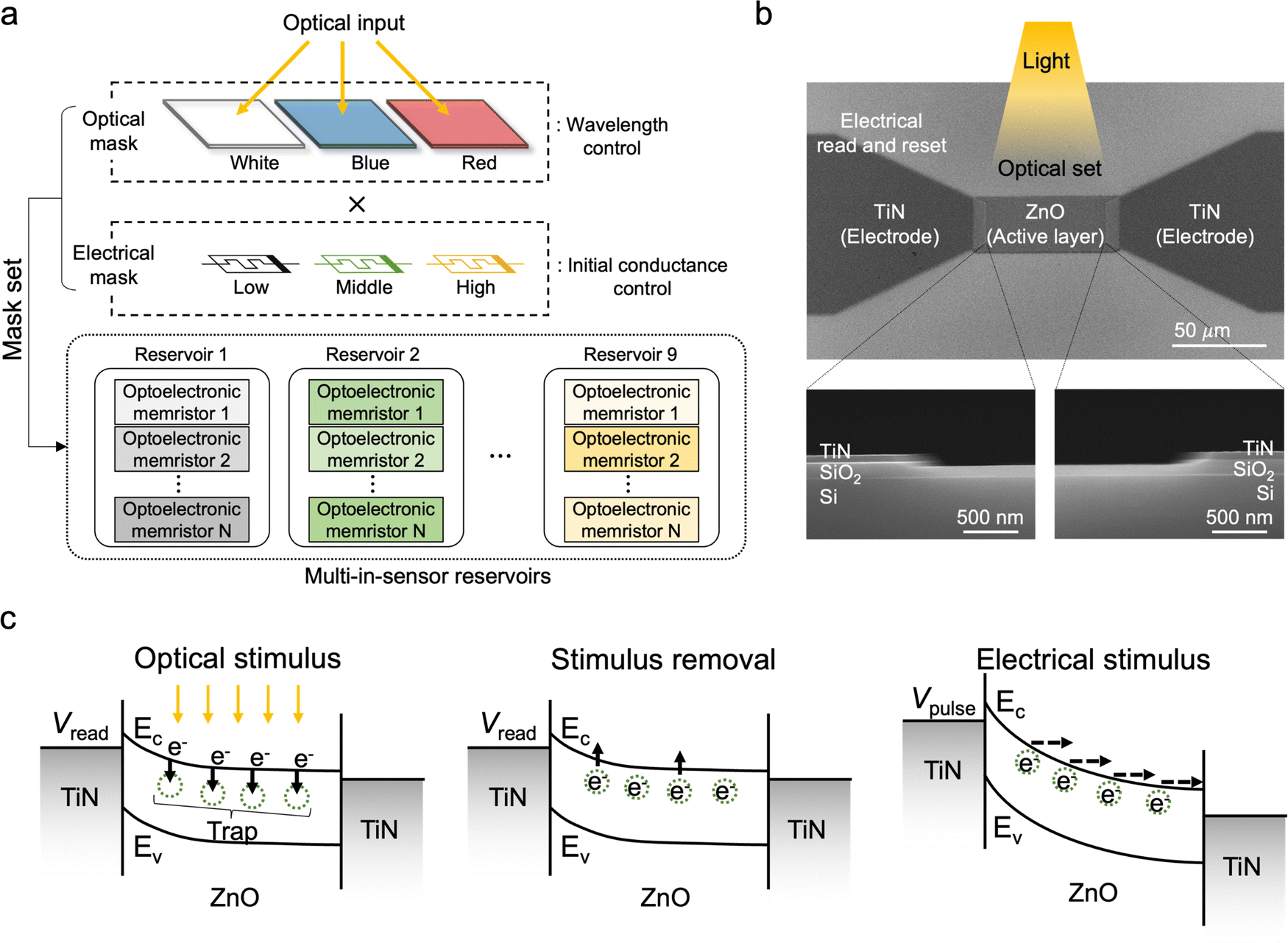 | ||
| Fig. 1 High-dimensional in-sensor reservoir computing (RC) using the ZnO optoelectronic memristor, (a) schematic illustrations of the proposed high-dimensional in-sensor RC system. The optical and electrical masks are utilized to make diverse distinguishable reservoir states and enhance the dimensionality of RC. (b) Planar view (upper panel) and cross-sectional (lower panel) scanning electron microscopy images of the ZnO optoelectronic memristor with a line cell structure. (c) Schematic illustrations showing the operating principle of the ZnO optoelectronic memristor. Optical and electrical stimuli can change the conductance of the device. | ||
Results and discussion
ZnO optoelectronic memristors
In this work, ZnO was used as an active layer of the optoelectronic memristor due to its excellent photoactivity.26,34 As shown in the planar view (upper panel) and cross-sectional (lower panel) scanning electron microscopy (SEM) images of Fig. 1b, a line cell structure was designed to maximize the light-receiving area, where the TiN electrodes were positioned on the sides of the ZnO active layer. The detailed fabrication process is explained in Fig. S1 (ESI†) and the Experimental section. Fig. 1c illustrates the operating principle of the ZnO optoelectronic memristor. When an optical stimulus is applied, the electrons become excited and are captured by trap sites associated with oxygen vacancies.29 As these trap sites are filled, the Fermi level approaches the conduction band, increasing the number of free electrons. Consequently, the conductance of the device is increased by an optical stimulus. Upon removal of the optical stimulus, the trapped electrons gradually escape due to thermal disturbance, which refers to the random motion of electrons caused by their thermal energy. Such thermal disturbance decreases conductance and short-term plasticity (STP) behavior.29,35 This characteristic is typical of optoelectronic memristors in in-sensor RC systems.25–30 It should be noted that optical behavior depends on the wavelength of light, as photonic energy is determined by the wavelength. This wavelength dependency can be utilized to implement the optical mask, enabling the achievement of high dimensionality in in-sensor RC systems. In addition to an optical stimulus, the device's conductance can be altered by applying an electrical stimulus. When a negative voltage is applied, the trapped electrons quickly escape due to the electric field, resulting in a decrease in the conductance. The initial conductance of the device before applying an optical stimulus can be controlled to implement an electrical mask, further enhancing the dimensionality of in-sensor RC systems.The optoelectronic properties of the fabricated ZnO optoelectronic memristor were verified by measuring its current–voltage (I–V) characteristics, as shown in the left panel of Fig. 2a. A white light stimulus with an intensity of 5 mW cm−2 was applied during the positive sweeps. As a result of the light illumination, the device transitioned into a low-resistance state (LRS), confirming the optical SET process. During the negative sweeps, the device gradually returned to a high-resistance state (HRS) due to negative voltage application, confirming the electrical RESET process.
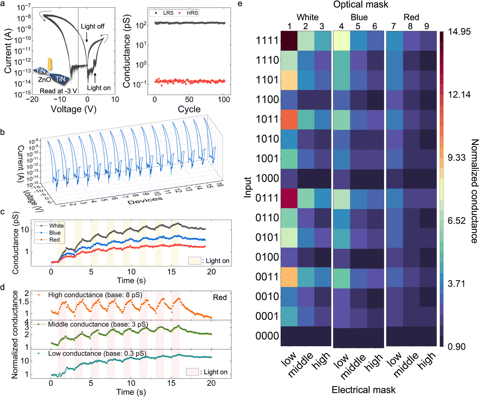 | ||
| Fig. 2 The optoelectronic properties of the fabricated ZnO optoelectronic memristor. (a) Current–voltage (I–V) characteristics and extracted conductance from 100 cycles. Optical SET was utilized to change the device to a low-resistance state (LRS), and electrical RESET was employed to change the device to a high-resistance state (HRS). (b) I–V characteristics of 16 independent devices indicating minimal device-to-device variation. The conductance change under optical pulses at (c) various wavelengths (optical mask) and (d) various initial conductance (electrical mask). (e) A heatmap displaying the normalized conductance value after applying the various optical inputs depending on 9 different mask sets, which are the combinations of 3 optical masks and 3 electrical masks. Each mask set is identified using numbers 1 to 9. | ||
The conductance values obtained from 100 consecutive optical SET and electrical RESET cycles are presented in the right panel of Fig. 2a, demonstrating excellent cycle-to-cycle uniformity. The conductance values were extracted at a reading voltage. In this study, a consistent −3 V read voltage was used, and Fig. S2 (ESI†) demonstrates that the read operation at −3 V does not affect the memristor's conductance. The results of Fig. 2a show that the fabricated device exhibits an exceptional on/off ratio exceeding 103 at the read voltage, outperforming prior research on optoelectronic memristors.12,29,36 This substantial switching range not only offers sufficient capacity for representing various input patterns but also facilitates the implementation of the masking process, thereby contributing to the establishment of a high-dimensional reservoir state. The operation of the ZnO optoelectronic memristor is not associated with capacitive effects or ferroelectric polarization and does not exhibit non-zero crossing I–V characteristics,37 as illustrated in Fig. S3 (ESI†). Additionally, Fig. 2b exhibits the I–V curves of 15 independent devices, indicating minimal device-to-device variation.
Fig. 2c and d depict the conductance changes observed while applying optical pulses. The conductance values were read at a voltage of −3 V. The optical pulses increased the conductance, attributed to the capture of electrons in trap sites, a common property of optoelectronic memristors. When the illumination was removed, the conductance gradually decayed as the trapped electrons were released. This phenomenon represents a typical light-induced STP mechanism employed to achieve in-sensor RC.23,25–29 Besides, pair-pulse facilitation (PPF) results from STP, which plays a vital role in biological synapse function.29 To further substantiate the presence of STP in this device, an additional experiment was conducted to measure the PPF characteristics. When a pair of optical pulses are applied, the PPF ratio is defined as A2/A1, where A1 represents the conductance resulting from the first pulse, and A2 represents the conductance resulting from the second pulse. In devices exhibiting STP, the PPF ratio is influenced by the pulse interval (Δt) due to a decrement in conductance over time. As shown in Fig. S4 (ESI†), the PPF ratio decreased from 1.3 to 1.08 when Δt increased from 0.1 s to 1.0 s, confirming the STP in this device.
Two parameters were controlled to manipulate the conductance changes. First, the wavelengths of the light were varied, and second, the initial conductance of the device was modulated. Wavelength modulation was achieved using an optical mask, while the initial conductance modulation was accomplished using an electrical mask. These masks enabled high-dimensional operations within the in-sensor RC.
The optical masks, controlling the wavelengths, were achieved using colored cellophane papers for filtering while generating identical optical pulses from the light source. Three different kinds of cellophane papers were used for masking: transparent cellophane paper for white light illumination, blue-colored cellophane paper for blue light illumination, and red-colored cellophane paper for red light illumination. It is worth noting that these colored cellophane papers can be substituted with a color filter array, commonly used in practical applications of image sensors.38,39 As shown in Fig. 2c, when the cellophane papers had colors, the increase in conductance due to optical pulses became smaller, as only photons with specific wavelengths were applied to the device. When the red-colored cellophane paper was used as the mask, the conductance increase was smaller than the blue-colored cellophane paper, owing to the lower photonic energy of red light.40 The decay rate was slower when illuminated with red light, as the activation energy at the lower conductance state is higher, and electrons rarely escape from the trap sites. For the quantitative activation energy analysis, the time-dependent current-relaxation characteristics were measured, as shown in Fig. S5 (ESI†). From the Arrhenius plots, the activation energies of the low and high conductance states were extracted as 0.27 eV and 0.18 eV, respectively.41 Because of the higher activation energy, it was difficult to detrap the trapped electrons from the trap sites at the lower conductance state formed by red light illumination.
On the other hand, with the electrical masks, the initial conductance of the device was regulated by applying negative electrical pulses before exposing it to light. The trapped electrons were released by applying negative voltages. Modifying the initial conductance can result in various reservoir states, as the optical response varies based on the initial conductance. Fig. S6 (ESI†) shows the conductance as a function of the number of electrical pulses. Such conductance modulation was utilized to control the initial conductance for the operation of the electrical mask. For example, memristors with three distinct initial conductance states can be created by not applying any electrical pulses to the first memristor (low initial conductance), applying a small number of negative electrical pulses to the second memristor (middle initial conductance), and applying a large number of negative electrical pulses to the third memristor (high initial conductance). As the initial conductance increased, the conductance increase by optical pulses became smaller because a significant number of electrons were already trapped at the trap sites, as shown in Fig. 2d. The decay rate was faster when the initial conductance was high, primarily because the activation energy was lower, allowing electrons to escape the trap sites more easily. Note that this behavior differs from that of the optical mask used for wavelength modulation. In the case of the optical mask, the increase and decay were lower at longer wavelengths (red light). However, in the case of the electrical mask, the increase rate was lower at higher initial conductance, while the decay was activated. These distinct characteristics of the optical and electrical masks can help represent various distinguishable reservoir states, thereby enhancing the dimensionality of the in-sensor RC system with minimal correlation.
Fig. 2e depicts the heatmaps showing the normalized conductance value after applying different optical inputs, representing the operations of the optical reservoir. The input stream consisted of four optical pulses, corresponding to the input bits ranging from ‘0000’ to ‘1111’ for the 4-bit in-sensor reservoir operations.42 The current at each bit was measured at 0.1 s after the optical pulses, while a reading voltage was set to −3 V. The detailed measurement setup for the in-sensor reservoir operations is explained in Fig. S7 (ESI†) and the experimental section. The initial conductance used for each optical mask is summarized in Table S1 (ESI†). Notably, all 16 reservoir states were distinguishable, demonstrating the successful experimental implementation of in-sensor RC. It is essential to highlight that even when the same input stream was applied, the conductance varied depending on the wavelength (optical mask) and initial conductance (electrical mask). This finding implies that different optical and electrical masks can represent a wide range of distinguishable reservoir states, enhancing the dimensionality of the in-sensor RC system. In this work, 9 mask sets were employed, comprising combinations of 3 optical masks and 3 electrical masks. As depicted in Fig. 2e, each mask set was assigned a numerical name ranging from 1 to 9. Considering that the current passing through the ZnO optoelectronic memristor ranges from 1 to 400 pA, and the reading voltage is set at 3 V, the power consumption is within the range of 0.003 to 1.2 nW. This value is lower than from previous studies, which is attributed to the low operation current of the ZnO optoelectronic memristor.25–30
As previously mentioned, the distinct characteristics of the optical and electrical masks play a crucial role in representing various distinguishable reservoir states. Fig. 3 shows the conductance of the ZnO memristor at each time step (t1–t4) when applying 4-bit inputs, demonstrating the significance of adopting two different types of masks (optical and electrical). The results in Fig. 3 include the 5 repeated measurements on a total of 16 devices for each input pattern and the 4 mask sets, revealing the reproducibility of the results. As shown in Fig. 3a, the input patterns ‘1001’, ‘1110’, and ‘0101’ were not distinguishable when mask set 1 (white light and low initial conductance state) was used. However, Fig. 3b shows that the ‘0101’ pattern became distinguishable when mask set 3 (white light and high initial conductance state) was applied, showing the impact of the electrical mask. Specifically, the conductance difference between ‘1110’ and ‘0101’ significantly increased from 3% to 20% when changing mask set 1 to mask set 3. In this mask set, the ZnO optoelectronic memristor experienced weaker potentiation and stronger relaxation than in mask set 1.
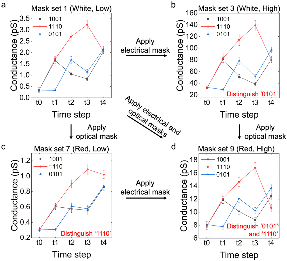 | ||
| Fig. 3 The distinguishable output of 4-bit reservoir states by adopting optical and electrical masks. The average and standard deviations for the 80 measurements (5 repeat in 16 devices) were plotted using symbols and error bars, respectively. (a) Conductance of the ZnO memristor at each time step when the input patterns ‘1001’, ‘1110’, and ‘0101’ were applied. The initial mask set (white and low) does not exhibit the three input patterns. (b) Distinction of the ‘0101’ pattern by applying the electrical mask. (c) Distinction of the ‘1110’ pattern by applying the optical mask. (d) Distinction of all three patterns by combining both optical and electrical masks. | ||
On the other hand, when employing mask set 7 (red light and low initial conductance state), the ‘1110’ pattern became distinguishable, as shown in Fig. 3c, highlighting the effect of the optical mask. In this mask set, the device underwent stronger potentiation due to the longer wavelength, leading to a weaker relaxation effect. As a result of the reduced relaxation, mask set 7 enhanced the capacity to detect ‘1’ in the input pattern, leading to a significant increase in the conductance of the ‘1110’ pattern. As shown in Fig. 3d, all three patterns became distinguishable by applying mask set 9 (red light and high initial conductance state), showing that combining both masks is essential. Mask set 9 minimized the potentiation effect while providing substantial relaxation, enabling clear differentiation among the three patterns. It should be noted that the effectiveness of the mask set in distinguishing patterns varies depending on the patterns themselves. Therefore, it is essential to create diverse reservoir states by utilizing different mask sets. Such various distinguishable reservoir states enhance the dimensionality and significantly improve the performance of the in-sensor RC system, which will be further discussed in the following sections.
Motion perception using the ZnO optoelectronic memristor array
Fig. 4 shows the motion perception using a 4 × 4 array of 16 ZnO optoelectronic memristors. As illustrated in Fig. 4a, it was attempted to distinguish the clockwise and counter-clockwise motions of a cross-pattern. As time passed from t1 to t4, an optical pulse was applied to each ZnO optoelectronic memristor corresponding to each pixel when the pattern was detected (white pixel), and no pulse was applied when the pattern was not detected (black pixel). For instance, for the clockwise motion, an input stream of ‘0001’ was applied to the pixel located in the first column of the third row, while ‘0100’ was applied for the counter-clockwise motion. Fig. 4b shows the heatmaps representing the normalized conductance value of each ZnO optoelectronic memristor for both motions when 9 different mask sets (1 to 9) were applied. It is worth noting that the heatmaps of the two motions exhibit similar distributions with the same mask set, making it difficult to classify the two motions using a single mask set. However, the combination of various optical and electrical masks allows for generating multiple reservoir states, thereby enhancing the dimensionality of the in-sensor RC system. Fig. 4c shows the Pearson correlation matrix, which is determined by the following equation: | (1) |
 and
and 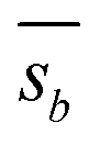 are the averages of each vector element.43 The reservoir states generated by different mask sets were not correlated with each other due to the distinct properties of the optical and electrical masks. To evaluate the quantitative impact of this high-dimensional in-sensor RC system on classification accuracy, a software simulation was conducted. Training and test datasets were created by intentionally introducing variations to the measured data. These datasets were then fed into a readout network consisting of a single layer to classify clockwise and counter-clockwise motions, as illustrated in Fig. 4d. As a result, two motions were classified with 100% accuracy when all 9 mask sets were employed, thanks to the high dimensionality (Fig. 4e). In contrast, low accuracy was obtained when only a single mask set was used. The confusion matrix depicted in Fig. 4f demonstrates that successful classification was achieved when all 9 mask sets were utilized. Motion perception was accomplished by employing a simulated readout network that utilized the measurement data from the ZnO optoelectronic memristor as input. A detailed explanation of the step-by-step process of motion perception can be found in Fig. S8 (ESI†).
 | ||
| Fig. 4 Motion perception using the fabricated ZnO optoelectronic memristor array, (a) schematic illustrations depicting two different motions of a cross-pattern: clockwise and counter-clockwise. (b) The heatmaps displaying the normalized conductance values obtained for both motions when 9 mask sets (1 to 9) were adopted. (c) The Pearson correlation matrix presenting the correlation coefficient between the two mask sets. (d) Schematic illustrations representing the in-sensor RC system, which comprises an optical mask, an electrical mask, and a readout network. (e) The classification accuracies as a function of the number of training epochs. Higher accuracy was achieved when all 9 mask sets were used compared to when only a single mask set was employed. (f) Confusion matrix when a single mask set was used, and all 9 mask sets were employed. | ||
MNIST pattern classification using high-dimensional in-sensor RC
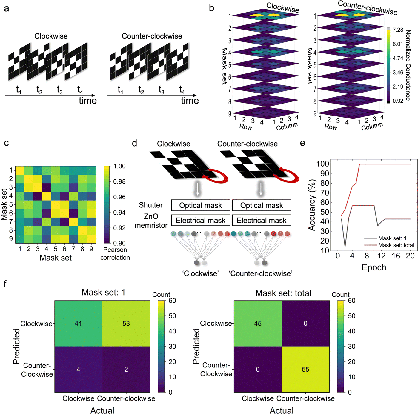
To evaluate the network's performance and compare it to previous studies, handwritten digit classification was performed using the MNIST dataset, which had 60![[thin space (1/6-em)]](https://www.rsc.org/images/entities/char_2009.gif) 000 digits for training and 10000 digits for testing. The pixel values were binarized, and the 28 × 28 images were chopped into 4-bit segments to apply a 4-bit optical pulse stream to the ZnO optoelectronic memristor, as illustrated in Fig. 5a.44 The measured conductance from each mask set (Fig. 2e) comprised the reservoir state representing each image. Consequently, a 196 × 1 conductance vector is generated for each mask set, and the combination of the conductance vectors of the mask sets is input to the readout network. Depending on the number of mask sets utilized (N), the readout network comprised 196 × N input and 10 output neurons.
000 digits for training and 10000 digits for testing. The pixel values were binarized, and the 28 × 28 images were chopped into 4-bit segments to apply a 4-bit optical pulse stream to the ZnO optoelectronic memristor, as illustrated in Fig. 5a.44 The measured conductance from each mask set (Fig. 2e) comprised the reservoir state representing each image. Consequently, a 196 × 1 conductance vector is generated for each mask set, and the combination of the conductance vectors of the mask sets is input to the readout network. Depending on the number of mask sets utilized (N), the readout network comprised 196 × N input and 10 output neurons.
 | ||
| Fig. 5 MNIST pattern classification using high-dimensional in-sensor RC. (a) Schematic illustrations of the in-sensor RC system for MNIST pattern classification. (b) The classification accuracy depends on the mask set when a single mask set was used with low dimensionality. (c) The classification accuracy as a function of the correlation coefficient when two mask sets were used. (d) The Pearson correlation matrix shows the correlation coefficient of the two mask sets and the confusion matrix shows the classification accuracy of each case. (e) The classification accuracy of four cases when only mask set 1 was used, when mask sets 1 and 3 were used, when mask sets 1 and 7 were used, and when mask sets 1, 3 and 7 were used. (f) The classification accuracy as a function of the number of training epochs, contrasting the adoption of a single mask set with the adoption of all 9 mask sets. (g) Confusion matrix for each case. | ||
As shown in Fig. 5b, the classification accuracy was low when a single mask set was utilized due to the limited dimensionality. However, when two mask sets were employed, the classification accuracy improved to over 91%. It should be noted that the classification accuracy was inversely proportional to the correlation coefficient between the two mask sets, as demonstrated in Fig. 5c. For a detailed analysis, the Pearson correlation matrix shows the correlation coefficient between the reservoir states generated by two mask sets and the confusion matrix displays the classification accuracy, which are shown in Fig. 5d. These results suggest that diverse dynamics in reservoir operations are necessary to achieve high performance, which is why this study adopted two different types of masks (optical and electrical). Fig. 5e exhibits the classification accuracies of four cases: when only mask set 1 was used as the baseline, when mask sets 1 and 3 were used to observe the effect of the electrical mask, when mask sets 1 and 7 were used to observe the effect of the optical mask, and when mask sets 1, 3 and 7 were used to examine the combined effects of the electrical and optical masks. The classification accuracy could be further enhanced when both electrical and optical masks were employed, thanks to the increased dimensionality. Notably, the accuracy was higher when combining the electrical and optical masks rather than using three electrical or optical masks separately (Fig. S9, ESI†). This is because electrical and optical masks can represent various distinguishable reservoir states, thus enhancing the dimensionality of the in-sensor RC system with minimal correlation. Fig. 5f shows the classification accuracy as a function of the number of training epochs, comparing the use of a single mask set with the utilization of all 9 mask sets, which are the combinations of 3 optical and 3 electrical masks. Furthermore, Fig. 5g presents the confusion matrix for each case. The successful classification was achieved with an accuracy of 94.1% when all 9 mask sets were employed, which is the highest accuracy among previously reported in-sensor RC works.27,29 Notably, this outstanding performance in MNIST recognition was accomplished using a readout network that consisted of a single layer without any hidden layers. To further validate these outcomes, the impact of device variations was tested. Cycle-to-cycle (C2C) and device-to-device (D2D) variations were included in the recognition process. Based on normal distributions with an average (μ) of 1 and various standard deviations (σ), random scale factors with errors were incorporated into the training and inference of MNIST images. C2C variation was introduced to induce variations in device responsiveness across different samples, whereas D2D variation was employed to generate variations in device responsiveness within a specific sample. Fig. S10 (ESI†) shows the RC performance based on the various σ/μ ratios of 0–0.125, including the experimental C2C and D2D variation values obtained from the DC cycling test (Fig. 2a) and the device variation test (Fig. 2b). This result demonstrated the robustness of classification accuracy even with C2C or D2D variations.
Employing multiple mask sets in parallel proves efficient for creating a high-dimensional reservoir state. This approach significantly enhances system performance but increases the number of optoelectronic memristors. Therefore, the power consumption of reservoirs will increase when there are too many optoelectronic memristors, while the speed remains constant due to their parallel operation. However, it should be noted that the power consumption of the entire system can be reduced by simplifying the readout network. Remarkably, in this work, high accuracies were achieved even with a single-layer readout network, which can significantly decrease the power consumption of the entire system by reducing training synapses and training costs. Besides, a ‘mask blending’ technique can be adopted to enhance the performance without increasing the number of optoelectronic memristors. Blending multiple masks to specific regions can yield better results since frequently appearing patterns differ from region to region. When red, blue, and white masks were applied to the central, border, and edge sections of the 20 × 20 image, an improved accuracy of 90.35% was achieved while reducing the number of optoelectronic memristors by approximately 50% compared to the case using a single mask set based on 196 memristors (Fig. S11, ESI†). Therefore, achieving high accuracy while reducing the number of optoelectronic memristors is possible, reducing power consumption.
Human action pattern recognition using high-dimensional in-sensor RC
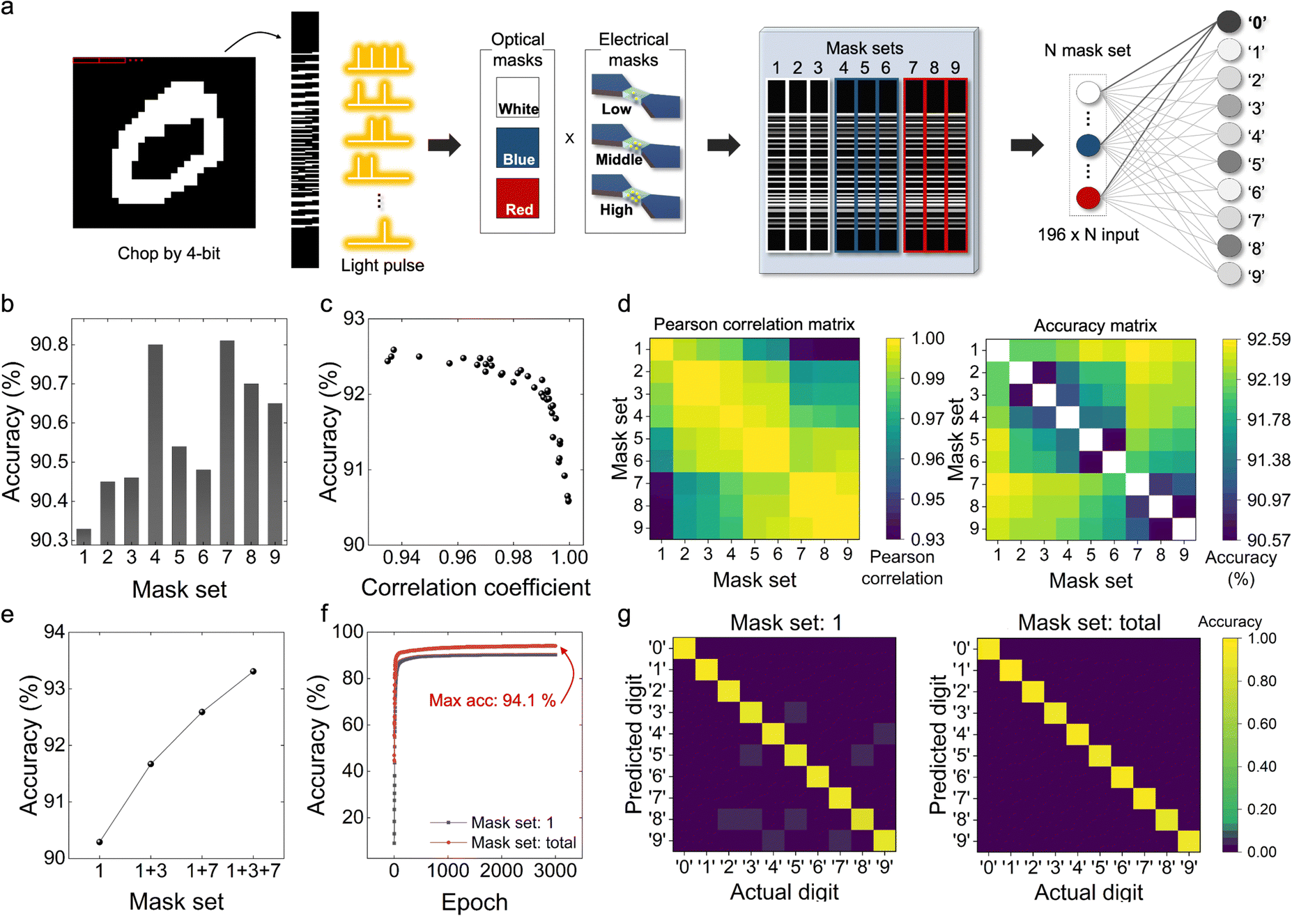
Finally, human action pattern recognition was demonstrated to show its capability for complex motion perception. The human action patterns, comprising 10 activities including bending, jacking, jumping, p-jumping (jumping in position), running, siding, skipping, walking, wave1 (in one hand) and wave2 (in two hands), were taken from the Weizmann dataset.45 A total of 90 sample videos were collected for the dataset, with each action being performed by a group of 9 individuals. The simulation was carried out using 4-frame units composed of 70 × 30 pixels by deleting unused borders from the original datasets (Fig. S12, ESI†), which is an identical preprocessing method used in the previous study.28 Considering practical visual scenarios, 4-frame units were constructed at 5-frame intervals in each sample video rather than utilizing long-range averaging. A total of 3345 4-frame units were generated from the sample video, resulting in a dataset size of 3345 × 2100 for one mask set. 80% of the dataset was used for training, while the remaining 20% was used for testing to guarantee the evaluation of a precise model. As time passed from t1 to t4, an optical pulse was applied to each ZnO optoelectronic memristor corresponding to each pixel when the human was detected (white pixel), and it was not applied when the human was not detected (black pixel), as illustrated in Fig. 6a. The measured conductance of each reservoir state shown in Fig. 2d was then fed into a single-layer readout network. When employing N mask sets, the readout network consisted of 2100 × N input and 10 output neurons. | ||
| Fig. 6 Human action pattern recognition using high-dimensional in-sensor RC. (a) Schematic illustrations of the in-sensor RC system for human action pattern recognition. (b) The classification accuracy as a function of the number of mask sets. (c) The classification accuracy as a function of the number of training epochs when a single mask set was used, and all 9 mask sets were employed. (d) Confusion matrix for each case. | ||
As shown in Fig. 6b, it is evident that the recognition accuracy increased as the number of mask sets increased, thanks to the higher dimensionality. Fig. 6c depicts the recognition accuracy as a function of the number of training epochs, comparing the use of only one mask set versus all 9 mask sets, which are the combinations of 3 optical and 3 electrical masks. Furthermore, Fig. 6d shows the confusion matrix for each case. The recognition accuracies for all mask set combinations are presented in Fig. S13 (ESI†). When all 9 mask sets were used, successful recognition was achieved with a remarkable accuracy of 99.4% while using a single-layer readout network with 189000 training synapses. It should be emphasized that this result is higher than that observed in previous literature (97.14%),28 even though previous literature employed a multi-layer readout network with 211000 training synapses. In this in-sensor RC system, the mask set combination can be flexibly adjusted, allowing for the selective utilization of mask sets to achieve additional savings in training synapses and training costs. For example, when employing three mask sets, an accuracy rate of 98.44% was achieved while reducing the number of training parameters to 63000. This significant improvement was attributed to the high dimensionality of our in-sensor RC system, which incorporates optical and electrical masks. The impact of device variation on system performance was tested to validate the results further. C2C and D2D variations were incorporated into the human action recognition process, similar to the variation test in MNIST recognition. The results of the variation test shown in Fig. S14 (ESI†) demonstrated the robustness of classification accuracy in the presence of C2C or D2D variations.
Conclusions
A high-dimensional in-sensor RC system with ZnO optoelectronic memristors was demonstrated for high-performance neuromorphic machine vision. The system achieved remarkable accuracy in pattern classification and motion perception by employing optical and electrical masks capable of generating diverse distinguishable reservoir states. Among the previously reported in-sensor RC works, the highest classification accuracy of 94.1% was accomplished using the MNIST dataset (Table S2, ESI†). Importantly, it was discovered that incorporating both optical and electrical masks, rather than relying on a single type of mask, significantly improved the classification accuracy. Human action pattern recognition was successfully performed with a high accuracy of 99.4%, showing its excellent capability for complex motion perception. Notably, these successes were attained by using a single-layer readout network, which can drastically reduce the network size and training costs. The proposed high-dimensional in-sensor RC system will open a new avenue for superior performance in neuromorphic machine vision applications, including object detection, motion perceptions, and robotics.Experimental section/methods
Device fabrication
As a starting substrate, a thermally oxidized silicon wafer was used. First, the 50 nm-thick TiN layer was deposited by sputtering (Endura, Applied Materials) and patterned by photo-lithography and dry etching. Next, the ZnO active layer was formed by atomic layer deposition (ALD) utilizing a traveling-wave-type ALD reactor (CN-1 Co. Plus 200). Diethylzinc [DEZn, (C2H5)2Zn] and ozone generated by a plasma discharge of O2 gas were used as Zn-precursor and oxygen sources, respectively. The ZnO layer was patterned by photo-lithography and dry etching. A line cell structure was designed to maximize the light-receiving area, where the TiN electrodes were positioned on the sides of the ZnO active layer. Fig. S1 (ESI†) shows the details of the fabrication process.Electrical measurement
Measurements of the electrical characteristics were conducted using a semiconductor parameter analyzer (4155A, Hewlett Packard).Optical test
White light illumination was applied with a lamp power supply (MHF-D100LR, Moritex). An extra fast optical shutter (X-FOS, LC-Tec) controlled the application of optical pulses to the device by receiving the pulse stream from the pulse generator (B1110A, Agilent). Transparent cellophane paper, blue-colored cellophane paper, and red-colored cellophane paper were used to control the wavelength.SEM analysis
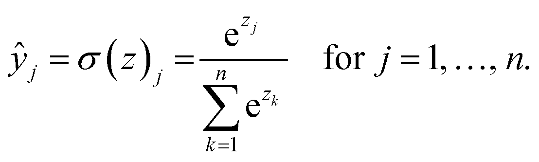
SEM images were taken using a field emission SEM (S-4800, Hitachi).900 for human action pattern recognition), was multiplied by the weight matrix (W) of the readout layer. This multiplication resulted in the weighted sum (z).| z = WT·x | (2) |
 | (3) |
 | (4) |
Author contributions
Y. H. Jang and J.-K. Han contributed equally to this work. Y. H. Jang and J.-K. Han conceived the research idea. Y. H. Jang and S. Moon fabricated the device. Y. H. Jang and J.-K. Han performed the measurement. Y. H. Jang, S. K. Shim, J. Han, S. Cheong, and S. H. Lee performed the software simulation. Y. H. Jang and J.-K. Han wrote the manuscript. C. S. Hwang supervised the whole research and edited the manuscript.Conflicts of interest
There are no conflicts to declare.Acknowledgements
This work was supported by the National Research Foundation of Korea (Grant no. 2020R1A3B2079882).Notes and references
- F. Liao, F. Zhou and Y. Chai, J. Semicond., 2021, 42(1), 013105 CrossRef.
- A. Fayyazi, M. Ansari, M. Kamal, A. Afzali-Kusha and M. Pedram, IEEE Internet Things J., 2018, 5(2), 1011–1022, DOI:10.1109/JIOT.2018.2799948.
- F. Zhou and Y. Chai, Nat. Electron., 2020, 3(11), 664–671, DOI:10.1038/s41928-020-00501-9.
- J. Zhu, T. Zhang, Y. Yang and R. Huang, Appl. Phys. Rev, 2020, 7(1), 011312, DOI:10.1063/1.5118217.
- J. K. Han, S. Y. Yun, S. W. Lee, J. M. Yu and Y. K. Choi, Adv. Funct. Mater., 2022, 32, 1–17 Search PubMed.
- L. Mennel, J. Symonowicz, S. Wachter, D. K. Polyushkin, A. J. Molina-Mendoza and T. Mueller, Nature, 2020, 579(7797), 62–66, DOI:10.1038/s41586-020-2038-x.
- Y. Chai, Nature, 2020, 32–33 CrossRef CAS PubMed.
- J. K. Han, Y. W. Chung, J. Sim, J. M. Yu, G. B. Lee, S. H. Kim and Y. K. Choi, Sci. Rep., 2022, 12(1), 1818, DOI:10.1038/s41598-022-05944-y.
- Y. Wang, Y. Gong, L. Yang, Z. Xiong, Z. Lv, X. Xing, Y. Zhou, B. Zhang, C. Su, Q. Liao and S. T. Han, Adv. Funct. Mater., 2021, 31(21), 2100144, DOI:10.1002/adfm.202100144.
- F. Zhou, Z. Zhou, J. Chen, T. H. Choy, J. Wang, N. Zhang, Z. Lin, S. Yu, J. Kang, H. S. P. Wong and Y. Chai, Nat. Nanotechnol., 2019, 14(8), 776–782, DOI:10.1038/s41565-019-0501-3.
- A. Emboras, A. Alabastri, P. Lehmann, K. Portner, C. Weilenmann, P. Ma, B. Cheng, M. Lewerenz, E. Passerini, U. Koch, J. Aeschlimann, F. Ducry, J. Leuthold and M. Luisier, Appl. Phys. Lett., 2020, 117(23), 230502, DOI:10.1063/5.0028539.
- L. Hu, J. Yang, J. Wang, P. Cheng, L. O. Chua and F. Zhuge, Adv. Funct. Mater., 2021, 31(4), 2005582, DOI:10.1002/adfm.202005582.
- S. W. Cho, C. Jo, Y. H. Kim and S. K. Park, Nano-Micro Lett., 2022, 14(1), 203, DOI:10.1007/s40820-022-00945-y.
- G. Cao, P. Meng, J. Chen, H. Liu, R. Bian, C. Zhu, F. Liu and Z. Liu, Adv. Funct. Mater., 2021, 31(4), 2005443, DOI:10.1002/adfm.202005443.
- Y. Cai, F. Wang, X. Wang, S. Li, Y. Wang, J. Yang, T. Yan, X. Zhan, F. Wang, R. Cheng, J. He and Z. Wang, Adv. Funct. Mater., 2023, 33(5), 2212917, DOI:10.1002/adfm.202212917.
- Y. Pei, L. Yan, Z. Wu, J. Lu, J. Zhao, J. Chen, Q. Liu and X. Yan, ACS Nano, 2021, 15(11), 17319–17326, DOI:10.1021/acsnano.1c04676.
- X. Yan, Y. Pei, H. Chen, J. Zhao, Z. Zhou, H. Wang, L. Zhang, J. Wang, X. Li, C. Qin, G. Wang, Z. Xiao, Q. Zhao, K. Wang, H. Li, D. Ren, Q. Liu, H. Zhou, J. Chen and P. Zhou, Adv. Mater., 2019, 31(7), 1805284, DOI:10.1002/adma.201805284.
- C. Yang, B. Sun, G. Zhou, T. Guo, C. Ke, Y. Chen, J. Shao, Y. Zhao and H. Wang, ACS Mater. Lett., 2023, 5(2), 504–526, DOI:10.1021/acsmaterialslett.2c00911.
- C. Du, F. Cai, M. A. Zidan, W. Ma, S. H. Lee and W. D. Lu, Nat. Commun., 2017, 8, 1–10 CrossRef CAS.
- J. Moon, W. Ma, J. H. Shin, F. Cai, C. Du, S. H. Lee and W. D. Lu, Nat. Electron., 2019, 2, 480–487 CrossRef.
- R. Midya, Z. Wang, S. Asapu, X. Zhang, M. Rao, W. Song, Y. Zhuo, N. Upadhyay, Q. Xia and J. J. Yang, Adv. Intell. Syst., 2019, 1, 1900084 CrossRef.
- Y. Zhong, J. Tang, X. Li, B. Gao, H. Qian and H. Wu, Nat. Commun., 2021, 12(1), 408, DOI:10.1038/s41467-020-20692-1.
- Y. Zhong, J. Tang, X. Li, X. Liang, Z. Liu, Y. Li, Y. Xi, P. Yao, Z. Hao, B. Gao, H. Qian and H. Wu, Nat. Electron., 2022, 5, 672–681 CrossRef.
- Y. H. Jang, S. H. Lee, J. Han, W. Kim, S. K. Shim, S. Cheong, K. S. Woo, J. K. Han and C. S. Hwang, Adv. Mat., 2023, 2309314, DOI:10.1002/adma.202309314.
- L. Sun, Z. Wang, J. Jiang, Y. Kim, B. Joo, S. Zheng, S. Lee, W. J. Yu, B. S. Kong and H. Yang, Sci. Adv., 2021, 7(20), eabg1455, DOI:10.1126/sciadv.abg1455.
- W. Du, C. Li, Y. Huang, J. Zou, L. Luo, C. Teng, H. C. Kuo, J. Wu and Z. Wang, IEEE Electron Device Lett., 2022, 43(3), 406–409, DOI:10.1109/LED.2022.3142257.
- K. Liu, T. Zhang, B. Dang, L. Bao, L. Xu, C. Cheng, Z. Yang, R. Huang and Y. Yang, Nat. Electron., 2022, 5, 761–773 CrossRef CAS.
- Z. Zhang, X. Zhao, X. Zhang, X. Hou, X. Ma, S. Tang, Y. Zhang, G. Xu, Q. Liu and S. Long, Nat. Commun., 2022, 13, 1–9 Search PubMed.
- Y. Sun, Q. Li, X. Zhu, C. Liao, Y. Wang, Z. Li, S. Liu, H. Xu and W. Wang, Adv. Intell. Syst., 2023, 5(1), 2200196, DOI:10.1002/aisy.202200196.
- J. Chen, Z. Zhou, B. J. Kim, Y. Zhou, Z. Wang, T. Wan, J. Yan, J. Kang, J. H. Ahn and Y. Chai, Nat. Nanotechnol., 2023, 1–7, DOI:10.1038/s41565-023-01379-2.
- M. Lukoševičius and H. Jaeger, Comput. Sci. Rev., 2009, 3, 127–149 CrossRef.
- L. Appeltant, M. C. Soriano, G. Van Der Sande, J. Danckaert, S. Massar, J. Dambre, B. Schrauwen, C. R. Mirasso and I. Fischer, Nat. Commun., 2011, 2(1), 468, DOI:10.1038/ncomms1476.
- G. Tanaka, T. Yamane, J. B. Héroux, R. Nakane, N. Kanazawa, S. Takeda, H. Numata, D. Nakano and A. Hirose, Neural Networks, 2019, 115, 100–123 CrossRef PubMed.
- B. Dang, K. Liu, X. Wu, Z. Yang, L. Xu, Y. Yang and R. Huang, Adv. Mater., 2023, 35(37), 2204844, DOI:10.1002/adma.202204844.
- R. Khan, N. U. Rehman, N. Ilyas, N. Sfina, M. Barhoumi, A. Khan, K. Althubeiti, S. Al Otaibi, S. Iqbal, N. Rahman, M. Sohail, A. Ullah, T. Del Rosso, Q. Zaman, A. Ali Khan, S. S. Abdullaev and A. Khan, Nanoscale, 2023, 15(4), 1900–1913, 10.1039/d2nr05257a.
- T. Y. Wang, J. L. Meng, Q. X. Li, Z. Y. He, H. Zhu, L. Ji, Q. Q. Sun, L. Chen and D. W. Zhang, Nano Energy, 2021, 89, 106291, DOI:10.1016/j.nanoen.2021.106291.
- B. Sun, M. Xiao, G. Zhou, Z. Ren, Y. N. Zhou and Y. A. Wu, Mater. Today Adv., 2020, 6, 100056, DOI:10.1016/j.mtadv.2020.100056.
- R. Lukac and K. N. Plataniotis, IEEE Trans. Consum. Electron., 2005, 51(4), 1260–1267, DOI:10.1109/TCE.2005.1561853.
- E. Heydari, J. R. Sperling, S. L. Neale and A. W. Clark, Adv. Funct. Mater., 2017, 27(35), 1701866, DOI:10.1002/adfm.201701866.
- A. Darmont, White Pap., 2009, vol. 4, pp. 1–13.
- D. V. Lang, J. Appl. Phys., 1974, 45(7), 3023–3032, DOI:10.1063/1.1663719.
- Y. H. Jang, W. Kim, J. Kim, K. S. Woo, H. J. Lee, J. W. Jeon, S. K. Shim, J. Han and C. S. Hwang, Nat. Commun., 2021, 12(1), 5727, DOI:10.1038/s41467-021-25925-5.
- J. Benesty, J. Chen, Y. Huang and I. Cohen, Springer Topics in Signal Processing, 2009.
- A. Jalalvand, G. Van Wallendael and R. V. D. Walle, in Proceedings – 7th International Conference on Computational Intelligence, Communication Systems and Networks, CICSyN, 2015.
- M. Blank, L. Gorelick, E. Shechtman, M. Irani and R. Basri, Proceedings of the IEEE International Conference on Computer Vision, 2005.
- D. P. Kingma and J. L. Ba, 3rd International Conference on Learning Representations, ICLR 2015 – Conference Track Proceedings, 2015.
Footnotes |
| † Electronic supplementary information (ESI) available. See DOI: https://doi.org/10.1039/d3mh01584j |
| ‡ These authors contributed equally to this work. |
| This journal is © The Royal Society of Chemistry 2024 |