
Understanding radiation-generated electronic traps in radiation dosimeters based on organic field-effect transistors†
Derek
Dremann
a,
Evan J.
Kumar
 a,
Karl J.
Thorley
b,
Edgar
Gutiérrez-Fernández
cd,
James D.
Ververs
e,
J. Daniel
Bourland
ae,
John E.
Anthony
b,
Ajay Ram Srimath
Kandada
a and
Oana D.
Jurchescu
*a
a,
Karl J.
Thorley
b,
Edgar
Gutiérrez-Fernández
cd,
James D.
Ververs
e,
J. Daniel
Bourland
ae,
John E.
Anthony
b,
Ajay Ram Srimath
Kandada
a and
Oana D.
Jurchescu
*a
aDepartment of Physics and Center for Functional Materials (CFM), Wake Forest University, Winston Salem, NC 27109, USA. E-mail: jurchescu@wfu.edu
bUniversity of Kentucky Center for Applied Energy Research, Lexington, KY 40511, USA
cDepartment of Physics, University of Warwick, Gibbet Hill Road, Coventry, CV4 7AL, UK
dXMas/BM28-ESRF, 71 Avenue Des Martyrs, F-38043 Grenoble Cedex, France
eDepartment of Radiation Oncology, Wake Forest School of Medicine, Wake Forest University, Winston Salem, NC 27157, USA
First published on 27th October 2023
Abstract
Organic dosimeters offer unique advantages over traditional technologies, and they can be used to expand the capabilities of current radiation detection systems. In-depth knowledge of the mechanisms underlying the interaction between radiation and organic materials is essential for their widespread adoption. Here, we identified and quantitatively characterized the electronic traps generated during the operation of radiation dosimeters based on organic field-effect transistors. Spectral analysis of the trap density of states, along with optical and structural studies, revealed the origin of trap states as local structural disorder within the crystalline films. Our results provide new insights into the radiation-induced defects in organic dosimeters, and pave the way for the development of more efficient and reliable radiation detection devices.
New conceptsIncorporation of organic semiconductors into radiation dosimeters could make radiation detection more accessible and expand the applications to conformal, portable, and wearable technologies. Additionally, organic dosimeters can be tuned to be sensitive to specific types of radiation and could be more accurate in medical applications due to the similar response to radiation to the human body. Unlike most emerging technologies, however, the innovation witnessed in the field has outgrown our understanding of the phenomena responsible for this progress. In this study, we clarify the operation mechanism in radiation dosimeters based on organic field-effect transistors. Specifically, we demonstrate that the interaction between the radiation and organic semiconductors results in the formation of electronic traps and we quantitatively characterize these new states. We identify the local structural disorder as the main origin for the trap formation and we find a direct correlation between the radiation dose and the density of trap states. Our findings shed new light on the radiation-induced defects in organic semiconductors, and provide new strategies for increasing the sensitivity of organic dosimeters. |
Introduction
Radiation dosimetry is a critical technology with applications in a wide range of industries, including space exploration, energy generation, environmental safety, and medicine. Traditional radiation dosimeters are made from inorganic materials, such as silicon or germanium, but organic materials are increasingly being investigated for these applications due to their unique properties.1–3 These characteristics include low-cost processing, tunable sensitivity to specific radiation types granted by the chemical diversity, compatibility with a wide range of form factors, as well as biocompatibility.4–7 Organic-based flexible and conformal devices can be attached to curved surfaces or implanted in the body, making them extremely well-suited for wearable technologies and medical devices. Clinical applications where dosimeters are used include dental X-rays, fluoroscopic C-arms for operating rooms, mammography units, computerized tomography (CT) scans, nuclear medicine, or radiation oncology. The similarity in radiation response to that of the human body, owing to their similar atomic numbers (Z), ensures precise delivery of radiation to the site of treatment while minimizing the exposure of surrounding healthy tissue, which is essential for effective patient care. The prospect of achieving greater precision in radiation dosimetry while simultaneously reducing the cost of equipment has inspired the development of several new technologies for organic dosimeters.1,2,8–11 We recently demonstrated a proof-of-concept organic dosimeter based on organic field-effect transistor (OFET), which we named RAD-OFET, or radiation dosimeter based on OFET.2 This dosimeter can effectively detect doses between 0 Gy and 10 Gy with a sensitivity of up to 5.2 ± 0.3 × 10⁷ μC Gy−1 cm−3, by recording the shifts in the threshold voltage upon increasing the radiation dose.Improving the sensitivity of organic dosimeters requires a better understanding of the processes occurring during the interactions between the radiation and the organic semiconductors, as well as clear description of the mechanism responsible for radiation response. Here, we investigated the effects of radiation exposure on the electrical, structural, and optical properties of small molecule organic semiconductors subjected to controlled dosages of X-ray radiation and found that specific electronic trap states form upon exposure. Spectral analysis of the trap density of states (trap-DOS) confirmed a gradual increase in the density of trap states with dose and elucidated the energetic landscape of the new states. Grazing-incidence wide-angle X-ray scattering, and photoluminescence measurements indicated that these trap states arise from local structural disorder in the crystalline films. Our results provide a deeper understanding of the mechanism for radiation detection in organic dosimeters, which is a critical step towards fully exploiting the potential of organic semiconductors in radiation dosimetry and for designing higher sensitivity devices.
Experimental
RAD-OFET fabrication
RAD-OFET devices were fabricated on Kapton polyimide substrates that were first cleaned in a 10 minutes, 85 °C acetone bath followed by a 10 minutes, 85 °C isopropyl alcohol (IPA) bath and 10 minutes UV ozone exposure, with IPA/water rinse between steps. A bottom-gate, bottom-contact (BGBC) transistor architecture was obtained by first depositing the gate electrode consisting of 40 nm Au film with 3 nm Ti adhesion layer, followed by a bilayer dielectric consisting of Cytop and parylene C. The Cytop was spin-coated from solution and the resulting film was placed overnight in vacuum. Next, parylene C was deposited using previously established procedures to create a top dielectric surface that is less hydrophobic.12 The source and drain Ti/Au contacts were deposited through a shadow mask, then treated with pentafluorobenzenethiol (PFBT) by immersing the samples in a solution of 30 mM PFBT in ethanol for 30 minutes. The presence of this self-assembled monolayer (SAM) improves charge injection by shifting the work function of the electrodes and promotes a high degree of crystallinity within the organic semiconductor layer through halogen–halogen (F–F) and halogen–sulphur (F–S) interactions between the F atom in PFBT and the F/S atoms in the backbone of the organic semiconductor.13–16 The channel length and width were 30 μm and 400 μm, respectively. The organic semiconductor (OSC) was spin-coated from a 10 mg mL−1 solution of 2,8-difluoro-5,11-bis(triethylsilylethynyl)anthradithiophene (diF-TES-ADT) dissolved in chlorobenzene. A schematic representation of the RAD-OFET structure is shown in Fig. 1(a).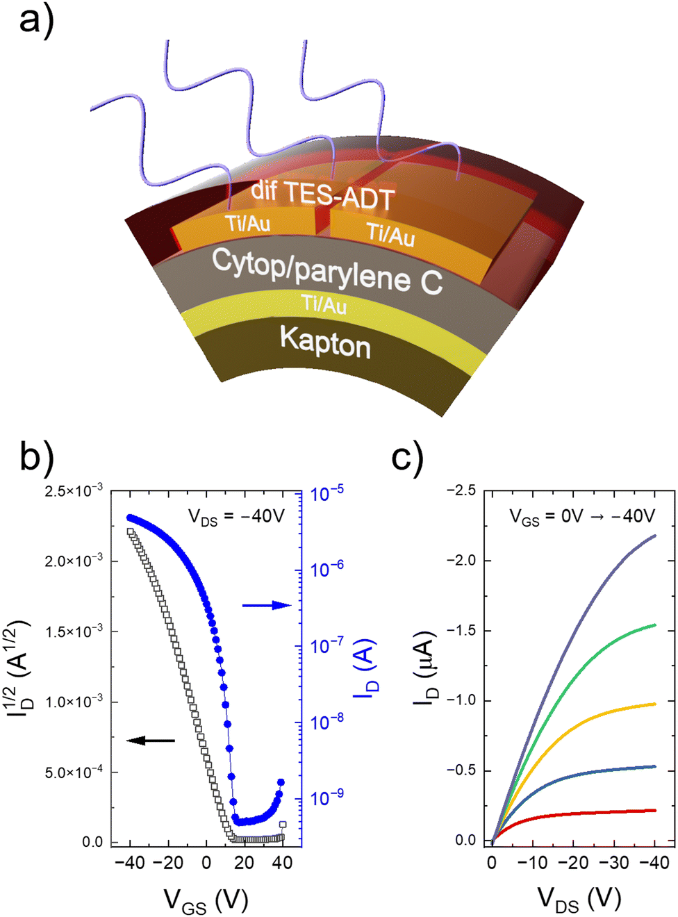 | ||
| Fig. 1 (a) BGBC device architecture of the RAD-OFETs. The substrate is Kapton with gold electrodes, the devices include a Cytop/parylene C double layer dielectric and diF-TES-ADT OSC. The source/drain contacts are treated with PFBT. (b) Typical transfer curve for a RAD-OFET immediately after fabrication. (c) Transport curve for a RAD-OFET device after fabrication. L/W = 30/400. | ||
RAD-OFET radiation exposure and characterization
The devices were characterised immediately after fabrication, as well as after radiation exposure in increment doses of 1 Gy (1 Gy = 1 J kg−1). Transistor characteristics were measured with a Keithley 2614b and SweepMe! (sweep-me.net) was used as the instrument control software. The scan rate was similar for all measurements and single voltage sweeps were acquired to minimize the bias stress effects that would introduce additional effects and complicate the analysis. The 6 MeV X-ray radiation exposures were performed at Wake Forest University Baptist Medical Center with an Elekta Versa HD linear accelerator configured with a 10 × 10 cm2 field size, 100 cm source-to-surface distance, 6 cGy s−1 maximum dose rate, and 1.5 cm solid water (Sun Nuclear Wisconsin, Middleton, WI) between the sample and accelerator. Similar samples, but which have not been exposed, have been tested as reference to distinguish environmental/aging effects from the radiation induced effects. At least ten devices of each type have been included in the average calculation.Trap density of states (t-DOS) analysis
Trap DOS analysis was carried out via the Grünewald method.12,17–21 The flat-band voltage (VFB) was assumed to be the turn on voltage extracted from the transistor transfer curve in the linear regime (more details in ESI†). The derivative steps of the computation were calculated using forward automatic differentiation via the Julia programming language to eliminate the rounding and truncation error from numerical differentiation.Photoluminescence spectroscopy
The diF-TES-ADT samples were kept in a closed cycle cryostat (Montana Instruments) and photo-excited with ∼220 fs pulses at 440 nm and at 2.5 mW power. The laser was a Yb:KGW amplifier (Pharos from Light Conversion), whose output at 1030 nm was converted to pulses at 440 nm using an optical parametric amplifier (Orpheus). The photoluminescence from the sample was fiber-coupled into a spectrometer (OceanOptics Maya). The temperature of the sample was scanned from 295 K to 15 K, while recording spectra at each 5 K interval.Structural studies
Grazing-incidence wide-angle X-ray scattering measurements were performed at the NCD-SWEET beamline (BL11), at ALBA synchrotron (Barcelona, Spain). We used a focused, collimated beam at 12.4 keV. The size of the beam was characterized as 50 × 50 microns. For data collection, we used a LX255-HS detector (Rayonix), placed at a distance of 210 mm from the sample holder. The samples were exposed to the beam for 1 second, at an incident angle between 0.08 and 0.2°. 10 frames were collected per angle to increase the signal-to-noise ratio.Results and discussion
Fig. 1(b) and (c) depict transfer and output curves measured on a typical RAD-OFET device before exposure to radiation. The dependence of the current–voltage curves on the radiation exposure is shown in Fig. S1 (ESI†), while in Fig. S2 (ESI†) we include the transfer curves of a reference sample that has been subjected to the same handling but has not been exposed to radiation. In both cases the drain current ID is significantly larger than the gate current IG, confirming that the leakage currents have minimal impact on the device operation. The threshold voltage, Vth, was extracted from the x-intercept of a linear fit of the square root of the drain current (black points, Fig. 1(b)) within the on-regime of the transfer curve, while the subthreshold slope, S, was extracted from the inverse slope of the log of the drain current at the turn on voltage (blue line, Fig. 1(b)). Fig. 2(a) shows the shift in the threshold voltage due to interaction with radiation, corrected for the environmental/aging effects, i.e. ΔVth = VthD − Vth0 where VthD is the average threshold voltage of RAD-OFETs exposed to radiation and Vth0 is the average threshold voltage of the reference devices. Ten devices of each type have been measured and the reported values represent the averages. Fig. 2(b) shows the average subthreshold slope S for control devices (red) and the RAD-OFETs exposed to radiation (blue), respectively. The control devices only exhibit a small increase in subthreshold slope, as typically expected from device aging, while the exposed RAD-OFETs exhibit a more prominent increase, suggesting that additional trapping states are created as a result of radiation exposure. The increase in the threshold voltage shift and subthreshold slope suggests that additional traps form within the organic semiconductor upon exposure to radiation. The density of interfacial trap states, NSit, can be estimated from the subthreshold slope (details included in the ESI†).18,22 Comparing the value determined at the maximum dosage to that before exposure, the difference provides the value of the radiation-induced interfacial trap density NSit = 9 × 10¹² eV−1 cm−2.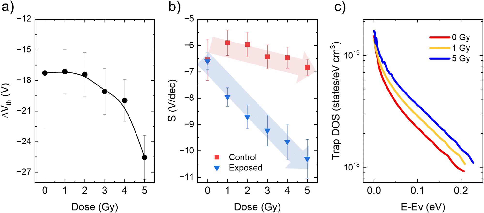 | ||
| Fig. 2 (a) The average shift in threshold voltage where the threshold voltage shift is the threshold voltage of a RAD-OFET subtracted by the threshold voltage of a control device. (b) The average subthreshold slope of the control devices and exposed RAD-OFETs. (c) The trap density of states for a RAD-OFET device at different dose exposures. | ||
To better understand the energetic distribution of the electronic trap states generated during irradiation, we performed t-DOS analysis on our RAD-OFETs as a function of exposure. These measurements provide a quantitative picture of the density and spectral distribution of the electronic trap states generated upon interaction with the X-rays. The spectral density of trap states was determined by analysing the transistor curves, and hence it reflects the properties of the semiconductor film at the interface with the dielectric layer, where the transistor channel forms. Nevertheless, given that the X-ray absorption length is significantly larger compared to the thickness of our films, the presence of a uniform defect density is a reasonable assumption. Fig. 2(c) shows the t-DOS of a RAD-OFET in the pristine sample and in the same device after that has been subjected to exposure to two different dosages of radiation (complete data set is included in Fig. S3, ESI†). Here the x-axis represents the energy above the mobility edge, i.e., the shift in the energy E relative to the quasi-Fermi level at the dielectric/semiconductor interface (EV is the energy of the mobility edge of the valence band). The electronic states close to the band edges are considered shallow traps and small amounts of external energy can excite a charge carrier back into the band. The curves in Fig. 2(c) show an exponential decrease in the t-DOS further within the band gap, while the area under the curves represent the total trap density. The corresponding fitting parameters and resulting trap density are included in Table S1 (ESI†). As the radiation dose increases from 0 to 5 Gy, there is an increase in the density of trap states by about 3 × 1017 cm−3, with the greatest change occurring deeper within the band gap. For comparison, the OFETs that have not been exposed to X-rays show a negligible change in the t-DOS within the accuracy of our measurements, see Fig. S4 (ESI†), confirming that the traps generated in the irradiated samples result from the defects generated by the interaction between the radiation and the organic semiconductor layer. The constant t-DOS in the reference samples is also a signature of device environmental and operation stability during sample handling and testing. While the creation of electronic localized states is detrimental for charge transport since it leads to degradation in transistor properties, these changes can be exploited towards the development of sensing applications. Quantifying and understanding the nature of these traps, as well as the factors responsible for their generation, is essential. It has been shown that the interaction of X-rays with small molecule organic semiconductors does not generate chemical degradation of the crystals or polycrystalline films and that partial trap healing can be obtained upon thermal annealing.2,23 Hence, structural defects most likely represent the origin of electronic trap states arising from interaction between the organic semiconductor film and X-ray radiation. Local structural disorder induced by external stimuli represents a ubiquitous source of trap states in van der Waals bonded molecular crystals.18 In the following, we will focus on the signatures of such structural defects using complementary measurements.
Photoluminescence spectroscopy
An increase in the disorder in the molecular packing upon radiation exposure may explain the enhanced role of defects in charge carrier transport. Independent evidence for this can be obtained through the analysis of the photoluminescence spectra of these films. Linear optical spectra of molecular aggregates carry a wealth of information on molecular-scale dynamics that drive electronic processes.24 Absorption of a photon by the aggregate generates a strongly bound electron–hole pair, an exciton, which is generally delocalized over several molecular units. The extent of delocalization is determined by the nature and magnitude of intermolecular coupling and is limited by the static and dynamic disorder.24 This information is embedded in the characteristic spectral lineshape obtained either via absorption or photoluminescence measurements.For example, in an H-aggregate the transition from the excited state to the lowest lying vibrational level in the electronic ground state (00 state) is optically forbidden, while in a J-aggregate it is the dominant transition.25 This condition however can get relaxed due to disorder-induced effects and accordingly, Spano has demonstrated that the ratio between the 0–0 and 0–1 peaks in the PL spectrum can be quantitatively linked to the coherence length of the exciton.24,26 In the case of a H-aggregate, substantial emission from the forbidden 0–0 transition can be observed due to thermal activation to the top of the exciton band and it is very sensitive to disorder.27 The 0–1 transition however is considerably insensitive to disorder. Accordingly, the temperature dependence of the ratio of their respective intensities I0–0/I0–1 is a measure of the disorder in the system. The ratio follows an Arrhenius-like activation behaviour ∼exp(−Δ/kT), where Δ is the activation energy and a higher Δ signifies enhanced disorder and increased exciton bandwidth.28
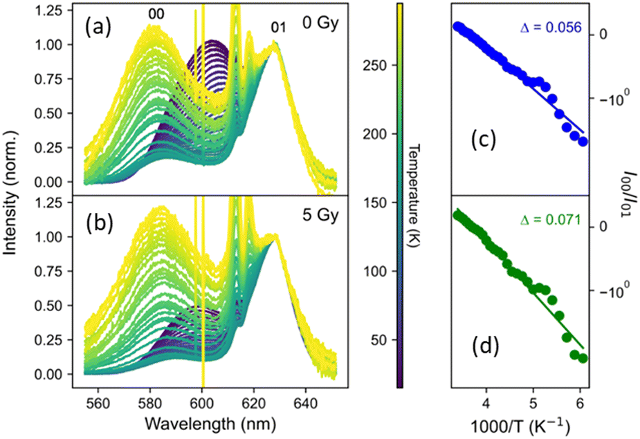
With this background, we performed temperature dependent photoluminescence measurements on films of diF-TES-ADT fabricated similarly to those used in RAD-OFETs, with and without the radiation exposure. Details of the measurement can be found in the Experimental section. Shown in Fig. 3(a) and (b) are the PL spectra of non-radiated and irradiated (5 Gy) samples, in the temperature range between 5 K and room temperature. We observe two clear peaks in the measured spectral range at 580 nm and 625 nm, which are assigned to the 0–0 and 0–1 transitions respectively. The additional narrower peaks are experimental artifacts from the spectrometer and can be ignored. We see a clear variation in the relative intensity of the two peaks and a complete quenching of the 0–0 transition at around 120–150 K in both samples, as well as a red shift in the PL spectral below this temperature, which was previously assigned to the emission from the triplet-pair. Here, we focus on the temperature dependence of the ratio I0–0/I0–1 associated with the singlet state emission above 120 K. As can be seen in Fig. 3(c) and (d) the ratio reduces with lowering temperature and the trend can be fitted to Arrhenius like activation to obtain an activation energy Δ of about 56 ± 2 meV for unexposed samples. This value approximately matches with the value obtained previously by Platt et al.28 Notably, we observe that the activation energy increases to about 71 ± 3 meV in the irradiated samples, indicating an increase in the disorder. While we acknowledge that the change is rather moderate and may be subject to experimental error, lower dosages will in fact result in changes that may not be experimentally accessible to linear spectroscopies owing to the uncertainty in the peak positions due to large inhomogeneous broadening. On the other hand, going to higher dosages to induce larger discernible changes would challenge the material robustness. However, we highlight that these measurements, seen in the context of other characterization techniques presented in this manuscript, can be considered to be real and representative of the modulation induced by the radiation.
 | ||
| Fig. 3 Temperature-dependent photoluminescence spectra of (a) unexposed and (b) exposed samples with a radiation dosage of 5 Gy. (c) and (d) Experimental data and fits of the temperature dependence of the ratio I0–0/I0–1 for un-irradiated and irradiated samples respectively. | ||
Structural studies
To identify the nature of the structural defects induced by the X-ray exposure, we performed grazing-incidence scattering measurements on films previously exposed to 2, and 5 Gy, respectively, and on the pristine film as a control sample. The GIWAXS patterns reveal several dot-like peaks, characteristic of highly crystalline, oriented materials. A broad halo, coming from the silicon oxide layer, is also visible. The reflections are consistent with the diF-TES-ADT triclinic lattice,29 in which the system consists of a layered structure of π stacked molecules. The most intense reflection, vertically oriented at q ≈ 3.8 nm−1 (d ≈ 16.4 nm) is highlighted in Fig. 4; it is associated with the layer spacing and is indexed as (001). While at first glance the GIWAXS patterns look equivalent, we have proven that increasing the X-ray doses on the film induces the growth of a second peak in the (001) region, slightly shifted towards higher q. The growing of a second peak can be explained as a distortion/rearrangement of the original crystalline lattice. This peak appears to be present, although much weaker, in the non-exposed sample, which means that a slight distortion is induced during the sample deposition or due to aging effects. This hypothesis is in line with the work performed on other small molecule organic semiconductors exposed to radiation, where similar effects have been explained based on the idea that the flux of X-ray photons disrupts the atomic lattice by detaching hydrogen atoms from the molecules.2,23,30 The hydrogen defects cause a strain on the lattice that induces a rearrangement of the global crystalline structure, and hence explains the increase of trap states. This increase, in the same way as with rubrene crystals,23 would have a structural origin. Apart from this hypothesis, we want to highlight the similarities between these results and the two peaks associated to two different polymorphs in this molecule.31 While both effects may take place, we think that the gradual growing of the shifted peak after increasing X-ray doses is coherent with an irreversible distortion of the original polymorph. Further analysis using complementary techniques to access the trap states is necessary to clarify the exact nature of the newly formed states.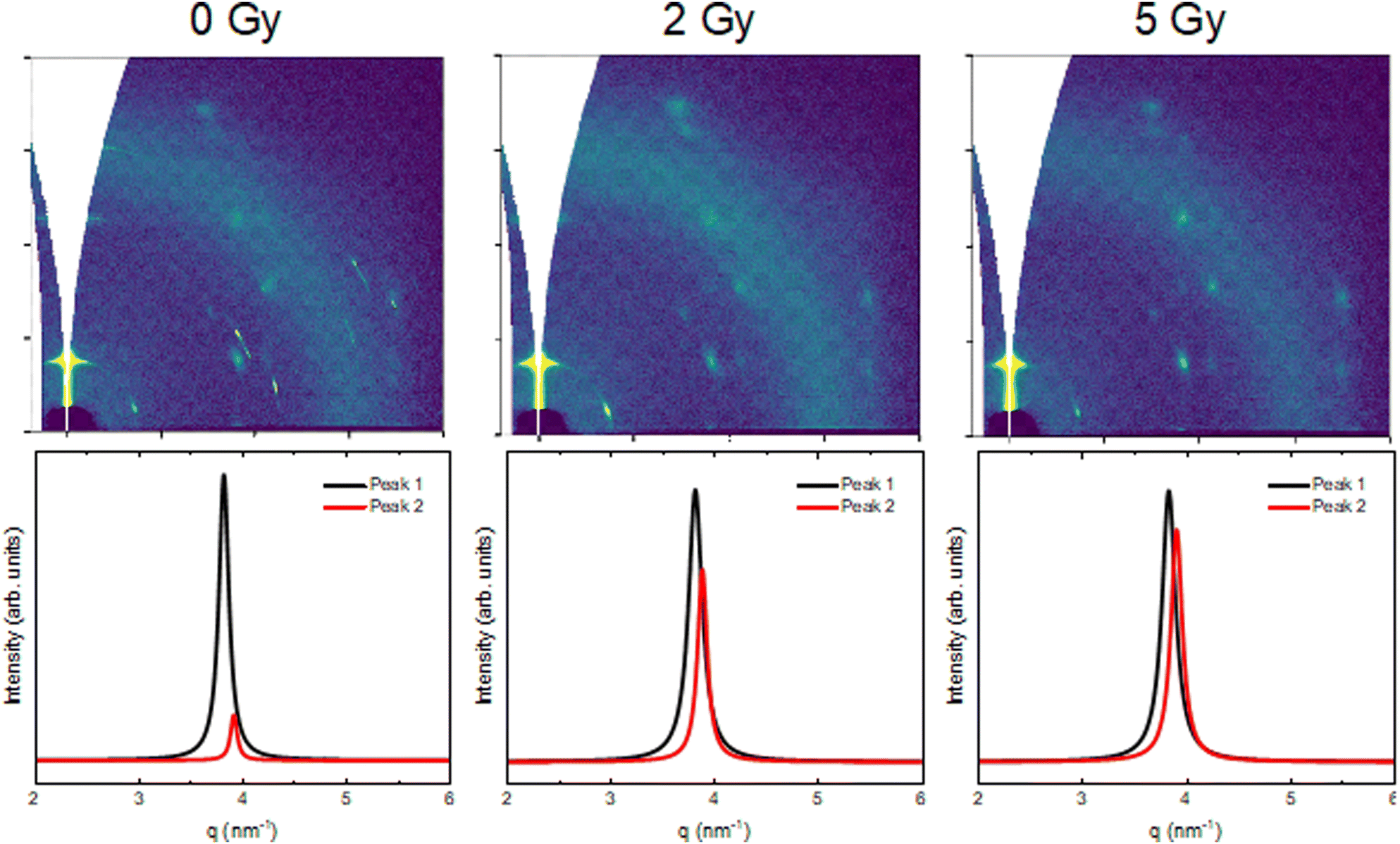 | ||
| Fig. 4 Upper row: GIWAXS patterns from non-exposed and two exposed films. Bottom row: deconvoluted Lorentzian peaks from the main reflection (001) of GIWAXS patterns. | ||
It is worth noting that the doses explored in our work are relevant for a wide range of applications, from exposure monitoring and worker safety to national security and medical applications. In medicine, for example (CT) scans require doses of 10−2 Gy, while during radiation therapy for cancer treatment a localized dose escalation is needed with 2–10 Gy prescribed at each treatment, with ∼40–60 Gy total given over several weeks, as indicated for an individual patient through our understanding of radiation dose fractionation.32,33 In special cases where the therapeutic goal is ablative, such as trigeminal neuralgia treatment, the delivered dose can be 90 Gy in a single treatment.34 The spectral signature (i.e., energy distribution) of the induced traps, combined with the evidence from optical and structural studies, collectively points to the formation of local structural disorder as the underlying cause of the emergence of new electronic states. This hypothesis for the microscopic origin of the trap states is also supported by the reduction in the t-DOS upon thermal annealing.2 Molecular re-arrangements driven by strain have been previously observed in van der Waals bonded systems and have been attributed to either growth-induced defects,35 or mismatched in the coefficients of thermal expansion of consecutive device layers.36 Strain can profoundly influence the properties of organic semiconductors, from altering the energetic landscape to suppressing molecular vibrations, or triggering phase transitions.37–40 It is important to highlight that the effects recorded in our work are different than those observed in similar molecular crystals upon exposure to proton or helium ion radiation, where t-DOS exhibited a peak around 0.3 eV above the mobility edge, which has been attributed to the formation of deep trapping states resulting from cleaving of the C–H bond followed by hydrogen detachment and repositioning.41 Such mobile chemical entities profoundly perturb the crystal environment and alter the space charge generated during device operation. The absence of a peak in the t-DOS spectrum, coupled with the lack of any discernible signature of impurity formation within the resolution of our measurements,2 implies that the electronically active states induced by radiation exposure are associated with structural disorder related to changes in molecular packing. Future studies utilizing local probe techniques will elucidate the spatial distribution and temporal evolution of these defects.
Understanding the processes occurring during the interaction of organic semiconductors with various radiation types, as well as the radiation-induced defects generated by this interaction, has implications on several other research areas. For example, scintillators based on organic materials are studied for direct X-ray detection through the photoconductivity effect.42 The formation of electronic traps can affect the scintillation process by reducing the number of photons emitted, resulting in a lower scintillation yield, and by slowing down the scintillation decay time. The random trapping and detrapping of charge carriers can also create fluctuations in the scintillation signal, making it difficult to detect weak scintillation events or to resolve the energy of incident radiation. Furthermore, the burgeoning field of organic devices for renewable energy and space applications calls for the development of radiation-stable materials, as these devices will operate in an environment of continuous natural background radiation.30
Conclusions
In conclusion, we have investigated the effects of radiation exposure on the electrical, structural, and optical properties of small molecule organic semiconductors subjected to controlled doses of X-ray radiation. We found that electronic trap states form upon exposure, and that the density of trap states correlates positively with dose. The presence of electronic traps induces shifts in the threshold voltage and an increase in the subthreshold slope of RAD-OFETs. Spectral analysis of the trap density of states (trap-DOS) clarified the energetic distribution of these new states, while grazing-incidence wide-angle X-ray scattering, and photoluminescence spectroscopy measurements revealed that the trap states arise from local structural disorder in the crystalline films. Our results provide a deeper understanding of the mechanism for radiation detection in organic dosimeters, which is a critical step towards fully exploiting the potential of organic semiconductors in radiation dosimetry and for designing higher sensitivity devices.Author contributions
D. D. fabricated all samples, characterized RAD-OFET devices, investigated the trap density of states, wrote manuscript. E. J. K. performed photoluminescence spectroscopy measurements, wrote manuscript. K. J. T. synthesized the organic semiconductor. E. G.-F. measured and analysed GIWAXS data, wrote manuscript. J. D. V. and J. D. B. performed the radiation exposures. J. E. A. edited manuscript. A. R. S. K. analysed PL data wrote the manuscript. O. D. J. coordinated the project, wrote manuscript.Conflicts of interest
There are no conflicts to declare.Acknowledgements
The work at Wake Forest University was supported by the National Science foundation through grant DMR-1627925, and at the University of Kentucky through grant DMR-1627428.Notes and references
- I. Temiño, L. Basiricò, I. Fratelli, A. Tamayo, A. Ciavatti, M. Mas-Torrent and B. Fraboni, Nat. Commun., 2020, 11, 2136 CrossRef.
- A. M. Zeidell, T. Ren, D. S. Filston, H. F. Iqbal, E. Holland, J. D. Bourland, J. E. Anthony and O. D. Jurchescu, Adv. Sci., 2020, 7, 2001522 CrossRef CAS PubMed.
- I. Fratelli, L. Basiricò, A. Ciavatti, Z. A. Lamport, J. E. Anthony, I. Kymissis and B. Fraboni, Adv. Mater. Technol., 2023, 8, 2200769 CrossRef CAS.
- A. C. Arias, J. D. MacKenzie, I. McCulloch, J. Rivnay and A. Salleo, Chem. Rev., 2010, 110, 3–24 CrossRef CAS PubMed.
- J. Rivnay, R. M. Owens and G. G. Malliaras, Chem. Mater., 2014, 26, 679–685 CrossRef CAS.
- A. Savva, A. Hama, G. Herrera-López, T. Schmidt, L. Migliaccio, N. Steiner, M. Kawan, H. Fiumelli, P. J. Magistretti, I. McCulloch, D. Baran, N. Gasparini, R. Schindl, E. D. Głowacki and S. Inal, Adv. Sci., 2023, 2300473 CrossRef CAS.
- Z. Peng, N. Stingelin, H. Ade and J. J. Michels, Nat. Rev. Mater., 2023, 8, 439–455 CrossRef.
- B. Fraboni, A. Fraleoni-Morgera and N. Zaitseva, Adv. Funct. Mater., 2016, 26, 2276–2291 CrossRef CAS.
- J. A. Posar, J. Davis, O. Brace, P. Sellin, M. J. Griffith, O. Dhez, D. Wilkinson, M. L. F. Lerch, A. Rosenfeld and M. Petasecca, Phys. Imaging Radiat. Oncol., 2020, 14, 48–52 CrossRef PubMed.
- L. Basiricò, A. Ciavatti and B. Fraboni, Adv. Mater. Technol., 2021, 6, 2000475 CrossRef.
- A. Tamayo, I. Fratelli, A. Ciavatti, C. Martínez-Domingo, P. Branchini, E. Colantoni, S. De Rosa, L. Tortora, A. Contillo, R. Santiago, S. T. Bromley, B. Fraboni, M. Mas-Torrent and L. Basiricò, Adv. Electron. Mater., 2022, 8, 2200293 CrossRef CAS.
- H. F. Iqbal, Q. Ai, K. J. Thorley, H. Chen, I. McCulloch, C. Risko, J. E. Anthony and O. D. Jurchescu, Nat. Commun., 2021, 12, 2352 CrossRef CAS PubMed.
- J. W. Ward, M. A. Loth, R. J. Kline, M. Coll, C. Ocal, J. E. Anthony and O. D. Jurchescu, J. Mater. Chem., 2012, 22, 19047–19053 RSC.
- J. W. Ward, R. Li, A. Obaid, M. M. Payne, D.-M. Smilgies, J. E. Anthony, A. Amassian and O. D. Jurchescu, Adv. Funct. Mater., 2014, 24, 5052–5058 CrossRef CAS.
- S. Anand, K. P. Goetz, Z. A. Lamport, A. M. Zeidell and O. D. Jurchescu, Appl. Phys. Lett., 2019, 115, 073301 CrossRef.
- D. J. Gundlach, J. E. Royer, S. K. Park, S. Subramanian, O. D. Jurchescu, B. H. Hamadani, A. J. Moad, R. J. Kline, L. C. Teague, O. Kirillov, C. A. Richter, J. G. Kushmerick, L. J. Richter, S. R. Parkin, T. N. Jackson and J. E. Anthony, Nat. Mater., 2008, 7, 216–221 CrossRef CAS.
- M. Grünewald, P. Thomas and D. Würtz, Phys. Status Solidi B, 1980, 100, K139–K143 CrossRef.
- H. F. Haneef, A. M. Zeidell and O. D. Jurchescu, J. Mater. Chem. C, 2020, 8, 759–787 RSC.
- I. Dobryden, V. V. Korolkov, V. Lemaur, M. Waldrip, H.-I. Un, D. Simatos, L. J. Spalek, O. D. Jurchescu, Y. Olivier, P. M. Claesson and D. Venkateshvaran, Nat. Commun., 2022, 13, 3076 CrossRef CAS PubMed.
- A. F. Paterson, Y.-H. Lin, A. D. Mottram, Z. Fei, M. R. Niazi, A. R. Kirmani, A. Amassian, O. Solomeshch, N. Tessler, M. Heeney and T. D. Anthopoulos, Adv. Electron. Mater., 2018, 4, 1700464 CrossRef.
- M. Geiger, L. Schwarz, U. Zschieschang, D. Manske, J. Pflaum, J. Weis, H. Klauk and R. T. Weitz, Phys. Rev. Appl., 2018, 10, 044023 CrossRef CAS.
- H. Klauk, Chem. Soc. Rev., 2010, 39, 2643–2666 RSC.
- T. Morf, T. Zimmerling, S. Haas and B. Batlogg, arXiv, 2016, preprint, arXiv.1303.3831 DOI:10.48550/arXiv.1303.3831.
- F. C. Spano, Acc. Chem. Res., 2010, 43, 429–439 CrossRef CAS PubMed.
- G. Lanzani, Photophysics of Molecular Materials: From Single Molecules to Single Crystals, John Wiley & Sons, Inc., 2006 Search PubMed.
- F. C. Spano, J. Clark, C. Silva and R. H. Friend, J. Chem. Phys., 2009, 130, 074904 CrossRef.
- F. C. Spano, J. Chem. Phys., 2005, 122, 234701 CrossRef.
- A. D. Platt, M. J. Kendrick, M. Loth, J. E. Anthony and O. Ostroverkhova, Phys. Rev. B: Condens. Matter Mater. Phys., 2011, 84, 235209 CrossRef.
- O. D. Jurchescu, S. Subramanian, R. J. Kline, S. D. Hudson, J. E. Anthony, T. N. Jackson and D. J. Gundlach, Chem. Mater., 2008, 20, 6733–6737 CrossRef CAS.
- L. Basiricò, A. F. Basile, P. Cosseddu, S. Gerardin, T. Cramer, M. Bagatin, A. Ciavatti, A. Paccagnella, A. Bonfiglio and B. Fraboni, ACS Appl. Mater. Interfaces, 2017, 9, 35150–35158 CrossRef.
- O. D. Jurchescu, D. A. Mourey, S. Subramanian, S. R. Parkin, B. M. Vogel, J. E. Anthony, T. N. Jackson and D. J. Gundlach, Phys. Rev. B: Condens. Matter Mater. Phys., 2009, 80, 085201 CrossRef.
- H. D. Thames, Semin. Radiat. Oncol., 1992, 2, 3–9 CrossRef.
- B. Emami, J. Lyman, A. Brown, L. Cola, M. Goitein, J. E. Munzenrider, B. Shank, L. J. Solin and M. Wesson, Int. J. Radiat. Oncol., Biol., Phys., 1991, 21, 109–122 CrossRef CAS.
- M. D. Chan, E. G. Shaw and S. B. Tatter, Neurosurg. Clin. N. Am., 2013, 24, 613–621 CrossRef PubMed.
- P. J. Diemer, C. R. Lyle, Y. Mei, C. Sutton, M. M. Payne, J. E. Anthony, V. Coropceanu, J.-L. Brédas and O. D. Jurchescu, Adv. Mater., 2013, 25, 6956–6962 CrossRef CAS PubMed.
- Y. Mei, P. J. Diemer, M. R. Niazi, R. K. Hallani, K. Jarolimek, C. S. Day, C. Risko, J. E. Anthony, A. Amassian and O. D. Jurchescu, Proc. Natl. Acad. Sci. U. S. A., 2017, 114, E6739–E6748 CrossRef CAS PubMed.
- Y. Wu, A. R. Chew, G. A. Rojas, G. Sini, G. Haugstad, A. Belianinov, S. V. Kalinin, H. Li, C. Risko, J.-L. Brédas, A. Salleo and C. D. Frisbie, Nat. Commun., 2016, 7, 10270 CrossRef CAS PubMed.
- T. Kubo, R. Häusermann, J. Tsurumi, J. Soeda, Y. Okada, Y. Yamashita, N. Akamatsu, A. Shishido, C. Mitsui, T. Okamoto, S. Yanagisawa, H. Matsui and J. Takeya, Nat. Commun., 2016, 7, 11156 CrossRef CAS.
- G. Giri, R. Li, D.-M. Smilgies, E. Q. Li, Y. Diao, K. M. Lenn, M. Chiu, D. W. Lin, R. Allen, J. Reinspach, S. C. B. Mannsfeld, S. T. Thoroddsen, P. Clancy, Z. Bao and A. Amassian, Nat. Commun., 2014, 5, 3573 CrossRef CAS PubMed.
- C. Westermeier, A. Cernescu, S. Amarie, C. Liewald, F. Keilmann and B. Nickel, Nat. Commun., 2014, 5, 4101 CrossRef CAS.
- T. Zimmerling, K. Mattenberger, M. Döbeli, M. J. Simon and B. Batlogg, Phys. Rev. B: Condens. Matter Mater. Phys., 2012, 85, 134101 CrossRef.
- M. Koshimizu, Jpn. J. Appl. Phys., 2022, 62, 010503 CrossRef.
Footnote |
| † Electronic supplementary information (ESI) available. See DOI: https://doi.org/10.1039/d3mh01507f |
| This journal is © The Royal Society of Chemistry 2024 |