
 Open Access Article
 This Open Access Article is licensed under a
 Creative Commons Attribution 3.0 Unported Licence
Brain-inspired computing: can 2D materials bridge the gap between biological and artificial neural networks?
Deependra Kumar
Singh
*a and
Govind
Gupta
 *ab
*ab
aCSIR-National Physical Laboratory, Dr K. S. Krishnan Marg, New Delhi-110012, India. E-mail: deependrasingh92@gmail.com
bAcademy of Scientific & Innovative Research (AcSIR), Ghaziabad 201002, India. E-mail: govindnpl@gmail.com
First published on 7th March 2024
Abstract
This modern era of technology with data flood actively demands the development of excellent non-volatile storage (NVS) and computing devices, which can overcome the memory bottleneck of the traditional von-Neumann structure-based devices. Memristors, as potent and promising NVS devices, can efficiently mimic the biological synapse of a neuron, and therefore, have been immensely explored in recent years. In this context, the emergence and development of two-dimensional layered materials (2DLMs) have led to a multifold acceleration in the advancement of memory devices, owing to their atomically thin structures and superior electronic properties, in comparison to those of the conventional metal oxides. However, unlocking the full potential of 2DLMs in neuromorphic applications demands creative approaches. Here, we discuss in depth the challenges and limitations associated with these neuromorphic devices and finally conclude by outlining future perspectives and directions for this evolving field of next-generation electronics.
1. Introduction
In this modern digital world, data has become the new wealth.1,2 Complementary metal oxide semiconductor (CMOS) technology has achieved remarkable milestones, transforming the electronics landscape. Its low power consumption, high integration density, and reliability have revolutionized microelectronics. Innovations in CMOS technology have paved the way for development of smaller, faster, and more energy-efficient devices, such as microprocessors, memory chips, and sensors. This technology has played a pivotal role in the digital revolution, enabling the development of smartphones, computers, and advanced communication systems. Advancements in CMOS technology continue to drive progress in emerging fields like the Internet of Things (IoT), artificial intelligence (AI), and quantum computing, showcasing its enduring impact on diverse technological domains.3 One of the remarkable achievements is the development of FinFET (Fin Field-Effect Transistor) technology, which emerged as a breakthrough in CMOS design.3–5 This three-dimensional transistor structure helped overcome some of the limitations of traditional planar transistors, allowing for better control over current flow and reduced leakage, thereby enhancing performance and energy efficiency. CMOS technology has also enabled the integration of an entire system onto a single chip, leading to the development of System-on-Chip (SoC) designs. This integration has resulted in smaller, more compact, and power-efficient devices, ranging from smartphones to IoT devices.6 Another interesting area that the researchers are exploring is the use of quantum dots in transistors to push the limits of traditional CMOS technology. Quantum dot transistors have the potential to offer improved performance, energy efficiency, and novel functionalities compared to conventional transistors.7–9 However, as the CMOS-based devices continue to show a decrease in dimensions and reach their physical limits, the continuation of Moore's law faces tough challenges.10,11 Hence, innovative and efficient memory devices are being continuously explored to meet this rising demand.10 AI, neural networks, and machine learning have played a vital role in the recent development of memory and data storage devices.12 In conventional von Neumann computing devices, the processing and the memory units are different, and the mismatch of the speed between data fetching and processing leads to lower efficiency and higher power consumption, referred to as the von Neumann bottleneck.13 However, in contrast to the von Neumann architecture, the human brain comprises a network of billions of neurons and synapses for information storage and transfer.13 The brain can process and store multitudes of information simultaneously, thereby making the human brain the most advanced supercomputer that exists today. If the intelligence of the brain is mimicked in the state-of-the-art technology, next-generation energy efficient machines could be designed that can evolve and learn like the brain (Fig. 1). It has spurred tremendous research on devices that can mimic the functionality of biological neurons. Devices that exhibit resistive switching (RS) or memristive behavior have garnered the most attention due to their ability to be utilized as potential synaptic hardware systems while consuming very low energy, fulfilling the criteria of brain-inspired or neuromorphic computing.14–18 A memristor is a device proposed by Prof. Chua in 1971, considered as the ‘fourth fundamental non-linear circuit element’ relating charge with magnetic flux, and is characterized by a pinched hysteresis in its I–V curve.19 | ||
| Fig. 1 Schematic depicting the integration of the human brain with modern day processors to produce neuromorphic devices. | ||
The term “neuromorphic” was coined in the late 1980s by Carver Mead,20 who pioneered the development of neuromorphic silicon neuron circuits. Conventional electronic materials have played a major role in the early accomplishments of neuromorphic computing.21–26 For instance, Zhang et al.27 have implemented a robust machine-learning classifier in a standard 6T static RAM (SRAM) array. It is a prototype 128 × 128 SRAM array that has been applied in a 130 nm CMOS process. Frenkel et al.28 have introduced ODIN, an online-learning digital spiking neuromorphic processor, in a 28 nm fully depleted silicon on insulator CMOS that measures 0.086 mm2 and has 64 000 synapses, 256 neurons, and a minimum energy per synaptic operation of 12.7 pJ. Other well-known examples include the SpiNNaker Project,29 part of the European Union Human Brain Program, which can do cognitive tasks, and the TrueNorth chip from IBM, which can identify different objects from video feeds in real-time.30 The IBM's TrueNorth chip,31 which consists of 4096 cores and 5.4 billion transistors and integrates 1 million programmable spiking neurons and 256 million adjustable synapses, makes full use of the matured silicon technology and is a good choice for multi-object detection and classification. Another step forward in this direction was the development of the Loihi chip from Intel,32 which was unveiled in 2017. It features 128 neuromorphic cores, each of which contains 1024 basic spiking neural units arranged in tree-like architectures, for a total of over 131 thousand simulated neurons and nearly 130 million synapses. In contrast to the TrueNorth chip, the Loihi chip supports self-learning based on spiking neural networks in addition to inference. However, these CMOS-based devices may not be the eventual solutions for futuristic AI requirements, since these devices possess complex circuit topologies that consume a lot of power and require a large amount of chip area, in addition to the limitations in further scalability due to decline in the CMOS growth. Recently, two-dimensional (2D) materials have been actively deployed to fabricate various electronic and optoelectronic devices.33–42 Their high charge carrier mobility,43–45 band gap tunability,46 high light absorption coefficient,40,45 ease of heterojunction formation,47 and high surface-to-volume ratios48 make them promising candidates for realizing RS memory and other neuromorphic circuit elements.10,12,49 Furthermore, van der Waals (vdW) heterojunctions synthesized by stacking two or more 2D layered materials (2DLMs) not only retain the properties of the individual 2D materials, but also exhibit more intriguing properties than the respective counterparts.43 Recently, several 2DLMs and their heterostructures have been successfully utilized in memristive devices, for instance, graphene,50 layered metal chalcogenides,51,52 MXenes,53 and various other 2D materials.54 Wang et al.55 have discussed in detail the huge potential of 2DLMs in the development of low power and multifunctional neuromorphic devices, with respect to advancements in the device, chip and circuit levels. The rigorous efforts in the search for novel 2DLMs and their heterostructures along with the progress in their high-quality and wafer-scale growth have proven to be critical for exploiting memory devices with new operational mechanisms. Moreover, it is equally important to explore new architectures for neuromorphic devices, which could be crucial for enhancing the overall figures of merit of these devices. The authors have also discussed the unique properties of various 2DLMs, for instance, (i) the gate-tunable physical properties of 2DLMs enable the realization of diverse optoelectronic devices; (ii) the semimetallic nature of graphene and other transition metal dichalcogenides (TMDCs) makes them suitable for use as electrodes in these memory devices; (iii) effective suppression of operating current due to low density of states in graphene reduces energy consumption; (iv) 2DLMs exhibit much higher mechanical strength as compared to conventional metal oxides, which is crucial for achieving reliable resistive switching characteristics. Chiang et al.56 have also elucidated the utilization of 2DLMs in different memory devices based on their physical properties, such as ferroelectricity, ferromagnetism, phase change characteristics, filament formation, etc. In particular, they have emphasized the novel MoTe2-based resistive random-access memories (RRAMs), whose functionality depends upon the electric field-driven transition between two crystalline phases. Additionally, they have also provided an experimental demonstration of a proof-of-concept heterostructure made up of MoTe2 and WSe2 with appropriate properties for RRAM integration. However, relentless investigation still needs to be done so as to fully unveil the potential of these 2DLMs towards the realization and actualization of futuristic memory technologies.
Neural networks are designed utilizing two essential building blocks – neurons and synapses, as depicted in Fig. 2(a). The parallel connection of membrane capacitance (Cm) and membrane conductance (G) can be used to mimic the membrane of a biological neuron (Fig. 2(b)).13,57 When the membrane capacitance voltage crosses a threshold, the membrane conductance may undergo a change in its resistance, thus exhibiting multiple conductance states. Fig. 2(b) also depicts a synapse, which is the second essential neuromorphic building element. The synapse serves as a location for storage and modification of the input's weight (also known as the synaptic weight). These modifications are achieved by adjusting the concentration of neurotransmitters in synapses.13Fig. 2(c) shows the utilization of memristors in artificial neural circuits to emulate biological neurons and synapses. In the last few years, various reviews and perspectives have come up that have investigated this exciting field from the perspective of electrical properties of the devices, different materials for RS, device architectures, memristive synapses and the underlying mechanisms, external stimuli to achieve RS, etc.12,58,59 and concluded by providing a brief discussion of the challenges and outlook. However, a comprehensive discussion regarding the current hurdles in the field of brain-inspired computing is still lacking. Moreover, there is a huge need to shed light on the strategies to overcome these challenges for the fabrication of next-generation devices. Therefore, in this Perspective, we focus mainly on the challenges and limitations in the field of 2DLM-based neuromorphic devices reported to date, and discuss the plausible solutions for these challenges in terms of different growth techniques, design methods, utilization of novel materials such as phase change materials (PCMs), plasmonic metal nanoparticles, etc. We mainly highlight all the possible approaches and unexplored pathways to design highly efficient devices for this emerging research field.
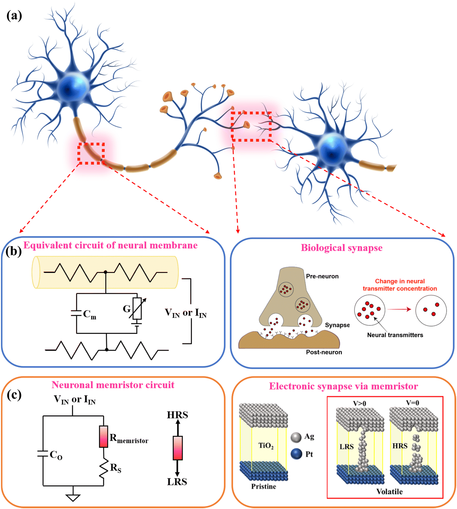 | ||
| Fig. 2 (a) Schematic depicting biological connectivity in neural organisms, showing the fundamental components i.e. a neuron and synapse. (b) Electrical model of the neural membrane; by adjusting the concentration of neuronal transmitters at the synapses, neural systems can exhibit adaptive behavior. Reproduced with permission from ref. 13 and 57. Reprinted with the permission of AIP Publishing; copyright 2018, Frontiers. (c) Equivalent electrical circuit utilizing a memristor to mimic the neural membrane; electronic memristor synapse structure (Ag/TiO2/Pt) that mimics a biological synapse. Reproduced with permission from ref. 13, 14 and 57. Reprinted with the permission of AIP Publishing; copyright 2023 and American Chemical Society; copyright 2018, Frontiers. | ||
2. Types of neuromorphic devices
Memristors encompass a wide range of electronic devices. They all carry out the fundamental functional concept of a memristor, despite using various structures, materials, and operating systems. Here, based on their structural differences, we divide the various memristors into two groups.2.1. Two-terminal devices
These can either have lateral or vertical architecture, involving a single active material or a heterojunction.60,61 Currently, the most popular types of memristors in this category are the cation- and anion-based ones. The input of these two-terminal memristors is typically a fixed voltage across the device; the synaptic weight of the device can be understood as its conductivity or the channel current at a fixed input voltage.62 The electric field causes anions or cations to migrate when a voltage is applied across the device, progressively forming filaments between the electrodes that alter the resistance. Oxygen vacancies are thought of as the migratory species in anion-based memristors, and oxides are typically utilized in their fabrication,62 such as TiO2,63 WO3,18etc. On the other hand, the metal cations from the electrodes form the filaments in cation-based memristors. In this instance, the active anode (Ag or Cu) and inert cathode in this memristor are typically separated by a solid electrolyte.64 Additional techniques for fabricating a two-terminal memristor have also been explored. For example, ferroelectric devices are subjected to electrical inputs that cause the ferroelectric materials to gradually polarize. By modifying the carriers' injection or tunneling, the degree of polarization influences the conductivity.65,66 Other types of memristors that have been researched are the spin-based ones; examples of these include spintronic and spin transfer torque magnetoresistive RAM memristors.67,68 The major ways to optimize two-terminal memristors are use of novel materials or modification of the existing ones by doping. Modifying the device's fabrication methods and/or structure is another way to optimize.622.2. Three-terminal devices or memtransistors
Memristive behavior can also be obtained using three-terminal devices, which are typically field effect transistors,69,70 and are usually vertical devices utilizing a single or hybrid active material. The input and output ports of a three-terminal device are dependent upon the testing setup, in contrast to the input/output ports of a device with two terminals, where these are the same since the voltage can only be produced by the two electrodes through which the current passes. A dielectric layer separates the gate from the source/drain and the channel in a three-terminal device, and so the only current passing through a memristor is the channel current.62 As a result, the source–drain port must be the output port. Conversely, the drain–source port or the gate-source/drain port can be used as the input port. In three-terminal memristors, the memristive function is often dependent on the gate terminals. Almost always, the gate voltage efficiently tunes the carrier activity by causing a gradual change in the channel area or the dielectric/channel interface. The fundamental needs of a memristor – conductivity tuning and memory – can be met if this change is long-lasting. For these devices, it is quite hard to discover a common optimization technique since different types of transistor-based memristors have distinct operating mechanisms behind the memristive functionalities.623. Different mechanisms of resistive switching
The basic principle behind any RS behavior is the existence of the active material in more than one interchangeable conductance states, which are termed a high resistance state (HRS) and low resistance state (LRS).4 The switching between these multiple conduction states upon the application of external stimuli, such as light, bias, pressure, temperature, etc., leads to the phenomenon of RS. Different mechanisms have been observed behind this reversible switching between the various conduction states, which have been reviewed here (Fig. 3).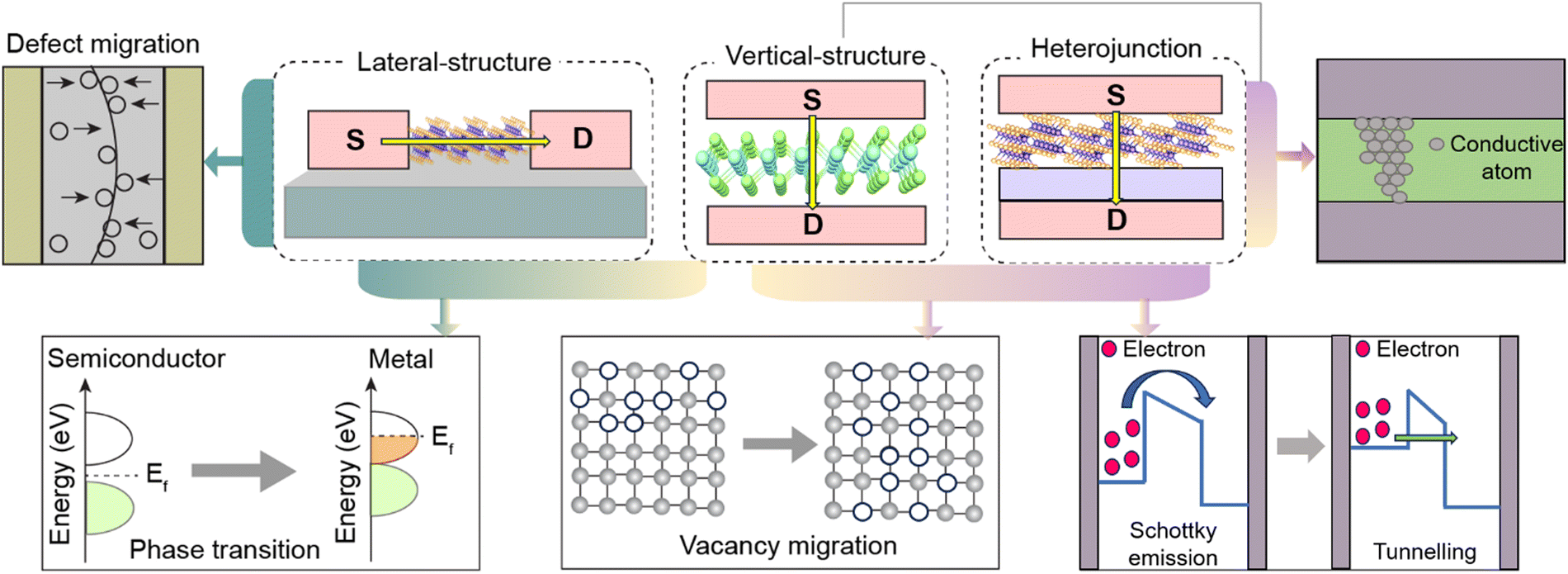 | ||
| Fig. 3 Schematic depicting common mechanisms of RS. Reproduced with permission from ref. 12. Copyright 2020, John Wiley & Sons, Inc. | ||
3.1. Defect migration along grain boundaries
This mechanism is generally found in devices with lateral architecture, where the defects present in the system move towards the grain boundary upon application of an external stimulus, thereby creating a low resistance path for conduction. For instance, Sangwan et al.71 have demonstrated a single layer MoS2-based lateral device where the accretion of the sulfur vacancies along the grain boundaries leads to the changes in the conductance of the MoS2 channel upon application of different biases, thereby causing memristive switching. Defect migration primarily occurs along grain boundaries due to the lower activation energy required for diffusion compared to migration through the bulk material. Grain boundaries provide energetically favorable pathways for defect migration, allowing defects to move and accumulate along these interfaces. These lateral memristors that make use of defect migration have the advantage of being able to produce multi-terminal and gate-tunable memristors, as well as eventually scaling a device down to atomic thickness. However, further requirements include carefully regulated defect engineering and lowering the operation voltage while maintaining a stable operation in devices in order to construct a memristor with the desired features.123.2. Phase change materials
Certain materials like VO2 undergo phase transitions between metallic (LRS) and semiconductor states (HRS)72–74 to exhibit neuromorphic properties. Similar to this unique feature of correlated oxides, several 2D materials such as MoS2, WTe2, MoTe2, TaS2, etc. have been stabilized in their low resistance phase (such as the metallic (1T) phase in MoS2),17,75 which can be reversibly switched to their high resistance phase (for instance, the hexagonal (2H) phase in MoS2). These kinds of phase transitions have been demonstrated both in vertical and lateral devices, usually by application of external bias. Cheng et al.17 have demonstrated an MoS2-vertical memory device with a simple metal–semiconductor–metal architecture. The active MoS2 layer contains 92.5% of the 1T phase and the remanent is the 2H phase. This 1T phase has an octahedral structure, and density functional theory calculations predict reversible semiconductor-to-metal transition in this phase owing to strong interactions between different orbitals. From the electrical measurements, the semiconductor-to-metal phase transitions occur at very low bias values, signifying the typical bipolar RS mechanism. Phase change memristors can switch between resistance states very quickly, on the order of nanoseconds to microseconds. This high-speed operation makes them suitable for applications where rapid switching is required, such as in memory and logic circuits. These memristors have also been exploited to realize neuronal memristor circuits, which mimic the behavior of neurons and generate action potentials,57 as depicted in the left panel of Fig. 2(b) and (c). Furthermore, these memristors typically exhibit good endurance and retention characteristics along with high scalability, allowing for high-density integration on semiconductor chips. However, certain disadvantages are also associated with the PCM-based memristors. When compared to other non-volatile memories, these memristors exhibit high RESET voltage, which is required to cause local heating sufficient for the material layer to undergo phase switching.76 Moreover, these devices are also associated with temperature sensitivity, which may impact the performance of the device. Variations in temperature might cause inadvertent resistance changes, which can affect the precision and consistency of data that are stored. There is also a change in the crystal structure linked to these phase transitions. Consequently, over time, mechanical wear and tear brought about by frequent structural transitions causes a decline in the device's performance.133.3. Conductive filament
This mechanism is mostly observed in the case of two-terminal devices, as discussed previously. Formation and rupture of conductive filaments is the most observed RS mechanism in vertical and lateral devices with the metal–semiconductor–metal or metal–insulator–metal configuration, where the active layer can be any oxide, a 2DLM, etc. In such configurations, a semiconducting film is sandwiched in between an active and an inert electrode. Ion-related migration and redox processes frequently result in the formation of localized conduction channels in the devices, and this process is aided by the external electric field. The migration of active metal ions is a significant subset of ionic effects. Conductive filaments in these memristors form and spontaneously rupture as a result of the active electrode materials (such as Ag or Cu), due to their limited thermodynamic stability and high diffusivity,77 being oxidized (X → Xn+ + ne−) and the generated cations migrating towards the inert electrode and being reduced (Xn+ + ne− → X).78 Therefore, the growth and dissolution of these conductive filaments realized by the electrochemical redox reactions taking place at each electrode/semiconductor junction and the subsequent transport of ions results into the RS behaviors. Such memristors have been recently utilized to achieve volatile switching behavior, emulating nociceptive behavior.14 Yin et al.79 have demonstrated an electrochemical metallization memory device based on the migration of Ag ions on the surface of 2D MoS2 to form conducting filaments comprising Ag NP chains of diameter ∼5 nm in its LRS. The biggest advantage of this mechanism is that a very large variety of materials can be used to obtain switching behavior, which makes it very promising for future applications. However, as already discussed, the device's low repeatability is caused by its inability to control the production and rupture of these nanofilaments, which has made it difficult to use the device in practical applications. Moreover, this mechanism is only possible in devices with relatively thin active layers; otherwise, a high power consumption is required for the formation of these conductive filaments. Another drawback is the formation of dead cells from these filaments, which can cause short circuits in devices.3.4. Vacancy formation and migration
Similar to the conducting filament-based memristors, the defects present in the system can form a vacancy-induced conductive filament (VICF) under application of an electric field, which results into the HLRS. Therefore, numerous families of compounds including oxides, sulfides, selenides, tellurides, etc. exhibit this mechanism, which gives it an upper hand for fabricating memristors. This mechanism is also analogous to the migration of defects along the grain boundaries, with the only difference being that these VICFs can be formed anywhere in the 2DLM layer, unlike the case where the defects line up along the grain boundaries. This mechanism is commonly observed in vertical devices with both metal-active layer-metal and heterojunction-based configurations. Devices dominated by ion transport appear to have superior retention performance, making them more attractive for applications like data storage.80 Such devices usually show digital RS, which has applications in RRAMs.60 Moreover, for applications involving data encryption and cybersecurity, the stochasticity in this switching behavior can be utilized as a real random number generator.81 Chen et al.82 reported a carbon-doped h-BN memristor, with a controlled number of defects induced by modulating the weight percentage of the carbon powder during synthesis. The defects in h-BN form a VICF when an electric field is applied, and the device exhibits bipolar NVS capability with low energy consumption along with a long retention time. Precise control over defect engineering becomes critical in such devices, which determines the performance of these memristors. Randomness in the formation of vacancy filaments, which leads to cycle-to-cycle and device-to-device variations, is one of the key issues that needs to be addressed in order to realize efficient, reliable and practical devices.3.5. Modulation of Schottky emission
Another interesting mechanism in memristive devices is the reversible transition of the carrier transport between Schottky emission and other mechanisms, such as direct tunneling, Ohmic conduction, etc.60 The alteration in the Schottky barrier height of the metal/semiconductor contact or the heterojunction is the key for RS. The continuous tunability of the resistive state is the most crucial aspect of the device in these cases, and hence electron-transport-dominated devices are significant for electrically simulating synaptic properties or learning/memory behaviors.80 Type-II heterojunctions, which can be transformed into type-III heterojunctions, can potentially change their conduction mechanism from Schottky emission to tunneling.47 The advantage of such memristors is that the thickness of the active layer can be reduced to the sub-nanometer range, without being affected by the leakage current due to atomic defects. However, higher energy required to alter the barrier height poses limitations on such memristors. Moreover, obtaining significant modulation in the barrier height is very crucial to achieve an appreciable HRS/LRS ratio. In 2018, Ge et al.83 reported a stable non-volatile atomristor based on the Au–MoS2–Au vertical device, showing RS. The device exhibited the HRS in the Schottky emission transport and the LRS when the carrier transport transitioned to direct tunneling.4. Common terminology in neuromorphic computing
By exploiting suitable mechanisms discussed above, the performance of memristors can be modulated and enhanced. The performance can be evaluated through various critical parameters that determine their behavior. These parameters play a crucial role in understanding and designing memristor-based devices for specific applications. Some of the key critical parameters of memristors have been defined and are summarized in Fig. 4 and the common terminologies related to neuromorphic computing are summarized as follows: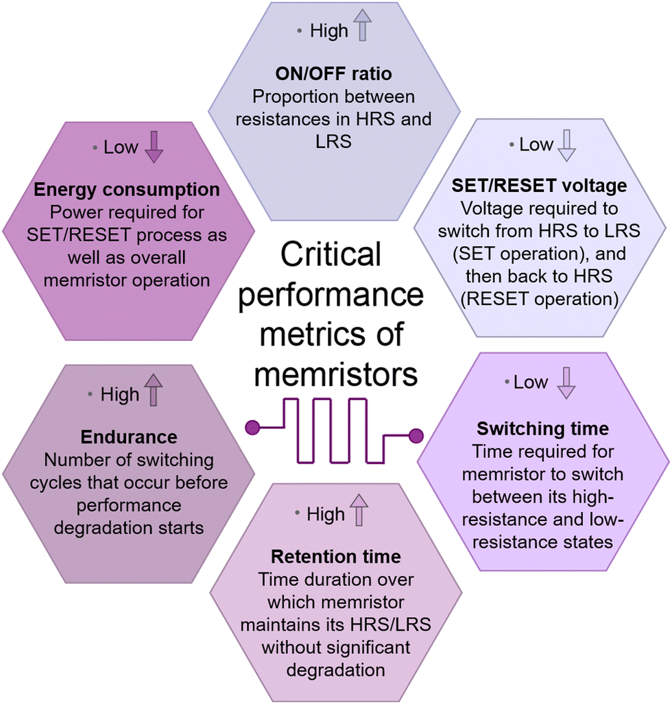 | ||
| Fig. 4 Critical parameters for evaluation of the performance of memristors. | ||
4.1 Neurons
Neurons are the basic building blocks of the nervous system and brain, which receive sensory information from the outside environment and are responsible for sending motor commands to our muscles, and converting and relaying electrical signals at each stage.4.2 Synapses
Synapses are the junctions between two neurons, which transmit information between these two neurons in the form of electrical and chemical signals.4.3 Synaptic weight or synaptic plasticity
Synaptic weight or synaptic plasticity refers to the amplitude or strength of a connection between two neurons.4.4 Spike timing dependent plasticity
Spike timing dependent plasticity is the process that alters the strength of the connection between two neurons, which is based upon the relative timing of the input and output action potentials of a particular neuron.4.5 Spike rate dependent plasticity
Spike rate dependent plasticity involves the modulation of synaptic plasticity based on the average firing rate or the firing frequency of the action potentials.4.6 Short term memory (STM)
Short term memory (STM) involves the gradual increase of the synaptic weight, which persists for a short period of time (a few seconds or minutes).4.7 Long term memory (LTM)
Triggering the STM repeatedly results into a long-lasting modification of the synaptic plasticity, which can last for months or years, and sometimes indefinitely.4.8 Long term potentiation
Long term potentiation is the procedure that involves consistent synaptic strengthening, resulting into an increase in the signal transmission between neurons over time.4.9 Long term depression
Long term depression is the process through which synapses lose some of their efficacy to transmit neural signals.4.10 Non-volatile storage (NVS)
Non-volatile storage (NVS) is a memory that retains the stored data for a long time, even after the power is turned off.4.11 Volatile memory
Volatile memory is memory that can retain the data for short time periods, only up to the time it gets a power supply.4.12 Paired-pulse facilitation (PPF)
Paired-pulse facilitation (PPF) refers to the typical change in the short-term synaptic weight controlled by the temporal relationship between the two consecutive presynaptic electrical spikes. For instance, if two successive presynaptic action potentials occur at the presynaptic terminal having a time interval (Δt), then PPF is defined as the ratio of the postsynaptic currents because of the second spike (I2) and first spike (I1), that is, PPF = I2/I1.5. Roadmap of memristive and neuromorphic devices
A brief timeline of some of the major milestones achieved in the field of neuromorphic computing is shown in Fig. 5. After the theoretical prediction of a memristor by Chua et al.19 in 1971, immense efforts have been made to implement it in an electrical circuit. A few decades later, in 2008, Strukov et al.63 from Hewlett–Packard Laboratories first revealed that memristive behavior can be experimentally realized in a real device utilizing the Pt/TiO2/Pt structure. The migration of oxygen vacancies in the TiOx layer, which caused the gradient change of the doping state, is responsible for the observed memristive switching characteristics. The initial application of synthetic synapses made of carbon nanotubes was first shown in 2013 by Gacem et al.84 Two years later, the first report on a 2DLM-based memristor was published by Sangwan et al.,71 in which an MoS2 monolayer-based field effect transistor was utilized. The RS behavior in the three terminal device was attributed to the geometry of the grain boundaries present in the MoS2 layer. Zhao et al.85 in 2017 investigated the resistive switching of conductive filaments in a material medium with a sub-nanometer thickness for the first time. The oxidation of 2D hexagonal boron nitride (h-BN) was employed, which created an atomically thin switching medium layer. The resulting memristor device can function at femtojoule level energy usage per bit, sub-picoampere on-state current, and less than 1 V working voltage. Later, Wang et al.86 demonstrated a vdW heterostructure utilizing graphene/MoS2−xOx/graphene with superior thermal stability. With an endurance of up to 107 cycles and a high operating temperature of 340 °C, the device exhibited exceptional switching capability. The high thermal stability has been attributed to the MoS2−xOx switching layer, the graphene electrodes, and the atomically sharp interface between the electrodes and the switching layer. Yan et al.87 have shown that 2D WS2 with a 2H phase can produce high-performance memristors with low power consumption, which exhibit quick ON and OFF switching times of 13 and 14 ns, respectively, along with a low program current of 1 A in the ON state, and SET/RESET energy is on the order of femtojoules. It was revealed that the creation of sulfur and tungsten vacancies and electron hopping between vacancies are the most possible mechanisms responsible for the enhanced RS performance. Memristor crossbar arrays based on h-BN have been demonstrated by Chen et al.88 with high yield (98%), low device-to-device variability (5.74%), and low cycling tolerance variability (1.53%). The Ag/h-BN/Ag device exhibited a very high ON/OFF ratio of up to 1011 and an extremely low SET energy consumption of 8.8 zJ. Subsequently in 2021, with the help of electron-beam irradiation, a Ti/PdSe2/Au memristor was demonstrated, which was able to show a long retention duration of up to 105 s.89 The production of conductive filaments can occur in channels created by the grain boundaries produced by electron-beam irradiation, which enables the memristor to display the distinct quasi-reset RS characteristics. In 2022, Li et al.90 demonstrated a memristor crossbar array utilizing polycrystalline HfSe2 grown by molecular beam epitaxy on a 2-inch wafer, followed by a metal-assisted vdW transfer method. The memristor mimics synaptic weight plasticity while exhibiting a low switching energy (0.82 pJ) and tiny switching voltage (0.6 V). Recently, a high-integration-density 2D-CMOS hybrid microchip has been presented by Zhu et al.91 for memristive applications. The authors have integrated multilayer h-BN onto the silicon microchips, which contain CMOS transistors (180 nm node), enabling endurances of ∼5 × 10⁶ cycles in memristors with an active area of ∼0.053 μm2. All these works move 2D materials one step closer to being used to fabricate high-density artificial neural electronic circuits, which could accelerate their adoption in semiconductor manufacturing processes.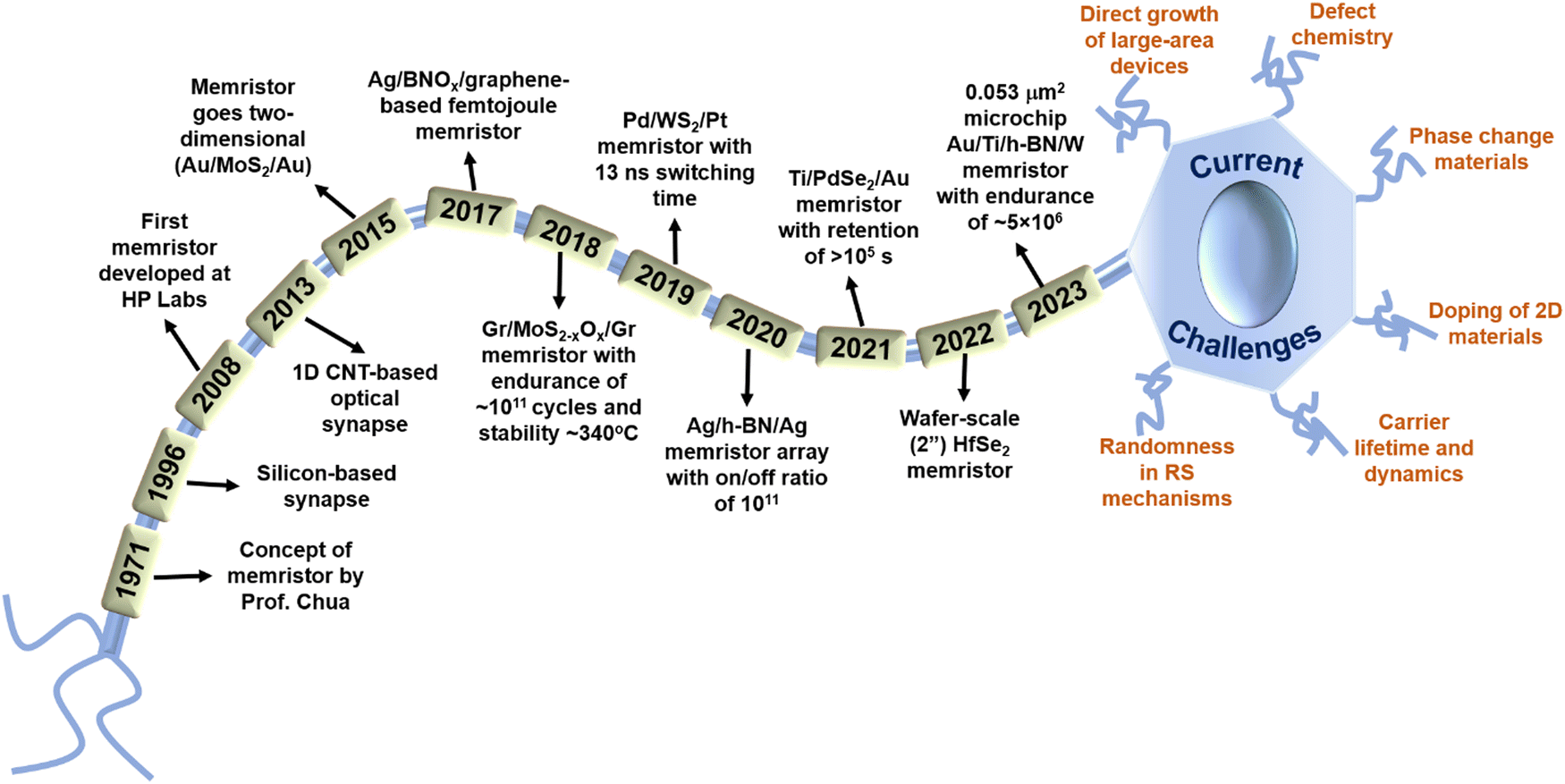 | ||
| Fig. 5 Schematic showing important milestones and the current challenges in the area of brain-inspired computing. | ||
6. Conclusions and outlook
While substantial progress in the area of 2DLM-based artificial synapses has been made in recent years, certain critical issues still need to be addressed for the real-world applications of these emerging devices. Even now, the research on 2DLM-based memristors is in its budding phase, and thus there still remains a large scope for improving these devices.12 Future improvement strategies have been categorized and discussed below:6.1. Regarding growth techniques
• Large area growth and device arrays: present studies on the 2DLM-neuronal devices have mostly focused on single nanodevices, only on the proof-of-concept basis, consisting of layers of 2D materials typically in the range of a few microns.92–97 Few reports have shown large scale growth of 2DLMs to fabricate scalable memristive device arrays,98,99 which is very vital for their commercialization. Currently, most of the reported 2D memristors are fabricated utilizing exfoliation of these 2D materials from their bulk crystals,93 followed by transfer on a substrate. Due to the absence of ultrahigh vacuum, the devices fabricated are often associated with unclean interfaces and thus reduced performance. Therefore, physical vapor deposition techniques such as pulsed laser deposition, molecular beam epitaxy, atomic layer deposition (ALD), etc. should be highly applicable to synthesize ultraclean and atomically thin 2DLM-based memristors.• Cost-effective growth methods: various chemical vapor deposition-based synthesis methods have been successfully reported to fabricate large area 2DLMs; however, drawbacks like high growth temperatures, use of toxic precursors, long processing times, etc.100,101 hinder the use of flexible substrates (mica, paper, polyethylene terephthalate, etc.) for memristor technology.102 Alternative methods such as solution-based techniques (hydrothermal and solvothermal synthesis methods) should be exploited because of their low processing cost and temperature, along with high output.103 However, due to the absence of vacuum during material transfer and device fabrication procedure, utmost care should be taken in order to ensure high device quality, performance, and reliability. Additionally, deposition techniques such as magnetron sputtering and ALD can be utilized for low temperature deposition of 2DLMs.104
6.2. Optimizing defect chemistry and stoichiometry
• Defects: as most of the RS mechanisms depend upon the defects present in the material, engineering and controlling the defect chemistry of a material become very essential for repeatable and reliable memristive devices.18,105 Moreover, Janus structures of TMDCs, referring to transition metal layers having different surfaces, have garnered intensive research interest in recent times in view of their exceptional features that originate because of the symmetry breaking in such structures.106 Hence, these could play a pivotal role in tailoring the memristive characteristics of neuromorphic devices.• Doping: doping of 2DLMs is another key strategy that should be vastly explored for memristive devices, as it would help in precisely controlling the defect states in the material. Additionally, there is an urgent requirement to optimise the p-type doping of 2DLMs, which would facilitate their easy integration with wide band gap n-type semiconductors such as TiO2 or Ga2O3 for realization of p–n diode-based photomemristors.
6.3. Exploiting heterostructures of 2DLMs
• Heterostructures: an alternative approach to design optimum materials is to combine a set of materials with the required properties rather than looking for a single material that possesses all of them. More focus should be put on neuromorphic devices based on heterojunctions of 2DLMs. Utilization of high electron conducting 2D materials such as graphene, graphene derivatives and semi-metallic phases of TMDCs like 1T-MoS2 in place of the traditional metal contacts over 2DLMs may offer new avenues, as these hybrids exhibit excellent electronic properties along with maximizing the area for light absorption, in the case of photomemristors.17,50 Transition metal oxides (TMOs) such as TiO2,14 ZnO,16,107 HfO2,108etc. have been immensely utilized for neuromorphic devices, and thus the oxide technology seems to be somewhat matured in this area. Therefore, integration of 2DLMs with TMOs to form hybrid devices is expected to result in superior performance because these devices can utilize the advantages of both the established technology of TMOs and the unique properties of atomically ultrathin 2D materials.• Band alignment: it is high time to explore heterostructures of 2DLMs with other 2DLMs or traditional semiconductors that show type-III band alignment, such as MoS2/InN,47 SnS2/black phosphorus,109etc., which can be reversibly transformed into type-II, in order to exploit RS based on the mechanism of Schottky barrier and direct tunneling.
• Phase change materials: PCMs exhibiting an exciting phenomenon at the atomic level have always been a topic of interest for many decades and, recently, they have shown a lot of potential in neuromorphic devices.13 Their combination with 2DLMs could be very intriguing in achieving multiple conductance states by exploiting the properties of individual PCMs and the effects of the 2DLM/PCM heterojunction. Moreover, the mechanism of phase transitions in 2DLMs (for instance, the 2H phase to 1T phase in MoS2) should be explored more and more, in order to design energy efficient memristors. These phase transitions, which can be triggered by an external electric field, are associated with a change in the crystal structure too. Repeated transitions in the structure result in mechanical wear and tear, thereby opening new avenues of research on decoupling the change in crystal structure with different conduction states.13
6.4. Stabilizing switching mechanisms
• Suppressing surface oxidation: although 2DLMs have more inert surfaces as compared to the those of non-layered materials, oxidation of exposed surfaces is still thermodynamically favorable for most of the 2DLMs. Consequently, research on the oxidation kinetics of 2DLMs can be an intriguing area of investigation as the unintentional oxide formation might affect the device behavior in both positive and negative ways.• Nanopatterning of substrates: the majority of memristors operate via the growth and dispersion of conducting filaments, and the growth and distribution of these filaments are random.77,110 This affects the reliability and repeatability of such devices, and thus, measures should be taken to minimize randomness in the filament growth. An effective way could be the nano-patterning of the surface using techniques like e-beam lithography or putting seeds on the surface before making the contact electrodes, to facilitate systematic growth of these conducting filaments.
• Mechanisms other than conductive filaments: utilizing resistive switching mechanisms such as changes in the crystal phase and modulation in Schottky barrier height will promote a uniform, reliable and stable switching phenomenon over a large number of endurance cycles.
6.5. Role of nano-structuring
• One-dimensional structures: memory devices based on one-dimensional nanostructures and their heterojunctions are another intriguing field that should be thoroughly explored.107,111 Nanowires and nanorods exhibit several advantages such as charge carrier confinement, high surface to volume ratios, shorter channel lengths, etc.,45 which boost their light harvesting properties. One-dimensional nanorods offer straighter conduction channels that assist in the transport of charge carriers compared to the branched conduction paths, observed in thin films. These direct channels produce outstanding memristive behavior as the resistance states show a narrow distribution in one-dimensional structures.56• Plasmonic and defect passivation: noble metal nanoparticles (NPs) have been utilized in the past due to their fascinating properties such as localized surface plasmon resonance (LSPR),112–114 defect passivation,115etc. Metal NPs such as Au and Pt can be exploited as charge trapping elements in NVS devices due to their large electron affinity, higher chemical stability, easy synthesis procedure, etc. Larger electron affinity extends the charge carrier lifetime, thereby enhancing the memristor's retention characteristics.111 Phenomena like LSPR have been used to modulate photoexcitation of electrons in NP-based composite systems, and defect passivation can be used to tune the defect states in memory devices.
6.6. Theoretical approaches and algorithms, and their integration into existing device assemblies
• Modelling: while the current research on memristors is driven by experiments, computational simulations and modelling using density functional theory (DFT) and molecular dynamics (MD) offer powerful tools to predict charge transfer, electronic band structures, carrier dynamics, etc.,116,117 all of which can be critical for determining the memristor performance. Additionally, simulations also govern stability, defect behavior, and diffusion, expediting material design for better properties. Unraveling intricate atomic-level investigations can accelerate the advancements in high-performance memristors and neuromorphic devices.• Algorithms: current neuromorphic technology may perform exceptionally well in some specialized tasks (such as pattern recognition and sensory processing), but may fall short in more general cognitive activities. It is still difficult to create neuromorphic machines that can perform a variety of cognitive activities. Additionally, the neuromorphic devices try to mimic biological learning and adaptability; however, it is still difficult to develop effective and reliable learning algorithms that can be implemented on hardware. Although there have been convincing examples where neuromorphic solutions outperform other hardware implementations like neural hardware and edge GPUs in terms of energy efficiency, there has not yet been a machine learning algorithm/application combination for which neuromorphic computing significantly outperforms deep learning approaches in terms of accuracy.118 The absence of widely available and usable hardware and software systems for the computer science communities is another major obstacle impeding the development of algorithms and applications for neuromorphic computers. There exist multiple neuromorphic implementations; yet, the quantity of each implementation is constrained, and the broader community can usually obtain them only through restricted cloud access.118
• Issues with integration: last but not least, neuromorphic devices may face competition from more established computing technologies, such as traditional CPUs, GPUs, and AI accelerators. Moreover, the current devices may not be fit to accommodate the neuromorphic chips and parallel computing, and thus, new device assemblies need to be built for the successful integration of these neuromorphic devices. It is probable that a multitude of applications for neuromorphic computers in the future will involve their integration into a more diverse computing environment, as opposed to their standalone usage. Emergent hardware systems, including neuromorphic and quantum computers, will be included in the computing landscape more frequently to speed up specific types of computation due to performance limitations (in terms of energy consumption or processing speed) of current hardware systems.118 Additionally, neuromorphic technology may need to be shown to have definite advantages and value in order to persuade corporations and sectors to invest in and use it.
It is important to note that research and development in the field of neuromorphic computing are ongoing, and recent advancements in neuromorphic devices have shown promising strides towards bridging the gap between biological and AI neural networks. A summary of the progress and future perspectives on 2DLM-based devices for AI is pictorially depicted in Fig. 6. Continuous research and innovation are essential to unlock the full potential of neuromorphic devices and pave the way for a new era of efficient and brain-inspired computing paradigms.
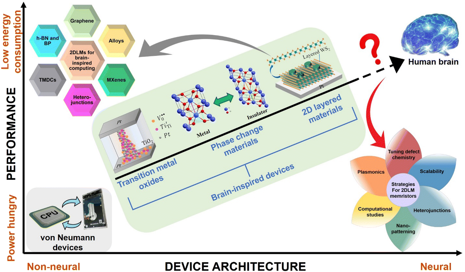 | ||
| Fig. 6 2DLMs for neuromorphic computing. Performance scales up with the advancement of the design architecture, ranging from von Neumann devices to neuromorphic systems. The ultimate target is to design devices mimicking brain's activity and matching its efficiency. Recent progress in memristors fabricated utilizing TMOs, PCMs, and 2DLMs, and with certain strategic modifications in different 2DLMs, devices emulating intelligence and critical for non-von Neumann machines can be designed. Reproduced with permission from ref. 87, 119 and 120. Copyright 2019, John Wiley & Sons, Inc.; copyright 2023, Springer Nature; copyright 2020, Frontiers. | ||
Conflicts of interest
The authors have no conflicts to disclose.Acknowledgements
The authors would like to convey their gratitude to the Director, CSIR-NPL, New Delhi, India for his constant support. D. K. S. is grateful to Dr. Madhubanti Mukherjee, Georgia Institute of Technology, United States of America for providing help with making figures. The digital photo of the human brain (Fig. 1) and the schematic of neurons (Fig. 2) have been adapted from images designed using iuriimotov/Freepik and macrovector/Freepik, respectively. D. K. S. is thankful to the DST-INSPIRE Faculty Fellowship (Faculty Registration No.: IFA22-MS 187) for providing financial support.References
- M. Mukherjee, S. Satsangi and A. K. Singh, A Statistical Approach for the Rapid Prediction of Electron Relaxation Time Using Elemental Representatives, Chem. Mater., 2020, 32(15), 6507–6514 CrossRef CAS.
- A. Jain, S. P. Ong, G. Hautier, W. Chen, W. D. Richards, S. Dacek, S. Cholia, D. Gunter, D. Skinner, G. Ceder and K. A. Persson, Commentary: The Materials Project: A Materials Genome Approach to Accelerating Materials Innovation, APL Mater., 2013, 1(1), 011002 CrossRef.
- H. H. Radamson, H. Zhu, Z. Wu, X. He, H. Lin, J. Liu, J. Xiang, Z. Kong, W. Xiong, J. Li, H. Cui, J. Gao, H. Yang, Y. Du, B. Xu, B. Li, X. Zhao, J. Yu, Y. Dong and G. Wang, State of the Art and Future Perspectives in Advanced CMOS Technology, Nanomaterials, 2020, 10(8), 1555 CrossRef CAS PubMed.
- A. Razavieh, P. Zeitzoff and E. J. Nowak, Challenges and Limitations of CMOS Scaling for FinFET and Beyond Architectures, IEEE Trans. Nanotechnol., 2019, 18, 999–1004 CAS.
- R. K. Maurya and B. Bhowmick, Review of FinFET Devices and Perspective on Circuit Design Challenges, Silicon, 2022, 14(11), 5783–5791 CrossRef CAS.
- K. Benaissa, Y. Jau-Yuann, D. Crenshaw, B. Williams, S. Sridhar, A. Johnny, G. Boselli, Z. Song, T. Shaoping, S. Ashburn, P. Madhani, T. Blythe, N. Mahalingam and H. Shichijo, RF CMOS on High-Resistivity Substrates for System-on-Chip Applications, IEEE Trans. Electron Devices, 2003, 50(3), 567–576 CrossRef.
- E. Chanrion, D. J. Niegemann, B. Bertrand, C. Spence, B. Jadot, J. Li, P.-A. Mortemousque, L. Hutin, R. Maurand, X. Jehl, M. Sanquer, S. De Franceschi, C. Bäuerle, F. Balestro, Y.-M. Niquet, M. Vinet, T. Meunier and M. Urdampilleta, Charge Detection in an Array of CMOS Quantum Dots, Phys. Rev. Appl., 2020, 14(2), 024066 CrossRef CAS.
- H. J. Yun, J. Lim, J. Roh, D. C. J. Neo, M. Law and V. I. Klimov, Solution-Processable Integrated CMOS Circuits Based on Colloidal CuInSe2 Quantum Dots, Nat. Commun., 2020, 11(1), 5280 CrossRef CAS PubMed.
- A. C. Betz, M. L. V. Tagliaferri, M. Vinet, M. Broström, M. Sanquer, A. J. Ferguson and M. F. Gonzalez-Zalba, Reconfigurable Quadruple Quantum Dots in a Silicon Nanowire Transistor, Appl. Phys. Lett., 2016, 108(20), 203108 CrossRef.
- L. Wang, X. Shen, Z. Gao, J. Fu, S. Yao, L. Cheng and X. Lian, Review of Applications of 2D Materials in Memristive Neuromorphic Circuits, J. Mater. Sci., 2022, 57(8), 4915–4940 CrossRef CAS.
- V. A. Bespalov and N. A. Dyuzhev, Kireev, V. Yu. Possibilities and Limitations of CMOS Technology for the Production of Various Microelectronic Systems and Devices, Nanotechnol. Russia, 2022, 17(1), 24–38 CrossRef.
- W. Huh, D. Lee and C. Lee, Memristors Based on 2D Materials as an Artificial Synapse for Neuromorphic Electronics, Adv. Mater., 2020, 32(51), 2002092 CrossRef CAS PubMed.
- H.-T. Zhang, P. Panda, J. Lin, Y. Kalcheim, K. Wang, J. W. Freeland, D. D. Fong, S. Priya, I. K. Schuller, S. K. R. S. Sankaranarayanan, K. Roy and S. Ramanathan, Organismic Materials for beyond von Neumann Machines, Appl. Phys. Rev., 2020, 7(1), 011309 CAS.
- M. C. Sahu, A. K. Jena, S. K. Mallik, S. Roy, S. Sahoo, R. S. Ajimsha, P. Misra and S. Sahoo, Reconfigurable Low-Power TiO2 Memristor for Integration of Artificial Synapse and Nociceptor, ACS Appl. Mater. Interfaces, 2023, 15(21), 25713–25725 CrossRef CAS PubMed.
- M. Asif, Y. Singh, A. Thakre, V. N. Singh and A. Kumar, Synaptic Plasticity and Learning Behaviour in Multilevel Memristive Devices, RSC Adv., 2023, 13(19), 13292–13302 RSC.
- R. Mandal, A. Mandal, A. Mitra and T. Som, Emulation of Bio-Synaptic Behaviours in Copper-Doped Zinc Oxide Memristors: A Nanoscale Scanning Probe Microscopic Study, Appl. Surf. Sci., 2022, 606, 154860 CrossRef CAS.
- P. Cheng, K. Sun and Y. H. Hu, Memristive Behavior and Ideal Memristor of 1T Phase MoS2 Nanosheets, Nano Lett., 2016, 16(1), 572–576 CrossRef CAS PubMed.
- K. Rudrapal, M. Biswas, B. Jana, V. Adyam and A. R. Chaudhuri, Tuning resistive switching properties of WO3−x-memristors by oxygen vacancy engineering for neuromorphic and memory storage applications, J. Phys. D: Appl. Phys., 2023, 56(20), 205302 CrossRef.
- L. Chua, Memristor-The Missing Circuit Element, IEEE Trans. Circuit Theory, 1971, 18(5), 507–519 Search PubMed.
- C. Mead, Neuromorphic Electronic Systems, Proc. IEEE, 1990, 78(10), 1629–1636 CrossRef.
- G. Indiveri, B. Linares-Barranco, T. J. Hamilton, A. V. Schaik, R. Etienne-Cummings, T. Delbruck, S.-C. Liu, P. Dudek, P. Häfliger, S. Renaud, J. Schemmel, G. Cauwenberghs, J. Arthur, K. Hynna, F. Folowosele, S. Saighi, T. Serrano-Gotarredona, J. Wijekoon, Y. Wang and K. Boahen, Neuromorphic Silicon Neuron Circuits, Front. Neurosci., 2011, 5, 73 Search PubMed.
- W. Zhang, B. Gao, J. Tang, P. Yao, S. Yu, M.-F. Chang, H.-J. Yoo, H. Qian and H. Wu, Neuro-Inspired Computing Chips, Nat. Electron, 2020, 3(7), 371–382 CrossRef.
- W. Wan, R. Kubendran, C. Schaefer, S. B. Eryilmaz, W. Zhang, D. Wu, S. Deiss, P. Raina, H. Qian, B. Gao, S. Joshi, H. Wu, H.-S. P. Wong and G. Cauwenberghs, A Compute-in-Memory Chip Based on Resistive Random-Access Memory, Nature, 2022, 608(7923), 504–512 CrossRef CAS PubMed.
- S. Ambrogio, P. Narayanan, H. Tsai, R. M. Shelby, I. Boybat, C. Di Nolfo, S. Sidler, M. Giordano, M. Bodini, N. C. P. Farinha, B. Killeen, C. Cheng, Y. Jaoudi and G. W. Burr, Equivalent-Accuracy Accelerated Neural-Network Training Using Analogue Memory, Nature, 2018, 558(7708), 60–67 CrossRef CAS PubMed.
- M. Lavzin, S. Rapoport, A. Polsky, L. Garion and J. Schiller, Nonlinear Dendritic Processing Determines Angular Tuning of Barrel Cortex Neurons in Vivo, Nature, 2012, 490(7420), 397–401 CrossRef CAS PubMed.
- P. Yao, H. Wu, B. Gao, J. Tang, Q. Zhang, W. Zhang, J. J. Yang and H. Qian, Fully Hardware-Implemented Memristor Convolutional Neural Network, Nature, 2020, 577(7792), 641–646 CrossRef CAS PubMed.
- J. Zhang, Z. Wang and N. Verma, In-Memory Computation of a Machine-Learning Classifier in a Standard 6T SRAM Array, IEEE J. Solid-State Circuits, 2017, 52(4), 915–924 Search PubMed.
- C. Frenkel, M. Lefebvre, J.-D. Legat and D. Bol, A 0.086 mm2 12.7 pJ/SOP 64k-Synapse 256-Neuron Online-Learning Digital Spiking Neuromorphic Processor in 28 nm CMOS, IEEE Trans. Biomed. Circuits Syst, 2018, 13(1), 145 Search PubMed.
- S. B. Furber, F. Galluppi, S. Temple and L. A. Plana, The SpiNNaker Project, Proc. IEEE, 2014, 102(5), 652–665 Search PubMed.
- V. K. Sangwan and M. C. Hersam, Neuromorphic Nanoelectronic Materials, Nat. Nanotechnol., 2020, 15(7), 517–528 CrossRef CAS PubMed.
- F. Akopyan, J. Sawada, A. Cassidy, R. Alvarez-Icaza, J. Arthur, P. Merolla, N. Imam, Y. Nakamura, P. Datta, G.-J. Nam, B. Taba, M. Beakes, B. Brezzo, J. B. Kuang, R. Manohar, W. P. Risk, B. Jackson and D. S. Modha, TrueNorth: Design and Tool Flow of a 65 mW 1 Million Neuron Programmable Neurosynaptic Chip, IEEE Trans. Comput.-Aided Des. Integr. Circuits Syst, 2015, 34(10), 1537–1557 Search PubMed.
- M. Davies, N. Srinivasa, T.-H. Lin, G. Chinya, Y. Cao, S. H. Choday, G. Dimou, P. Joshi, N. Imam, S. Jain, Y. Liao, C.-K. Lin, A. Lines, R. Liu, D. Mathaikutty, S. McCoy, A. Paul, J. Tse, G. Venkataramanan, Y.-H. Weng, A. Wild, Y. Yang and H. Wang, Loihi: A Neuromorphic Manycore Processor with On-Chip Learning, IEEE Micro, 2018, 38(1), 82–99 Search PubMed.
- M. K. Thakur, A. Gupta, M. Y. Fakhri, R. S. Chen, C. T. Wu, K. H. Lin and S. Chattopadhyay, Optically Coupled Engineered Upconversion Nanoparticles and Graphene for a High Responsivity Broadband Photodetector, Nanoscale, 2019, 11(19), 9716–9725 RSC.
- A. Sharma, U. Varshney, P. Vashishtha, A. Yadav, P. Prajapat, P. Singh and G. Gupta, Self-Driven Vis-NIR Broadband Photodetector Based on Nano-Hedge-like MoS2/WSe2 Heterostructure, Mater. Sci. Semicond. Process., 2023, 164, 107611 CrossRef CAS.
- T. Kim, T. H. Lee, S. Y. Park, T. H. Eom, I. Cho, Y. Kim, C. Kim, S. A. Lee, M. J. Choi, J. M. Suh and I. S. Hwang, Drastic Gas Sensing Selectivity in 2-Dimensional MoS2 Nanoflakes by Noble Metal Decoration, ACS Nano, 2023, 17(5), 4404–4413 CrossRef CAS PubMed.
- P. Vashishtha, P. Prajapat, A. Sharma, P. Goswami, S. Walia and G. Gupta, Self-Driven and Thermally Resilient Highly Responsive Nano-Fenced MoS2 Based Photodetector for near-Infrared Optical Signal, Mater. Res. Bull., 2023, 164, 112260 CrossRef CAS.
- S. Yang, M. Choi and C. Kim, Engineering Grain Boundaries in Two-Dimensional Electronic Materials, Adv. Mater., 2023, 35(4), 2203425 CrossRef CAS PubMed.
- P. Kumbhakar, M. Mukherjee, A. Pramanik, S. Karmakar, A. K. Singh, C. S. Tiwary and P. Kumbhakar, Confinement Aided Simultanous Water Cleaning and Energy Harvesting Using Atomically Thin Wurtzite (Wurtzene), Adv. Sustainable Systems, 2021, 5(2), 2000189 CrossRef CAS.
- U. Varshney, A. Sharma, P. Vashishtha, P. Singh and G. Gupta, Highly responsive self-driven broadband photodetector based on MoS2 nanorods/β-Ga2O3 heterojunction, Mater. Sci. Semicond. Process., 2023, 164, 107612 CrossRef CAS.
- D. K. Singh, R. K. Pant, K. K. Nanda and S. B. Krupanidhi, Differentiation of Ultraviolet/Visible Photons from near Infrared Photons by MoS2/GaN/Si-Based Photodetector, Appl. Phys. Lett., 2021, 119(12), 121102 CrossRef CAS.
- P. Kumbhakar, C. Chowde Gowda, P. L. Mahapatra, M. Mukherjee, K. D. Malviya, M. Chaker, A. Chandra, B. Lahiri, P. M. Ajayan, D. Jariwala, A. Singh and C. S. Tiwary, Emerging 2D Metal Oxides and Their Applications, Mater. Today, 2021, 45, 142–168 CrossRef CAS.
- P. Prajapat, P. Vashishtha, P. Goswami and G. Gupta, Fabrication of Sb2Se3-Based High-Performance Self-Powered Visible-NIR Broadband Photodetector, Mater. Sci. Semicond. Process., 2024, 169, 107873 CrossRef CAS.
- D. K. Singh, R. Pant, A. M. Chowdhury, B. Roul, K. K. Nanda and S. B. Krupanidhi, Defect-Mediated Transport in Self-Powered, Broadband, and Ultrafast Photoresponse of a MoS2/AlN/Si-Based Photodetector, ACS Appl. Electron. Mater., 2020, 2(4), 944–953 CrossRef CAS.
- P. Goswami, P. Vashishtha, A. Yadav, P. Prajapat, L. Goswami and G. Gupta, Fabrication of Highly Sensitive Visible Photodetector Based on SnS2 Terrazzo-like Structure for Weak Signal Detection, Opt. Mater., 2023, 145, 114406 CrossRef CAS.
- D. K. Singh, R. K. Pant, K. K. Nanda and S. B. Krupanidhi, Pulsed Laser Deposition for Conformal Growth of MoS2 on GaN Nanorods for Highly Efficient Self-Powered Photodetection, Mater. Adv, 2022, 3(15), 6343–6351 RSC.
- H. Tang, B. Neupane, S. Neupane, S. Ruan, N. K. Nepal and A. Ruzsinszky, Tunable Band Gaps and Optical Absorption Properties of Bent MoS2 Nanoribbons, Sci. Rep., 2022, 12(1), 3008 CrossRef CAS PubMed.
- D. K. Singh, B. Roul, R. Pant, A. M. Chowdhury, K. K. Nanda and S. B. Krupanidhi, Different Types of Band Alignment at MoS2/(Al, Ga, In)N Heterointerfaces, Appl. Phys. Lett., 2020, 116(25), 252102 CrossRef CAS.
- L. Wang, W. Chen, D. Zhang, Y. Du, R. Amal, S. Qiao, J. Wu and Z. Yin, Surface Strategies for Catalytic CO2 Reduction: From Two-Dimensional Materials to Nanoclusters to Single Atoms, Chem. Soc. Rev., 2019, 48(21), 5310–5349 RSC.
- H. Duan, S. Cheng, L. Qin, X. Zhang, B. Xie, Y. Zhang and W. Jie, Low-Power Memristor Based on Two-Dimensional Materials, J. Phys. Chem. Lett., 2022, 13(31), 7130–7138 CrossRef CAS PubMed.
- K. Zhou, Z. Jia, X.-Q. Ma, W. Niu, Y. Zhou, N. Huang, G. Ding, Y. Yan, S.-T. Han, V. A. L. Roy and Y. Zhou, Manufacturing of Graphene Based Synaptic Devices for Optoelectronic Applications, Int. J. Extrem. Manuf., 2023, 5(4), 042006 CrossRef.
- A. T. Buruiana, A. E. Bocirnea, A. C. Kuncser, T. Tite, E. Matei, C. Mihai, N. Zawadzka, K. Olkowska-Pucko, Ł. Kipczak, A. Babiński, M. R. Molas, A. Velea and A. C. Galca, Layered SnSe Nanoflakes with Anharmonic Phonon Properties and Memristive Characteristics, Appl. Surf. Sci., 2022, 599, 153983 CrossRef CAS.
- W. Wang, G. N. Panin, X. Fu, L. Zhang, P. Ilanchezhiyan, V. O. Pelenovich, D. Fu and T. W. Kang, MoS2 Memristor with Photoresistive Switching, Sci. Rep., 2016, 6(1), 31224 CrossRef CAS PubMed.
- S. Saha, V. Adepu, K. Gohel, P. Sahatiya and S. S. Dan, Demonstration of a 2-D SnS/MXene Nanohybrid Asymmetric Memristor, IEEE Trans. Electron Devices, 2022, 69(10), 5921–5927 CAS.
- K. Tang, Y. Wang, C. Gong, C. Yin, M. Zhang, X. Wang and J. Xiong, Electronic and Photoelectronic Memristors Based on 2D Materials, Adv. Electron. Mater., 2022, 8(4), 2101099 CrossRef CAS.
- C. Wang, C. Wang, F. Meng, P. Wang, S. Wang, S. Liang and F. Miao, 2D Layered Materials for Memristive and Neuromorphic Applications, Adv. Electron. Mater., 2020, 6(2), 1901107 CrossRef CAS.
- C.-C. Chiang, V. Ostwal, P. Wu, C.-S. Pang, F. Zhang, Z. Chen and J. Appenzeller, Memory Applications from 2D Materials, Appl. Phys. Rev., 2021, 8(2), 021306 CAS.
- J. Lin, S. Guha and S. Ramanathan, Vanadium Dioxide Circuits Emulate Neurological Disorders, Front. Neurosci., 2018, 12, 856 CrossRef PubMed.
- J. Mao, L. Zhou, X. Zhu, Y. Zhou and S. Han, Photonic Memristor for Future Computing: A Perspective, Adv. Opt. Mater., 2019, 7(22), 1900766 CrossRef CAS.
- S. Batool, M. Idrees, S.-R. Zhang, S.-T. Han and Y. Zhou, Novel Charm of 2D Materials Engineering in Memristor: When Electronics Encounter Layered Morphology, Nanoscale Horiz., 2022, 7(5), 480–507 RSC.
- A. K. Jena, M. C. Sahu, K. U. Mohanan, S. K. Mallik, S. Sahoo, G. K. Pradhan and S. Sahoo, Bipolar Resistive Switching in TiO2 Artificial Synapse Mimicking Pavlov's Associative Learning, ACS Appl. Mater. Interfaces, 2023, 15(2), 3574–3585 CrossRef CAS PubMed.
- P. Prajapat, P. Vashishtha, P. Goswami and G. Gupta, Fabrication of Sb2S3/Sb2Se3 Heterostructure for Potential Resistive Switching Applications, Nano Ex., 2024, 5(1), 015005 CrossRef.
- K. Yang, Y. Huan, J. Xu, Z. Zou, Y. Zhan, L. Zheng and F. Seoane, Universal and Convenient Optimization Strategies for Three-Terminal Memristors, IEEE Access, 2018, 6, 48815–48826 Search PubMed.
- D. B. Strukov, G. S. Snider, D. R. Stewart and R. S. Williams, The Missing Memristor Found, Nature, 2008, 453(7191), 80–83 CrossRef CAS PubMed.
- S. A. Chekol, S. Menzel, R. W. Ahmad, R. Waser and S. Hoffmann-Eifert, Effect of the Threshold Kinetics on the Filament Relaxation Behavior of Ag-Based Diffusive Memristors, Adv. Funct. Mater., 2022, 32(15), 2111242 CrossRef CAS.
- A. Chanthbouala, V. Garcia, R. O. Cherifi, K. Bouzehouane, S. Fusil, X. Moya, S. Xavier, H. Yamada, C. Deranlot, N. D. Mathur, M. Bibes, A. Barthélémy and J. Grollier, A Ferroelectric Memristor, Nat. Mater., 2012, 11(10), 860–864 CrossRef CAS PubMed.
- H. Sun, Z. Luo, L. Zhao, C. Liu, C. Ma, Y. Lin, G. Gao, Z. Chen, Z. Bao, X. Jin and Y. Yin, BiFeO3-based flexible ferroelectric memristors for neuromorphic pattern recognition, ACS Appl. Electron. Mater., 2020, 2(4), 1081–1089 CrossRef CAS.
- R. Sbiaa and S. N. Piramanayagam, Recent Developments in Spin Transfer Torque MRAM, Phys. Status. Solidi Rapid Res. Lett., 2017, 11(12), 1700163 CrossRef.
- W. Xiaobin and Y. Chen. Spintronic Memristor Devices and Application, 2010 Design, Automation & Test in Europe Conference & Exhibition (DATE 2010), IEEE, Dresden, 2010, pp. 667–672 Search PubMed.
- M. K. Park, H. N. Yoo, Y. T. Seo, S. Y. Woo, J. H. Bae, B. G. Park and J. H. Lee, Field effect transistor-type devices using high-κ gate insulator stacks for neuromorphic applications, ACS Appl. Electron. Mater., 2019, 2(2), 323–328 CrossRef.
- S. Choi, S. Kim, J. Jang, G. Ahn, J. T. Jang, J. Yoon, T. J. Park, B.-G. Park, D. M. Kim, S.-J. Choi, S. M. Lee, E. Y. Kim, H. S. Mo and D. H. Kim, Implementing an Artificial Synapse and Neuron Using a Si Nanowire Ion-Sensitive Field-Effect Transistor and Indium-Gallium-Zinc-Oxide Memristors, Sens. Actuators, B, 2019, 296, 126616 CrossRef CAS.
- V. K. Sangwan, D. Jariwala, I. S. Kim, K.-S. Chen, T. J. Marks, L. J. Lauhon and M. C. Hersam, Gate-Tunable Memristive Phenomena Mediated by Grain Boundaries in Single-Layer MoS2, Nat. Nanotechnol., 2015, 10(5), 403–406 CrossRef CAS PubMed.
- A. Mansingh, R. Singh and S. B. Krupanidhi, Electrical Switching in Single Crystal VO2, Solid-State Electron., 1980, 23(6), 649–654 CrossRef CAS.
- D. Bhardwaj, D. K. Singh, S. B. Krupanidhi and A. M. Umarji, Fabrication of Smooth Thin Film of Vanadium Oxides (VOx) Using Pulsed Laser Deposition, Appl. Phys. A: Mater. Sci. Process., 2020, 126(3), 157 CrossRef CAS.
- A. Mansingh, R. Singh and M. Sayer, Low frequency dielectric relaxation in lightly doped VO2 single crystals, J. Phys. Chem. Solids, 1984, 45(1), 79–88 CrossRef CAS.
- K. Chang, X. Hai, H. Pang, H. Zhang, L. Shi, G. Liu, H. Liu, G. Zhao, M. Li and J. Ye, Targeted Synthesis of 2H- and 1T-Phase MoS2 Monolayers for Catalytic Hydrogen Evolution, Adv. Mater., 2016, 28(45), 10033–10041 CrossRef CAS PubMed.
- K. L. Okabe, A. Sood, E. Yalon, C. M. Neumann, M. Asheghi, E. Pop, K. E. Goodson and H.-S. P. Wong, Understanding the Switching Mechanism of Interfacial Phase Change Memory, J. Appl. Phys., 2019, 125(18), 184501 CrossRef.
- Z. Zhou, J. Zhao, A. P. Chen, Y. Pei, Z. Xiao, G. Wang, J. Chen, G. Fu and X. Yan, Designing Carbon Conductive Filament Memristor Devices for Memory and Electronic Synapse Applications, Mater. Horiz., 2020, 7(4), 1106–1114 RSC.
- R. Wang, J.-Q. Yang, J.-Y. Mao, Z.-P. Wang, S. Wu, M. Zhou, T. Chen, Y. Zhou and S.-T. Han, Recent Advances of Volatile Memristors: Devices, Mechanisms, and Applications, Adv. Intell. Syst., 2020, 2(9), 2000055 CrossRef.
- S. Yin, Z. Luo, Q. Li, C. Xiong, Y. Liu, R. Singh, F. Zeng, Y. Zhong and X. Zhang, Emulation of Learning and Memory Behaviors by Memristor Based on Ag Migration on 2D MoS2 Surface, Phys. Status Solidi A, 2019, 216(14), 1900104 CrossRef.
- Y. Tian, L. Jiang, X. Zhang, G. Zhang and Q. Zhu, Trap-Assisted Transition between Schottky Emission and Fowler-Nordheim Tunneling in the Interfacial-Memristor Based on Bi2S3 Nano-Networks, AIP Adv., 2018, 8(3), 035105 CrossRef.
- T. Zhang, M. Yin, C. Xu, X. Lu, X. Sun, Y. Yang and R. Huang, High-Speed True Random Number Generation Based on Paired Memristors for Security Electronics, Nanotechnology, 2017, 28(45), 455202 CrossRef PubMed.
- H. Chen, Y. Kang, D. Pu, M. Tian, N. Wan, Y. Xu, B. Yu, W. Jie and Y. Zhao, Introduction of Defects in Hexagonal Boron Nitride for Vacancy-Based 2D Memristors, Nanoscale, 2023, 15(9), 4309–4316 RSC.
- R. Ge, X. Wu, M. Kim, J. Shi, S. Sonde, L. Tao, Y. Zhang, J. C. Lee and D. Akinwande, Atomristor: Nonvolatile Resistance Switching in Atomic Sheets of Transition Metal Dichalcogenides, Nano Lett., 2018, 18(1), 434–441 CrossRef CAS PubMed.
- K. Gacem, J.-M. Retrouvey, D. Chabi, A. Filoramo, W. Zhao, J.-O. Klein and V. Derycke, Neuromorphic Function Learning with Carbon Nanotube Based Synapses, Nanotechnology, 2013, 24(38), 384013 CrossRef PubMed.
- H. Zhao, Z. Dong, H. Tian, D. DiMarzi, M. Han, L. Zhang, X. Yan, F. Liu, L. Shen, S. Han, S. Cronin, W. Wu, J. Tice, J. Guo and H. Wang, Atomically Thin Femtojoule Memristive Device, Adv. Mater., 2017, 29(47), 1703232 CrossRef PubMed.
- M. Wang, S. Cai, C. Pan, C. Wang, X. Lian, Y. Zhuo, K. Xu, T. Cao, X. Pan, B. Wang, S.-J. Liang, J. J. Yang, P. Wang and F. Miao, Robust Memristors Based on Layered Two-Dimensional Materials, Nat. Electron, 2018, 1(2), 130–136 CrossRef CAS.
- X. Yan, Q. Zhao, A. P. Chen, J. Zhao, Z. Zhou, J. Wang, H. Wang, L. Zhang, X. Li, Z. Xiao, K. Wang, C. Qin, G. Wang, Y. Pei, H. Li, D. Ren, J. Chen and Q. Liu, Vacancy-Induced Synaptic Behavior in 2D WS2 Nanosheet–Based Memristor for Low-Power Neuromorphic Computing, Small, 2019, 15(24), 1901423 CrossRef PubMed.
- S. Chen, M. R. Mahmoodi, Y. Shi, C. Mahata, B. Yuan, X. Liang, C. Wen, F. Hui, D. Akinwande, D. B. Strukov and M. Lanza, Wafer-Scale Integration of Two-Dimensional Materials in High-Density Memristive Crossbar Arrays for Artificial Neural Networks, Nat. Electron, 2020, 3(10), 638–645 CrossRef CAS.
- Y. Li, L. Loh, S. Li, L. Chen, B. Li, M. Bosman and K.-W. Ang, Anomalous Resistive Switching in Memristors Based on Two-Dimensional Palladium Diselenide Using Heterophase Grain Boundaries, Nat. Electron, 2021, 4(5), 348–356 CrossRef CAS.
- S. Li, M. Pam, Y. Li, L. Chen, Y. Chien, X. Fong, D. Chi and K. Ang, Wafer-Scale 2D Hafnium Diselenide Based Memristor Crossbar Array for Energy-Efficient Neural Network Hardware, Adv. Mater., 2022, 34(25), 2103376 CrossRef CAS PubMed.
- K. Zhu, S. Pazos, F. Aguirre, Y. Shen, Y. Yuan, W. Zheng, O. Alharbi, M. A. Villena, B. Fang, X. Li, A. Milozzi, M. Farronato, M. Muñoz-Rojo, T. Wang, R. Li, H. Fariborzi, J. B. Roldan, G. Benstetter, X. Zhang, H. N. Alshareef, T. Grasser, H. Wu, D. Ielmini and M. Lanza, Hybrid 2D-CMOS Microchips for Memristive Applications, Nature, 2023, 618, 57–62 CrossRef CAS PubMed.
- S. Luo, K. Liao, P. Lei, T. Jiang, S. Chen, Q. Xie, W. Luo, W. Huang, S. Yuan, W. Jie and J. Hao, A Synaptic Memristor Based on Two-Dimensional Layered WSe2 Nanosheets with Short- and Long-Term Plasticity, Nanoscale, 2021, 13(13), 6654–6660 RSC.
- X. Xiong, F. Wu, Y. Ouyang, Y. Liu, Z. Wang, H. Tian and M. Dong, Oxygen Incorporated MoS2 for Rectification-Mediated Resistive Switching and Artificial Neural Network, Adv. Funct. Mater., 2023, 2213348, DOI:10.1002/adfm.202213348.
- F. Huang, C. Ke, J. Li, L. Chen, J. Yin, X. Li, Z. Wu, C. Zhang, F. Xu, Y. Wu and J. Kang, Controllable Resistive Switching in ReS2/WS2 Heterostructure for Nonvolatile Memory and Synaptic Simulation, Adv. Sci., 2023, 10(28), 2302813 CrossRef CAS PubMed.
- Y.-W. Song, M.-K. Song, D. Choi and J.-Y. Kwon, Encapsulation-Enhanced Switching Stability of MoS2 Memristors, J. Alloys Compd., 2021, 885, 161016 CrossRef CAS.
- D. Li, B. Ryu, J. Yoon, Z. Li and X. Liang, Improvement of Analogue Switching Characteristics of MoS2 Memristors through Plasma Treatment, J. Phys. D: Appl. Phys., 2020, 53(13), 135305 CrossRef CAS.
- P. Liu, H. Luo, X. Yin, X. Wang, X. He, J. Zhu, H. Xue, W. Mao and Y. Pu, A Memristor Based on Two-Dimensional MoSe2/MoS2 Heterojunction for Synaptic Device Application, Appl. Phys. Lett., 2022, 121(23), 233501 CrossRef CAS.
- M. Naqi, M. S. Kang, N. Liu, T. Kim, S. Baek, A. Bala, C. Moon, J. Park and S. Kim, Multilevel Artificial Electronic Synaptic Device of Direct Grown Robust MoS2 Based Memristor Array for In-Memory Deep Neural Network, npj 2D Mater. Appl., 2022, 6(1), 53 CrossRef CAS.
- A. Dodda, D. Jayachandran, S. Subbulakshmi Radhakrishnan, A. Pannone, Y. Zhang, N. Trainor, J. M. Redwing and S. Das, Bioinspired and Low-Power 2D Machine Vision with Adaptive Machine Learning and Forgetting, ACS Nano, 2022, 16(12), 20010–20020 CrossRef CAS PubMed.
- J.-S. Rhyee, J. Kwon, P. Dak, J. H. Kim, S. M. Kim, J. Park, Y. K. Hong, W. G. Song, I. Omkaram, M. A. Alam and S. Kim, High-Mobility Transistors Based on Large-Area and Highly Crystalline CVD-Grown MoSe2 Films on Insulating Substrates, Adv. Mater., 2016, 28(12), 2316–2321 CrossRef CAS PubMed.
- D. K. Singh, R. Pant, B. Roul, A. M. Chowdhury, K. K. Nanda and S. B. Krupanidhi, Temperature-Dependent Electrical Transport and Optoelectronic Properties of SnS2/p-Si Heterojunction, ACS Appl. Electron. Mater., 2020, 2(7), 2155–2163 CrossRef CAS.
- J. Chen, J. Xu, L. Gao, C. Yang, T. Guo, J. Chen, Y. Zhao, Y. Xiao, J. Wang and Y. Li, Robust Lateral Structure Memristor Based on MoS2 Synthesized by CVD, J. Electron. Mater., 2022, 51(10), 5832–5841 CrossRef CAS.
- V. Dhyani, P. Kumari, S. Maity and S. Das, Low cost flexible 1.1–1.6 μm photodetector fabricated by hydrothermal grown large area MoSe2 nanostructures, Proc. SPIE Opt. Sensors, 2019, 11028, 110282G, DOI:10.1117/12.2521949.
- T.-J. Dai, X.-D. Fan, Y.-X. Ren, S. Hou, Y.-Y. Zhang, L.-X. Qian, Y.-R. Li and X.-Z. Liu, Layer-Controlled Synthesis of Wafer-Scale MoSe2 Nanosheets for Photodetector Arrays, J. Mater. Sci., 2018, 53(11), 8436–8444 CrossRef CAS.
- G. Moon, S. Y. Min, C. Han, S. Lee, H. Ahn, S. Seo, F. Ding, S. Kim and M. Jo, Atomically Thin Synapse Networks on van der Waals Photo-Memtransistors, Adv. Mater., 2023, 35(4), 2203481 CrossRef CAS PubMed.
- J. Xu, K. Leng, X. Huang, Y. Ye and J. Gong, Artificial Synapses Based on Electric Stress Induced Conductance Variation in Vertical MoReS3 Nanosheets, Appl. Phys. Lett., 2021, 119(26), 263101 CrossRef CAS.
- J. Park, S. Lee, J. Lee and K. Yong, A Light Incident Angle Switchable ZnO Nanorod Memristor: Reversible Switching Behavior Between Two Non-Volatile Memory Devices, Adv. Mater., 2013, 25(44), 6423–6429 CrossRef CAS PubMed.
- Z. Peng, F. Wu, L. Jiang, G. Cao, B. Jiang, G. Cheng, S. Ke, K. Chang, L. Li and C. Ye, HfO2-Based Memristor as an Artificial Synapse for Neuromorphic Computing with Tri-Layer HfO2/BiFeO3/HfO2 Design, Adv. Funct. Mater., 2021, 31(48), 2107131 CrossRef CAS.
- T. Lei, W. Lv, W. Lv, L. Zhang, B. Cui, H. Tu, X. Zhang and W. Shi, Zeng, Z. High Detectivity and Responsivity in Black Phosphorus/SnS2 Heterostructure with Broken-Gap Energy Band Alignment, Jpn. J. Appl. Phys., 2021, 60(6), 065003 CrossRef CAS.
- H.-L. Park, M.-H. Kim and S.-H. Lee, Control of Conductive Filament Growth in Flexible Organic Memristor by Polymer Alignment, Org. Electron., 2020, 87, 105927 CrossRef CAS.
- K. K. Kashyap, L. H. J. Jire and P. Chinnamuthu, A Perspective Study on Au-Nanoparticle Adorned TiO2-Nanowire for Non-Volatile Memory Devices, Mater. Today Commun., 2022, 33, 104469 CrossRef CAS.
- J. Saroha, N. P. Lalla, M. Kumar and S. N. Sharma, Ultrafast Transient Absorption Spectroscopic Studies on the Impact of Growth Time on Size, Stability, and Optical Characteristics of Colloidal Gold Nanoparticles, Optik, 2022, 268, 169759 CrossRef CAS.
- S. Liu, A. S. Arce, S. Nilsson, D. Albinsson, L. Hellberg, S. Alekseeva and C. Langhammer, In Situ Plasmonic Nanospectroscopy of the CO Oxidation Reaction over Single Pt Nanoparticles, ACS Nano, 2019, 13(5), 6090–6100 CrossRef CAS PubMed.
- J. Saroha, E. Rani, M. Devi, P. Pathi, M. Kumar and S. N. Sharma, Plasmon-Assisted Photocatalysis of Organic Pollutants by Au/Ag–TiO2 Nanocomposites: A Comparative Study, Mater. Today Sustain, 2023, 23, 100466 CrossRef.
- D. K. Singh, P. Prajapat, J. Saroha, R. K. Pant, S. N. Sharma, K. K. Nanda, S. B. Krupanidhi and G. Gupta, Photocurrent Polarity Switching and Enhanced Photoresponse in Silver Nanoparticles Decorated a-GaN-Based Photodetector, ACS Appl. Electron. Mater., 2023, 5(3), 1394–1400 CrossRef CAS.
- M. Mukherjee, G. Yumnam and A. K. Singh, High Thermoelectric Figure of Merit via Tunable Valley Convergence Coupled Low Thermal Conductivity in AIIBIVC2V Chalcopyrites, J. Phys. Chem. C, 2018, 122(51), 29150–29157 CrossRef CAS.
- M. Mukherjee and A. K. Singh, Strong Chemical Bond Hierarchy Leading to Exceptionally High Thermoelectric Figure of Merit in Oxychalcogenide AgBiTeO, ACS Appl. Mater. Interfaces, 2020, 12(7), 8280–8287 CrossRef CAS PubMed.
- C. D. Schuman, S. R. Kulkarni, M. Parsa, J. P. Mitchell, P. Date and B. Kay, Opportunities for Neuromorphic Computing Algorithms and Applications, Nat. Comput. Sci., 2022, 2(1), 10–19 CrossRef PubMed.
- Z. A. Sbeah, R. Adhikari, V. Sorathiya, D. Chauhan, S. H. Chang and R. P. Dwivedi, A Review on Metamaterial Sensors Based on Active Plasmonic Materials, Plasmonics, 2023, 18(5), 1619–1638 CrossRef.
- G. A. Illarionov, S. M. Morozova, V. V. Chrishtop, M.-A. Einarsrud and M. I. Morozov, Memristive TiO2: Synthesis, Technologies, and Applications, Front. Chem., 2020, 8, 724 CrossRef CAS PubMed.
| This journal is © The Royal Society of Chemistry 2024 |