DOI:
10.1039/D3MA01152F
(Review Article)
Mater. Adv., 2024,
5, 3535-3562
Advancements in transition metal dichalcogenides (TMDCs) for self-powered photodetectors: challenges, properties, and functionalization strategies
Received
20th December 2023
, Accepted 14th March 2024
First published on 5th April 2024
Abstract
This paper presents a comprehensive overview of the current landscape of self-powered photodetectors, emphasizing the emerging role of transition metal dichalcogenides (TMDCs) as promising materials for addressing their growing need in this field. The importance of self-powered photodetectors in a range of applications is highlighted in the introduction, which also sets the scene for the debate. The difficulties with TMDC-based photodetectors are then discussed, highlighting the necessity for creativity. A thorough investigation is conducted into the characteristics of TMDCs that are relevant to self-powered photodetectors, such as their high carrier mobilities, mechanical flexibility, thermal conductivity, strong spin-valley coupling, optical qualities, and electrical characteristics. Because of these intrinsic qualities, TMDCs are attractive options for self-powered photodetectors. This review paper then explores different functionalization approaches to induce self-powered properties in TMDCs, including surface functionalization, covalent functionalization, non-covalent functionalization, strain engineering, doping, and photoinduced charge transfer for optoelectronic property modulation. A detailed discussion of each method is provided, highlighting its potential to improve TMDCs performance. Simultaneously, various device architectures used as self-powered photodetectors, emphasizing the benefits and drawbacks of each, including avalanche photodiodes, bipolar junction transistors, and metal–semiconductor–metal (MSM) combinations have been discussed.

Alka Rani
| Ms Alka Rani received her MSc. Physics degree from Bipin Bihari degree college (Bundelkhand University), Jhansi, U.P., India in the year 2020. She is pursuing her PhD degree from Nanomaterials and Sensors Research Laboratory, Department of Physics under the supervision of Prof. B. C. Yadav from Babasaheb Bhimrao Ambedkar University, Lucknow, U.P., India. She has been awarded a Joint CSIR-UGC Junior Research Fellowship (JRF) by the government of India. Her area of research interest includes the synthesis and evaluation of optoelectronic properties of TMDCs especially for energy conversion devices. |

Arpit Verma
| Mr Arpit Verma received his MSc. degree in Applied Physics from Babasaheb Bhimrao Ambedkar University Lucknow, U.P., India in the year 2018 and also, received his PhD degree from the same university in the year 2024 under the supervision of Prof. B. C. Yadav. His area of research includes the preparation and properties of metallopolymer-based functional nanomaterials for biosensing/optical biosensing applications and photodetection applications. |

Bal Chandra Yadav
| Prof. (Dr) B. C. Yadav was born at Hardatt Nagar Girant, Shravasti, Uttar Pradesh, India. Prof. Yadav has received his PhD degree in 2001 from Department of Physics, University of Lucknow, India. Currently, he is the Professor and Head of the Department of Physics, and the Dean, School of Physical & Decision Science in the Babasaheb Bhimrao Ambedkar University, Lucknow. Also, Dr Yadav is working as the Director of University Sophisticated Instrumentation Center (USIC). He is the recipient of the prestigious Young Scientist Award-2005 instituted by the State Council of Science and Technology. Also, Dr Yadav was selected in 2011 for the Brain Pool International Fellowship of South Korea. He is the recipient of Research & Academic Excellence Awards for the years 2020, 2021 and 2022 by BBA University, Lucknow. Also, he was awarded for publishing papers in high Impact Factor Journals by BBA University, Rs. 2.00 lakh incentive grant, on 10th June 2014. National Academy of Sciences, India has selected Dr Yadav as a Fellow. He has been selected two times in the list of the world's top 2% scientists by Stanford's University, USA for significant academic and research work. Prof. Yadav has published more than three hundred and fifty research/review papers in reputed international journals and authored two books. Also, Dr Yadav guided 24 PhD, 03 MPhil and 13 MTech students. Dr Yadav has convened 03 International Conferences/symposiums, 03 National Conference and 04 Workshops. His current interests of research include the development of self-healing materials for energy harvesting devices, synthesis of metal oxide nanoparticles, metallopolymers, etc., and characterization and their applications as physical, chemical and biosensors. His current interest of research includes the design and development of metal oxide nanoparticles, metallopolymers, nanohybrid materials, self-healing materials, etc., along with their applications as physical and chemical sensors, photosensors, flexible sensors, and energy storing devices. |
1. Introduction
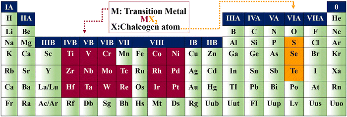
A great deal of research has been conducted on single-layer two-dimensional materials since the discovery of single-layer graphene a few years ago.1,2 As a result of this interest, both known and new 2D materials were discovered, including metal dichalcogenides and boron nitrides. The creation of optical devices based on 2D materials has advanced significantly. Optoelectronic devices have shown impressive performance with the introduction of TMDCs, including strong photoluminescence, a high current ON–OFF ratio, and acceptable carrier mobility as detailed in Table 1.3 Since unsaturated d-orbital transition metals are present in TMDCs, they can vary from semiconductors to semimetals:4 MoS2, WS2, selenium (Se) based TMDCs like MoSe2 and WSe2, and tellurium (Te) based TMDCs like MoTe2 and WTe2.5,6 The type of metal and chalcogen atoms employed can affect the characteristics of TMDCs. TMDCs, like MoS2 and WS2, have a layered structure with a metal atom sandwiched between two chalcogen atoms and only one or a few atomic layers of thickness.7Fig. 1 shows the periodic table highlighting the possible metals and chalcogens to form 2D TMDCs.8 The study of photodetection is one of the most promising fields for TMDC research. Photodetectors are tools that turn light into electrical signals. They have a wide range of uses in fields like sensing, imaging, and telecommunications.9 Because of their many benefits, self-powered photodetectors are crucial in the field of optoelectronics. By capturing and transforming incident light into electrical power, they provide energy-efficient solutions by lowering the need for external power sources like batteries and boosting energy efficiency.10 By reducing electrical waste and the carbon footprint, this not only increases the operating life of electronic products but also supports environmental sustainability goals. Greater convenience in mobility can be achieved by the development of wearable, lightweight, and portable devices, which are made possible by these detectors.11 Additionally, they are useful in difficult and distant locations where traditional power sources might not be available. TMDCs possess the capability to generate multiple excitons upon absorbing a single photon of light with energy exceeding the forbidden gap of materials. Photodetectors utilizing heterojunctions such as SnSe2/MoS2, MoSe2/WSe2, and WSe2/MoS2 have demonstrated inherent self-driven photo-switching capabilities.12 Jing Zhong et al. demonstrated that a photodetector utilizing a 9.5 nm thick α-MoSe2 thin film achieves the highest photocurrent of 4.60 μA, a photo-to-dark current ratio (PDCR) of 3067, and a photoresponsivity of 0.94 mA W−1 at zero bias.13 MoS2-based photodetectors exhibit elevated photoresponsivity and rapid photo response speed, and their photon absorption is predominantly confined to the UV-visible region. This constraint arises from MoS2's wide bandgap, approximately 1.83 eV for monolayer MoS2, limiting its utility in broadband photodetection.14 Near-infrared the (NIR) photodetectors have significant importance in various military and civilian domains, encompassing optical telecommunication, target imaging, remote sensing, time surveillance, and environmental monitoring. Given its relatively small bandgap, PtSe2 shows promise for potential applications in NIR detection.15 2D TMDCs emerge as promising candidates for ultralow-intensity photodetection. Nevertheless, the performance of these photodetectors is often hindered by rapid degradation induced by ambient conditions and slow response due to long-lived charge trapping, resulting in a substantial persistent photocurrent upon switching off the light source. To address these challenges, the functionalization of TMDCs with other materials is explored. Krishna Murari et al. developed a device using this approach by presenting an ITO/WSe2/SnSe2-based device that exhibits responsivity exceeding 1100 A W−1 and achieves a rapid transient response time on the order of 10 μs.16 The strong spin valley coupling feature of TMDCs represents a strong coupling between the spin and valley states of charge carriers, presenting significant benefits. It improves light–matter interactions and allows for the exact control and modification of these carriers in response to external stimuli, leading to better light absorption and photo response. A critical property of 2D materials such as TMDCs is carrier mobility, which can affect the performance of electronic components such as transistors and photodetectors.17 Comparing TMDC materials to their bulk counterparts, significant carrier mobility is common. This is because smaller dimensions of the material result in less scattering of electrons and holes by phonons, impurities, and defects. Furthermore, the TMDCs' comparatively low dielectric constant makes it possible for electrons and holes to interact with one another more strongly, which improves their mobility.18 Yet, several elements, including impurities, and the presence of a substrate, can have an impact on carrier mobility in TMDCs. Impurities, flaws, or a substrate can serve as electron and hole scatterers and lower carrier mobility.19 Moreover, the type and thickness of a particular TMDC can affect the carrier movement. For instance, although other TMDCs like MoSe2 and WSe2 have lower electron mobility, MoS2 and WS2 have comparatively high electron mobility.20 High-speed electrical devices and high-performance optoelectronic devices like photodetectors can both benefit from the high carrier mobility of TMDCs.21 To obtain high carrier mobility and maximize their performance in electrical and optoelectronic devices, quality and purity of TMDC materials must therefore be under good control.17,21 TMDC materials are highly reactive and ideal for use in catalytic and sensing applications because of their huge surface area to volume ratio.22 Electrons may pass through 2D materials with ease because of their high electron mobility. Due to this characteristic, TMDC materials can be used in electrical components like transistors and field-effect transistors.23 Due to the reduced dimensionality of the materials and their comparatively low dielectric constant, which permits a higher Coulomb interaction between electrons and holes, this feature results.24 The exciton binding energy of monolayer WS2 is large (0.7 eV).25 For MoS2, MoSe2, WS2 and WSe2 semiconductors, the theoretically expected carrier mobilities are significant (354, 269, 1739, and 1083 cm2 V−1 s−1 for each semiconductor).24 2D TMDCs have comparatively low hole mobility compared to their great electron mobility. Strong Coulomb interactions between holes, which result in a higher scattering rate and a lower mobility, are to blame for this.26 Due to their low dimensionality and high excitonic binding energy, 2D materials have a strong light–matter interaction. Due to this characteristic, 2D materials can be used in optoelectronic components like solar cells and photodetectors27,28 as shown in Table 2. TMDCs have strong light absorption properties and can absorb up to 5–10% of incident sunlight in as little as 1 nm of thickness, several orders of magnitude higher than that of Si and GaAs.29 An excellent example of this is a monolayer MoS2 photodetector which can have a photoresponsivity of 880 A W−1.30 Due to the anisotropic nature of 2D TMDCs' transport capabilities, multiple transport behaviors may be seen depending on the direction in which a material is measured. 2D TMDCs' electronic characteristics can be adjusted using this anisotropy to tailor them to certain uses. Transport features of 2D TMDCs are temperature-dependent, which means that as the temperature changes, so can the behavior of the devices. If the temperature drops, for instance, the electron mobility of 2D TMDCs typically rises while the hole mobility falls.31 A substantial anisotropy in the electrical and optical characteristics of TMDC materials can result from broken inversion symmetry, and this anisotropy affects the behavior of the material.32 TMDC materials have a large excitonic binding energy, causing the creation of excitons to result in a significant absorption of light (bound electron–hole pairs). It is possible to exploit this attribute to modify the optical characteristics of TMDC materials. 2D TMDCs
exhibit a quantum confinement effect, which means that the materials' reduced dimensionality affects transport characteristics of the material. The electronic band structure and electronic density of states may change as a result of these quantum confinement effects, which may change the transport properties of the material.33 Other types of scattering, such as scattering by phonons, impurities, and defects, can also have an impact on the transport characteristics of 2D TMDCs. These scattering processes have the potential to change the electrical band structure as well as the mobility of carriers. Because of their many unique qualities, these materials may be used in a wide range of applications in electronics, optoelectronics, and spintronics. These qualities may be controlled and altered by varying the synthesis conditions, material thickness, and the kind of metal and chalcogen atoms used. These properties are essential for comprehending the electronic behavior of 2D TMDCs and enhancing their performance in electrical devices.
Table 1 Advantages of TMDCs for self-powered photodetectors
| Advantages of 2D TMDCs for self-powered photo-detectors |
Explanation |
| High electron mobility |
TMDCs have high carrier mobility with a crucial property for high-speed transistors. MoS2 exhibits intrinsic mobility of around 1 cm2 V−1 s−1 when lacking high k dielectric gate materials. Incorporating HfO2 as the top-gate layer significantly boosts this value to a promising ∼150 cm2 V−1 s−1 at room temperature.37 |
| Mechanical flexibility |
TMDCs with high mechanical flexibility empower the photodetector to form curved surfaces, expanding its adaptability for various applications such as conformal imaging devices and wearable electronics. |
| Thermal conductivity |
The absorption of photons by the material, coupled with phonon interactions, can increase the temperature of the photodetector, inducing a conductivity change. For TMDC-based photodetectors operating exclusively in the NIR and visible spectral regimes, this effect is likely negligible.38 |
| Strong spin valley coupling |
The advantageous presence of robust spin valley coupling of TMDCs enhances the sensitivity and effectiveness of photodetectors significantly. |
| Wide range of optical properties |
Enhanced photodetection efficiency can be readily attained through the integration of TMDCs with other semiconductors, resulting in increased optical absorption and improved charge separation |
| Band gap |
TMDCs’ variable band gaps play a key role in the absorption of light, exerting a direct influence on their optical characteristics. |
| Transparency |
The majority of monolayer TMDCs exhibit optical transparency, having 85% transmission, with light absorption levels in the range of 5% to 10% within the visible range. |
 |
| | Fig. 1 Periodic table highlighting the possible metals and chalcogens to form 2D TMDCs. | |
Table 2 Carrier mobility of transition metal dichalcogenides (TMDCs) compared with wide bandgap semiconductors such as ZnO, GaN, Ga2O3, AlN, ZnS, GaAs, etc.
| Materials |
Charge carrier mobility (cm2 V−1 s−1) |
Ref. |
| ZnO |
137 |
58
|
| GaN |
800 |
59
|
| βGa2O3 |
150 |
60
|
| AlN |
300 |
61
|
| ZnS |
100–300 |
62
|
| GaAs |
1150 |
63
|
| MoS2 |
50–200 |
64
|
| ZrTe2 |
1.8 × 10⁴ at 2 K |
65
|
| ZrSe2 |
2316 at room temperature |
66
|
| ZrS2 |
1250 |
67
|
| HfS2 |
1800 |
68
|
| HfSe2 |
>2000 |
69
|
| NbS2 |
2.68 × 10³ |
70
|
| TaTe2 |
1400 |
71
|
| WSe2 |
1000 |
72
|
| MoTe2 |
200 |
73
|
| WS2 |
100 |
74
|
Transition metals and chalcogen atoms are shown in Fig. 1 by highlighted colors. Materials based on the four group IV(d2), V(d3), VI(d4), and VII(d5) metals form a layered structure, while non-layered materials are usually derived from the eighth group VIIIa–VIIIc (d6–d8) metals. It is easy to modulate the photoelectric response of TMDCs, regardless of the semiconductor or near metal they are made from. The number of layers in TMDC materials influences their optical properties based on their energy band structures. Since nanopores based on the atomically thin medicine of TMDCs may give a quick, accurate approach for high-resolution DNA sequencing, it has been demonstrated that TMDCs offer great potential for biophysical applications, including DNA sequencing and personalized medicine.19 A photodetector is a device capable of transforming an electrical signal into an optical signal. In recent times, numerous researchers have made significant advancements in the field by creating photodetectors that rely on transition metal dichalcogenides. In 2017, Wenzhi Yu et al. introduced near-infrared photodetectors that utilize a MoTe2/graphene heterostructure, and these photodetectors exhibit remarkable performance matrices, including a notably high responsivity of approximately 970.83 A W−1, a substantial photoconductive gain of 4.69 × 10⁸, and an impressive detective value of 1.55 × 1011 cm Hz1/2 W−1.34 In 2019, Pratik Pataniya et al. introduced a paper-based flexible photodetector that has enhanced the functionalization of WSe2 nanodots. This photodetector demonstrates an outstanding response time of 0.68 s. Additionally, it boasts a high responsivity value of 17.78 mA W−1, along with a detectivity of 5.68 × 10¹⁰ Jones.35 The majority of photodetectors necessitate an external power source to facilitate the movement of the charge carrier. Unfortunately, this requirement contributes to the enlargement of the overall device size and enforces a dependence on additional external equipment. Self-powered photodetectors represent a category of devices that operate without the need for an external power supply. These photodetectors have the potential to hold significant importance in applications such as the Internet of Things and optical sensor networks.36
This review aims to comprehensively estimate the performance, characteristics, and applications of self-powered photodetectors based on TMDCs. Additionally, it identifies current challenges and outlines future prospects for this promising technology. The properties of TMDCs that make them suitable for self-powered photodetectors have been explained, along with an exploration of how these properties can be enhanced through various functionalization strategies. It explores into the optical, electrical, and electronic properties of TMDCs and explores their societal impact. To gain a better understanding and enhance the overall performance of the photodetector, we provide an in depth explanation of the device structure of the self-powered photodetector and how these materials are used in different types of photodetectors like phototransistors and photodiodes. Additionally, we have presented various TMDC-based self-powered photodetectors, organized in table form, highlighting their parameters.
2. Need for self-powered photodetectors
Photodetectors are devices which transform light into an electrical signal. Self-powered photodetectors represent a novel category of photodetectors that facilitate photodetection without relying on external power sources.39 This concept has gained momentum due to the increasing popularity of wearable photodetectors. They are utilized in numerous fields, such as data storage, sensing, imaging, and communications. The capacity of photodetectors to detect light with high sensitivity and low noise is one of their key features.7,27,31 To detect and enhance light signals conveyed across optical fibers, photodetectors are employed in fiber-optic communication systems. Digital cameras, camcorders, and other imaging equipment employ photodetectors to turn light into an electrical signal that can be processed and saved as an image.40 UV communication has significant advantages over optical wireless communication methods due to its inherent benefits of resistance to interference and interception. It appears that using self-powered photodetectors as optical receivers will improve the integration and mobility of UV communication systems.41 A variety of sensing applications, including gas sensing, environmental sensing, and biometric sensing, use photodetectors.42,43 Flexible self-powered photodetectors are a significant component of flexible self-powered electronic systems, encompassing biosensors, nanogenerators, and photodetectors. Notably, these systems operate without the requirement for external energy sources, utilizing the photovoltaic effect even at zero voltage. This eliminates the necessity of developing a supplementary power supply system.44
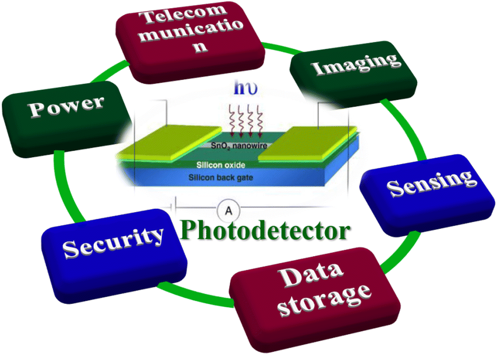
Photodetectors are used to read and write data on data storage devices such as CDs, DVDs, and Blu-ray discs. Using graphene, Mohit et al. developed photon-triggered, self-biased electronic circuits in 2021.45 These circuits included a variety of parts, including switches, transistors, logic gates, and lateral p–n and n–p homojunctions. Local probe measurements validated these advances.45 To transform X-ray and gamma-ray photons into an electrical signal, photodetectors are employed in medical imaging devices like X-ray and CT scanners. Photodetectors are utilized in systems like motion sensors and burglar alarms. Photodetectors are used in spectroscopy to find the light that a sample emits or absorbs. Self-powered ultraviolet photodetectors hold immense promise in optical communication, smart security systems, and space exploration by enabling photodetection without the need for external power sources. In conclusion, photodetectors are crucial components of contemporary technology. From Fig. 2, we can see that they are widely utilized in a variety of applications that call for the detection and conversion of light into an electrical signal. 2D TMDCs have been investigated as photodetectors due to their unique optical and electrical properties, such as their high absorption coefficient, high on/off ratio, and high responsiveness.46
 |
| | Fig. 2 Applications of TMDC photodetector devices. | |
3. Current challenges and potential solution to address these challenges in TMDCs for photodetectors
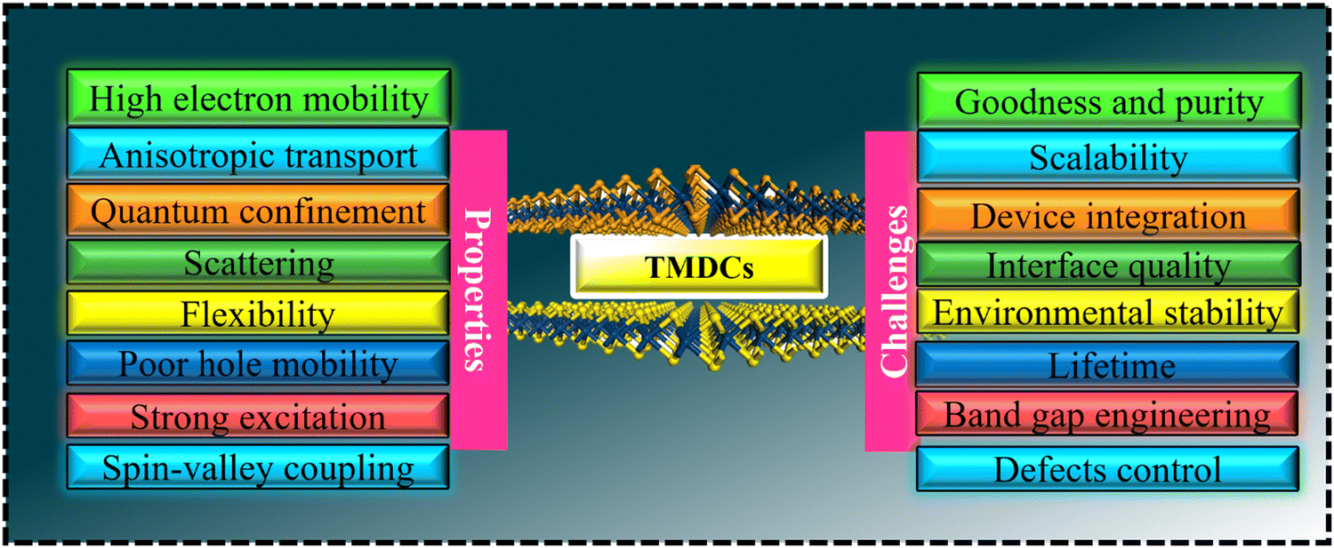
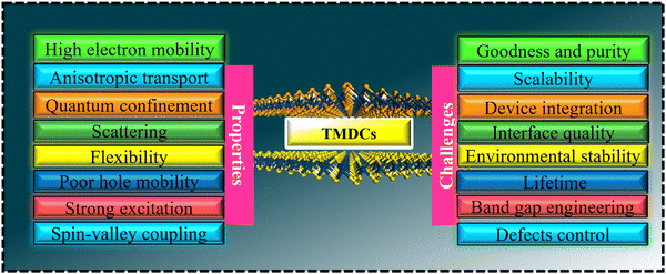
Photodetectors must be able to recognize weak signals while using the least amount of power possible.47Fig. 3 represents the properties and challenges associated with TMDCs. Photodetectors must be able to detect a variety of light intensities without being saturated. Also, they recognize and react to quickly changing lighting conditions. Photodetectors must be able to function under a variety of circumstances without deteriorating over time. Researchers are creating new kinds of photodetectors that may perform better than conventional silicon-based devices. Examples of these include those based on novel materials. For mass manufacture and commercialization, photodetectors must be reasonably priced and cost-effective.48 TMDCs can be readily synthesized by mechanically transferring and stacking various combinations of TMDC material heterojunctions. The absence of lattice mismatch issues, attributed to the van der Waals forces between layers, coupled with a more complex energy band structure, enhances the potential of photodetectors based on TMDC heterojunctions, offering extensive application possibilities. To enhance the photocurrent, the conductivity of TMDCs can be elevated through methods such as doping or creating heterojunctions with compatible conductive materials. Enhancing the photoluminescence intensity and quality of monolayer TMDCs presents a noteworthy challenge, critical for achieving low threshold lasers and high quantum efficiency LEDs. The examination of excitonic dynamics, which shows the fundamental mechanisms leading to excitonic formation and emission processes, is considered an effective tool for evolving the optical properties of TMDCs.49 Conventional photodetectors employing photosensitive materials face several challenges, including lattice mismatch, complex engineering processes, difficulties in incorporation with complementary metal oxide semiconductor devices, issues of toxicity, and high costs.50 The discovery and utilization of TMDCs in optoelectronic devices have prompted the development of a growing array of photodetectors using these materials. These advancements, enabled by diverse technology, have showcased outstanding performance skills.
 |
| | Fig. 3 Properties and exciting challenges associated with TMDCs. | |
4. Properties of TMDCs relevant to self-powered photodetectors
4.1. High carrier mobilities
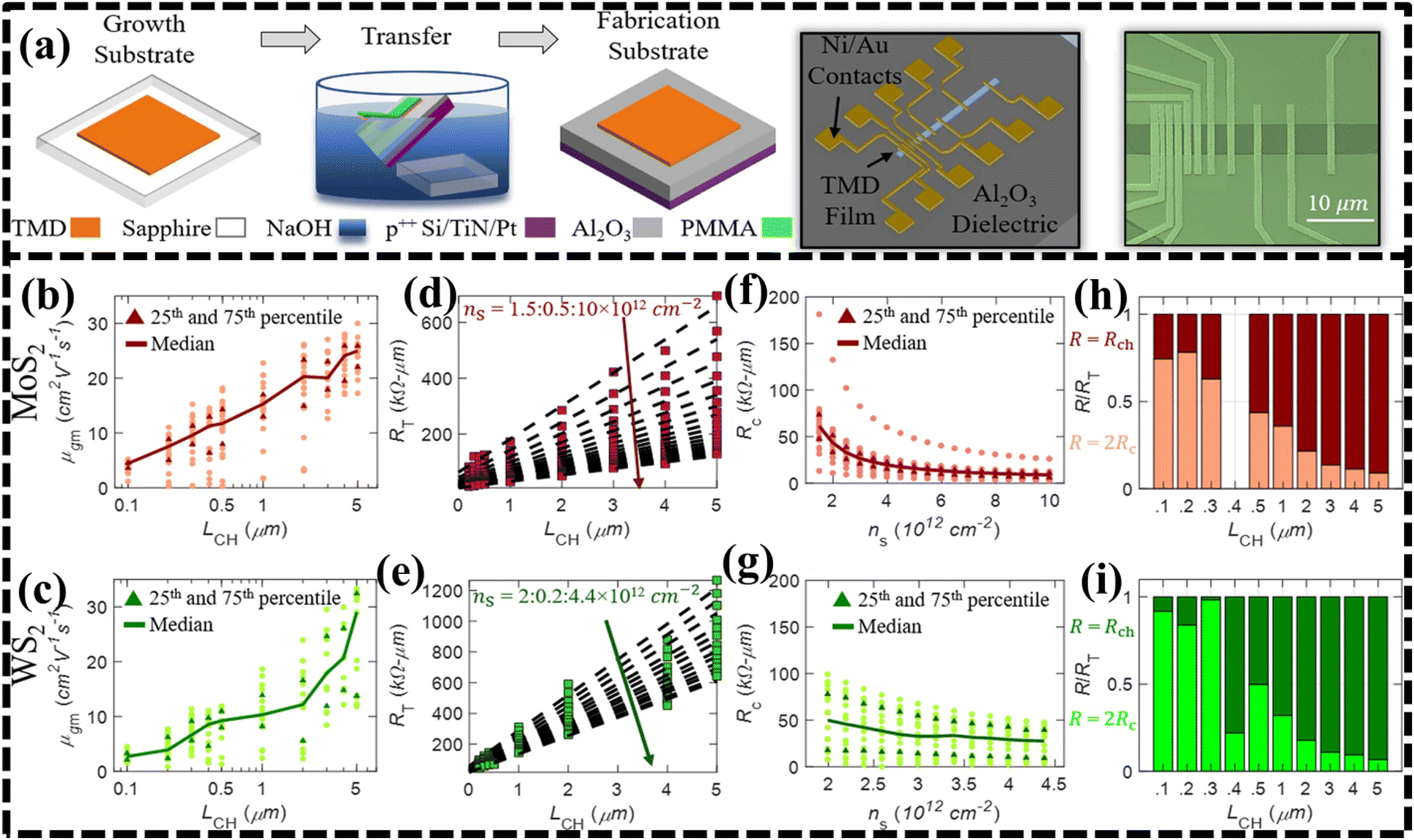
TMDCs with high carrier mobilities are essential for self-powered photodetectors because they facilitate effective charge transport, minimize carrier recombination, improve responsivity, speed up response times, and reduce noise, all of which improve signal-to-noise ratios.51,52 Together, these characteristics make photodetectors extremely responsive, sensitive, and able to precisely transform incident photons into electrical signals. They are therefore ideal for many uses, including optical communication, sensing, and imaging systems. Carrier mobility, which gauges how quickly electrons or holes may pass through a substance, is a critical component in determining how effectively electrical devices work.53 In 2D TMDCs, the carrier mobility is influenced by impurities as well as the strength of the contacts between the carriers and the lattice of the material.54 Due to the presence of a suitable bandgap in the material, 2D TMDCs typically have substantially higher carrier mobility than other two-dimensional materials like graphene. High on/off ratios are produced in field-effect transistors as a result, enabling effective field-effect control of the carrier density. Reduced impurities and defects in the material as well as the use of substrates with high levels of crystalline perfection can further increase the carrier mobility of 2D TMDCs. For instance, minimizing the contact between the 2D material and the substrate by employing hexagonal boron nitride (h-BN) as a substrate can dramatically increase the carrier mobility of MoS2.55 For 2D TMDCs, the maximum carrier mobility reported is typically in the range of 104 cm2 V−1 s−1 for MoS2, WSe2, and MoSe2 and 103 cm2 V−1 s−1 for WS2.56 These values are far greater than those of other 2D materials like graphene, but they are still less than those of traditional semiconductors like silicon and GaAs. Carrier mobilities of some TMDCs are given in Table 2. It is important to note that temperature, humidity, and strain can all have an impact on how mobile TMDCs are. The quality of the samples also plays a role; samples developed using MBE or CVD typically have higher mobilities than samples grown using exfoliation or solution-based techniques.5,24,33Fig. 4(a–c) depict the distribution of mobility derived using peak transconductance for various channel widths of MoS2 and WS2, respectively. The schematic depiction of PMMA (poly methyl methacrylate) aided wet transfer of monolayer TMDC is shown together with its device construction and SEM picture.57 When the channel width is scaled from 5 μm to 100 nm, the mobility of both materials varies from 23.9 cm2 V−1 s−1 to 3.6 cm2 V−1 s−1 for MoS2 and 29 cm2 V−1 s−1 to 2.7 cm2 V−1 s−1 for WS2. Both materials display considerable reliance on the channel width. For MoS2 and WS2, Fig. 4(d and e) display the total resistance with respect to the channel width, and Fig. 4(f and g) display the distribution of contact resistance. Contact-gating is responsible for a reduction in contact resistance with increased carrier density (nS), since the back-gate voltage modulates the Schottky barrier (SB) width at the metal/2D interface. The combined contribution of channel resistance and contact resistance with respect to channel width is shown in Fig. 4(h and i).
 |
| | Fig. 4 (a) Schematic representation of PMMA assisted wet transfer of monolayer TMDCs with their device structure and SEM image. (b) and (c) Distribution of mobility extracted using peak transconductance for different channel widths of MoS2 and WS2. (d) and (e) Total resistance with respect to the channel width for MoS2 and WS2. (f) and (g) Distribution of contact resistance for MoS2 and WS2. (h) and (i) Total contribution of contact resistance and channel resistance with respect to the width of the channel. Reprinted with permission from ref. 57 Copyright of Nature 2021. | |
4.2. Mechanical flexibility
Mechanical flexibility is crucial for self-powered photodetectors for a number of reasons. Firstly, it enables the photodetector to adapt to curved or uneven surfaces, which increases its versatility for a range of uses, including conformal imaging devices and wearable electronics.75 The ability of photodetectors to withstand mechanical stress or strain during handling or operation can be enhanced by mechanical flexibility. For flexible displays and medical sensors, for instance, where the photodetector may be twisted or stretched, this characteristic is quite helpful.76,77 All things considered, mechanical flexibility is an essential characteristic that raises the robustness and potential uses of photodetectors that run on their own energy. 2D TMDCs are known for their mechanical flexibility,78 or their capacity to bend and deform without breaking.79 Weak van der Waals interactions between layers of the material are to blame for this characteristic. By evaluating the flexibility of products created from the material, such as transistors or solar cells, it is possible to determine the mechanical flexibility of 2D TMDCs. The bending radius or maximum strain that these devices can sustain before breaking or performing poorly is often used to gauge their flexibility. Thinner layers are more flexible than larger ones, hence the mechanical flexibility of 2D TMDCs is also correlated with their thickness.80 For instance, although multi-layer MoS2 can withstand up to 0.5% strain, a single-layer MoS2 has been claimed to be flexible up to 1.5% strain.81 The WSe2 photodetector with graphite electrodes and h-BN encapsulation is schematically shown in Fig. 5(a). The optical image of the device is shown in Fig. 5(b), and the HR-TEM cross-sectional image is shown in Fig. 5(c). The illumination of the light on the WSe2 photodetector is shown in Fig. 5(d). Yixuan Zou et al. investigated the photoelectric properties of WSe2 photodetectors.82 The Ids–Vgs transfer curve changed higher over a range of gate bias values when exposed to white light at 20 °C, showing positive photoconductivity (PPC), as seen in Fig. 5(e). Remarkably, white light at 400 °C shifted the transfer curve to the left, with the shift increases with increasing light intensity; this is seen in Fig. 5(f). PPC was more prevalent in the N branch compared to NPC (negative photoconductivity) in the P branch. At 400 °C, Ids rose by setting Vgs at 3 V, converting the WSe2 device into a PPC photodetector (Fig. 5d). On the other hand, Ids dropped at 0 V, indicating that it was an NPC photodetector (Fig. 5e). The substrate on which the material is formed and the technique utilized to manufacture the material can both have an impact on the mechanical flexibility of 2D TMDCs. For instance, flexibility can be increased by growing it on a flexible substrate like polyethylene terephthalate (PET).81 A wide variety of flexible electronic applications, including flexible sensors, displays, and energy storage devices, can benefit from the mechanical flexibility of 2D TMDCs.83 Furthermore, stretchable and wearable electronic devices can be created using flexibility of TMDCs. It is important to note that building heterostructures of TMDCs, where the mechanical characteristics of the layers may be modified by altering the composition of the layers, can also improve the mechanical flexibility of TMDCs.
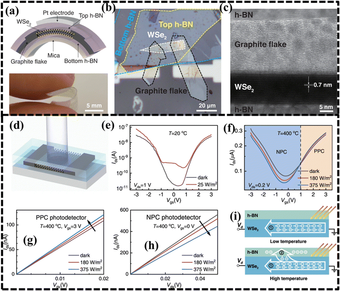 |
| | Fig. 5 (a) Schematic view of the WSe2 photodetector with h-BN encapsulation and graphite electrodes. (b) Optical image of the device. (c) HR-TEM cross-sectional image of the device. (d) WSe2 photodetector under illumination. (e) Ids–Vgs characteristics under dark and illumination at 20 °C. (f) Ids–Vgs characteristics under dark and illumination at 400 °C. (g) Ids–Vds characteristics Vgs = 3 V. (h) Ids–Vds characteristics Vgs = 0 V and at 400 °C. (i) Schematic view of the mechanism for the photodetection. Reprinted with permission from ref. 82 Copyright of Nature 2022. | |
4.3. Thermal conductivity
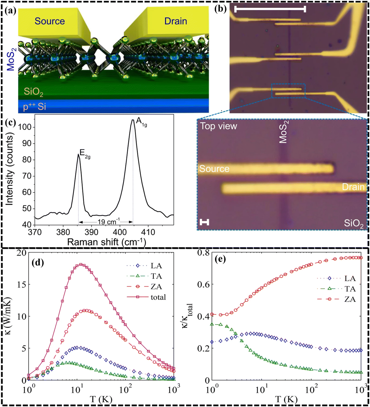
The characteristic that characterizes the capacity to conduct heat is called thermal conductivity. It affects how heat is dissipated during operation, which affects the device's thermal management. Maintaining the photodetector's stability and performance requires effective heat control. Elevated thermal conductivity can disperse surplus heat, averting overheating and possible harm to the apparatus.84 The photodetector's total energy efficiency may be impacted by thermal conductivity. High thermal conductive materials may effectively move heat away from the active areas of the device, minimizing energy losses from unintended heat dissipation and enhancing overall performance.85 Certain devices, like thermo photodetectors, may purposefully alter their heat conductivity in order to improve their functionality. These devices work by turning incoming photons into heat, which is subsequently recognized as an electrical signal. As seen in Fig. 6(a), FETs on CVD-grown monolayer MoS2 are constructed in a back-gated form. Fig. 6(b) depicts the back-gated transistor as it was manufactured. The Raman spectra show that the in-plane (E2g) and out-of-plane (A1g) Raman modes are separated by around 19 cm−1, as seen in Fig. 6(c). This is done to confirm that the channel is thick MoS2 in a single layer. Optimizing the efficiency of these detectors requires controlling the thermal conductivity. The internal phonon scattering processes in 2D TMDCs control the thermal conductivity of the substance.86 Due to the weak van der Waals forces holding the layers together, 2D TMDCs have a lower thermal conductivity than bulk materials. The out-of-plane thermal conductivity, which is typically in the range of 1–5 Wm−1 K−1, plays a major role in explaining the poor thermal conductivity of 2D TMDCs.87 Defects, contaminants, and strain can all be added to a material to further diminish its thermal conductivity. For thermoelectric applications, where a low thermal conductivity is sought to increase the thermoelectric figure of merit, this may be advantageous.88 Moreover, the crystalline quality can be increased, the number of layers can be decreased, and substrates with high thermal conductivity, like h-BN, can be used. It is important to note that temperature, humidity, and strain can all have an impact on the thermal conductivity of 2D TMDCs. The quality of the samples can also have an impact on the thermal conductivity of 2D TMDCs; samples developed by CVD or MBE often have higher thermal conductivities than samples formed by exfoliation or solution-based techniques. Guangqian Ding et al. investigated the Seebeck coefficient (S) for monolayer ZrSe2 and HfSe2 at various temperatures (400, 600, 800, and 1000 K).89 At lower temperatures, both materials show identical S values; however, a bipolar effect is seen at higher temperatures and lower carrier concentrations. Excitable electrons cause S peaks to drop and shift in the direction of increasing carrier concentrations. For a wide range of carrier concentrations, both materials show high S values (>200 μV K−1), with n-type S showing some slight superiority. Monolayer HfSe2 exhibits a higher S value of 660 μV K−1 at 600 K. Power factors indicate that n-type doping leads to improved thermoelectric performance, with HfSe2 beating ZrSe2. In the range of ideal carrier concentration, these power factors exhibit modest temperature dependency, suggesting that they are temperature-adaptable. While bulk ZrSe2 and HfSe2 show larger power factors with narrower band gaps and lower optimum carrier concentrations, monolayer MoSe2 and ZrSe2 have similar electrical transport capabilities. In Fig. 6(d), the thermal conductivities of the LA, TA, and ZA branches in WSe2 with a 1 μm size demonstrate a proportional relationship at low temperatures due to linear dispersion close to the Γ-point. However, at high temperatures, they exhibit a 1/T behavior that points to phonon–phonon scattering. Fig. 6(e) displays the contributions of spectral phonons to thermal conductivity in monolayer WSe2. The contributions of ZA phonons are the most prominent and increase with temperature. At room temperature, ZA phonons provide approximately 80% more than monolayer MoS2.
 |
| | Fig. 6 (a) Schematic diagram of a back-gated transistor. (b) Optical image of the photodetector device. (c) Raman spectrum of the MoS2 channel with a peak separation of 19 cm−1 confirming the monolayer. Reprinted with permission from ref. 90. Copyright of Nature 2023. (d) The temperature dependence of in-plane thermal conductivity of LA, TA and ZA branches of monolayer WSe2. (e) The relative contribution of spectral phonons to in-plane thermal conductivity in monolayer WSe2. Reprinted with permission from ref. 91 Copyright of Nature 2015. | |
4.4. Strong spin-valley coupling
For materials such as TMDCs, strong spin-valley coupling is an essential characteristic, especially in the field of self-powered photodetectors.92 Strong spin-valley coupling is beneficial for creating extremely sensitive and effective photodetectors because of this feature as well as its potential for valleytronics applications and high quantum efficiency.93 Due to the reduced dimensionality of the material and the presence of a substrate in 2D materials, broken inversion symmetry can happen. Inversion symmetry breaking in 2D materials has significant effects on such electrical and optical characteristics.94 For instance, it results in a phenomenon known as a strong spin-valley coupling, where the degrees of freedom associated with spin and valley of an electron are closely connected. Due to the high levels of spin polarization and valley polarization produced by this strong spin-valley coupling, 2D materials are well suited for spintronic applications including magnetic memory and logic circuits. For instance, the electrical anisotropy of 2D materials can be exploited to regulate the functionality of electronic components like transistors and photodetectors.95 In conclusion, broken inversion symmetry is a crucial characteristic of 2D materials that may be exploited to tailor and control their electrical and optical characteristics for a variety of applications in electronics, optoelectronics, and spintronics.
4.5. Optical properties
In the field of self-powered photodetectors, optical characteristics play a crucial role in determining how materials interact with light.96 These characteristics include the bandgap energy, refractive index, photoluminescence, photoconductivity, absorption spectrum, nonlinear optical phenomena, and polarization sensitivity. Photodetectors' sensitivity to various light wavelengths may be precisely tuned by adjusting their bandgap energy and absorption spectrum, which makes them sensitive to certain light sources and applications.97 Optimizing light absorption with techniques like total internal reflection or antireflection coatings requires control over the refractive index. Moreover, photoluminescence may be used for sensitive light detection, and photoconductivity allows absorbed photons to be converted into electrical impulses. Advanced signal processing can be facilitated by nonlinear optical phenomena, and polarization sensitivity makes it possible to identify polarized light sources. Self-powered photodetectors require careful design and performance optimization of these optical features for a range of applications. For a variety of optoelectronic applications, the remarkable optical properties of MoS2, WS2, and MoSe2 have sparked a lot of interest.98 Because of their unique optical characteristics, these materials are interesting choices for a variety of optoelectronic applications, including solar cells, photodetectors, LEDs, and more. Because of strong absorption coefficients of MoS2 in the visible and near-infrared parts of the spectrum, it is a great option for solar cells and photodetectors. Because of its high excitonic binding energy, light is significantly absorbed, especially in the near-infrared range, and excitons are produced. Because of its intense photoluminescence (PL), MoS2 is also an excellent material to employ in light-emitting diodes (LEDs) and other optoelectronic devices. Polarization dependence and anisotropy enable it to have unique optical features. Two optical properties shared by WS2 and MoS2 include strong absorption in the visible and near-infrared spectra and a high excitonic binding energy leading to considerable light absorption. A further characteristic of WS2 that makes it a desirable choice for LEDs and other optoelectronic devices is its strong photoluminescence in the visible region. Strong anisotropy and polarization dependency, which are characteristics of its optical properties, allow for the customization of its optical behavior.99 Notably, because of its strong excitonic absorption in the near-infrared spectrum, WS2 is especially well-suited for near-infrared imaging and detection. MoSe2 performs exceptionally well in optoelectronic applications and provides a wide range of optical characteristics. Maciej R. Molas et al. reported room-temperature photoluminescence (PL) and reflectance contrast (RC) spectra of an exfoliated MoS2 monolayer before and after four successive bis(trifluoro methane) sulfonamide (TFSI) passivation such as shown in Fig. 7(a–c).100 The first passivation leads to a two-fold increase in PL intensity, a 30 me V blue shift of the A exciton emission line as in Fig. 7(a), and similar blue shifts in RC spectra for A- and B-exciton resonances, accompanied by increased intensity and reduced linewidth. These changes illustrate a significant impact of super acid treatment on the optical properties of MoS2. Fig. 7d displays normalized PL spectra obtained from distinctively dosed areas within a monolayer MoSe2 crystal. The green trace represents an unaltered region of the crystal, exhibiting distinct peaks at approximately 1.55 eV and ∼ 1.77 eV, corresponding to the A- and B-excitations, respectively.101 MoSe2, like MoS2 and WS2, has strong photoluminescence and a high excitonic binding energy, which make it useful in optoelectronic devices. Numerous methods, including chemisorption and physisorption doping, can be used to modify intensity of the photoluminescence and spectral properties. The material's optical band gap may change with temperature. Hsiang-Lin Liu et al. discovered that when temperature increased, the resonance linewidth and peak locations of A and B excitons in monolayer TMDCs expanded to lower energies.102 An exciton peak location was used to calculate the optical band gap, which is the amount of energy required to produce an exciton by optical absorption. Variations in chemical composition, including electronegativity, caused this gap to fluctuate. It dropped as the temperature increased. The Bose–Einstein model explains this redshift in the optical band gap with increasing temperature. The band gap of TMDCs ranges from 1.0 to 2.1 eV; presented in Table 3.
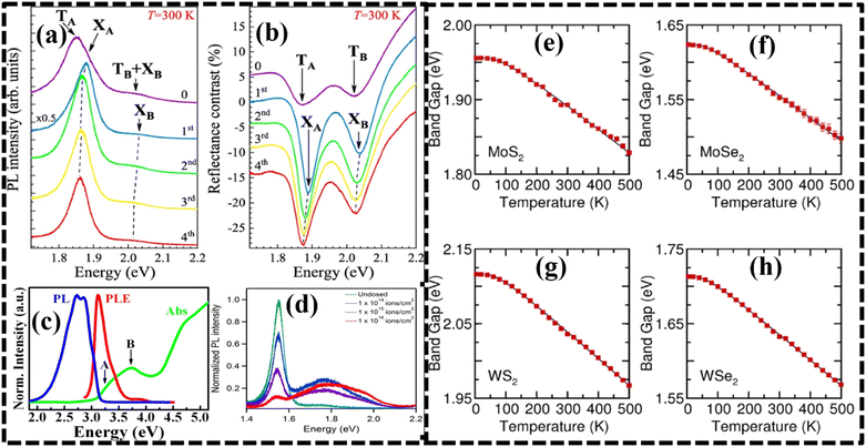 |
| | Fig. 7 Effect of successive bis(trifluoroethane) sulfonamide passivation on (a) photoluminescence and (b) reflectance spectra of the MoS2 monolayer. Reprinted with permission from ref. 100, Copyright of Nature 2019. (c) Photoluminescence (PL) photoluminescence excitation (PLE) and absorbance characterization of WS2. Reprinted with permission from ref. 103, Copyright of Nature 2019. (d) PL spectra of MoSe2 corresponding to the A exciton and B exciton. Reprinted with permission from ref. 101. Copyright of Nature 2016. (e)–(h) Temperature-dependent optical band gap of monolayer MoS2, MoSe2, WS2, and WSe2: spectroscopic ellipsometry and first-principles calculations. Reprinted with permission from ref. 102. Copyright of Nature 2020. | |
Table 3 The optical band gap of transition metal dichalcogenides104
|
|
S monolayer |
S bulk |
Se monolayer |
Se bulk |
Te monolayer |
Te bulk |
| Mo |
1.8–2.1 |
1.0–1.3 |
1.4–1.7 |
1.1–1.4 |
1.1–1.3 |
1.0–1.2 |
| W |
1.8–2.1 |
1.3–1.4 |
1.5–1.7 |
1.2–1.5 |
∼1.03 |
Metal |
| Ti |
∼0.65 |
∼0.3 |
∼0.51 |
Metal |
∼0.1 |
Metal |
| Zr |
∼1.2 |
∼1.6 |
∼0.7 |
∼0.8 |
∼0.4 |
Metal |
| Hf |
∼1.3 |
∼1.6 |
∼0.7 |
∼0.6 |
∼0.3 |
Metal |
| V |
∼1.1 |
Metal |
Metal |
Metal |
Metal |
Metal |
| Nb |
Metal |
Metal |
Metal |
Metal |
Metal |
Metal |
| Ta |
Metal |
Metal |
Metal |
Metal |
Metal |
Metal |
| Ni |
∼0.6 |
∼0.3 |
∼0.12 |
Metal |
Metal |
Metal |
| Pd |
∼1.2 |
∼1.1 |
∼1.1 |
∼1.3 |
∼0.3 |
∼0.2 |
| Pt |
∼1.9 |
∼1.8 |
∼1.5 |
∼1.4 |
∼0.8 |
∼0.8 |
4.6. Electronic properties
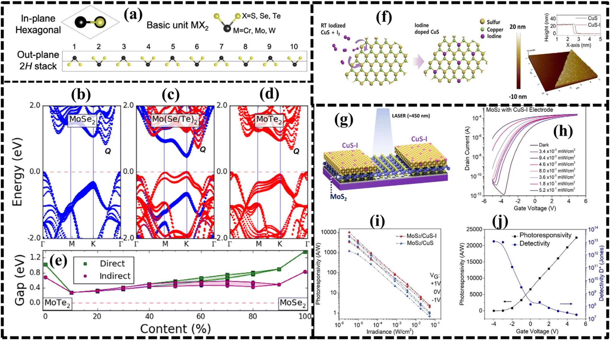
Fundamental characteristics of materials called electronic properties have a significant influence on the effectiveness and operation of self-powered photodetectors.105 These attributes cover a wide range of traits pertaining to the behavior of electrons, including energy levels, band structure, doping, recombination processes, carrier lifespan, electron and hole mobility, and density of states. Quantum efficiency may be maximized by comprehending recombination processes, and doping can be used to adjust conductivity and spectral sensitivity. Additionally, effective charge extraction and device design depend on an understanding of energy levels and band alignment. The development of high-performance self-powered photodetectors depends critically on tailoring these electrical features to the unique needs of photodetection applications. MoS2, WS2, and MoSe2 are examples of TMDCs, a family of materials recognized for their varied and useful electrical characteristics. For example, MoS2 has a distinct set of properties that affect its electrical conductivity, such as a band gap that is 1.8 eV for single-layer versions and 1.2 eV for multilayer ones. In addition, its high electron mobility allows for effective electron flow, which makes it a perfect fit for electrical components like transistors.106 Its strong light–matter interaction also makes it suitable for use in light-emitting diodes (LEDs) and photodetectors due to its low dimensionality and high excitonic binding energy. Because of its significant anisotropy, which allows for customization of its electrical and optical characteristics, MoS2 exhibits great potential in the field of spintronics.80 Similarly, band gaps and electron mobility are two electrical properties that WS2, another TMDC, has in common with MoS2.107 But unlike MoS2, WS2 shows a clear direct band gap of 2.0 eV for single-layer WS2 and an indirect band gap of 1.3 eV.77 Due to its high electron mobility, it may be used in electrical components such as field-effect transistors and transistors. Because of its high excitonic binding energy and low dimensionality, WS2 exhibits a strong light–matter interaction, making it suitable for use in LEDs and photodetectors. Similar to MoS2, WS2 has a strong spin-valley coupling and is adaptable for a range of applications due to its ability to change its electrical and optical characteristics depending on anisotropy. Furthermore, MoSe2, with its electrical characteristics, broadens the range of TMDCs. Electrical properties of MoSe2 are influenced by its direct and indirect band gap features. For a variety of applications, it is essential to comprehend these band gaps' locations and how they affect conductivity. Like its siblings, MoSe2 demonstrates anisotropy in its optical and electrical characteristics, significant spin-valley coupling, and light–matter interactions. All things considered, these TMDCs, MoS2, WS2, and MoSe2, with their particular and customized electrical properties, lead to a multitude of opportunities in electronics, optoelectronics, and spintronics, each providing special benefits and features for certain applications. As shown in Fig. 8(a), Xin-Gang Zhao et al.108 were systematically studied three forms of heterostructured superlattices [(A)n–(B)10-n]: type A, which consists of A and B with the same transition metal M but different chalcogens X; type B, which consists of A and B with the same chalcogen X but different transition metal M; and type C, which consists of A and B with distinct chalcogen X and transition metal M, within 10-layer periodic unit cell. Fig. 8(b) and (d) show the band structures of 10-layer stacked MoSe2 and MoTe2. These band structures show indirect bandgaps. Conversely, a [(MoSe2)2–(MoTe2)8] heterostructure is depicted in Fig. 8(c) that displays a direct bandgap at the K point, signifying a transition from an indirect to a direct bandgap. As seen in Fig. 8(e), direct bandgaps of 0.27 and 0.32 eV are obtained when n is 1 and 2 in [(MoSe2)n–(MoTe2)10−n]. Fig. 8(f) shows the schematic illustration of room temperature iodine-doped synthesis of CuS with their AFM surface topology. Taehun Kim et al. fabricated a CuS–I/MoS2 phototransistor with reduced contact barriers demonstrating enhanced phototransistor performance such as shown in Fig. 8(g).109 Its photoresponsivity exhibits a linear relationship with incident power and surpasses the CuS/MoS2 phototransistor under all gate biases (Fig. 8h–j). Notably, a high photoresponsivity of 2.25 × 10⁴ A W−1 is achieved, and a maximum detectivity (D*) of 1.16 × 10¹¹ Jones is attained under negative back-gate voltages.
 |
| | Fig. 8 (a) A schematic 10-layer unit cell to construct heterostructured superlattices, (b)–(d) band structure of MoSe2, (MoSe2)2–(MoTe2)8 and MoTe2 supercells, (e) direct and indirect band gaps depending on the content. Reprinted with permission from ref. 108, Copyright of Wiley 2020, (f) schematic illustration of room temperature iodine-doped synthesis of CuS with their AFM surface topology, (g) CuS-I/MoS2 phototransistor device, (h) drain current of the device, (i) the photoresponsivity of the device, and (j) photoresponsivity with respect to gate voltages. Reprinted with permission from ref. 109, Copyright of Wiley 2023. | |
5. Functionalization strategies to induce self-powered properties
By combining them, atom-thin TMDC materials may be produced separately and layered to create van der Waals-bonded heterostructures, which open up surprisingly new possibilities for functional devices.110 Functionalization means the modification of the surface and structure of these materials with various functional groups or molecules. Parameters of a photodetector such as responsivity and detectivity are enhanced in these materials after functionalizing them with other suitable materials. For TMDCs to be incorporated into future electronic devices, doping becomes a crucial first step.111
5.1. By doping
TMDC-based photodetectors using doping can be used to provide self-powered properties through optoelectronic behavior and electronic structure modification of the material.1 TMDCs may be doped to become either n-type (electron-donor) or p-type (hole-donor) by carefully adding certain impurities or foreign atoms. This will change their carrier concentration and produce an inherent potential. Because of its intrinsic potential, the photodetector can produce electricity on its own when light strikes it, making it a self-sufficient gadget that does not require an external power source.112 The required doping effects may be achieved by a variety of doping processes, including chemical vapor deposition, ion implantation, and chemical functionalization. This versatility makes TMDCs an excellent platform for the development of self-powered photodetectors with customized optoelectronic features. Noble metals are particularly advantageous due to their resistance to environmental corrosion and oxidation, making them ideal candidates for enhancing the properties of TMDCs.113,114 Stable doping is required for the incorporation of TMDCs into durable device manufacturing. Hu et al. verified that an electric field may adjust the Schottky barrier at the graphene/MoS2 interface, converting the n-type into the p-type and creating an Ohmic contact.115 A functionalized TMDC MoS2(1-x)Se2x/graphene heterostructure with excellent quality, tunable structure, and electrical characteristics was recently reported by Yue et al. This heterostructure is crucial for phototransistors.116 The electrical performance of monolayer MoS2 can be enhanced by Sm doping. It is done by an atmospheric pressure chemical vapor deposition method. Sm ions introduced in monolayer MoS2 led to an increase in the threshold voltage (from −12 to 0 V) for an Sm-doped MoS2 field effect transistor. Furthermore, by doping of Sm, the electrical performance of the FET has been improved by 500%, with a 40% increase in mobility of the FET.117 MXene nanoflake-doped WS2 has a five-fold increase in PL efficiency, which is higher than that observed with electrical or plasma doping.118 Ren-Jie Chang et al. reported the post growth alteration of WS2, which was grown through chemical vapor deposition.119 By employing a SnS precursor to introduce metallic Sn dopants, a variety of Sn/W/s composite 2D materials are produced. Fig. 9(a) reported by Shisheng Li et al. illustrates how substituting neighbouring elements (Re, V, or Nb) for the Mo and W atoms in group VI TMDCs can alter the electrical properties of the TMDCs.120 This substitutional doping affects the band structure and electrical characteristics of 2D TMDCs. The methods for making mixed salt solutions for doping are depicted in Fig. 9(b), starting with the preparation of source precursors (Na2MoO4, Na2WO4, NaReO4, and NaVO3). These are used to produce mixed salt solutions with precise control over the doping concentration, such as XReMo, XVMo, XReW, and XVW. Fig. 9(c) provides details of the synthesis of Re- and V-doped TMDC monolayers. These doped monolayers are created by sulfurizing or selenizing the mixed salts using an ambient-pressure thermal chemical vapor deposition (CVD) process, following the spin-coating of the mixed salt solutions onto sapphire substrates. Fig. 9(d and e) shows typical transport curves illustrating the electrical behavior of Re- and V-doped MoS2 and WS2 monolayers. Fig. 9(f) schematically depicts Au or Pd contacts and includes an optical image of the device that may display the experimental setup. Fig. 9(g) compares the transport characteristics of WS2 field-effect transistors (FETs) with those of Au, Pd, and V-doped WSe2 to provide insight into the electrical performance of these materials. The projected density of states (PDOS) of WSe2 monolayers is shown in Fig. 9(h), which shows details of the electronic structure of these doped materials.
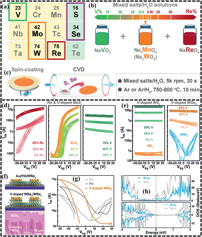 |
| | Fig. 9 (a) Partial periodic table showing substitutional Re and V doping to TMDCs, (b) mixed salt solutions with different NaReO4 and NaVO3, (c) spin coating and the conditions employed in the CVD growth of Re and V doped TMDC monolayers, (d) and (e) typical transport curves of Re and V doped MoS2 and WS2 monolayers, (f) schematic of Au or Pd contacts and optical image of the device, (g) comparison of transport properties of WS2 FETs with Au, Pd and V-doped WSe2, and (h) projected density of states (PDOS) of WSe2 monolayers. Reprinted with permission from ref. 120, Copyright of Wiley 2021. | |
5.2. Tuning by strain engineering
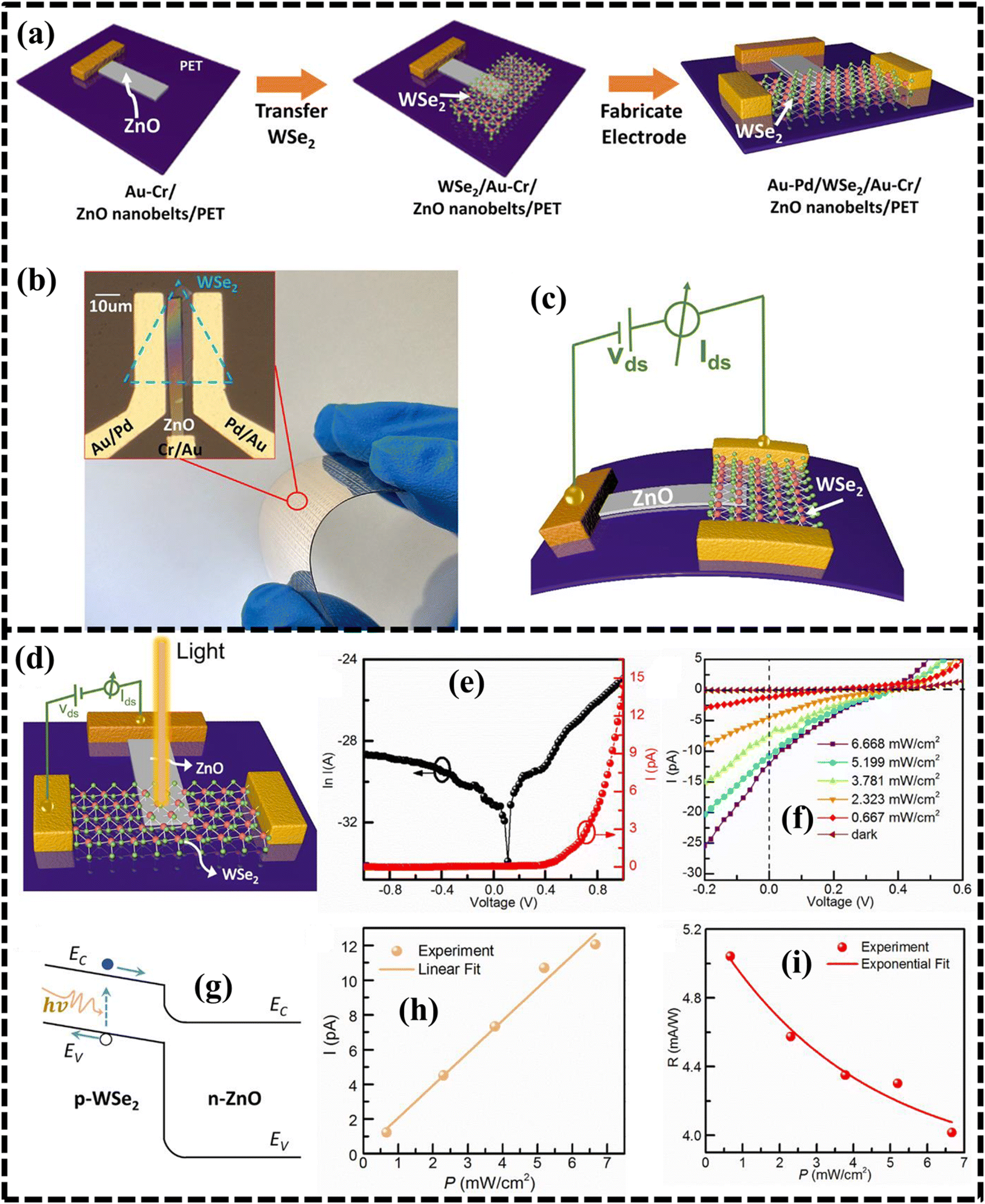
Applying strain engineering can also enhance the performance of self-powered photodetectors based on TMDCs.121 TMDCs' optoelectronic characteristics may be deliberately strained to maximize self-powered photodetection. Tensile strain may be deliberately used to raise the bandgap of TMDCs in self-powered photodetectors, increasing their sensitivity to particular light wavelengths.122 Higher photoresponsivity and spectrum selectivity can be attained as a result. Furthermore, by optimizing the strain, charge separation and transport mechanisms may be strengthened, increasing the photodetectors' self-sustainability and energy conversion efficiency.123 In order to modify TMDCs' characteristics for self-powered photodetection, strain engineering is essential. This allows researchers to create photodetectors that are not only light-sensitive but also capable of producing electricity from incident photons, which removes the requirement for an external power source. Strain in the crystal lattice modifies orbital interactions, coupling between neighboring atoms, and lattice constants to design the physical characteristics of a solid. The majority of early TMDC monolayers may have their electrical and magnetic characteristics changed by strain engineering, creating further opportunities for optoelectronic and spintronic applications down the road. Utilizing a CVD-grown technique for carrier mobility adjustment, strain control may be used to optimize 2D electronic devices. For group IVB TMDCs, the band gap rises with tensile strain; however, for ZrX2 and HfX2, the band gap begins to drop at strain, ranging from 6–8%.124 Group VB TMDCs can undergo ferromagnetism either because of tensile strain or because it enhances the existing ferromagnetism.124 With the exception of CrTe2, TMDCs experience a direct to indirect band gap transition upon application of the tensile strain group VIB.125–127 Frisenda's group investigates the short-term modulation of single-layer TMDCs' reflectance by biaxial strain. Calculations using density functional theory indicate that the electronic bandgap and other electrical characteristics of many early TMDCs are significantly influenced by the tensile strain. For group IV B TMDCs (TiX2, ZrX2, and HfX2), the increasing tensile strain causes the bandgap to grow, whereas for X = S, Se, the bandgap increases and begins to decrease.128 It has already been demonstrated that atomic layered TMDCs can be engineered by using a variety of strain-engineering strategies, such as mechanical bending using a flexible substrate heated with a focused laser or applying a different force on a monolayer of MoS2.129 MoS2 exhibits a high Young's modulus and has a much higher mechanical strength than many high-tensile materials. This makes MoS2 an ideal material for microelectronic applications.130 MoS2 is a promising microelectronic and straintronic material that can be manipulated by the application of strain to regulate its carrier density, effective mass, and mobility. Fig. 10(a) depicts the development of a flexible p–n photodetector by Junli Du et al. employing few-layer WSe2 and ZnO nanobelts.131 It provides a schematic representation of the steps involved in creating this photodetector as well as the arrangement of the materials and components. Fig. 10(b) displays an optical image of the flexible photodetector under tensile stress. An inset of this image displays a close-up of the photodetector. It provides the observer with a visual representation of the real device by displaying the electrodes, ZnO nanobelts, and few-layer WSe2. Fig. 10(c) provides a schematic illustration of the operation of the flexible p–n photodetector using the few-layer WSe2–ZnO nanobelt. It makes it easier to comprehend how the device transforms light into an electrical signal. Fig. 10(d) schematically displays the WSe2–ZnO photodetector installed on a flexible PET substrate along with the structural arrangement of the device. Fig. 10(e–i) displays the current–voltage (I–V) curves on both linear and logarithmic scales for the flexible WSe2–ZnO diode at 0% strain. These graphs give insight into the electrical behavior of the diode at various voltage levels as well as the I–V characteristics of the WSe2–ZnO photodetector at 0% strain under various optical light intensities.
 |
| | Fig. 10 (a) Schematic fabrication process of the p–n photodetector with a WSe2–ZnO nanobelt, (b) optical image of the device under tensile strain, (c) device operation mechanism of the photodetector device, (d) schematic diagram of the device on the flexible PET substrate, (e) current–voltage characteristics under 0% strain, (f) current–voltage characteristics under different illumination intensities, (g) photovoltaic effect mechanism for self-powered photodetector device, and (h) and (i) photocurrent and responsivity with respect to the illumination intensities. Reprinted with permission from ref. 131 Copyright of Elsevier 2019. | |
5.3. Surface functionalization
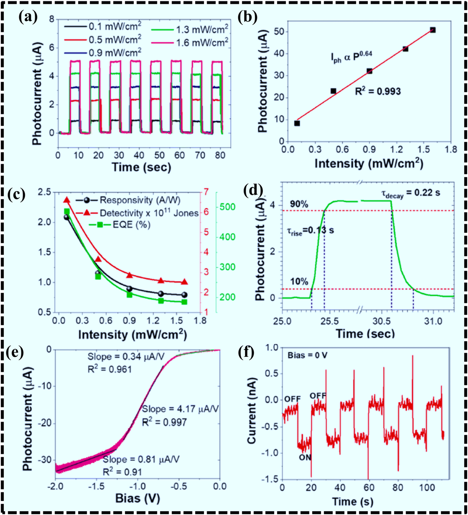
One key tactic in creating self-powered photodetectors based on TMDCs is surface functionalization.132 By changing their surface properties, such as WSe2 or MoS2, TMDCs can perform better in self-powered photodetection applications. Surface functionalization can be utilized to attach certain molecules or ligands, which will improve the TMDCs' interaction with incident light and boost their photoresponsivity and capacity to absorb light.133 Enhancing charge separation and transport by functionalization can also result in more effective energy conversion. Furthermore, TMDC-based photodetectors may be made more reliable and stable by surface functionalization, which improves their suitability for real-world uses. All things considered, surface functionalization in TMDCs is essential for adjusting their surface characteristics to produce extremely sensitive, self-powered photodetectors for a variety of optoelectronic uses. In donor/acceptor interfaces, PCT occurs as a result of photon absorption. In this way, PCT is linked to all other excited-state decay processes and is therefore kinetically related to their thermodynamics.134 Monolayer TMDC semiconductors are characterized by excitonic transitions of the Brillouin zone K point, which dominate with their optical and optoelectronic properties.135,136 TMDCs are capable of modulating excitonic transitions by altering their carrier concentrations, thereby controlling their optical properties.137 According to Jungwook et al. TMDCs can be modulated by chemical species adsorption. For example, when p-type dopants such as 2,3,5,6-tetrafluoro-7,7,8,8-tetracyanoquonodimethane (F4TCNQ) are interfaced with monolayer MoS2 and WS2, excess electrons are decreased from these TMDCs such that their PL intensity increases by reducing negatively charged excitons and thus enhancing excitonic recombination.138,139 When cesium carbonate (electron donating) is interfaced with monolayer MoS2, charge excitons are increased, such that PL intensity decreases.140 An examination of the photodetection characteristics of Ag–WS2/Si heterojunction-based devices at various power intensities is presented by Meswa Patel et al.141 The time-resolved photoresponse at a constant 2 V bias is shown in Fig. 11(a), which shows that current significantly increases upon illumination and drops upon turning off the light. Exciton production at the Ag–WS2/Si interface is responsible for this. As light intensity rises, photocurrent increases, as may be seen in Fig. 11(b). The photoresponse is limited by carrier entrapment, as given by the relationship of Iph ∝ P0.64. Fig. 11(c) shows the variations in detector parameters with light intensity. At 532 nm, 0.1 mW cm−2 illumination, and −2 V bias, the maximum of responsivity, detectivity, and external quantum efficiency (EQE) are reached. The time-resolved photoresponse, with measured τrise and τdecay, is displayed in Fig. 11(d). Because of biomolecular adsorption on defect sites, τdecay is somewhat greater, extending the lifespan of the charge carrier. Under white light, photocurrent fluctuation with bias voltage is shown in Fig. 11(e), in which photocurrent rises in three stages, linearly. The self-powered time-resolved photoresponse with notable photoresponsivity, detectivity, and EQE is displayed in Fig. 11(f) as a result of n-Ag–WS2 and p-Si forming a type-II interface and junction. Furthermore, the Ag–WS2/Si spectral photoresponse is compared to WS2/Si heterojunctions, demonstrating higher photocurrent values for Ag–WS2/Si, particularly at 532 nm because of Ag nanoparticle surface plasmon resonances.
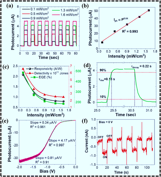 |
| | Fig. 11 (a) Time dependent photo response of the Ag–WS2 photodetector device at different illumination intensities, (b) photocurrent with respect to the illumination intensities, (c) responsivity, detectivity and EQE of the photodetector device, (d) rise and decay time constant, (e) photocurrent with respect to the applied bias potential and (f) time dependent photo response under an applied bias potential of 0 V. Reprinted with permission from ref. 141, Copyright of Elsevier 2021. | |
5.4. Covalent functionalization
A particular technique for surface functionalization of TMDCs is called covalent functionalization, which entails the creation of robust covalent connections between the functional groups and the TMDC surface.142 The optimization of TMDCs' performance in self-powered photodetection can be achieved by covalent functionalization. Covalent functionalization enables exact control over the insertion of certain molecules or chemical groups on the TMDC surface for self-powered photodetectors based on TMDCs. It is possible to modify these covalently bound groups to improve photoresponsivity, charge separation, and transport efficiency in addition to its light-absorbing capabilities.143 In photodetection applications, covalent functionalization offers a stable and long-lasting alteration of the TMDC surface, guaranteeing long-term performance and dependability. TMDCs' optoelectronic characteristics may be precisely tuned to increase their sensitivity to incoming light and their ability to produce electrical energy from absorbed photons by carefully attaching the right functional groups through covalent bonds. This strategy may result in the creation of self-powered, incredibly effective photodetectors with specialized performance traits. Duo O. Li et al. demonstrated the direct covalent functionalization of semiconducting MoS2.144 Mild chemistries are needed to allow for the direct covalent functionalization of semiconducting TMDC surfaces. It has been possible to covalently functionalize the basal plane of unaltered semiconducting MoS2 using moderate conditions and aryl diazonium salts. This allows for the covalent binding of a range of functional groups to the surface of MoS2.145
5.5. Non-covalent functionalization
An additional method for surface modification in TMDCs for self-powered photodetection is non-covalent functionalization.146 In this way, specific molecules or functional groups are linked to the TMDC surface by weaker, non-covalent interactions such as hydrogen bonds, van der Waals forces, or electrostatic interactions.147 Reversible changes and the preservation of TMDCs' inherent features are two benefits of non-covalent functionalization. Non-covalent functionalization enables accurate adjustment of the TMDC surface characteristics to improve its interaction with light in the context of self-powered photodetection. Adsorbed functional groups, such as organic compounds or polymers, can enhance the efficiency of charge separation, light absorption, and photoresponsivity on the TMDC surface. Increased photodetection sensitivity may result from this. Moreover, through charge transfer and other interactions at the interface, non-covalent functionalization might make it easier to assemble layered structures or heterostructures using TMDCs and other materials, which may increase photodetection performance. The reason for non-covalent functionalization is appealing is that it preserves the inherent characteristics of TMDCs and may be reversed, meaning functional groups can be added or removed as needed. With this flexibility, the structural integrity and electrical characteristics of TMDCs may be preserved while optimizing their qualities for self-powered photodetection. Non covalent interactions play a crucial role in customizing the characteristics of nanomaterials. The initial exploration of this concept was carried out with graphene.148 Subsequently, this approach was extended to inorganic counterparts, including black phosphorus and MoS2,149 as the representative of TMDCs. Noncovalent functionalization of TMDCs has primarily been achieved on surfaces, with only a few exceptions.150 Non-covalent molecular functionalization of materials revolves around properties arising from electrostatic forces, dipole–dipole interactions, induced dipole interactions, hydrogen bonding, and van der Waals forces. These methods of non-covalent interaction enable convenient surface modification without necessitating particular molecule–substrate bonds.151 In recent years, the scientific community has directed its focus toward molecular methods that intricately adjust the characteristics of 2D materials. This is achieved by harnessing the extensive range of available molecular systems. The integration of these materials with photo responsive molecular systems offers a captivating and demanding avenue, holding the potential for revolutionary technologies in multifunctional optoelectronic applications.152
6. Device structures for self-powered photodetector devices
6.1. Phototransistor devices
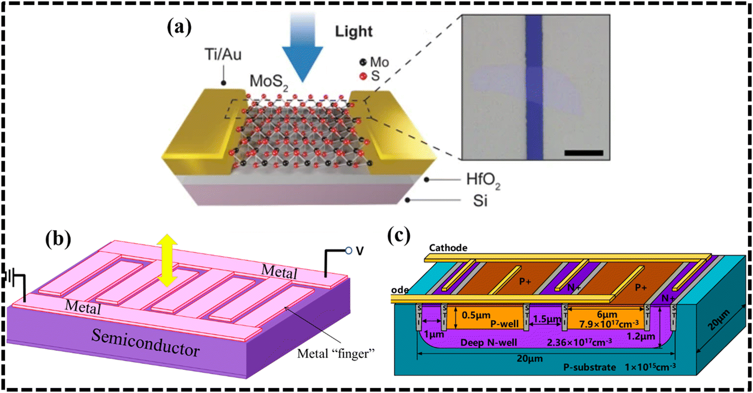
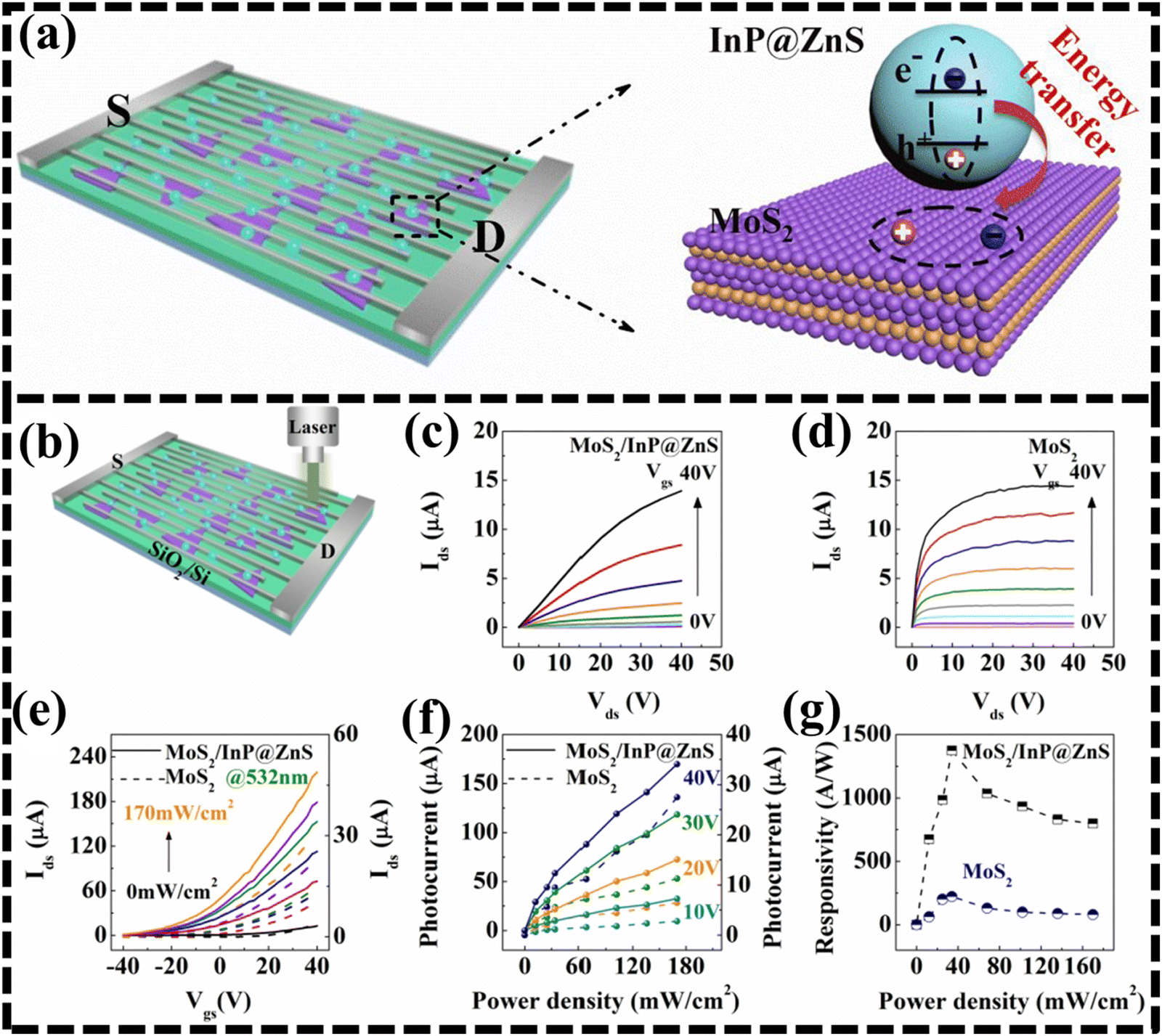
When used in phototransistor mode, bipolar junction transistors (BJTs) may be set up to function as self-powered photodetectors. Fig. 12(a) shows the high responsive MoS2 phototransistors based on charge trapping HfO2 dielectrics and Fig. 12(b) shows the avalanche photo diode, whereas Fig. 12(c) shows the integrated MoS2 phototransistors. Incident light causes electron–hole pairs to form in the base area, affecting the base current, while operating in the active zone, where the base-emitter junction is forward-biased. Consequently, this regulates the collector current, thereby increasing the photocurrent. Because they may give better gain and enhanced sensitivity when compared to solo photodiodes, phototransistors are highly valued for their intrinsic sensitivity to light. They are appropriate for applications needing quick light detection because of their comparatively quick reaction times. While BJTs do not produce energy on their own, they can be incorporated into systems that do, like photovoltaic cells or piezoelectric elements, to produce self-powered photodetectors that capture light and turn it into electrical signals for a variety of light-sensing uses. Bipolar junction transistors serve as the foundation for the type of photodetector known as a phototransistor (BJT). It has a light-sensitive area where the absorption of light creates electron–hole pairs, which in turn modify the current passing through the transistor. It is made up of a p–n–p or n–p–n type semiconductor structure. An intrinsic (i-type) semiconductor, an n-type semiconductor, and a p-type semiconductor make up the three layers of a phototransistor, a form of photodetector based on a bipolar junction transistor (BJT). An alternative to this device is a phototransistor based on 2D transition metal dichalcogenides (TMDCs), which uses 2D TMDC materials as the semiconductor layers. The n-type layer of a phototransistor made of 2D TMDCs is often made of a 2D TMDC material doped with impurities like phosphorus or nitrogen, whereas the p-type layer is typically made of a 2D TMDC material doped with impurities like boron or aluminum.153 Typically, the intrinsic layer is made of an impurity-doped 2D TMDC material. A light that enters the intrinsic layer of the phototransistor and is absorbed there produces electron–hole pairs that modify the current that passes through the component. Both the detection of light and the production of an electrical signal can be accomplished by modulating the current. The phototransistor based on 2D TMDCs offers many benefits, including high sensitivity, quick response times, and minimal noise. The device also has strong light–matter interaction and high electron mobility, which can improve its performance as a photodetector, thanks to the use of 2D TMDCs as the semiconductor layers. However, the phototransistor based on 2D TMDCs also has some constraints, such as the requirement to synthesize superior, homogenous 2D TMDC layers and the requirement to design the device structure and the doping. However, 2D TMDC-based phototransistors also have several drawbacks, including the necessity to construct high-quality, homogenous 2D TMDC layers as well as the need to design the structure of the device and doping levels to achieve good performance. These tools have been extensively employed in a wide range of applications, including sensing, imaging, and spectroscopy. They are also frequently utilized in the detection of electromagnetic radiation in the ultraviolet, visible, and infrared spectra as well as light-sensitive components in optical communication systems, such as fiber-optic networks. Kaixi Shi et al. present a comprehensive overview of an InP@ZnS–MoS2 hybrid energy transfer system and associated photodetector devices.154Fig. 13(a) offers a schematic representation of the energy transfer mechanism. Fig. 13(b) provides a structural diagram of the photodetector device, illustrating its physical layout. Fig. 13(c) and (d) show Ids–Vds characteristics for the InP@ZnS–MoS2 phototransistor and MoS2 phototransistor, respectively, under various backgated voltages, revealing their current responses to different voltage conditions. Fig. 13(e) displays the gating response (Ids–Vgs) for a fixed Vds, showcasing how current changes with gate-source voltage. Fig. 13(f) highlights the phototransistors' photocurrent as a function of laser power density, while Fig. 13(g) demonstrates the photoresponsivity of the phototransistors under specific voltage and gate conditions as a function of laser power, offering insights into their light-detection capabilities and performance.
 |
| | Fig. 12 (a) High responsivity in MoS2 phototransistors based on charge trapping HfO2 dielectrics,155 (b) avalanche photo diode,156 and (c) MoS2 phototransistors. Reprinted with permission from ref. 157. | |
 |
| | Fig. 13 (a) Schematic of the InP@ZnS-MoS2 hybrid energy transfer system, (b) a structural diagram of the photodetector device, (c) Ids–Vds characteristics under different backgated voltages for the InP@ZnS-MoS2 phototransistor, (d) Ids–Vds characteristics under different backgated voltages for the MoS2 phototransistor, (e) gating response (Ids–Vgs) for Vds = 1 V, (f) photocurrent of the phototransistors devices with laser power density and (g) photoresponsivity of the phototransistors at Vds = 1 V and Vgs = 40 V as a function of laser power. Reprinted with permission from ref. 154, Copyright of American Chemical Society 2020. | |
6.2. Heterostructured photodetectors
Innovative devices known as heterostructured self-powered photodetectors utilize the potential of mixing several semiconductor materials to enable improved light detection and self-sufficient functioning. These photodetectors have a thoughtfully constructed stack of several materials or layers, each selected for certain qualities. One of the semiconductor layers absorbs photons and produces electron–hole pairs when exposed to incoming light. Effective charge separation takes place at the interface between these materials, preventing these carriers from recombining. In order to convert the produced electron–hole pairs into electrical energy, the heterostructure can include energy-harvesting elements like solar cells or piezoelectric materials. Because of their clever design, which combines specialized materials and components for effective energy collecting and conversion, heterostructured devices are self-powered. Through the heterostructure combination of diverse semiconductor materials and energy conversion components such as thermoelectric modules, photovoltaic cells, or piezoelectric components, these devices can independently convert a variety of energy sources, including mechanical stress, light, and temperature gradients, into electrical power. Electrical current is produced when created electron–hole pairs do not recombine because of the intrinsic charge separation at material surfaces. Self-powered devices in the semiconductor sector are included in the study of Wanhui Wu et al.158 Epitaxially connected TMDCs' lateral heterojunctions show promise for self-powered devices due to their quick electron–hole separation. The photovoltaic light sensors based on the monolayer MoS2–WS2 in-plane heterostructure exhibit a spectral responsivity (Rλ) of 4.36 mA W−1 and a detectivity (D*) of 4.36 × 10¹³ Jones under 28.64 mW cm−2@532 nm. Because these devices use the inherent potential at the interface, they are interesting candidates for future applications in 2D heterostructures. A schematic representation of the MoS2 and WS2 heterostructures is shown in Fig. 14(a), and an optical picture of the apparatus is shown in Fig. 14(b). Fig. 14(d) shows the enlarged I–V characteristics close to 0 V of applied bias, whereas Fig. 14(c) shows the logarithmic I–V characteristics of the device at various illumination intensities. I–t characteristics for on–off switching are displayed in Fig. 14(e), and the outstanding self-powered photovoltaic mode at 0 V of applied bias potential is displayed in Fig. 14(f). A mixed-dimensional vertical heterostructure with a photovoltaic effect was created by Lixiang Han et al. by stacking 2D WS2 nanosheets over 1D Te microwires; Fig. 14(g) shows the schematic of the heterostructure of that photodetector device.159 This self-powered photodetector, when exposed to light at 635 nm, has exceptional photoresponsivity (471 mA W−1), external quantum efficiency (91%), and detectivity (1.24 × 10¹² Jones) with a maximum open-circuit voltage of around 0.2 V. The transfer curve of the device is shown in Fig. 14(h), and its output characteristics are shown in Fig. 14(i). The I–V characteristics under both dark and light conditions are displayed in Fig. 14(j). Fig. 14(k) displays the photoresponsivity and net photocurrent in relation to illumination intensity, while Fig. 14(l) showcases its exceptional EQE and detectivity. The time-dependent photocurrent is shown in Fig. 14(m). It features low dark current (sub-pA level), fast reaction times, and a high Ilight/Idark ratio (104). These characteristics make 1D Te–2D WS2 mixed-dimensional heterostructures promising for high-performance photovoltaics and photodetectors. The time-dependent photoresponse is displayed in Fig. 14(n), and the outstanding stability of the photodetector after 200 cycles is verified in Fig. 14(o).
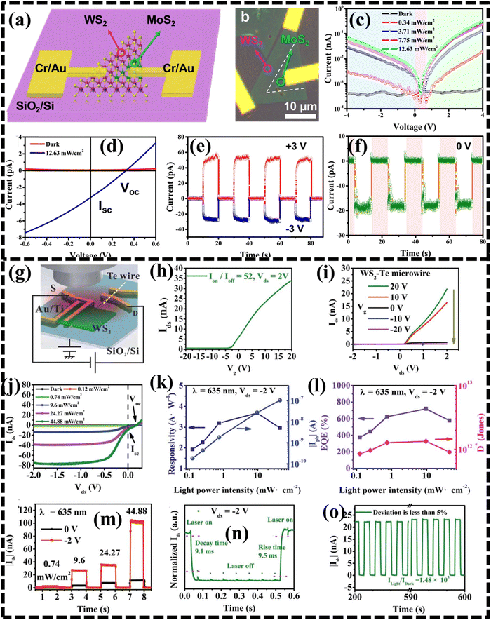 |
| | Fig. 14 (a) Schematic diagram of the heterostructures of MoS2 and WS2, (b) optical image of the device, (c) logarithmic I–V characteristics of the device under different illumination intensities, (d) the magnified I–V characteristics near 0 V of applied bias, (e) I–t characteristics for on–off switching and (f) self-powered photovoltaic mode at 0 V of applied bias potential. Reprinted with permission from ref. 158, Copyright of Elsevier 2018. (g) Schematic diagram of the heterostructure photodetector device, (h) the transfer curve of the device, (i) output characteristics of the device, (j) I–V characteristics under dark and illumination conditions, (k) photoresponsivity and the net photocurrent as a function of illumination intensity, (l) EQE and detectivity of the device, (m) time dependent photocurrent of the device, (n) time dependent photo response of the device and (o) stability of the photodetector device over 200 cycles. Reprinted with permission from ref. 159, Copyright of Royal Society Chemistry 2021. | |
6.3. Metal–semiconductor–metal (MSM) and Schottky photodetectors
A photodetector known as a metal–semiconductor–metal (MSM) photodetector detects light using a metal–semiconductor–metal construction. A transition metal dichalcogenide, for example, often makes up the semiconductor layer in an MSM photodetector based on 2D materials (TMDC). The two metal layers, one on top and one at the bottom of the 2D material serve as electrodes to measure the photocurrent produced by light absorption. The Schottky contact between the semiconductor and the metal in an MSM photodetector creates an internal electric field that separates electron–hole pairs created by light absorption in the semiconductor layer. The schematic device construction of the photodetector with the MoS2 active layer and Ti/Au electrodes is shown in Fig. 15(a), whereas Fig. 15(b) displays the I–V characteristics measured in the voltage range of −5 to +5 V.160Fig. 15(c) shows the responsivity of this device with different light intensities and Fig. 15(d) exhibits the responsivity with respect to applied bias at different illumination intensities. A current that can be measured as an output signal is produced as a result of the movement of electrons and holes. The advantages of MSM photodetectors based on 2D materials are high sensitivity, high responsivity, and quick response times. Moreover, the high electron mobility of the device and robust light–matter interactions, which can improve its performance as a photodetector, are made possible by the use of 2D TMDCs as the semiconductor layers.161 The need for high-quality metal-semiconductor interfaces, as well as the need to design the device structure and the doping levels to achieve good performance, are some of the limits of MSM photodetectors based on 2D materials. Spectroscopy, imaging, and sensing are just a few of the many applications that MSM photodetectors based on 2D materials are utilized in. They are also frequently utilized in the detection of electromagnetic radiation in the ultraviolet, visible, and infrared spectra as well as light-sensitive components in optical communication systems, such as fiber-optic networks. Moreover, a new generation of photomultipliers, which are extremely sensitive light detectors, has been developed using these technologies. MSM (metal–semiconductor–metal) based TMDC photodetectors are a class of photodetectors that use TMDCs as the active component. These photodetectors have a wide bandgap, high carrier mobility, and a high absorption coefficient, which provide them several benefits over conventional silicon-based photodetectors. The ability to detect light with extremely high sensitivity is one of the key benefits of TMDC-based MSM photodetectors. They are suitable for high-speed optical communication applications because of their quick response times, which are on the order of picoseconds. The ability to function at extremely low light levels, which makes them suited for low-light imaging applications, is another benefit of TMDC-based MSM photodetectors. The range of applications for these devices is also increased by the fact that they can function at a broad range of wavelengths, including in the ultraviolet and infrared sections of the spectrum. The need for high-quality TMDC materials and the necessity of adequate device construction and encapsulation to reduce environmental degradation are some of the difficulties faced by TMDC-based MSM photodetectors. Overall, TMDC-based MSM photodetectors are a promising technology with many potential uses, but more study and development are required to properly tap into their potential. Table 4 summarizes some functionalized TMDC MSM photodetectors with their important parameters. The absorption of light by the TMDC material, which results in the formation of electron–hole pairs, is the basis for the operation of TMDC-based MSM photodetectors. The internal electric field of the device then divides these electron–hole pairs, with the electrons going to the n-type contact and the holes to the p-type contact.162 As a result, the device generates a current flow that may be monitored to find the existence of light. The TMDC material is commonly sandwiched between two metal contacts in MSM photodetectors based on TMDCs, thus the term “metal–semiconductor–metal” (MSM). In addition to acting as the device's electrical contacts, the metal contacts also combine with the TMDC material to form a Schottky barrier that aids in separating the electron–hole pairs and boosts the effectiveness. With TMDC-based MSM photodetectors, light can be absorbed through various methods, such as excitonic absorption, indirect inter-band transition, and direct inter-band transition. Depending on the type of TMDC materials utilized and the light wavelength being absorbed, a certain mechanism will occur. TMDC-based MSM photodetectors are renowned for their quick response times, which are on the order of picoseconds due to the high carrier mobility in TMDC materials, in addition to the aforementioned mechanism. The general operating principle of TMDC-based MSM photodetectors is based on the light absorption by the TMDC material, which generates electron–hole pairs, and the separation of these charges by the integrated electric field, which yields a current flow that can be measured to detect the presence of light.163 The signal produced by a photodetector, which in the case of TMDC-based MSM photodetectors is a current flow arising from the absorption of light, is amplified using the photomultiplication process. By increasing the signal-to-noise ratio of the detector, photomultiplication aims to make it more sensitive and capable of detecting weaker signals.164 The employment of a cascade of amplifiers, each of which amplifies the signal before it is sent on to the next stage, is one method of achieving photomultiplication in TMDC-based MSM photodetectors. Trans-impedance amplification, the name given to this sort of photomultiplication, is achieved by cascading several trans-impedance amplifiers (TIAs). Using an approach known as “avalanche photodetection,” which accelerates the electron–hole pairs created by the absorption of light to crash with other atoms and produce additional electron–hole pairs, is another method for achieving photomultiplication in TMDC-based MSM photodetectors. Impact ionization has the capacity to increase the number of charge carriers and, consequently, the current flow, producing a stronger signal. Remember that to prevent noise and saturation, both procedures would need to be carefully planned. It is important to note that MSM photodetectors based on TMDCs have demonstrated great responsiveness and quick response times, making them appropriate for low-light imaging applications and high-speed optical communication applications even without the usage of photomultiplication. In some circumstances, photomultiplication is another method that can be utilized to boost the sensitivity of the detector.
 |
| | Fig. 15 (a) Lateral device schematic structure of the photodetector, (b) I–V characteristics measured in the voltage range of the photodetector, (c) responsivity of the device with different light intensities and (d) responsivity with respect to applied bias at different illumination intensities. Reprinted with permission of ref. 160, Copyright of Nature 2016. | |
Table 4 Summary of the literature data for photodetectors based on two-dimensional transition metal dichalcogenides. The table contains some benchmark parameters (responsivity, EQE, and detectivity)
| Materials |
Device type |
Bias/incident light (V μW−1 cm−2) |
Responsivity (A W−1) |
Detectivity (Jones) |
EQE (%) |
Ref. |
| WSe2/PANI |
MSM |
15/1.0 × 104 |
0.056 |
5.8 × 10⁹ |
— |
165
|
| GeSe/MoS2 |
Diode |
0/3080 |
0.105 |
1.46 × 10¹⁰ |
24.2 |
166
|
| WS2/Alx/Ge |
Diode |
0/42 |
0.634 |
4.3 × 10¹¹ |
50 |
167
|
| WS2/Si |
Diode |
0/16.5 |
0.290 |
2.6 × 10¹⁴ |
— |
168
|
| WS2/GaAs |
Diode |
4/1.7 × 10−2 |
0.527 |
1.03 × 10¹⁴ |
— |
169
|
| WS2/Gr |
MSM |
—/10 |
8.050 |
2.8 × 10¹⁰ |
1.8 × 10³ |
170
|
| Si/SiO2/WS2 |
Diode |
0/0.27 |
2.31 |
9.16 × 10¹¹ |
22 |
171
|
| p-WSe2/n-Si |
Diode |
0/— |
0.67 |
1.59 × 10¹³ |
85 |
172
|
| SWCNT/MoS2 |
MSM |
1/10 |
2.01 × 10³ |
3.2 × 10¹² |
— |
173
|
| Bi2O2Se/MoTe2 |
Diode |
60/— |
4.96 |
3.84 × 10¹² |
7.21 |
174
|
| MoS2(1−x)Se2x |
Phototransistor |
0/1.73 × 105 |
0.311 |
1011 |
— |
175
|
| n-WS2/Si |
Diode |
−1/— |
0.87 |
1.8 × 10¹¹ |
161 |
176
|
| ZnO-WS2/Si |
Diode |
−2/200 |
9.48 |
1012 |
1758 |
177
|
| WSe2/Si |
Diode |
— |
1.15 |
1011 |
134 |
178
|
| WSe2/MoS2 |
Phototransistor |
20/5 × 10−3 |
2700 |
5 × 10¹¹ |
— |
179
|
| WS2/Polycrylamide |
MSM |
—/50 |
1.3742 |
1.52 × 10¹² |
465.93 |
52
|
| Au-MoS2/Si |
MSM |
—/792 |
0.128 |
1.32 × 10¹⁰ |
∼1.2 × 10⁸ |
180
|
| WS2 |
MSM |
— |
1093.1 |
2.6 × 10¹² |
2.1 × 10⁵ |
181
|
| MoS2/i-Ge |
MSM |
— |
0.7 |
— |
56.1 |
182
|
| WS2/AlOx/Ge |
MSM |
—/42 |
0.634 |
4.3 × 10¹¹ |
50.8 |
167
|
| Graphene/WS2/Ge |
MSM |
0/0.86 × 105 |
7.55 |
3 × 10¹² |
— |
183
|
| MoS2-Gr-MoS2 |
Phototransistor |
0.5/— |
0.030 |
109 |
— |
184
|
| ZnO/WSe2 |
Phototransistor |
— |
0.541 |
4.23 × 10⁹ |
— |
185
|
| ReS2 |
Phototransistor |
—/0.47 |
106 |
1013 |
— |
186
|
| GaTe |
Phototransistor |
5/0.29 × 103 |
274.3 |
1012 |
— |
187
|
| Te/WS2 |
Phototransistor |
0/— |
0.033 |
1.57 × 10⁶ |
— |
188
|
| MoS2 |
Phototransistor |
0/— |
104 |
1013 |
— |
189
|
The performance of a self-powered photodetector depends on various parameters, including responsivity, detectivity, NEP, on–off ratio, LDR, EQE etc. These parameters are influenced by the properties of materials used. The photodetector's operation is based on three distinct stages: light harvesting, separation of photocarriers, and the subsequent transport of charges. The light absorption capacity significantly impacts the performance of optoelectronic devices. To attain optimal results, light capture technology has been developed to extend the effective path length of light propagation and enhance the efficiency of photon collection.190 Following photon absorption, the generation of charge carriers is crucial, and the superior separation and collection of these carriers contribute to the improved performance of the photodetector. TMDCs may be doped to become either n-type (electron-donor) or p-type (hole-donor) by carefully adding certain impurities or foreign atoms. This will change their carrier concentration and produce an inherent potential. Because of its intrinsic potential, the photodetector can produce electricity on its own when light strikes it, making it a self-sufficient gadget that does not require an external power source.112 By changing their surface properties, such as WSe2 or MoS2, TMDCs can perform better in self-powered photodetection applications. Surface functionalization can be utilized to attach certain molecules or ligands, which will improve the TMDCs’ interaction with incident light and boost their photoresponsivity and capacity to absorb light.191 In photodetection applications, covalent functionalization offers a stable and long-lasting alteration of the TMDC surface, guaranteeing long-term performance and dependability. Tobias Scharl et al. investigated WS2 through exfoliation and combined it with perylene diamides (C36H29NO), which absorb visible light and accept electrons, creating adaptable electron-donor acceptor hybrids.192 Following the discovery of graphene, a variety of TMDCs have surfaced, showcasing remarkable performance utilized in photodetectors. However, despite their potential, TMDCs based photodetectors encounter numerous challenges. To achieve high performance and superior photodetectors, several approaches can be pursued: refining the preparation techniques for TMDCs to yield high quality outputs, and designing and optimizing antenna structures to align with detected wavelengths, thereby enhancing the photodetector sensitivity.
The significant possibility of TMDCs to transform the next generation of photodetectors, image sensors, optical transceivers, spectrometers, etc., depends on the successful development of initial prototypes. The awareness of this potential depends on advancing both technology and manufacturing willingness levels, achieved through concerted efforts between researchers, semiconductor foundries, and key industrial companies. The introduction of novel materials, such as TMDCs, holds the promise of enhancing the efficiency of self-powered photodetectors through the improvement of the open circuit voltage. Sustained investigation of creative nanostructures that facilitate effective separation of photogenerated electron hole pairs through simple and reliable fabrication methods remains a fundamental avenue for future research. With the introduction of high-performance semiconductor materials like TMDCs, there exists a significant opportunity to elevate performance of self-powered photodetectors by advancing both material design and device testing methodologies. Inspired by the popularity of wearable photodetectors in recent years, the next generation of photodetectors must be manufactured to represent greater adaptability and with improved intelligence. This naturally involves new criteria for the design, dimensions, and efficacy of both materials and structures.
7. Conclusions
With an emphasis on the potential of TMDCs to satisfy the market for high-performance photodetector devices, this analysis concludes with a thorough summary of the current status of self-powered photodetectors. Setting a systematic and beautiful scene, the introduction emphasized the significance of self-powered photodetectors in a range of applications and the ongoing research and innovation required in this area. The difficulties encountered by scientists in creating TMDC-based autonomous photodetectors were carefully investigated. These problems range from the synthesis and characterization of materials to the engineering and optimization of devices, underscoring the need for innovative and practical solutions in the years to come. The intrinsic qualities of TMDCs, which make them attractive options for self-powered photodetectors, were thoroughly examined in this study. High carrier mobilities, mechanical flexibility, thermal conductivity, strong spin-valley coupling, and advantageous optical and electronic properties are just a few of these attributes, which together highlight TMDCs' potential to meet the stringent requirements for self-powered photodetector applications. Furthermore, different functionalization strategies were covered in detail, including surface, covalent, and non-covalent functionalization, as well as avenues like doping, strain engineering, and photoinduced charge transfer for modulating optoelectronic properties. Taken together, these tactics offer a path forward for improving the efficiency of TMDC-based photodetectors. The use of TMDCs in self-powered photodetectors has great promise, and continued study and development in this area should result in ground-breaking discoveries that have an influence on a broad variety of applications, including communications, healthcare, and other fields. Exciting opportunities exist for the creation and application of effective, environmentally friendly, and multipurpose photodetector devices in the future. Currently, enhancing information exchange between humans and technology is crucial, particularly in fields such as communication, healthcare, and environmental monitoring. The demand for improved electronic products has grown, emphasizing the necessity for self-powered devices with straightforward structures; these devices offer practical advantages, including minimal maintenance requirements, low or no external power, wireless functionality, self-sustainability, and a prolonged lifespan, aiming to reduce complications and dependencies. The absorption of weak optical signals is delayed by the photogenerated carriers, necessitating an additional mechanism to enhance both the depletion region width and the electric field at the P–N junction within the self-powered photodetector. Consequently, addressing these challenges in self-powered photodetectors involves TMDCs under investigation.
Author contributions
Alka Rani: investigation and writing – original draft, Arpit Verma: investigation, review, and editing, and B. C. Yadav: validation and supervision.
Conflicts of interest
The authors declare that they have no known competing financial interest or personal relationships that could have appeared to influence the work reported in this paper.
Acknowledgements
Ms Alka Rani is thankful to the Council of Scientific & Industrial Research and University Grant Commission (CSIR-UGC), Government of India for financial support in the form of Junior Research Fellowship (NTA Ref. No.: 231610026817).
References
- W. Ahmad, J. Wu, Q. Zhuang, A. Neogi and Z. Wang, Small, 2023, 19, 2207641 CrossRef CAS PubMed.
- F. H. L. Koppens, T. Mueller, P. Avouris, A. C. Ferrari, M. S. Vitiello and M. Polini, Nat. Nanotechnol., 2014, 9, 780–793 CrossRef CAS PubMed.
- A. Verma, P. Chaudhary, R. K. Tripathi and B. C. Yadav, Sustainable Energy Fuels, 2021, 5, 1394–1405 RSC.
- X. Bao, Q. Ou, Z. Q. Xu, Y. Zhang, Q. Bao and H. J. A. M. T. Zhang, Adv. Mater. Technol., 2018, 3, 1800072 CrossRef.
- K. Kalantar-zadeh, J. Z. Ou, T. Daeneke, M. S. Strano, M. Pumera and S. L. Gras, Adv. Funct. Mater., 2015, 25, 5086–5099 CrossRef CAS.
- J. Ping, Z. Fan, M. Sindoro, Y. Ying and H. Zhang, Adv. Funct. Mater., 2017, 27, 1605817 CrossRef.
- Q. Liang, Q. Zhang, X. Zhao, M. Liu and A. T. S. Wee, ACS Nano, 2021, 15, 2165–2181 CrossRef CAS PubMed.
- M. Chhowalla, H. S. Shin, G. Eda, L.-J. Li, K. P. Loh and H. J. Zhang, Nat. Chem., 2013, 5, 263–275 CrossRef PubMed.
- L. Dou, Y. Yang, J. You, Z. Hong, W.-H. Chang, G. Li and Y. Yang, Nat. Commun., 2014, 5, 5404 CrossRef CAS PubMed.
- C. X. Li, C. Chen, L. Zhao and N. Ma, ACS Appl. Mater. Interfaces, 2023, 15, 23402–23411 CrossRef CAS PubMed.
- X. Xue, C. Ling, H. Ji, J. Wang, C. Wang, H. Lu and W. Liu, ACS Appl. Mater. Interfaces, 2023, 15, 5411–5419 CrossRef CAS PubMed.
- C. K. Zankat, P. M. Pataniya, A. Patel, S. A. Bhakhar, S. Narayan, G. K. Solanki, K. D. Patel, V. M. Pathak, C. K. Sumesh and P. K. Jha, Mater. Today Energy, 2020, 18, 100550 CrossRef CAS.
- J. Zhong, X. Zhang and G. Xiang, ACS Appl. Mater. Interfaces, 2023, 15, 35753–35787 CrossRef PubMed.
- M. Sun, P. Yang, D. Xie, Y. Sun, J. Xu, T. Ren and Y. Zhang, Adv. Electron. Mater., 2019, 5, 1800580 CrossRef.
- L. H. Zeng, S. H. Lin, Z. J. Li, Z. X. Zhang, T. F. Zhang, C. Xie, C. H. Mak, Y. Chai, S. P. Lau and L. B. Luo, Adv. Funct. Mater., 2018, 28, 1705970 CrossRef.
- K. Murali and K. Majumdar, IEEE Trans. Electron Devices, 2018, 65, 4141–4148 CAS.
- D. B. Velusamy, R. H. Kim, S. Cha, J. Huh, R. Khazaeinezhad, S. H. Kassani, G. Song, S. M. Cho, S. H. Cho and I. Hwang, Nat. Commun., 2015, 6, 8063 CrossRef PubMed.
- C. B. Vining, J. Appl. Phys., 1991, 69, 331–341 CrossRef CAS.
- S. Manzeli, D. Ovchinnikov, D. Pasquier, O. V. Yazyev and A. Kis, Nat. Rev. Mater., 2017, 2, 1–15 Search PubMed.
- S. H. Mir, V. K. Yadav and J. K. Singh, ACS Omega, 2020, 5, 14203–14211 CrossRef CAS PubMed.
- F. Yan, Z. Wei, X. Wei, Q. Lv, W. Zhu and K. Wang, Small Methods, 2018, 2, 1700349 CrossRef.
- W. Choi, N. Choudhary, G. H. Han, J. Park, D. Akinwande and Y. H. Lee, Mater. Today, 2017, 20, 116–130 CrossRef CAS.
- Y. Fang, Y. Ge, C. Wang and H. Zhang, Laser Photonics Rev., 2020, 14, 1900098 CrossRef CAS.
- Z. Huang, W. Zhang and W. J. Zhang, Materials, 2016, 9, 716 CrossRef PubMed.
- Z. Ye, T. Cao, K. O’brien, H. Zhu, X. Yin, Y. Wang, S. G. Louie and X. Zhang, J. Nat., 2014, 513, 214–218 CrossRef CAS PubMed.
- W. Choi, J. Ahn, K. T. Kim, H. J. Jin, S. Hong, D. K. Hwang and S. Im, Adv. Mater., 2021, 33, 2103079 CrossRef CAS PubMed.
- L. Huang, A. Krasnok, A. Alú, Y. Yu, D. Neshev and A. E. Miroshnichenko, Rep. Prog. Phys., 2022, 85, 046401 CrossRef PubMed.
- A. Verma and B. C. Yadav, ACS Appl. Nano Mater., 2023, 6, 5493–5507 CrossRef CAS.
- M. Bernardi, M. Palummo and J. C. J. Grossman, Nano Lett., 2013, 13, 3664–3670 CrossRef CAS PubMed.
- O. Lopez-Sanchez, D. Lembke, M. Kayci, A. Radenovic and A. J. Kis, Nat. Nanotechnol., 2013, 8, 497–501 CrossRef CAS PubMed.
- J. Cheng, C. Wang, X. Zou and L. J. Liao, Adv. Opt. Mater., 2019, 7, 1800441 CrossRef.
- A. Autere, H. Jussila, Y. Dai, Y. Wang, H. Lipsanen and Z. Sun, Adv. Mater., 2018, 30, 1705963 CrossRef PubMed.
- A. Manikandan, Y.-Z. Chen, C.-C. Shen, C.-W. Sher, H.-C. Kuo and Y.-L. Chueh, Prog. Quantum Electron., 2019, 68, 100226 CrossRef.
- W. Yu, S. Li, Y. Zhang, W. Ma, T. Sun, J. Yuan, K. Fu and Q. Bao, J. Small, 2017, 13, 1700268 CrossRef PubMed.
- P. Pataniya, C. K. Zankat, M. Tannarana, C. K. Sumesh, S. Narayan, G. K. Solanki, K. D. Patel, V. M. Pathak and P. K. Jha, ACS Appl. Nano Mater., 2019, 2, 2758–2766 CrossRef CAS.
-
H. Kumar and S. Jit, Handbook of II-VI Semiconductor-Based Sensors and Radiation Detectors: Volume 2, Photodetectors, Springer, 2023, pp. 495–515 Search PubMed.
- S. Ahmed and J. Yi, Nano-Micro Lett., 2017, 9, 1–23 CrossRef PubMed.
- C. Mu, J. Xiang and Z. Liu, J. Mater. Res., 2017, 32, 4115–4131 CrossRef CAS.
- A. Singh, A. Verma, B. C. Yadav and P. Chauhan, Dalton Trans., 2022, 51, 7864–7877 RSC.
- A. Verma, P. Chaudhary, R. K. Tripathi, A. Singh and B. C. Yadav, J. Inorg. Organomet. Polym. Mater., 2022, 32, 2807–2826 CrossRef CAS.
- T. Ouyang, X. Zhao, X. Xun, F. Gao, B. Zhao, S. Bi, Q. Li, Q. Liao and Y. Zhang, Adv. Sci., 2023, 2301585 CrossRef CAS PubMed.
- M. Reddeppa, S. B. Mitta, T. Chandrakalavathi, B.-G. Park, G. Murali, R. Jeyalakshmi, S.-G. Kim, S. H. Park and M.-D. Kim, Curr. Appl. Phys., 2019, 19, 938–945 CrossRef.
- R. Raj, P. Lohia, D. Dwivedi, A. Verma and B. C. Yadav, J. Mater. Sci.: Mater. Electron., 2022, 33, 17939–17948 CrossRef CAS.
- R. Chai, Z. Lou and G. Shen, J. Mater. Chem. C, 2019, 7, 4581–4586 RSC.
- M. Kumar, J. Lim, H. Kang, S. Kim and H. Seo, Nano Energy, 2021, 82, 105668 CrossRef CAS.
- W. Tian, Y. Wang, L. Chen and L. Li, Small, 2017, 13, 1701848 CrossRef PubMed.
- T. Lulé, S. Benthien, H. Keller, F. A. M. F. Mutze, P. Rieve, K. Seibel, M. Sommer and M. A. B. M. Bohm, IEEE Trans. Electron Devices, 2000, 47, 2110–2122 CrossRef.
- L. Su, W. Yang, J. Cai, H. Chen and X. Fang, Small, 2017, 13, 1701687 CrossRef PubMed.
- M. Gao, L. Yu, Q. Lv, F. Kang, Z.-H. Huang and R. Lv, J. Materiomics, 2023, 9, 768–786 CrossRef.
- K. Han, G. Huang, Y. Jia, Q. Niu, Z. Zheng and B. Wang, Opt. Mater., 2024, 148, 114971 CrossRef CAS.
- S. Maity, K. Sarkar and P. Kumar, J. Mater. Chem. C, 2021, 9, 14532–14572 RSC.
- A. Verma, P. Chaudhary, R. K. Tripathi and B. C. Yadav, Mater. Adv., 2022, 3, 3994–4005 RSC.
-
P. Stallinga, Electrical characterization of organic electronic materials and devices, John Wiley & Sons, 2009 Search PubMed.
- F. Giubileo and A. Di Bartolomeo, Prog. Surf. Sci., 2017, 92, 143–175 CrossRef CAS.
- J. Wang, Q. Yao, C. W. Huang, X. Zou, L. Liao, S. Chen, Z. Fan, K. Zhang, W. Wu and X. Xiao, Adv. Mater., 2016, 28, 8302–8308 CrossRef CAS PubMed.
- M. Kim, K. Y. Ma, H. Kim, Y. Lee, J. H. Park and H. S. Shin, Adv. Mater., 2022, 2205520 Search PubMed.
- A. Sebastian, R. Pendurthi, T. H. Choudhury, J. M. Redwing and S. Das, Nat. Commun., 2021, 12, 693 CrossRef CAS PubMed.
- N. A. Jayah, H. Yahaya, M. R. Mahmood, T. Terasako, K. Yasui and A. M. Hashim, Nanoscale Res. Lett., 2015, 10, 1–10 CrossRef CAS PubMed.
-
R. K. Willardson and A. C. Beer, Semiconductors and semimetals, Academic Press, 1977 Search PubMed.
- N. Ma, N. Tanen, A. Verma, Z. Guo, T. Luo, H. G. Xing and D. Jena, Appl. Phys. Lett., 2016, 109, 212101 CrossRef.
- P. Bagheri, C. Quiñones-Garcia, D. Khachariya, S. Rathkanthiwar, P. Reddy, R. Kirste, S. Mita, J. Tweedie, R. Collazo and Z. Sitar, J. Appl. Phys., 2022, 132, 185703 CrossRef CAS.
- C. G. Rodrigues, Microelectron. J., 2006, 37, 657–660 CrossRef CAS.
- M. Nathan, W. Dumke, K. Wrenner, S. Tiwari, S. Wright and K. Jenkins, Appl. Phys. Lett., 1988, 52, 654–656 CrossRef CAS.
- S. Kim, A. Konar, W.-S. Hwang, J. H. Lee, J. Lee, J. Yang, C. Jung, H. Kim, J.-B. Yoo and J.-Y. Choi, Nat. Commun., 2012, 3, 1011 CrossRef PubMed.
- H. Wang, C. H. Chan, C. H. Suen, S. P. Lau and J.-Y. Dai, ACS Nano, 2019, 13, 6008–6016 CrossRef CAS PubMed.
- X.-Y. Gao, J.-M. Zhang, A. Ali, X.-M. Wei and Y.-H. Huang, Thin Solid Films, 2021, 732, 138790 CrossRef CAS.
- M. Hamada, K. Matsuura, T. Sakamoto, I. Muneta, T. Hoshii, K. Kakushima, K. Tsutsui and H. Wakabayashi, IEEE J. Electron Devices Soc., 2019, 7, 1258–1263 CAS.
- T. Kanazawa, T. Amemiya, A. Ishikawa, V. Upadhyaya, K. Tsuruta, T. Tanaka and Y. Miyamoto, Sci. Rep., 2016, 6, 22277 CrossRef CAS PubMed.
- I. Setiyawati, K.-R. Chiang, H.-M. Ho and Y.-H. Tang, Chin. J. Phys., 2019, 62, 151–160 CrossRef CAS.
- Y. Ma, A. Kuc, Y. Jing, P. Philipsen and T. Heine, Angew. Chem., Int. Ed., 2017, 56, 10214–10218 CrossRef CAS PubMed.
- H. Chen, Z. Li, L. Guo and X. Chen, Europhys. Lett., 2017, 117, 27009 CrossRef.
- H. C. Movva, A. Rai, S. Kang, K. Kim, B. Fallahazad, T. Taniguchi, K. Watanabe, E. Tutuc and S. K. Banerjee, ACS Nano, 2015, 9, 10402–10410 CrossRef CAS PubMed.
- T. Li, Z. Zhang, W. Zheng, Y. Lv and F. Huang, AIP Adv., 2016, 6, 115207 CrossRef.
- Y. Wang, T. Sohier, K. Watanabe, T. Taniguchi, M. J. Verstraete and E. Tutuc, Appl. Phys. Lett., 2021, 118, 102105 CrossRef CAS.
- C. Xie and F. Yan, Small, 2017, 13, 1701822 CrossRef PubMed.
- P. Wang, Y. Lan, C. Huan, J. Luo, W. Cai, J. Fan, X. He, Z. Huang, L. Zhu and Q. Ke, Mater. Sci. Eng., R, 2023, 156, 100759 CrossRef.
- P. Chauhan, A. B. Patel, G. K. Solanki, H. K. Machhi, S. S. Soni, V. M. Pathak, V. Patel, S. Narayan and P. K. Jha, Adv. Opt. Mater., 2021, 9, 2100993 CrossRef CAS.
- A. Verma, A. Singh, P. Chaudhary, R. K. Tripathi, B. C. Yadav, P. Chauhan and D. Kumar, Mater. Adv., 2023, 4, 1062–1074 RSC.
- H. Wang, H. Yuan, S. S. Hong, Y. Li and Y. Cui, Chem. Soc. Rev., 2015, 44, 2664–2680 RSC.
- M. Tebyetekerwa, J. Zhang, Z. Xu, T. N. Truong, Z. Yin, Y. Lu, S. Ramakrishna, D. Macdonald and H. T. Nguyen, ACS Nano, 2020, 14, 14579–14604 CrossRef CAS PubMed.
- A. Michail, J. Parthenios, D. Anestopoulos, C. Galiotis, M. Christian, L. Ortolani, V. Morandi and K. Papagelis, 2D Mater., 2018, 5, 035035 CrossRef.
- Y. Zou, Z. Zhang, J. Yan, L. Lin, G. Huang, Y. Tan, Z. You and P. Li, Nat. Commun., 2022, 13, 4372 CrossRef CAS PubMed.
- L. Peng, Y. Zhu, H. Li and G. Yu, Small, 2016, 12, 6183–6199 CrossRef CAS PubMed.
- L. Lv, H. Ai, T. Chen, W. Zhu, Y. Guo, L. Dong and S. Song, J. Mater. Chem. A, 2023, 11, 7115–7127 RSC.
- B. Wang, Y. Yan, B. Qin, Z. Ye, J. Cao and J. Qi, Chem. Eng. J., 2023, 476, 146535 CrossRef CAS.
- X. Gu and C. Y. Zhao, Comput. Mater. Sci., 2019, 165, 74–81 CrossRef CAS.
- M. H. Khan, H. K. Liu, X. Sun, Y. Yamauchi, Y. Bando, D. Golberg and Z. Huang, Mater. Today, 2017, 20, 611–628 CrossRef CAS.
- D. Akinwande, N. Petrone and J. Hone, Nat. Commun., 2014, 5, 5678 CrossRef CAS PubMed.
- G. Ding, G. Y. Gao, Z. Huang, W. Zhang and K. Yao, Nanotechnology, 2016, 27, 375703 CrossRef PubMed.
- A. Ansh, U. Patbhaje, J. Kumar, A. Meersha and M. Shrivastava, Commun. Mater., 2023, 4, 8 CrossRef CAS.
- W.-X. Zhou and K.-Q. Chen, Sci. Rep., 2015, 5, 15070 CrossRef CAS PubMed.
- X. Hu, L. Yan, L. Ding, N. Zheng, D. Li, T. Ji, N. Chen and J. Hu, Coord. Chem. Rev., 2024, 499, 215504 CrossRef CAS.
- C. S. Lau, S. Das, I. A. Verzhbitskiy, D. Huang, Y. Zhang, T. Talha-Dean, W. Fu, D. Venkatakrishnarao and K. E. Johnson Goh, ACS Nano, 2023, 17, 9870–9905 CrossRef CAS PubMed.
- Y. Zhang, J. van den Brink, C. Felser and B. Yan, 2D Mater., 2018, 5, 044001 CrossRef CAS.
- S. Yang, Y. Chen and C. Jiang, InfoMat, 2021, 3, 397–420 CrossRef.
- S. Chen, Y. Fu, M. Ishaq, C. Li, D. Ren, Z. Su, X. Qiao, P. Fan, G. Liang and J. Tang, InfoMat, 2023, e12400 CrossRef CAS.
- Z. Li, T. Yan and X. Fang, Nat. Rev. Mater., 2023, 8, 587–603 CrossRef.
- L. Liao, E. Kovalska, J. Regner, Q. Song and Z. Sofer, Small, 2023, 2303638 Search PubMed.
- M. van der Laan, E. Heemskerk, F. Kienhuis, N. Diepeveen, D. Poonia, S. Kinge, M. T. Dang, V. A. Dinh, L. D. A. Siebbeles and A. Isaeva, ACS Photonics, 2023, 10, 3115–3123 CrossRef CAS PubMed.
- M. R. Molas, K. Gołasa, Ł. Bala, K. Nogajewski, M. Bartos, M. Potemski and A. Babiński, Sci. Rep., 2019, 9, 1989 CrossRef PubMed.
- V. Iberi, L. Liang, A. V. Ievlev, M. G. Stanford, M.-W. Lin, X. Li, M. Mahjouri-Samani, S. Jesse, B. G. Sumpter, S. V. Kalinin, D. C. Joy, K. Xiao, A. Belianinov and O. S. Ovchinnikova, Sci. Rep., 2016, 6, 30481 CrossRef CAS PubMed.
- H.-L. Liu, T. Yang, J.-H. Chen, H.-W. Chen, H. Guo, R. Saito, M.-Y. Li and L.-J. Li, Sci. Rep., 2020, 10, 15282 CrossRef CAS PubMed.
- T. N. Lin, S. Santiago, S. P. Caigas, C. T. Yuan, T. Y. Lin, J. L. Shen and Y. F. Chen, npj 2D Mater. Appl., 2019, 3, 46 CrossRef.
- R. Dong and I. Kuljanishvili, J. Vac. Sci. Technol., B: Nanotechnol. Microelectron.: Mater., Process., Meas., Phenom., 2017, 35, 030803 Search PubMed.
- S. Sahare, P. Ghoderao, M. K. Sharma, M. Solovan, R. Aepuru, M. Kumar, Y. Chan, Z. Ziółek, S.-L. Lee and Z.-H. Lin, Nano Energy, 2023, 107, 108172 CrossRef CAS.
- I. Zulfiqar, M. A. Khan, S. Gul, N. U. L. Hassan, M. A. Rehman, M. A. Basit, H. W. Khalil, M. Ouladsmane, S. Rehman and M. F. Khan, Phys. B, 2023, 669, 415313 CrossRef CAS.
- C. Gautam, A. Verma, P. Chaudhary and B. C. Yadav, Opt. Mater., 2022, 123, 111860 CrossRef CAS.
- X.-G. Zhao, Z. Shi, X. Wang, H. Zou, Y. Fu and L. Zhang, InfoMat, 2021, 3, 201–211 CrossRef CAS.
- T. Kim, J. Lim, J. Byeon, Y. Cho, W. Kim, J. Hong, S. Jin Heo, J. Eun Jang, B.-S. Kim, J. Hong, S. Pak and S. Cha, Small Struct., 2023, 4, 2200274 CrossRef CAS.
- K. Novoselov, J. Sci., 2016, 353, 6298 Search PubMed.
- P. Zhao, D. Kiriya, A. Azcatl, C. Zhang, M. Tosun, Y.-S. Liu, M. Hettick, J. S. Kang, S. McDonnell and S. J. KC, ACS Nano, 2014, 8, 10808–10814 CrossRef CAS PubMed.
- S. Wang, D. Ding, P. Li, Y. Sui, G. Liu, S. Zhao, R. Xiao, C. Tian, Z. Chen and H. Wang, Small, 2023, 2301027 CrossRef CAS PubMed.
- S. Mubeen, T. Zhang, B. Yoo, M. A. Deshusses and N. V. Myung, J. Phys. Chem. C, 2007, 111, 6321–6327 CrossRef CAS.
- J. L. Johnson, A. Behnam, S. J. Pearton and A. Ural, Adv. Mater., 2010, 22, 4877–4880 CrossRef CAS PubMed.
- W. Hu, T. Wang, R. Zhang and J. Yang, J. Phys. Chem. C, 2016, 4, 1776–1781 CAS.
- Y. Yue, Y. Feng, J. Chen, D. Zhang and W. J. Feng, J. Mater. Chem. C, 2017, 5, 5887–5896 RSC.
- S. Li, S. Tian, Y. Yao, M. He, L. Chen, Y. Zhang and J. Zhai, Nanomaterials, 2021, 11, 769 CrossRef CAS PubMed.
- Y. Tao, S. W. Koh, X. Yu, C. Wang, H. Liang, Y. Zhang, H. Li and Q. J. Wang, Nanoscale Adv., 2019, 1, 4783–4789 RSC.
- R.-J. Chang, Y. Sheng, G. H. Ryu, N. Mkhize, T. Chen, Y. Lu, J. Chen, J. K. Lee, H. Bhaskaran and J. H. Warner, ACS Appl. Mater. Interfaces, 2019, 11, 24279–24288 CrossRef CAS PubMed.
- S. Li, J. Hong, B. Gao, Y. C. Lin, H. E. Lim, X. Lu, J. Wu, S. Liu, Y. Tateyama and Y. Sakuma, Adv. Sci., 2021, 8, 2004438 CrossRef CAS PubMed.
- D. Bhattacharya, S. Mukherjee, R. K. Mitra and S. K. Ray, Nanotechnology, 2023, 34, 435401 CrossRef PubMed.
-
K. Thakar and S. Lodha, 2D Materials for Electronics, Sensors and Devices, Elsevier, 2023, pp. 207–258 Search PubMed.
-
C. S. Rout, 2D Materials-Based Electrochemical Sensors, Elsevier, 2023 Search PubMed.
- H. Guo, N. Lu, L. Wang, X. Wu and X. C. Zeng, J. Phys. Chem. C, 2014, 118, 7242–7249 CrossRef CAS.
- P. Johari and V. B. J. A. n Shenoy, ACS Nano, 2012, 6, 5449–5456 CrossRef CAS PubMed.
- W. S. Yun, S. Han, S. C. Hong, I. G. Kim and J. J. Lee, Phys. Rev. B: Condens. Matter Mater. Phys., 2012, 85, 033305 CrossRef.
- Q. Yue, J. Kang, Z. Shao, X. Zhang, S. Chang, G. Wang, S. Qin and J. J. Li, Phys. Lett. A, 2012, 376, 1166–1170 CrossRef CAS.
- H. Guo, N. Lu, L. Wang, X. Wu and X. C. Zeng, J. Phys. Chem. C, 2014, 118, 7242–7249 CrossRef CAS.
- Y. Chen, W. Deng, X. Chen, Y. Wu, J. Shi, J. Zheng, F. Chu, B. Liu, B. An and C. You, Nano Res., 2021, 1–7 Search PubMed.
- J. Li, Z. Shan and E. Ma, MRS Bull., 2014, 39, 108–114 CrossRef CAS.
- J. Du, Q. Liao, M. Hong, B. Liu, X. Zhang, H. Yu, J. Xiao, L. Gao, F. Gao and Z. Kang, Nano Energy, 2019, 58, 85–93 CrossRef CAS.
- M. A. K. Purbayanto, M. Chandel, M. Birowska, A. Rosenkranz and A. M. Jastrzębska, Adv. Mater., 2023, 2301850 CrossRef CAS PubMed.
- S. Roy, Aastha, K. A. Deo, K. Dey, A. K. Gaharwar and A. Jaiswal, ACS Appl. Mater. Interfaces, 2023, 15, 35753–35787 CrossRef CAS PubMed.
- D. B. Sulas-Kern, E. M. Miller and J. L. Blackburn, Energy Environ. Sci., 2020, 13, 2684–2740 RSC.
- K. F. Mak, C. Lee, J. Hone, J. Shan and T. F. J. Heinz, Phys. Rev. Lett., 2010, 105, 136805 CrossRef PubMed.
- W. Zhao, Z. Ghorannevis, L. Chu, M. Toh, C. Kloc, P.-H. Tan and G. J. Eda, ACS Nano, 2013, 7, 791–797 CrossRef CAS PubMed.
- J. Choi, H. Zhang and J. H. J. Choi, ACS Nano, 2016, 10, 1671–1680 CrossRef CAS PubMed.
- S. Mouri, Y. Miyauchi and K. J. Matsuda, Nano Lett., 2013, 13, 5944–5948 CrossRef CAS PubMed.
- N. Peimyoo, W. Yang, J. Shang, X. Shen, Y. Wang and T. J. Yu, ACS Nano, 2014, 8, 11320–11329 CrossRef CAS PubMed.
- J. D. Lin, C. Han, F. Wang, R. Wang, D. Xiang, S. Qin, X.-A. Zhang, L. Wang, H. Zhang and A. T. S. J. Wee, ACS Nano, 2014, 8, 5323–5329 CrossRef CAS PubMed.
- M. Patel, P. M. Pataniya, D. J. Late and C. K. Sumesh, Appl. Surf. Sci., 2021, 538, 148121 CrossRef CAS.
- B. Chen, S. Sui, F. He, C. He, H.-M. Cheng, S.-Z. Qiao, W. Hu and N. Zhao, Chem. Soc. Rev., 2023, 7802–7847 RSC.
- B. Han, S. M. Gali, S. Dai, D. Beljonne and P. Samorì, ACS Nano, 2023, 17, 17956–17965 CrossRef CAS PubMed.
- D. O. Li, M. S. Gilliam, X. S. Chu, A. Yousaf, Y. Guo, A. A. Green and Q. H. Wang, Mol. Syst. Des. Eng., 2019, 4, 962–973 RSC.
- X. S. Chu, A. Yousaf, D. O. Li, A. A. Tang, A. Debnath, D. Ma, A. A. Green, E. J. Santos and Q. H. Wang, Chem. Mater., 2018, 30, 2112–2128 CrossRef CAS.
- X. Liu, Y. Niu, D. Jin, J. Zeng, W. Li, L. Wang, Z. Hou, Y. Feng, H. Li and H. Yang, J. Colloid Interface Sci., 2023, 649, 909–917 CrossRef CAS PubMed.
- A. S. Siddiqui, A. Hayat, L. A. G. Pohan, M. A. Ahmad and M. Nasir, Mater. Today Chem., 2023, 32, 101625 CrossRef CAS.
- N. V. Kozhemyakina, J. M. Englert, G. Yang, E. Spiecker, C. D. Schmidt, F. Hauke and A. Hirsch, Adv. Mater., 2010, 22, 5483–5487 CrossRef CAS PubMed.
- A. J. Molina-Mendoza, L. Vaquero-Garzon, S. Leret, L. de Juan-Fernández, E. M. Pérez and A. Castellanos-Gomez, Chem. Commun., 2016, 52, 14365–14368 RSC.
- E. P. Nguyen, B. J. Carey, C. J. Harrison, P. Atkin, K. J. Berean, E. Della Gaspera, J. Z. Ou, R. B. Kaner, K. Kalantar-Zadeh and T. Daeneke, Nanoscale Adv., 2016, 8, 16276–16283 RSC.
- M. C. Rodríguez González, R. Sasikumar and S. De Feyter, Surf. Rev. Lett., 2021, 28, 2140002 CrossRef.
- Y. Zhao, S. Ippolito and P. Samori, Adv. Opt. Mater., 2019, 7, 1900286 CrossRef.
- G. R. Bhimanapati, Z. Lin, V. Meunier, Y. Jung, J. Cha, S. Das, D. Xiao, Y. Son, M. S. Strano and V. R. Cooper, ACS Nano, 2015, 9, 11509–11539 CrossRef CAS PubMed.
- K. Shi, J. Li, Y. Xiao, L. Guo, X. Chu, Y. Zhai, B. Zhang, D. Lu and F. Rosei, ACS Appl. Mater. Interfaces, 2020, 12, 31382–31391 CrossRef CAS PubMed.
- R. Nur, T. Tsuchiya, K. Toprasertpong, K. Terabe, S. Takagi and M. Takenaka, Commun. Mater., 2020, 1, 103 CrossRef.
-
F. F. Masouleh and N. Das, Application of Metal-Semiconductor-Metal Photodetector in High-Speed Optical Communication Systems, in Advances in Optical Communication, ed. N. Das, 2014 DOI:10.5772/58997.
- W. Zhi, Q. Quan, P. Yu and Y. Jiang, Micromachines, 2020, 11, 65 CrossRef PubMed.
- W. Wu, Q. Zhang, X. Zhou, L. Li, J. Su, F. Wang and T. Zhai, Nano Energy, 2018, 51, 45–53 CrossRef CAS.
- L. Han, M. Yang, P. Wen, W. Gao, N. Huo and J. Li, Nanoscale Adv., 2021, 3, 2657–2665 RSC.
- L. Zeng, L. Tao, C. Tang, B. Zhou, H. Long, Y. Chai, S. P. Lau and Y. H. Tsang, Sci. Rep., 2016, 6, 20343 CrossRef CAS PubMed.
- Q. Qiu and Z. Huang, Adv. Mater., 2021, 33, 2008126 CrossRef CAS PubMed.
- H. K. Sandhu, J. W. John, A. Jakhar, A. Sharma, A. Jain and S. Das, Adv. Mater. Interfaces, 2022, 9, 2102200 CrossRef CAS.
- C. Xie, C. Mak, X. Tao and F. Yan, Adv. Funct. Mater., 2017, 27, 1603886 CrossRef.
- J. Kublitski, A. Fischer, S. Xing, L. Baisinger, E. Bittrich, D. Spoltore, J. Benduhn, K. Vandewal and K. Leo, Nat. Commun., 2021, 12, 4259 CrossRef CAS PubMed.
- D. Kannichankandy, P. M. Pataniya, C. K. Zankat, M. Tannarana, V. M. Pathak, G. K. Solanki and K. D. Patel, Appl. Surf. Sci., 2020, 524, 146589 CrossRef CAS.
- Y. Xin, X. Wang, Z. Chen, D. Weller, Y. Wang, L. Shi, X. Ma, C. Ding, W. Li and S. Guo, ACS Appl. Mater. Interfaces, 2020, 12, 15406–15413 CrossRef CAS PubMed.
- D. Wu, J. Guo, C. Wang, X. Ren, Y. Chen, P. Lin, L. Zeng, Z. Shi, X. J. Li and C.-X. Shan, ACS Nano, 2021, 15, 10119–10129 CrossRef CAS PubMed.
- D. Wu, C. Guo, Z. Wang, X. Ren, Y. Tian, Z. Shi, P. Lin, Y. Tian, Y. Chen and X. Li, Nanoscale, 2021, 13, 13550–13557 RSC.
- C. Jia, X. Huang, D. Wu, Y. Tian, J. Guo, Z. Zhao, Z. Shi, Y. Tian, J. Jie and X. Li, Nanoscale, 2020, 12, 4435–4444 RSC.
- M. Alamri, M. Gong, B. Cook, R. Goul and J. Z. Wu, ACS Appl. Mater. Interfaces, 2019, 11, 33390–33398 CrossRef CAS PubMed.
- C. Zhou, S. Raju, B. Li, M. Chan, Y. Chai and C. Y. Yang, Adv. Funct. Mater., 2018, 28, 1802954 CrossRef.
- J. Hei, X. Li, S. Wu, P. Lin, Z. Shi, Y. Tian, X. Li, L. Zeng, X. Yu and D. Wu, ACS Appl. Mater. Interfaces, 2023, 15, 12052–12060 CrossRef CAS PubMed.
- E.-X. Ding, P. Liu, H. H. Yoon, F. Ahmed, M. Du, A. M. Shafi, N. Mehmood, E. I. Kauppinen, Z. Sun and H. Lipsanen, ACS Appl. Mater. Interfaces, 2023, 15, 4216–4225 CrossRef CAS PubMed.
- Z. Dan, B. Yang, Q. Song, J. Chen, H. Li, W. Gao, L. Huang, M. Zhang, M. Yang and Z. Zheng, ACS Appl. Mater. Interfaces, 2023, 15, 18101–18113 CrossRef CAS PubMed.
- H. Xu, J. Zhu, G. Zou, W. Liu, X. Li, C. Li, G. H. Ryu, W. Xu, X. Han and Z. Guo, Nano-Micro Lett., 2020, 12, 1–14 Search PubMed.
- M. Patel, P. M. Pataniya and C. Sumesh, Mater. Res. Bull., 2022, 145, 111518 CrossRef CAS.
- M. Patel, P. M. Pataniya, V. Patel, C. Sumesh and D. J. Late, Sol. Energy, 2020, 206, 974–982 CrossRef CAS.
- S. Kapatel and C. Sumesh, Opt. Mater., 2022, 129, 112537 CrossRef CAS.
- G. H. Shin, C. Park, K. J. Lee, H. J. Jin and S.-Y. Choi, Nano Lett., 2020, 20, 5741–5748 CrossRef CAS PubMed.
- A. Abdullah Ripain, N. Zulkifli, C. Tan, W. Abd Majid and R. Zakaria, Opt. Quantum Electron., 2022, 54, 847 CrossRef CAS.
- J. Yuan, S. Zhou, B. Xiao, L. Bao, Z. Ai, Y. Shen, G. Ran and Q. Cheng, ACS Appl. Nano Mater., 2023, 6, 4594–4601 CrossRef CAS.
- M. Zumuukhorol, Z. Khurelbaatar, D.-H. Kim, K.-H. Shim, V. Janardhanam, V. R. Reddy and C.-J. Choi, Vacuum, 2023, 209, 111746 CrossRef CAS.
- C. Zhou, S. Zhang, Z. Lv, Z. Ma, C. Yu, Z. Feng and M. Chan, npj 2D Mater. Appl., 2020, 4, 46 CrossRef CAS.
- W. Deng, Y. Chen, C. You, B. An, B. Liu, S. Li, Y. Zhang, H. Yan and L. Sun, 2D Mater., 2018, 5, 045027 CrossRef CAS.
- K.-N. Lee, S. Bang, N. T. Duong, S. J. Yun, D. Y. Park, J. Lee, Y. C. Choi and M. S. Jeong, ACS Appl. Mater. Interfaces, 2019, 11, 20257–20264 CrossRef CAS PubMed.
- W. Li, Q. Jia, H. Dong, Z. A. Wang, Y. Wang, Y. Wu, X. Zhao, Z. Chen and S. Wang, ACS Appl. Nano Mater., 2022, 6, 512–522 CrossRef.
- P. Hu, J. Zhang, M. Yoon, X.-F. Qiao, X. Zhang, W. Feng, P. Tan, W. Zheng, J. Liu and X. Wang, Nano Res., 2014, 7, 694–703 CrossRef CAS.
- Y. Wen and Z. Wu, Solid-State Electron., 2023, 209, 108765 CrossRef CAS.
- S. Pak, S. Jang, T. Kim, J. Lim, J. S. Hwang, Y. Cho, H. Chang, A. R. Jang, K. H. Park and J. Hong, Adv. Mater., 2021, 33, 2102091 CrossRef CAS PubMed.
- X. Yu, X. Yu, L. Chen, J. Zhang, Y. Long, L. Zhe, J. Hu, H. Zhang and Y. Wang, Opt. Mater., 2018, 84, 490–497 CrossRef CAS.
- S. Roy, Aastha, K. A. Deo, K. Dey, A. K. Gaharwar and A. Jaiswal, ACS Appl. Mater. Interfaces, 2023, 15, 35753–35787 CrossRef CAS PubMed.
- T. Scharl, G. Binder, X. Chen, T. Yokosawa, A. Cadranel, K. C. Knirsch, E. Spiecker, A. Hirsch and D. M. Guldi, J. Am. Chem. Soc., 2022, 144, 5834–5840 CrossRef CAS PubMed.
|
| This journal is © The Royal Society of Chemistry 2024 |
Click here to see how this site uses Cookies. View our privacy policy here. 
 Open Access Article
 This Open Access Article is licensed under a Creative Commons Attribution-Non Commercial 3.0 Unported Licence
 and
Bal Chandra
Yadav
and
Bal Chandra
Yadav