
 Open Access Article
 This Open Access Article is licensed under a Creative Commons Attribution-Non Commercial 3.0 Unported Licence
Strategies for the synthesis of complex oxides for application as light-responsive electrodes in photoelectrochemical cells – a review
Nadia Guerra
Macedo
 ab,
Jéssica Costa
Alvim
ab,
Leonardo Carvalho
Soares
ab,
Luelc
Souza da Costa
ab,
Miguel Tayar
Galante
ab,
Vanderlei Silva
Lima
ab and
Claudia
Longo
*ab
ab,
Jéssica Costa
Alvim
ab,
Leonardo Carvalho
Soares
ab,
Luelc
Souza da Costa
ab,
Miguel Tayar
Galante
ab,
Vanderlei Silva
Lima
ab and
Claudia
Longo
*ab
aUniversidade Estadual de Campinas – UNICAMP – Instituto de Química, Campinas 13083-862, São Paulo, Brazil. E-mail: clalongo@unicamp.br
bCenter for Innovation on New Energies, University of Campinas, Campinas 13083-084, São Paulo, Brazil
First published on 25th April 2024
Abstract
Complex oxides have emerged as potential next-generation components for photoelectrodes in reactors for solar energy conversion, due to their improved sunlight harvesting and enhanced stability in comparison to well-known semiconductors based on binary oxides. However, the experimental performances achieved with these emergent materials are still far from the theoretical values. The properties of these complex oxides largely depend on structure, particle-size, morphology and other tuneable characteristics that can be controlled by the synthesis methodology. The aim of this review is to discuss recent progress in synthesizing multinary complex oxides, presenting some common and also less conventional synthesis approaches, which are organized here into “dry” or “wet” methods. Then, we hope to contribute to the development of n and p-type semiconductors for photoelectrochemical generation of fuels like H2 from water splitting and C-based products from CO2 reduction or biomass valorisation, as well as, other reactions in the field of sustainable energy.
 Nadia Guerra Macedo | Dr. Nadia Guerra Macedo received her PhD in Chemistry from the University of São Paulo in 2015. After that, she worked as a post-doc researcher at the Federal University of São Carlos, from 2016 to 2018, in a Materials Sciences Group, and from 2019 to 2023 as a post-doc in the laboratory of Prof. Claudia Longo, at the University of Campinas. She works in interdisciplinary areas like materials chemistry, physical chemistry and nanotechnology. Currently, she is a substitute professor at the Federal University of São Carlos. She has experience with carbon-based nanomaterials, composites, semiconductors and photoelectrochemistry. Her current interests are in the field of sustainable energy. |
 Jéssica Costa Alvim | Jéssica Costa Alvim received her BSc degree in chemistry from the Federal University of Santa Maria (UFSM, Brazil) in 2020. During her undergraduate course she developed research projects in biochemistry, analytical chemistry, and materials. Currently, she is PhD student at the University of Campinas (UNICAMP, Brazil) under the supervision of Prof. Dr Claudia Longo in the Group of Photoelectrochemistry and Energy Conversion. She is also a visiting student at Imperial College London under supervision of Prof. James Durrant (2023–2024). Her thesis investigates complex oxides for photoelectrochemical solar fuels production and the development of photo-responsive gas diffusion electrodes for the CO2 reduction reaction. |
 Leonardo Carvalho Soares | MSc Leonardo Carvalho Soares received his Masters degree from the Federal University of Maranhão (UFMA – Brazil) in 2019. Currently, his is pursuing a PhD degree at the State University of Campinas (UNICAMP – Brazil). Recently, he worked as a visiting researcher at the University of Manchester (UoM – United Kingdom, 2022–2023). His work investigates the development of photoanodes based on BiVO4 photoanodes for the oxygen evolution reaction and glycerol oxidation, with application in photoreactors for CO2 reduction. |
 Luelc Souza da Costa | Dr Luelc Souza da Costa is a transmission electron microscopy specialist at Brazilian Center for Research on Energy and Materials (CNPEM) at the Brazilian Nanotechnology National Laboratory (LNNano), Brazil. His PhD was completed at the State University of Campinas (Brazil). After that he did his first post-doctorate at the LNNano-CNPEM (Brazil). He works in interdisciplinary areas of nanotechnology such as catalysis and photocatalysis, materials chemistry, biomaterials and environmental science. He has experience with the synthesis of nanostructures with highly defined parameters, such as design, morphology and chemical composition and his current interests are in the field of instrumentation for TEM, CryoEm. |
 Miguel Tayar Galante | Dr. Miguel Tayar Galante has a bachelor degree in chemistry from the University of Campinas – UNICAMP – Brazil. He also has a PhD degree from UNICAMP. His thesis and postdoctoral research were focused on photoelectrochemistry using multi-metal oxides photoelectrodes. His reactions of interest are CO2 reduction, water splitting and general organic electrosynthesis. |
 Vanderlei Silva Lima | Vanderlei Silva Lima obtained his Masters degree in chemistry, in 2018 from the University of São Paulo (USP, Brazil). There, he carried out research at the Laboratory of Electrocatalysis and Environmental Electrochemistry with a research project in biomass conversion (glycerol) in fuel cells. He is currently doing his PhD at the State University of Campinas (UNICAMP, Brazil), under the supervision of Prof. Dr Claudia Longo in the photoelectrochemistry and Energy Conversion Group with a research project on the photoelectrochemical reduction of CO2. |
 Claudia Longo | Dr. Claudia Longo is an Associate Professor at Institute of Chemistry – UNICAMP, working with Teaching and Research, coordinating the “Group of Photoelectrochemistry & Energy Conversion”. Her BSc (1991), MSc (1994) and PhD (1998) were received at the Institute of Chemistry – University of São Paulo – USP; she was a postdoctoral fellow at Université Pierre & Marie Curie (1999) and UNICAMP (2000–2003); visiting researcher at Universities of Texas-Arlington and California-Santa Cruz (2011, Capes-Fullbright). The publications reflected interests in solar energy conversion, comprising semiconductors synthesis, characterization, and application in solar cells, for the removal of contaminants of emerging concern from water and for producing “solar fuels” from photoelectrochemical CO2 reduction. |
1. Introduction
Efficient solar energy conversion and storage are contemporary challenges in the field of clean and renewable energy sources. Among the investigated approaches, the photoelectrochemical (PEC) production of fuels is a green strategy that combines the use of light-responsive electrodes in electrochemical cells (or reactors) with electrical energy and solar radiation. The use of a light source coupled to the electrochemical approach can lead to more efficient carbon-neutral fuel production due to the electron/hole charge-carrier separation that can occur on solar-irradiated semiconductor electrodes. Using, for instance, a p-type semiconductor electrode, the electrons can migrate to the electrode surface which reduces the necessity of electrical power to promote reduction reactions. On the other hand, n-type semiconductors can be used as photoanodes to promote oxidation reactions.1,2PEC devices can be employed to produce chemical feedstocks of great interest, like green H2 from water splitting,3 or high added value carbon based products, such as alcohols and hydrocarbons, from the reduction of CO2 gas.4 However, for the assembly of PEC devices with scalable application it is essential to develop suitable and efficient photoelectroactive materials to be used as photoanodes (or photocathodes) where light-driven redox reactions of interest will occur.
The performance of a photoelectrode in a PEC device includes its ability for light harvesting and the efficiencies for charge carriers formation, separation, and transport, as well as its photostability in the electrolyte solution. These properties are highly influenced by the synthesis method, which determines the intrinsic structural characteristics of the photoactive material, and some properties, such as the level of crystallinity, morphology, grain size and presence (and type) of defects.5,6 Semiconducting oxides are preferred photoelectrodes for PEC solar fuels production, given their general inexpensive processing costs and, in many cases, thermodynamic stability in aqueous medium.7,8
The most investigated photoanodes consist of binary oxides, such as TiO2 and α-Fe2O3. However, these broadly investigated compounds also exhibit limitations. For instance, TiO2 presents excellent stability; however, due to the relatively large bandgap energy (Eg ∼ 3.0–3.2 eV), only a small portion of the electromagnetic spectrum is absorbed, limiting the solar energy harvesting and the maximum photocurrent that can be achieved.8 The sunlight harvesting could be more efficient with α-Fe2O3 photoelectrodes (Eg ∼ 2.0–2.2 eV) but the short carrier lifetime (with high electron–hole recombination rates) and the poor transport properties prevent the maximum photocurrent theoretical value of 12 mA cm−2 from being obtained.9,10 Moreover, there are oxides that present severe instability in irradiated aqueous solution, such as ZnO and Cu2O, requiring the development of protective layers and/or cocatalysts.11,12
Complex multinary oxides formed by different cations enable band engineering and synergic effects, through electronic interactions of individual elements resulting in semiconductors with improved properties.13 Moreover, there are almost innumerable possible combinations, ∼8000 for ternary (two metallic cations) and 700![[thin space (1/6-em)]](https://www.rsc.org/images/entities/char_2009.gif) 000 quaternary compounds (three),14,15 and only a few have been studied so far.
000 quaternary compounds (three),14,15 and only a few have been studied so far.
However, there are some challenges involving multinary oxides, such as screening of the ideal components, which is now more efficiently carried out using computational methods.15 Another bottleneck is related to the synthesis procedures, since the presence of multiple cations in the reaction can result in sub-stoichiometries and phases segregations. Traditionally, synthesis methods of inorganic materials classified as “dry” or “wet“ have been used. However, interesting results have also been obtained using less conventional synthesis techniques.
The aim of this review is to discuss the main synthesis strategies used to obtain complex oxides for application as photoelectrodes in PEC cells, dedicating more attention to unconventional methods. First, we briefly present the fundamentals of semiconductor electrodes and PEC processes; then, the main methods used to synthesize inorganic semiconductor photoelectrodes are presented; and finally, literature examples of some of the most promising complex oxides for application as photoanodes and photocathodes in PEC reactors are discussed.
2. Fundamentals: semiconductors, photoelectrodes and photoelectrochemical cells
2.1 Energy diagrams of the semiconductor electrode/electrolyte interface
The interaction of semiconductors with electromagnetic radiation, the key aspect for solar energy conversion, can be discussed considering energy diagrams describing the band gap energy (Eg) that separates the valence and the conduction band (VB, CB) edges. The absorption of photons with energy equal or higher than Eg causes the excitation of electrons from VB to CB, leaving positively charged holes (h+) in the VB. Then, the photogenerated electron–hole pair must be separated and collected for applications related with solar energy conversion.2,8When a semiconductor electrode is immersed into an electrolyte solution, charge rearrangement will occur at the photoelectrode interface to minimize the difference between semiconductor Fermi energy (EF) and the electrolyte electrochemical potential (EEC). As a result, a differential distribution of charges is formed between the semiconductor's bulk and surface, generating a space-charge layer, which causes band bending and enhances the separation of the photogenerated carriers at the semiconductor/electrolyte interface.4,8
As illustrated in Fig. 1, this difference in concentration of charge carriers will shift the EF of a semiconductor. However, EEC remains almost unchanged because the number of electroactive species in the electrolyte is significantly higher compared to the number of mobile charge-carriers in the semiconductor. For an n-type semiconductor EF is located slightly below the CB and then, to attain electrochemical equilibrium, electrons flow from the electrode to the solution, lowering the semiconductor EF. Thus, for an n-type semiconductor upward band bending occurs in the space-charge layer generating an electric field in the semiconductor/electrolyte interface, which is crucial for the separation of photogenerated charge carriers. This way, when an n-type semiconductor is irradiated, holes can migrate to the material interface and promote oxidation reactions.
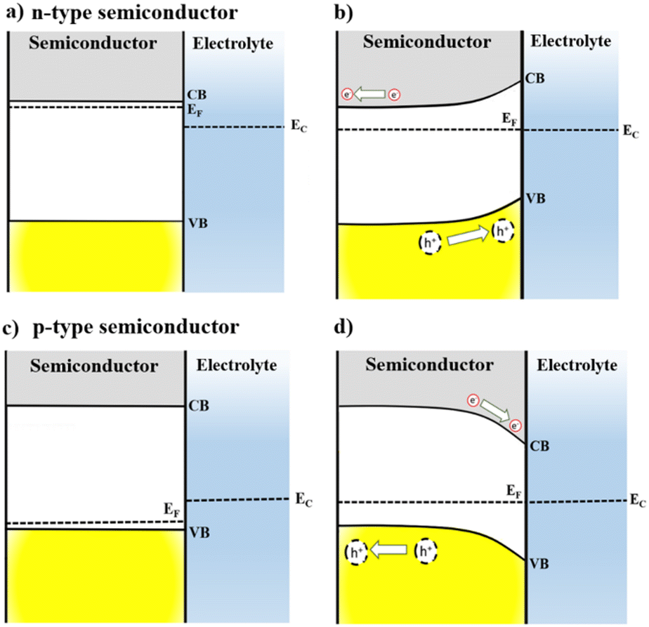 | ||
| Fig. 1 Energy diagrams for n-type and p-type semiconductor electrodes immersed in an electrolyte with electrochemical potential (EEC) at non-equilibrium (a) and (c) and in equilibrium (b) and (d) with the Fermi level of the semiconductor (EF). | ||
Conversely, for p-type semiconductors EF is located slightly above the VB; therefore, downwards band bending will take place as a result of electron transfer at the space charge layer to achieve the electrochemical equilibrium. The electric field generated from downwards band bending is the key to a p-type semiconductor for operating as a photocathode: under irradiation, electrons will flow towards the semiconductor surface, being available to perform reduction reactions. The band bending can also be modulated by application of an external electrical potential to the electrode. Additionally, polarization can enhance the separation of the photogenerated carriers at the semiconductor/electrolyte interface and improve the current flow.4
A typical PEC cell is constituted by at least one photo-responsive semiconductor electrode, that uses the photogenerated carriers to promote redox reactions. The application of a semiconducting material as a photoelectrode in a PEC cell depends on the relative positions of the CB and VB edges to promote reactions of interest, such as H2 production from water, CO2 reduction, and others. Fig. 2 shows examples of some semiconductor oxides and their CB and VB relative positions.
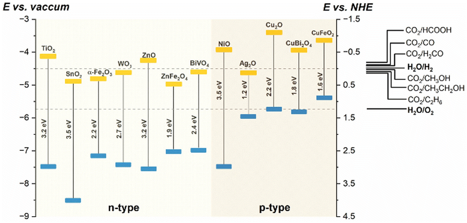 | ||
| Fig. 2 Relative CB and VB edge positions (yellow and blue rectangles, respectively) for some semiconductor oxides in aqueous solution (pH 0), and the potentials of reactions of interest versus vacuum (left) and NHE (right).16–19 | ||
2.2 Evaluating the efficiency of photoelectrodes in PEC cells
Understanding of photoelectrode abilities for solar energy conversion requires several studies. The measurements of incident photo-to-current conversion efficiency (IPCE) consist of the ratio of incident photons that are converted in electrical current. The IPCE maximum can usually be associated with the Eg and is also affected by the redox reaction kinetics and charge generation, separation, and transport processes. The IPCE is estimated under monochromatic irradiation, as represented by (eqn (1)).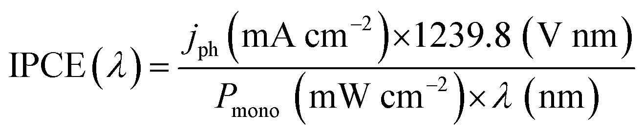 | (1) |
Here it is important to mention that the “maximum theoretical photocurrent” is a value calculated assuming that every photon with energy ≥Eg is absorbed and generates an exciton that is collected without recombination (thus, disconnected with particular reactions).10
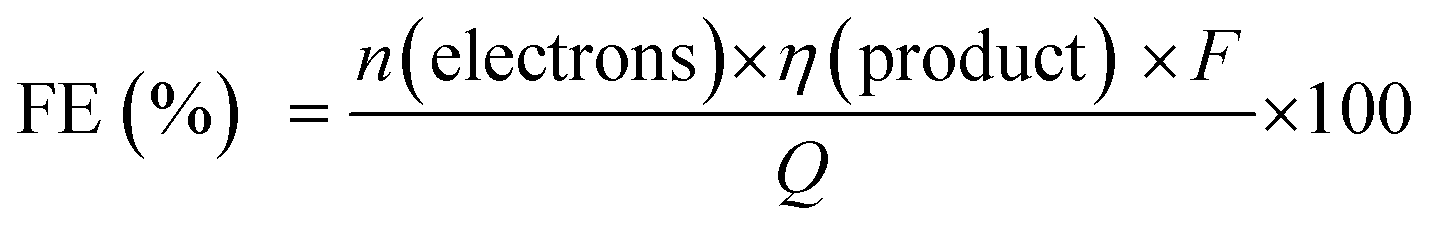
The PEC cell efficiency, which depends on the photoelectrode activity, can be evaluated considering the current flow and the production rate of gaseous or liquid molecules with time. The faradaic efficiency (FE) for each product can be estimated using eqn (2) considering the amount of produced substance (η), the amount of electrons involved in the redox reaction (n), and the total charge passed through the external circuit (Q), where F is the Faraday's constant (96485 C mol−1).2
 | (2) |
When different products are obtained, the FE indicates the system selectivity for every product and allows us to discuss possible side reactions (including photocorrosion). For instance, the hydrogen evolution reaction (HER) is an important side reaction that decreases FE of solar fuel production from the photoelectrochemical reduction of CO2.
Finally, the solar-to-fuel efficiency (STF) can be calculated from eqn (3), considering the rate of fuel production (rfuel, in mmol s−1), the standard Gibbs free energy of product formation (ΔG0, in kJ mol−1), the power density of incident irradiation (P, in mW cm−2), and the geometric area of the photoelectrode (A, in cm2).20
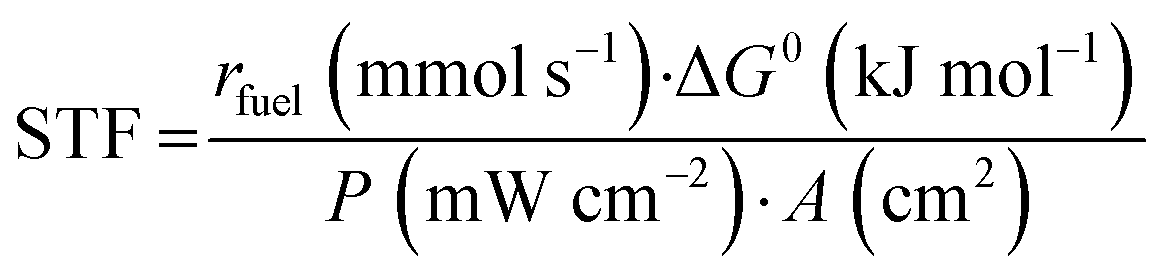 | (3) |
2.3 Considerations on the stability of photoelectrodes in PEC cells
The successful application of a photoelectrode in PEC cells also depends on the semiconductor stability under the practical conditions of PEC cell operation. The electrolyte pH and composition, applied potential, and irradiation processes may affect the photoelectrode long-term stability. Bismuth vanadate (BiVO4), for instance, an n-type semiconductor, is largely used as a photoanode for the oxygen evolution reaction (OER) only under mild pH conditions (pH 5–9), since it is soluble in strongly alkaline media (pH > 11). In contrast, the n-type semiconductor α-Fe2O3 is suitable for alkaline conditions.8The irradiation process can also affect the photoelectrode stability because the photogenerated e−/h+ pair may cause self-photocorrosion in some semiconductors. For instance, cuprous oxide (Cu2O), a p-type semiconductor, presents photocorrosion upon illumination in aqueous medium, which results from simultaneous self-oxidation to copper oxide (CuO) and self-reduction forming metallic copper (Cu). Toe et al. investigated the Cu2O photocorrosion pathway using e− and h+ scavengers and concluded that self-photooxidation (Cu+ + h+→ Cu2+) is the main cause of Cu2O degradation.21
Usually, the long-term stability of a photoelectrode can be evaluated by monitoring the generated photocurrent within time, and by observing the rate of product formation. The semiconductor surface morphology and crystal structure should also be monitored before and after utilization in PEC cells using X-ray diffraction (XDR), X-ray photoelectron spectroscopy (XPS), scanning electron microscopy (SEM), and/or transmission electron microscopy (TEM). These studies contribute to the understanding of materials instability and can help to develop strategies to enhance the semiconductor electrode long-term stability.22
3. Synthesis aspects
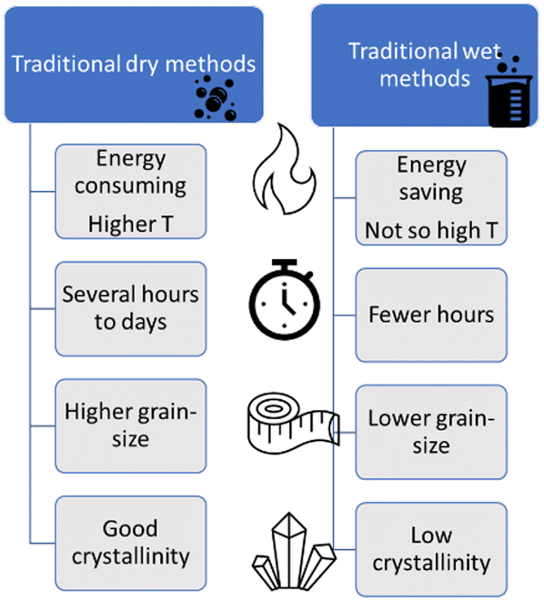
The overall PEC performance of semiconductor electrodes depends on both intrinsic and tuneable characteristics of materials, such as defects and surface aspects.23 In particular, the materials nanostructuring can provide an increase in the surface area; an improvement in the electron–hole diffusion processes; mitigation of electron–hole recombination, etc.24 These features, and consequently the final properties of the electrode, are synthesis-dependent. The choice of an appropriate synthesis method relies on good previous knowledge of the different techniques available and on the influence on structure, phase stability, and characteristics of each material.The synthesis methods can be classified in two large categories: (i) “dry methods” (solid phase), for those processed without solvents; and (ii) “wet methods”, for those with a major component in the liquid phase.
Solid-phase reactions usually require extreme conditions to overcome thermodynamic barriers and compensate the low diffusion transport of reactants. Wet synthesis routes (or solution based), instead, generally take place under milder conditions, like lower temperatures, since transport in the liquid phase is favoured.25 The main appeal of solution based methods is the simultaneous generation of several stable small nuclei, resulting in (mono) dispersed nanoparticles (NPs). However, these NPs can suffer Ostwald ripening, which implies the smaller particles precipitate onto larger ones, increasing the final particle size.26
The choice of synthesis method will depend, mainly, on the final application and on the technical apparatus available. In this work, we will comment on the most feasible and common techniques for semiconductors production, as well as some less practiced, but possible alternatives, here named “unconventional dry and wet methods”.
3.1 Traditional “dry” methods
Among the most traditional methods to produce ceramics, one finds solid-state reaction (SSR) and milling, which can be used independently or in combination.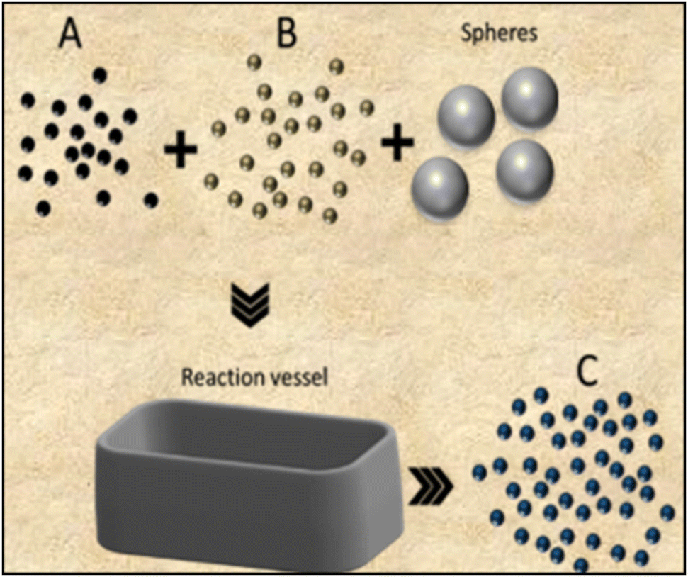 | ||
| Fig. 3 Schematic cross-sectional representation of the milling process for synthesizing smaller-sized powder products from reactant mixtures. | ||
The grinding process is driven by high energy collisions among the spheres and the reactants, resulting in size reduction of the micro crystallites into highly homogeneous nanometric structures, with or without chemical reactions.28 There are a wide variety of ball mills (cup, friction, shaker, vibration and planetary), constructed with dense materials such as tungsten carbide, steel, or zirconia.29
Beyond ball mills, there are other types of mill apparatus. One of them is the stirring mill, which is preferable for faster and highly energetic reactions, and when only small amounts of precursor (in the order of a few grams) are available. In other ways, dry milling is an appropriate strategy to induce chemical reactions in the synthesis route. The appropriate choice of the pulverization process even brings some interesting properties to ground material.
In general, high-energy grinding can be considered an environmentally friendly, reliable, reproducible, and easy-to-use process with low costs. This is due to the possibility to use easily accessible raw materials on its powder form. However, the milling process has its own limitations that can affect the final properties of the desired product, such as agglomeration of powders and cross-contamination from mills.
Complex oxides can also be obtained using these methods. As an example, in a recent work, Wang et al.30 reportedly obtained vanadium–zircon (V–ZrSiO4) from a first mix and grinding of precursors followed by calcination of a precursor mixture at high temperature, in this case, 500 to 900 °C for some hours.
3.2 Traditional “wet” methods
The traditional solution-based methods used to produce complex oxides include sol–gel, hydrothermal and electrodeposition. As these are well-known methods for synthesizing materials, we will just briefly comment on the general aspects of each one.Semiconductor oxides can be directly obtained via co-precipitation, when the precipitate is itself the desired oxide, and thermal treatment is only for crystallinity improvement, or indirectly, when precipitated as a precursor that is further thermally converted into the final oxide. Saib and collaborators precipitated AgCoO2 nanocrystallites (∼20 nm) from Co3+/Ag+ aqueous solution, using NaOH as the precipitant agent, at relatively low temperature (80 °C).31 They observed that the product is a p-type semiconductor with possible application as a photocathode for the HER. In another work, Priya et al. firstly precipitated a sample of mixed hydroxides from a Bi3+/W6+/Fe3+ aqueous solution employing NH4OH as the precipitating agent, with posterior solvothermal treatment (160 °C/24 h) and annealing at 600 °C, resulting in BiFeWO6 nanoparticles.32
To sum up, co-precipitation is a simple route, with several advantages such as no necessity of expensive equipment and reagents, good control of precipitated properties, and compatibility to large-scale industrial production. The limitations include the absence of precise temperature control, time-consuming protocols for some syntheses, yield limited by precursor solubility and the recurrent necessity of additional steps for purification and post-treatments.33
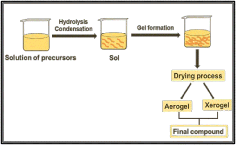 | ||
| Fig. 4 Schematic representation of the sol–gel procedure for the preparation of a compound from precursor solutions. | ||
One key advantage is the presence of an organic precursor matrix, that ensures the mixture of different metals on an atomic scale.35 However, in the synthesis of ternary or quaternary oxides, the different hydrolysis rates of precursors can lead to phase separation during the condensation step, which can prevent the achievement of multicomponent oxides. Then, small molecules such as citric acid and acetylacetone can be employed to form stable aqueous metal complexes, decreasing the hydrolysis rate of reactive precursors.35,36
The sol–gel process also requires thermal post-treatments to remove organic residues and hydroxyl groups on the surface of the desired crystalline material, causing some difficulties related to non-uniform heating and undesired reactions with ceramic crucibles.37 However, this synthesis technique presents several advantages including low cost, low temperature (soft chemistry), simple experimental set up, and allowing a high control of parameters (pH, concentration of reactants, nature of solvent, type of additives, aging of solution, and others).36,38
Furthermore, major drawbacks found in the conventional sol–gel method were overcome with non-hydrolytic sol–gel chemistry. In this process, the condensation step is carried out in non-aqueous media with an oxygen-donor other than water (e.g. ethers, carboxylates and alcohols). Non-hydrolytic conditions allow more controllable kinetics compared to traditional hydrolysis reactions, resulting in better control of the crystallization phase, in particular of pure multi-metal oxides.39
Sheikh et al. synthesized a composite of BiFeO3 and La2NiMnO6 to be used as the photoanode for water splitting with improved PEC performance (∼14.07 mA cm−2 – more than 50% increase in comparison to the bare BiFeO3 in the same work) and a maximum photon-to-current conversion efficiency of ∼9.61%.40 In another work, Xie et al. prepared a W:BiVO4–FeCoW heterojunction with sol–gel followed by post-annealing. The photoanode exhibits a photocurrent which is enhanced to ∼3.8 times that of a W:BiVO4 photoanode at 1.23 V vs. the reversible hydrogen electrode (RHE).41
HT and ST are among the main methods for fabricating nanostructured and advanced materials, providing an excellent environment for crystal growth with control over size and morphology, with the formation of monodispersed NPs. Additionally, HT processing brings several other advantages, such as lower sintering temperatures and reaction times, when compared to traditional ceramics synthesis methods; the obtainment of products with higher purity and good homogeneity; narrow particle size distributions; crystal symmetry and even the possible formation of metastable compounds.42 HT/ST are also possible alternatives to produce materials that cannot be synthesized using traditional ceramic methods with controllable size and morphology, due to the evaporation of reactants, or metastable structures with special valence states.42,43
Again, surface aspects, like morphology and particle size, can be tailored by varying the different reaction parameters, such as time, temperature, pressure, pH, concentration of reactants, capping agent, etc.44 Recently, a review by Wu et al. discussed ternary Bi-based oxides like γ-Bi2MoO6, Bi2MoO6, and Bi2WO6 obtained using HT and ST methods.45 In another work, a dumbbell morphology of CaBi2O4, with submicrometric sizes of 300 nm diameter and 500 nm length, was obtained. When electrodes of this semiconductor were applied for PEC water splitting, a photocurrent of 0.83 mA cm−2 at 1.23 V vs. RHE was generated without hole scavenger, and 1.19 mA cm−2vs. RHE using Na2SO3 as the hole scavenger.46
Due to these advantages, there are a significant number of studies reporting the synthesis of complex oxides and their composites using hydrothermal methods. The main drawbacks rely on safety concerns (the internal pressure in the stainless-steel vessel must be controlled) and the process scale-up (adaption of the equipment for larger volumes operation).
Fig. 5 displays a scheme of different electrodeposition procedures. The electrodeposition can be carried out either under potentiostatic control, by setting a constant voltage between the working electrode (WE) and reference electrode (RE), while the current flows between the WE and auxiliary electrode (AE) (Fig. 5(a)). The applied voltages are higher than equilibrium potential (overpotential) to overcome reaction kinetics limits. The key advantages of the potentiostatic mode are film purity and the adjustable atomic ratio of the electrodeposited elements, which have great impact on the semiconductor properties (n or p-type).48
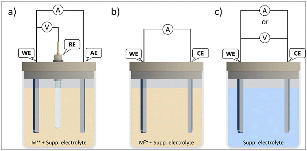 | ||
| Fig. 5 Electrochemical cells setup for electrodeposition through: (a) potentiostatic, (b) galvanostatic, and (c) anodization procedures. WE – working electrode; RE – reference electrode; AE – auxiliary electrode; and CE – counter-electrode. | ||
The electrodeposition can also be achieved under galvanostatic control with the electrical current between the WE and CE (counter-electrode) kept constant. Then, only two electrodes are required (Fig. 5(b)) and the cell potential is not equal to the WE potential. The potential fluctuation can be attributed to changes in WE conductivity, due to semiconductor film growth, and to the decreasing of the ionic activity of precursor in the electrolyte during the electrodeposition process. Thus, side reactions can take place to maintain the current value, which can impact the purity and properties of the deposited film. In good practices, either the cell or WE potentials should be monitored, to avoid damage in the electrodes or solvent decomposition.49
There is another approach, the anodization mode, that uses the conductive substrate itself as the metal ion source. This method has been applied as a reliable way, e.g., to produce vertically aligned nanostructures and nanoporous films. The synthesis is processed in two electrode-cells (Fig. 5(c)), where the WE is the anode (so the term anodization is used). The film formation is generally modelled as a process of field-assisted oxidation, and the nanostructures grow due to the migration of ions from the substrate into the interface due to an electric field, in an electrochemical dissolution reaction, followed by precipitation. These oxidations can be achieved under either current or potential controlled modes. Potentiostatic regimes are the most used, due to the easiness of morphology control. The syntheses of metal nanotubes often use potentials in the range of 5 V to 30 V in water or even more in organic solvents.50 The main drawback of anodization is the fact than not all metals and alloys can be used, only a few, that can form passivation layers (valve metals) (e.g. Ti, Al, Nb).51
Despite the simplicity, the solvent, pH, metal precursor and electrolytes play important roles in electrodeposited material properties. For instance, water is the most used solvent, however it has a limited potential range of 0 V to +1.23 V (vs. SHE), which are related to HER and OER, respectively. Thus, if the potential of interest is close or over these limits, the faradaic efficiency may decrease. Precursor solubility is also an important point to consider. Commonly used non-aqueous solvents are ethylene glycol, DMSO and acetonitrile. Although most electrodepositions are performed under room conditions, temperature is another factor that can be optimized, since some reaction kinetics are slower than desired. Although a temperature rise implies faster deposition, it must be carefully controlled, otherwise the film is formed too quickly, with poor uniformity and adhesion on the substrate.52
Although many semiconductor oxides are directly synthetized with high quality and crystallinity, it is not always possible to co-electrodeposit metals to produce multinary film oxides. In some cases, the compound is synthetized as a precursor (i.e. hydroxides), which further undergoes thermal treatment to improve its crystallinity, or to chemically produce a more complex compound. An example is iron oxyhydroxide (FeOOH), which has been synthetized using different electrochemical routes,53,54 and further converted to α-hematite (α-Fe2O3) via annealing. These combined techniques can also be used for the synthesis of more complex multimetal oxides. For instance, Labchir et al. demonstrate the formation of a cobalt ferrite (CoFe2O4) film by mixing the cation sources of Co2+ and Fe2+ precursors in the electrolyte, followed by heating (24 h at 500 °C).55
In summary, the electrodeposition method is a simple, versatile, and relatively low-cost method, generally performed under mild conditions, such as room temperature and atmospheric pressure. Although poor practices can lead to non-uniform film thickness and low adhesion, effective methodologies allow the fine control of deposited film composition, thickness and morphology, resulting in films with excellent adhesion and uniform electrical contact to the substrate.
So far, we have reviewed the most used “dry” and “wet” methods for the preparation of complex oxides. A direct comparison among these methods is not straightforward. Furthermore, the synthesis choice must consider the target material and the available resources. Regarding some “dry” methods, like SSR, the oxides of interest are generally obtained with good crystallinity, but also with large and irregular grains. Then, milling post treatments are required to improve the adhesion and the electrical contact to the electrode substrate surface (like fluorine-doped tin oxide – FTO). Conversely, wet methods, like HT, generally produce well-defined morphologies and smaller sizes, but with lower crystallinity, requiring posterior annealing steps. Finally, the methods that can directly generate the oxide phase on the substrate, like electrodeposition, or even HT, when the FTO is placed with the precursors inside the autoclave, tend to form oxide films with adequate electrical contact with the substrate, a required characteristic for electrodes. Fig. 6 summarizes the comparison between general “dry” and “wet” techniques. In the next section we discuss some less investigated, but possible techniques for the preparation of PEC materials.
 | ||
| Fig. 6 Comparison of the main aspects involved in traditional “dry” (solid-state reaction and milling) and “wet” (co-precipitation, sol–gel, solvothermal and electrodeposition) synthesis protocols. | ||
3.3 Unconventional “dry methods”
3.3.1.1 Pulsed laser deposition (PLD): a type of PVD. PVD uses high power energy sources to melt, evaporate and ionize the surface of a target material under ultra-high vacuum conditions. Initially, the material is ablated by a high energy source, which produces a plume of the target's constituents. Then, the “vaporized” atoms are transported to the substrate to be coated. Generally, this is carried out under ultra-high vacuum conditions.56
PLD, a particular type of PVD, uses a laser with a high-power density and narrow frequency bandwidth as a source for vaporizing the target material. This technique was first used by Smith and Turner, in 1965, for the preparation of semiconductors and dielectric thin films.57 Later, in 1987, the technique was established with the work of Dijkamp and coworkers at high temperature, which generally occurs in straight paths.58 The plume of vaporized material reacts with the appropriate gas during the transport stage (which may be oxygen, nitrogen, or methane) and deposits on the substrate. This technique is particularly used for thin film preparation: the material ejected from the target is collected on a previously selected substrate on which it condenses, and the thin film grows,59 as represented in Fig. 7.
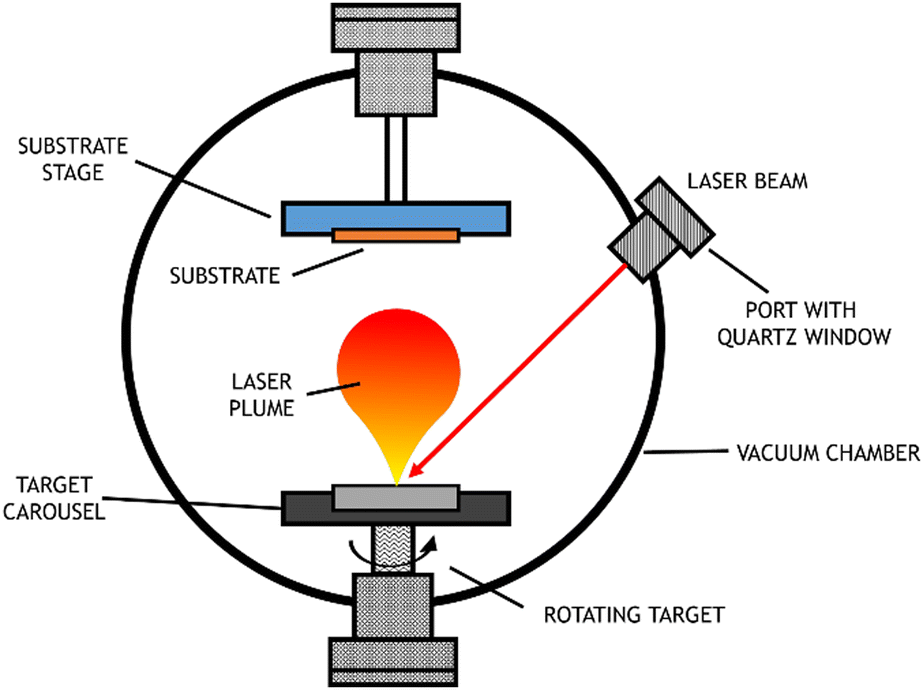 | ||
| Fig. 7 Scheme of pulsed laser deposition equipment. | ||
When the objective is the production of electrodes, a conductive substrate is used; for example, to obtain thin films of metallic oxides, nitrides or carbides, the target should consist of metals or even ceramic materials with that chemical composition. The films produced using the PVD technique have interesting characteristics, such as a high level of hardness and resistance to wear, friction, and oxidation. A review from 2019 focused on synthesis for water splitting materials and reported PVD techniques to obtain single crystalline thin films with improved properties.60
The PLD technique has many advantages in the growth of thin films over other techniques. Among them are the easiness to form compounds with controllable stoichiometry, the high deposition rate, and the control over the film thickness. The fact that the laser is used as an external energy source results in a process where the surface is extremely clean and free of contaminants. However, there are many variables that can affect film properties, such as laser fluency, background gas pressure, and substrate temperature.
PLD can be employed for the growth of multilayers of different chemical compositions with an epitaxial relationship between domains. This kind of approach is quite satisfactory to produce photoelectrodes containing heterojunctions, where the contact between the crystalline structures of the different domains must be closely interconnected. In the next section, we discuss a case of successful synthesis of a ternary oxide, CuBi2O4 on a template via this epitaxial growth.
Although the advantages are quite attractive,61 and the technique could be successfully applied for the direct production of complex multication oxides such as the challenging structure of Ba2Co2Fe12O22,62 the technique has some challenges to overcome, which limits the use of PLD mainly in academic and small-scale studies, (typically ∼ 1.0 cm2) preventing its industrial widespread use.63
3.3.1.2 Chemical vapor deposition (CVD) and atomic layer deposition (ALD). Chemical vapor deposition (CVD), defined as the deposition of a solid on a heated surface from a chemical reaction in the vapor phase, has been a well investigated technique since the mid-1960s, progressing very rapidly in recent decades.64 Unlike PLD techniques, CVD is a part of many industrial manufacturing processes used to produce semiconductors and many other material types.65
The CVD process can involve many chemical reactions and events, that can basically be described in the following sequence: ① reactant gases enter the reactor by forced flow and diffuse through the boundary layer; ② gas adsorption occurs at the substrate surface; ③ a deposition reaction takes place; ④ desorption of reaction gaseous by-products occurs and ⑤ by-products diffuse away from the surface, through the boundary layer. These events are summarized in Fig. 8.66,67
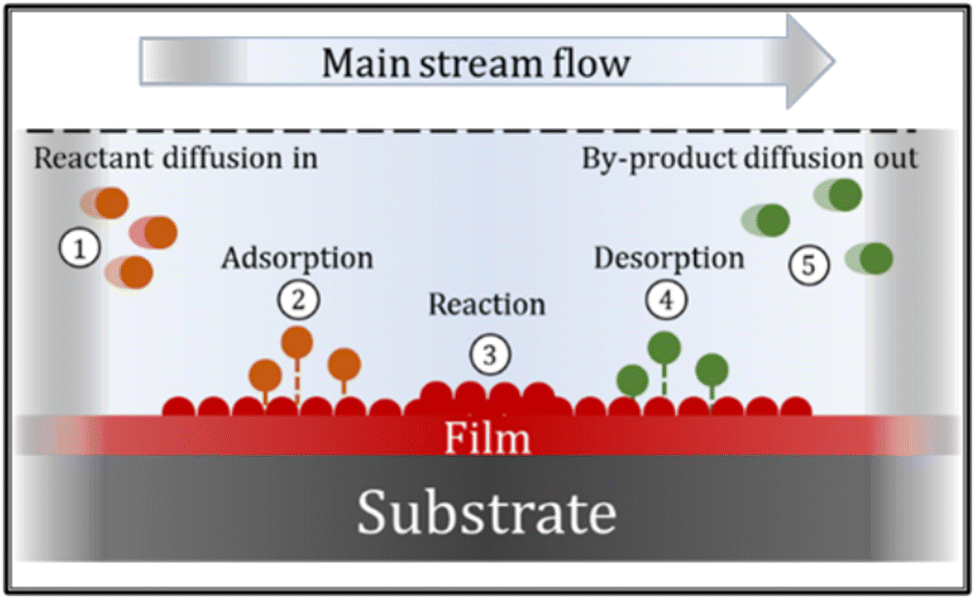 | ||
| Fig. 8 Sequence of events during the chemical vapor deposition process. | ||
CVD is a relatively simple and economically competitive technique that allows the coating of surfaces of any shape and various sizes, also permitting changes in deposition rates, chemical composition and co-deposition of elements or compounds. Different from PVD processes, the CVD equipment does not normally require ultra-high vacuum and is not restricted to a line-of-sight deposition. Generally, CVD is a single operation and an integral part of a manufacturing process, particularly in microelectronics. Most manufacturers have their own CVD facilities, which makes it difficult to implement a unified experimental setup.66
The microstructure varies depending on the material to be deposited. In general, ceramics obtained by CVD, such as SiO2, Al2O3, Si3N4, and most dielectric materials tend to be amorphous or, at least, have very small grain microstructure. On the other hand, deposited metals tend to be more crystalline. The crystal size of the deposits is also a function of deposition conditions, especially temperature. Moreover, through the pressure control, it is possible to control the thickness of the boundary layer and, consequently, the degree of diffusion.68
In 2006, Grätzel and co-workers synthesized thin films of silicon-doped α-Fe2O3 deposited by atmospheric-pressure CVD from Fe(CO)5 and tetraethoxysilane on SnO2-coated glass at 415 °C. As a result, they obtained dendritic nanostructures with excellent performance as a photoanode for water splitting in 1 M NaOH, that exhibited 42% of IPCE at 370 nm and 2.2 mA cm−2 in AM 1.5G sunlight of 1000 W m−2 at 1.23 VRHE.69
The synthesis of complex oxides by CVD is possible, as there are adequate precursors for each metal present in the final oxide. The reactants must then be highly volatile molecules, which is a problem for some electropositive ions that tend to form ionic compounds. However, some alternatives are possible, as reported by Bekermann et al. to obtain the superconductor YBa2Cu3O7: volatile molecules of the metal precursors were substituted by their complexes, such as yttrium with 2,2,6,6-tetrametil-3,5-heptadione, allowing the use of CVD.70
Despite several advantages, the high operating temperatures of the CVD technique (above 600 °C) are among the main drawbacks since many substrates are not thermally stable at these temperatures. Improvements of deposition conditions and precursor properties, such as Metallo-Organic CVD and plasma-enhanced CVD, partially compensates this problem, but it makes the process more expensive. Another challenge is the need for chemical precursors with high vapor pressure, which are often dangerous and sometimes extremely toxic. The by-products of CVD reactions can also be toxic and corrosive and must be neutralized, which can be a costly operation.60
In conclusion, the CVD technique allows the deposition of thin films on conductive substrates and, although not yet widely used for photoelectrodes synthesis, has great potential for this purpose.
In contrast, atomic layer deposition (ALD), a very close process to CVD, has recently attracted much attention for PEC applications, due to its unique nature for precise control over film thickness and growth of complex nanostructures. ALD is based on a gas–solid reaction where the adsorbed molecules in each reaction cycle is one monolayer, resulting in a layer-by-layer growth mechanism.71 The deposited film can act, then, as a protective layer, or by increasing the absorption range of the solar spectrum, also by decreasing the recombination rate of photogenerated charge carriers.
A good example, reported by Paracchino and coworkers is the correlation of the ALD deposition temperature of Al:ZnO and TiO2 protective layers and their band energy positions, a critical factor to enhance carrier separation.72,73 ALD is an ideal technique for the deposition of protective layers, uniformly sealing irregular surface topologies of nanostructured substrates such as Si nanowires, InP nanopillars, and cubic Cu2O with structures.
3.4 Unconventional “wet methods”
In this sense, microwave equipment can be an excellent alternative to conventional heating. Microwaves, which are electromagnetic energy with a frequency in the range of 300 MHz to 300 GHz, interact with materials via two mechanisms: dipole interaction and ionic conduction. Microwave-assisted techniques show efficient heat transfer and can be a fast, clean, low-cost, and environmentally friendly approach to produce high yield advanced materials.74
HT and ST are the most common microwave assisted methods, with the substitution of a traditional oven by a microwave source. A simple microwave oven can be adapted and employed in several types of “wet” methods to improve the synthesis efficiency with much shorter periods of time. The microwave-assisted HT was used to produce a nanocomposite of In2O3/ZnO and resulted in flower morphologies with petal diameters of 30 nm that exhibited PEC degradation of methylene-blue dye under visible-light.75
Microwave heating is also used in solventless reactions. Houl et al. prepared porous hematite photoanodes with wormlike networks using hydrothermal deposition and microwave-assisted rapid annealing of a β-FeOOH nanocube film on the FTO.76 According to the authors, since FeOOH, Fe2O3 and graphite are good microwave absorbers, the rapid conversion of FeOOH into Fe2O3 could be achieved through rapid microwave-assisted annealing. Furthermore, the water elimination derived from the constitutional OH groups in FeOOH would facilitate the formation of uniform pores in Fe2O3, resulting in a hematite electrode that exhibited an enhanced performance for PEC water oxidation, with an IPCE of 51% at 340 nm at 1.23 V vs. RHE.
While microwave heating can be very time and energy saving, the technique requires adaptation of the equipment (especially when used in combination with the hydrothermal method) which can bring safety issues, and due to the rapid annealing, the final products can present defected or non-well-defined morphologies.
The origins of SCS go back to the materials chemistry in mid-1980s literature. Though the invention of this process was recently claimed by some authors regarding a patent, the credits must be given to Ravindranathan and Patil who first observed the formation of metal oxides from the thermal decomposition of multiple metal organic complexes.79
In a broader sense, combustion can be defined as the reaction between a fuel and an oxidizer, which reacts rapidly with each other in a highly exothermic process, in most cases forming gaseous species as products. In SCS, metal oxides particles are obtained due to some particularities, such as: (i) the fuel is an organic complexing agent, which binds to metal cations and forms metal–ligand adducts; (ii) the oxidizer is a chemical agent added to the reaction mixture; (iii) both oxidizer and (metal-bound) fuel are not directly mixed; instead, both species are solubilized in a solvent, water being most commonly used.
After metal salt, fuel and oxidizer are dispersed in solvent, the reaction mixture is placed in a cup or crucible, which is then heated in a furnace or hot plate until the activation energy for the combustion reaction is achieved. The reaction occurrence is well-described as a multistep process. Given that the reactants are dispersed in a solvent, the first step needed is solvent evaporation, resulting in a solid (or gel) mixture of metal–fuel complexes and oxidizer molecules. This solid/gel mixture is further heated until the ignition temperature is reached, which will then start the reaction between fuel and oxidizer. The following step is a cascade of self-supported reactions which provides the entire energy needed for the SCS completion, as the temperature inside the reaction vessel can reach up to 1800 °C. A violent release of fumes (H2O, CO2, N2 and others) is observed at this point of the process, which will then proceed until depletion of reactants. The final product is usually a foamy, porous, and finely dispersed solid together with a multitude of solid contaminants/ashes which originate from incomplete combustion. A schematic diagram summarizing this process is shown in Fig. 9.80Table 1 summarizes combinations of metal salts, fuels and oxidizers used in a few representative works recently describing SCS of complex metal oxides.
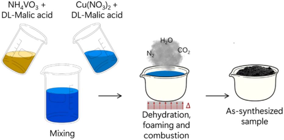 | ||
| Fig. 9 Schematic representation of SCS synthesis of copper vanadates. Adapted with permission from ref. 80 Copyright 2019 American Chemical Society. | ||
| Metal salts/oxidizer | Fuels | Product | Ref. |
|---|---|---|---|
| Co(NO3)2, Al(NO3)3 | Glycine, PVA, urea | CoAl2O4 | 85 |
| Mn(NO3)2, Zn(NO3)2, Fe(NO3)3 | Citric acid | (Co, Mn, Zn)Fe2O4 | 86 |
| Fe(NO3)3, Mg(NO3)2 | Citric acid | MgFe2O4 | 87 |
| M(NO3)x (M = Co, Fe, Mn, Ni, Al, Cr, Sr) | Glycine | LaMO3 | 88 |
| Cr(NO3)3, Cu(NO3)2 | Glycine | CuCrO2 | 89 |
| Cu(NO3)2, Zn(NO3)2, C4H4NNbO9 | Urea | CuNb2O6, ZnNb2O6 | 90 |
| Bi(NO3)3, NH4VO3, HNO3 | Citric acid, PEG 6000 | BiVO4 | 91 |
| Cu(NO3)2, NH4VO3 | DL-Malic acid | α-CuV2O6 | 92 |
As can be seen from Fig. 9 and the previous discussion, classical reaction parameters such as temperature and pressure are not exactly tuneable in SCS procedures. Meanwhile, after the onset temperature is reached, all the energy input for the oxide formation arises from the combustion reaction, at which the reaction temperature may increase to much higher values than the onset temperature, as shown for instance in the formation of iron oxide nanoparticles by the SCS reaction.81 The intense temperature peak is mainly associated with the formation of hypergolic mixtures of gases from the initial reaction between the fuel and oxidizer.82 In this sense, the most important reaction parameters to be tuned in SCS procedures are the nature of fuel and oxidizer and their ratio.
The reaction mechanism, thermodynamics, and kinetics, which are beyond the scope of this work, have been thoroughly studied, and the reader is referred to some review papers.83,84 Specifically for PEC applications, the SCS products show both positive and negative aspects that must be considered. While particle size and shape control stand as highly tuneable features in SCS, ash contaminants and a lack of control in oxidation states are drawbacks for some materials, in addition to reaction hazards. These aspects will be discussed in the following section and as should be noted, the main aspect underlying these features is the fuel/oxidizer composition and ratio. As mentioned before, organic fuels used in SCS procedures act as complexing agents to produce metal–ligand complexes. These interactions are well-known to have a profound influence on geometry/morphology during nanoparticle growth by sol–gel or hydrothermal synthesis and as expected, the same is observed for SCS.
The use of additives can also influence the morphological aspects of SCS products. Cobalt/iron oxide synthesized by SCS showed a dramatic increase in BET surface area when KCl is added to the precursor mixture.93 Depending on the KCl/fuel ratio, the obtained surface area was as high as 115 m2 g−1, a 10-fold increase when compared to the 11 m2 g−1 observed in the absence of KCl. Glycine was used as a fuel for all the experiments, so the mechanism proposed by the authors involves the formation of a KCl crust around each metal nucleation seed after solvent evaporation, which would in turn avoid aggregation while the system is at high temperatures. Though this alone was provided as a satisfactory explanation, no mention to binding energies or nucleation vs. growth dynamics was provided, which could give additional insights into the observed differences.
As the reader may have noticed, up to this point all the transition metal-based SCS-derived samples presented herein are constituted by cations at their most stable oxidation state, for instance Cu2+, Fe3+, Nb5+, and Bi3+. This should be expected, given that high temperatures and oxidant species are present in the reaction environment. Metals at intermediate oxidation states such as Cu+ and Fe2+ are rarely observed in samples obtained directly from SCS without any post-treatment. Nonetheless, some authors have shown it is possible to obtain lower oxidation states and even metallic particles, depending on the fuel/oxidizer ratio. By providing a fuel-rich mixture, the reaction environment after self-ignition of the precursor mixture can become a high-temperature mixture of reductant gases, such as NH3 and H2, among others.83
This can in turn be used to promote the formation of heterostructures which are interesting for general catalysis, such as mixtures of copper oxides with Cu cations at different oxidation states,94 nickel oxide decorated with metallic nickel domains,95 magnetite-containing iron oxides,96 and Ce3+/Ce4+ CeO2 nanostructures to name a few.97 However, it must be noted that precise control of multiple phases/oxidation states is not straightforward, and synthesis of pure-phase low valence complex oxides might not be achievable by SCS, depending on the compound family being studied. This can be seen even for monometallic oxides such as, for instance, copper oxides. As shown by Hossain et al., pure phase Cu+ oxide cannot be obtained over a broad range of fuel/oxidizer ratios (Fig. 10).98 Higher selective for Cu2O arises on slightly fuel-rich mixtures, but a small increase in fuel amount leads to the formation of metallic copper.
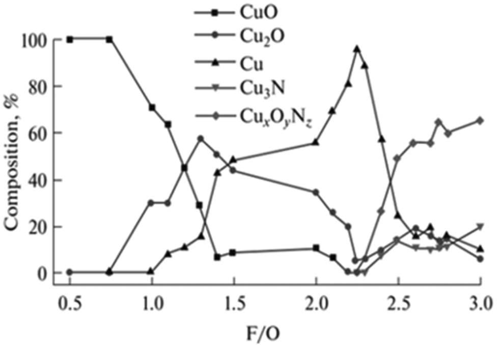 | ||
| Fig. 10 Product composition obtained from SCS synthesis of copper oxides with different fuel/oxidizer ratios. Reprinted (adapted) with permission from ref. 94 Copyright 2018 Allerton Press, Inc. | ||
Iron/aluminum spinel oxide, FeAl2O4, is an interesting case on lower oxidation state. The low-valency characteristic of iron cations in this structure is attributed to different reasons, such as a reductive environment and combustion of ionic liquids, with no further details on the mechanism or thermodynamics.99 Generally, iron oxides obtained by SCS usually provide structures with Fe3+ solely, such as LaFeO388 and MgFe2O4.87
SCS is a chemical reaction which occurs under extreme conditions, with significant evolution of heated gases. The amount of evolved gas can be estimated from the stoichiometric ratios of metal precursors and fuels. For instance, CuCrO2 is a representative example of the remarkable extension of gas evolution during SCS. Varga et al.89 propose the following chemical reaction using metal nitrates as precursors and glycine as fuel:
| 9Cr(NO3)3 + 9Cu(NO3)2 + 26C2H5NO2 → 9CuCrO2 +52CO2 +65H2O + 35.5N2 | (4) |
This indicates that, for each mole of CuCrO2 formed during SCS, 17 moles of high temperature gases (CO2, N2 and steam) will theoretically quickly evolve from the reaction vessel. As the authors indicate that the reaction temperature reaches values above 900 °C, it could result in 1.6 m3 of hot gases for each mole of CuCrO2, in a rough approximation using the Clapeyron equation. This estimative, though somewhat inaccurate, indicates a significant risk posed by gas evolution during SCS. To avoid incidents, some authors report the use of more sophisticated reactors for SCS rather than a lab beaker or crucible. Indium/gallium oxides were obtained by SCS using a mixture of metal nitrates and hydrazine,99 from which gaseous hypergolic mixtures can potentially evolve. In this case, a sophisticated reactor with gas flow, pressure/temperature control and a protective insulation was used, and the reader is referred to this work for a detailed design figure. Iron oxide was also obtained by SCS using a reactor with gas outlet and protective elements.81 Nonetheless, common beakers and crucibles are still frequently used for SCS, as can be seen in some recent papers.83,96,100,101 These references show representative photos of the evolution and outcome of SCS procedures and the reader is referred to those, to be aware of what infrastructure might be necessary to perform SCS at the lab.
Incomplete combustion is often observed in SCS systems, and the resulting byproducts can be different types of N,C-containing ashes. This means that one should pay special attention to washing procedures after SCS, to assure that no contaminants are present when the obtained oxides are applied, especially for PEC applications. The presence of carbonaceous contaminants can be misleading when one is performing CO2 reduction experiments, given that part of the detected products may originate from the conversion of carbon-containing molecules instead of CO2. It must also be noted that nitrogen incorporation into oxide structures has been observed, for instance in the case of copper oxides.94
To sum up, these non-conventional procedures also present advantages and disadvantages. However, it is possible to list some common features. Usually, methods that produce oxide films directly grown on the subtract generally result in electrodes with superior properties. However, as in the case of PVD methods, expensive equipment that requires ultra-high vacuum conditions are needed. Moreover, high temperatures can damage the substrate and precursors can volatilize, in the case of CVD. In contrast, solution combustion is operationally simpler, but is still not adequate for direct film preparation. Additionally, microwave assistance can solve long time exposure, but involves safety concerns with the adaptation of equipment. Thus, the choice of synthesis approach should consider syntheses conditions, apparatus, and final product. Fig. 11 is a scheme showing the intercessional features of each of the discussed less investigated methods for PEC applications.
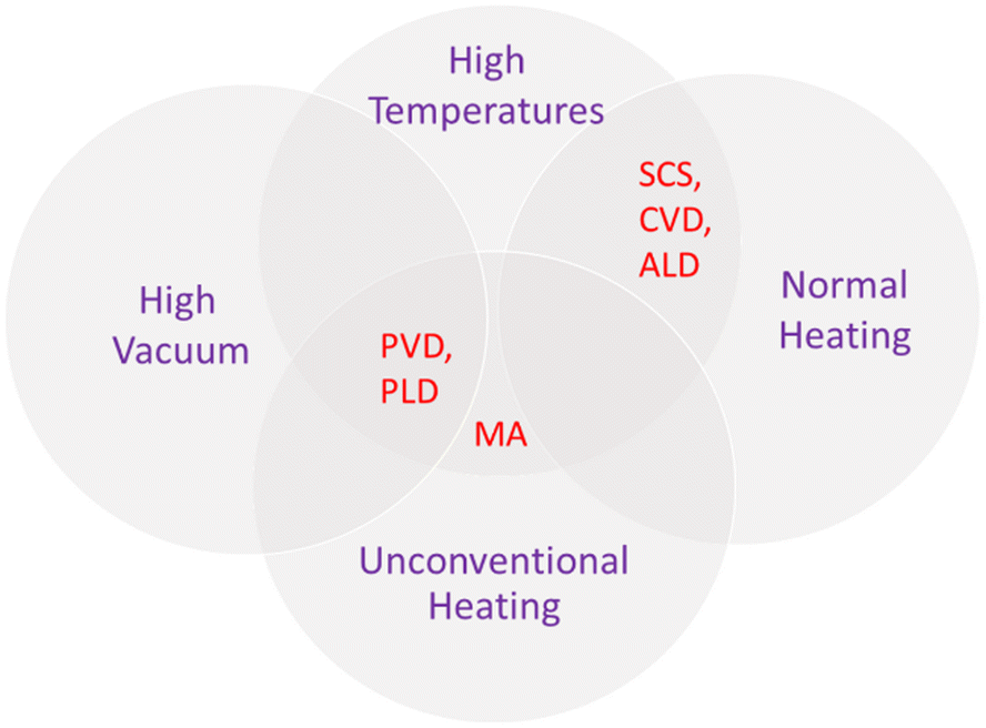 | ||
| Fig. 11 Scheme of intercessional features for unconventional dry (physical vapor deposition, pulsed laser deposition, chemical vapor deposition, atomic layer deposition) and wet (microwave-assisted and solution combustion synthesis) methods. | ||
4. Complex metal oxides – synthesis and challenges
In this section we discuss the current synthetic routes to obtain some of the promising complex oxides for application as photoelectrodes.4.1 BiVO4 and the ferrites for application as photoanodes for oxidation reactions
Bismuth vanadate, in the monoclinic crystallographic phase, is probably the most investigated complex oxide for PEC applications. The m-BiVO4 stands out as an n-type semiconductor with absorption in the blue-ultraviolet range of light (2.4–2.5 eV), suitable band edge position for water oxidation (EVB = +2.4 VRHE), long free photogenerated charge carrier lifetime (τ ≅ 40 ns, λ = 450 nm), few inherent recombination sites, and highly defect tolerant. However, intrinsic drawbacks such as short carrier diffusion lengths and relatively low carrier mobility (∼4 × 10⁻² cm−2 V−1 s−1 at 1 sun), prevent the achievement of its theoretical photocurrent (7.5 mA cm−2, AM 1.5G).102The performance of BiVO4 photoanodes can be enhanced using different strategies, such as surface morphology engineering, doping, heterojunctions, cocatalysts addition, or a combination of them. However, in this review, we will focus on the synthesis of pristine BiVO4, since extensive reviews on the methods to enhance the BiVO4 properties can be found in recent literature.103–105
Bismuth vanadate photoanodes can be obtained with good reproducibility by electrodeposition. The main protocol, which consists of the co-electrodeposition of vanadium and bismuth ions from the deposition bath, was first reported by Seabold and Choi.106 They correlated the electrodeposition time with film thickness and photocurrent density. Recently, Mohamed et al. also demonstrated that film thickness, light harvesting properties and electrochemical performances can be controlled by the electrodeposition time.107
Another electrodeposition-based methodology was developed by McDonald and Choi in which BiOI films are first electrodeposited.108,109 The further conversion into BiVO4 is achieved by the impregnation of this precursor with a vanadium source (VO (acac)2, NH3VO3) dispersed in an aprotic solvent, and posterior thermal treatment at temperatures up to 450 °C (eqn (5)). To date, this is still the most used route to build up highly active photoanodes. An interesting feature of photoanodes synthesized from BiOI precursor is high porosity, an inherited characteristic from void space between the 2D structure of BiOI plates. In an extensive work, Tolod and co-workers performed a deep investigation into how the synthesis factors, such as electrodeposition time, bath composition and calcination temperature, affect the BiVO4 film performance for the OER.110 They found that the photocurrent densities, and other parameters like onset potentials, charge transfer resistance and density of donors were dictated by the following characteristics: crystallite size, film thickness and porosity.108
| 2BiOI (s) + 2V5+ (s) + 3O2(g) → 2BiVO4 + I2(g) | (5) |
Although not mentioned yet, successive ionic layer adsorption and reaction (SILAR) is a layer-by-layer type methodology to grow films. In general lines, SILAR is a multistep dip-coating impregnation, where it is possible to easily modulate the film thickness. As demonstrated by Yassin, Sin and Jennings,111 and then by Seong and co-workers,112 the direct deposition of BiVO4 is achieved by reacting ammonium vanadate bismuth nitrate solutions on a conducting substrate. The authors observed that the as-synthesized films possess a porous texture, composed by fused particles with a size lower than 150 nm, and adjustable thickness in the range of 2 to 5 μm. These two steps are considered as one SILAR cycle. In this process, the film thickness will be proportional to the total number of deposition cycles. The advantages of this technique when compared with electrodeposition are the absence of an electrical power source, and the use of simpler precursor solutions. Fig. 12 is a scheme showing the main BiOI precursor methods discussed here. In the insets it is possible to see the SEM morphology change observed due to the transformation of BiOI to BiVO4 because of the step in Fig. 12(c), which is common after treatment with both electrodeposition and SILAR methods.
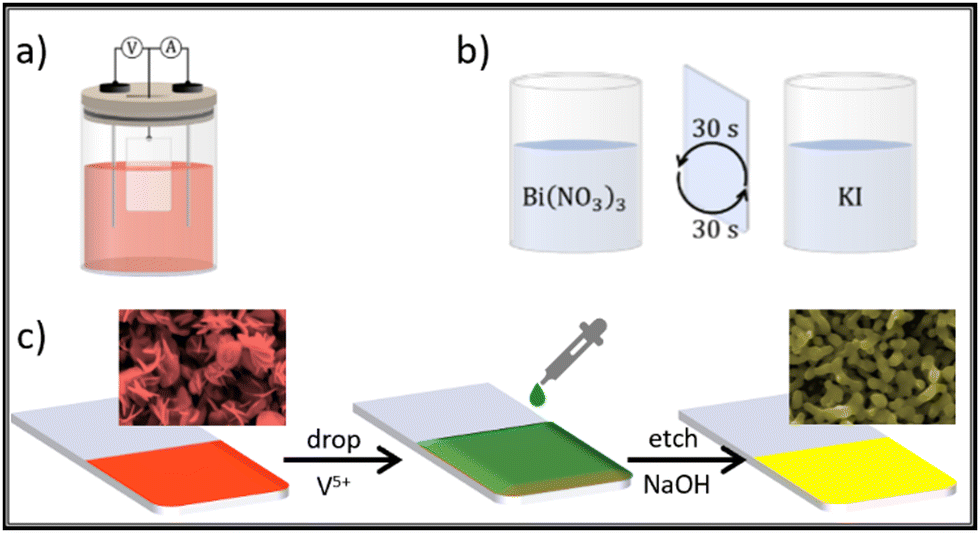 | ||
| Fig. 12 BiVO4 synthesis via BiOI template through: (a) electrodeposition; (b) SILAR; and (c) drop cast of V precursor for thermal conversion BiOI → BiVO4 common to both approaches. | ||
Deposition of the complex oxide film directly on a conductive substrate is very appreciable in terms of adherence and electrical contact between the semiconductors phase and the substrate, important characteristics for photoelectrodes. However, some articles also report the production of BiVO4 particles via traditional wet-synthesis methods, and its posterior deposition on appropriate substrates, like FTO. Samsudin et al. modulated the BiVO4 morphology by playing with a wide range of pHs and temperatures using HT synthesis and then the obtained particles were deposited on FTO via a doctor blade.113 Among the 13 variations, the sample synthesized at pH = 1.96 and 120 °C presented micro flower morphology with 1–2 μm leaf-like structures. Under an applied potential of 0.7 V vs. RHE, the resulting photoelectrode rendered the highest photocurrent density, 5.66 mA cm−2, producing 9.52 mmol L−1 of hydrogen in the counter electrode, within 7 h. This study shows an interesting correlation of PEC performance and semiconductor morphology (influenced by synthesis procedure).
Sol–gel was also performed for the preparation of BiVO4 photoelectrodes. Hilliard et al. produced semi-transparent BiVO4 thin films by dipping FTO on bismuth nitrate(III) and vanadyl acetylacetonate dispersed on a mixture of acetic acid and acetylacetone.114 The electrodes consisted of 10-layer BiVO4 films, 75 nm thick, exhibiting a photocurrent of 2.1 mA cm−2 (1.23 V vs. RHE) with 85% of faradaic efficiency for the OER in neutral pH. Shim et al. introduced polyethylene glycol (PEG) as a strategy to produce nanoporous BiVO4 photoanodes doped with molybdenum and observed that both PEG molecular weight and annealing temperature affected the final particle size, which varied from 50–150 nm. The photoanodes could generated 4.5 mA cm−2 of photocurrent (1.23 V vs. RHE) for 10 hours.115
Considering “dry-methods”, synthesis protocols of metal oxides involving a combination of milling and annealing are often found in the literature. Domen and co-workers reported highly crystalline BiVO4 structures with an average size of 300–500 nm using a combination of a SSR, ball milling and then, annealing (the thermal treatment was used to improve crystallinity). The resulting crystalline BiVO4 photoanode generated a stable photocurrent of 2.5 mA cm−2 at +1.2 V (vs. RHE) in 1.0 M borate buffer (pH 9) for 2 h in PEC OER.116
Kölbach and co-workers produced a BiVO4 film on FTO substrate (25 mm × 25 mm) by alternating the ablation of Bi2O3 and V2O5 precursor pellets. This approach overcomes the inhomogeneity generated by the non-stoichiometric distribution of Bi:V from the conventional ablation of BiVO4 pellets and also makes the annealing step unnecessary. The resulting FTO|BiVO4 electrodes (90 nm thick) generate 2.6 mA cm−2 (at +1.23 V vs. RHE) for sulphide oxidation under 100 mW (A.M 1.5).117
Since BiVO4 is a ternary oxide largely investigated for PEC applications, we summarized in Table 2 the PEC properties of this material, according to different synthesis approaches discussed previously.
| Synthesis approach and precursors | Polymorph/particle size | Photo-electrode and application | J and applied E | Ref. |
|---|---|---|---|---|
| a The syntheses and precursors are related to the BiVO4 phase. | ||||
| SCS | Monoclinic 1–10 μm | ITO|BiVO4 for dye degra-dation | 0.09 mA cm−2 | 91 |
| Bi(NO)3·6H2O, NH4VO3, citric acid, PEG 6000, urea. | +1.40 V vs. Ag/AgCl | |||
| Electrodeposition | Monoclinic 100–500 nm | FTO|BiVO4/FeOOH/NiOOH for OER | 3.2 mA cm−2 | 109 |
| Bi(NO)3·5H2O, KI, VO(acac)2, DMSO, p-benzoquinone and HNO3 | +0.6 V vs. RHE | |||
| HT | Monoclinic and tetragonal 1–2 μm | FTO|BiVO4 for OER | 5.66 mA cm−2 | 113 |
| Bi(NO)3·5H2O,NH4VO3 and HNO3 | +0.70 V vs. Ag/AgCl | |||
| Sol–gel | Monoclinic ≈ 278 nm | FTO|Mo:BiVO4/NiFeOOH for OER | 4.5 mA cm−2 | 115 |
| Bi(NO)3·5H2O, VO(acac)2, methanol, MoO2(acac)2, PEG 200, acetic acid | +1.23 V vs. RHE | |||
| PLD | 90 nm monoclinic | FTO|BiVO4 for OER/sulphide | 2.4 mA cm−2 | 117 |
| Bi2O3, V2O5, isopropanol | +1.23 V vs. RHE | |||
Complex oxides based on iron, a low-cost and earth abundant element, have also been investigated for application as photoanodes in PEC reactors. Ferrites are ternary oxides with spinel (or inverse spinel) type crystalline structures with the general formula MFe2O4 (M = Cu, Mn, Mg, Zn, Ni, Co and other metals). Generally, ferrites are synthesized from a combination of some binary metal oxides with α-Fe2O3 (hematite), from which they inherit most properties, like good chemical stability and low bandgap energy values.118
However, ferrites usually present an indirect bandgap that decreases the sunlight harvesting.119 Moreover, compared with hematite, ferrites also present poor charge transport properties but have superior photostability; ferrites photoelectrodes can promote the OER (or HER) for a longer time without the need for protective layers.120,121
ZnFe2O4 was first introduced as a photoanode in 1985 by De Haart and collaborators.122 The material was synthesized using a solid-state reaction at 700 °C of pellet-shaped solids in an inert atmosphere. The photocurrent density measured under 300 nm light irradiation for this n-type semiconductor was 0.01 mA cm−2 at 1.23 VRHE in NaOH electrolyte (pH 14). Since then, different synthesis strategies have been applied to obtain ZFO, such as CVD, electrodeposition, precipitation, and HT assisted by microwaves.123–125
Kim et al.121 synthesized nanostructured pristine ZnFe2O4, and this ferrite with Ti4+ and Sn4+ n dopants, using a two step procedure. In the first step, FeOOH nanostructures with rod-like morphology were prepared on a conductive substrate using the HT method. Subsequently, the FTO/FeOOH was calcined at high temperature with a large amount of Zn solution and after, the excess of ZnO layer on the surface was removed by alkaline solution, resulting in pure ZnFe2O4. The strategy of synthesis of nanorods directly on the FTO substrate is extremely efficient in the formation of ordered anisotropic structures, characteristics that favour the transfer of charge, being easily implemented for the preparation of ferrites.120 Different treatments were then performed to improve the performance as photoanodes for the OER. Pristine ZnFe2O4 electrodes treated by hybrid microwave annealing presented a photocurrent density 2.8 higher than the electrodes treated at low temperature using conventional thermal annealing. Since metal oxides, like ZnFe2O4, are poor microwave absorbers, graphite was added to enhance the microwave absorption due to alterations of dielectric properties, promoting self-heating.125 The highest performance was obtained for the 2% Ti-doped ZnFe2O4 annealed at 800 °C, with a photocurrent density of 0.312 mA cm−2 at 1.23 vs. RHE; this represents a ∼18 times increment from that of pristine ZnFe2O4 annealed at 550 °C. Despite the increments, these values are lower than those recently reported for pristine hematite photoanodes (ca. 0.75 mA cm−2) or Hf-doped hematite (2.07 mA cm−2) at 1.23 V vs. RHE.126
Hematite can act as a good model for the ZnFe2O4 performance improvements, since both have a low photon absorption coefficient and poor charge separation at the surface and in the bulk. To improve the charge transfer kinetics at the interface and to decrease the overpotential for the OER, deposition of metal oxides and metal complexes of Ir, Co, Fe, and Ni, OER catalysts, has been used as a complementary strategy. For example, amorphous FeNiOx, that can be easily anchored at the ZnFe2O4 surface using different techniques, can improve the photoelectrode efficiency and stability for the OER.127
Other spinel metal ferrites MFe2O4, (M = Cu, Mg, Ca) have also attracted attention as suitable photoanodes for PEC water oxidation because of small bandgaps (1.9–2.4 eV), stability in alkaline electrolyte, and low cost, due to the availability of these earth-abundant elements.128 A variety of modification strategies have been applied to improve their efficiency, including nanostructuring, doping, substrate engineering, post-treatment with a reductive gas and advanced annealing, which are found to be effective for other oxide-based photoelectrodes in general.9,129
To sum up, the use of ferrites as photoelectrodes for water splitting can be limited by unfavourable optical, electronic, and charge transport properties. However, different strategy synthesis can circumvent these limitations, and can help to transform ferrites into an important class of materials for PEC applications.
4.2 Photocathodes – the Cu-based oxides
Although there are well-stablished materials for application as photoanodes in PEC reactors, such as m-BiVO4 and α-Fe2O3, no benchmark photocathode had been reported at the time this review was organized. Photocathodes require p-type semiconductors, which are rarer and more difficult to obtain from low-cost and abundant materials than n-type semiconductors. Some Ag and Cu based compounds can act as p-type semiconductors;12,130 moreover Cu-based materials have been attracting more interest, particularly for the CO2 reduction reaction (CO2RR), since copper compounds generally favour the conversion of CO2 into C2 and C3 products, such as ethanol and propanol.131However, Cu oxides, especially as binary materials, tend to suffer from rapid photocorrosion in irradiated aqueous solution, which is attributed to the Cu2O/Cu reduction potential value, placed within the semiconductor band gap. Nevertheless, some Cu-based ternary oxide photocathodes demonstrated superior photostability compared to the binary oxides.132 The introduction of a more stable transition metal, such as Fe or Bi, would direct photogenerated electrons toward these stable metals, instead of Cu 3d orbitals.133
In this sense, nowadays CuFeO2, and CuBi2O4 are the most promising ternary oxides for application as photocathodes, in terms of photocurrent generation and photoelectrochemical stability.
![[3 with combining macron]](https://www.rsc.org/images/entities/char_0033_0304.gif) m, as shown in Fig. 13(a). The B atoms rely on the centre of distorted oxygen octahedral, forming characteristic BO2 sandwich layers, interlinked by linear O–A–O bonds, in a two-fold coordination.134
m, as shown in Fig. 13(a). The B atoms rely on the centre of distorted oxygen octahedral, forming characteristic BO2 sandwich layers, interlinked by linear O–A–O bonds, in a two-fold coordination.134
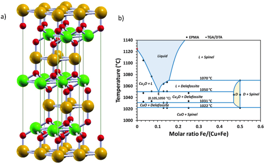 | ||
| Fig. 13 (a) Delafossite ABO2 crystal structure. Atoms by colours: A (orange), B, (green), and oxygen (red). Reproduced unchanged from ref. 134 according to https://creativecommons.org/licenses/by/4.0/©2017 Informa UK Limited, trading as Taylor & Francis Group. (b) Experimental phase diagram of the Cu–Fe–O system in air, with experimental points with an accuracy of ± 2 °C for the transition temperatures. D = delafossite; L = eutectic CuFeO2 + Cu2O; spinel + CuFe2O4 + Fe3O4. Reprinted (adapted) with permission from ref. 138 Copyright 2019 American Chemical Society. | ||
CuFeO2 is an interesting candidate for PEC applications, particularly H2 generation, with appropriate absorption and band alignment with water reduction potential, as depicted in Fig. 2. The valence band is mainly composed of Cu 3d and O 2p orbitals, while the VB and CB edges are constituted by Cu and Fe 3d states, with a band gap energy in the order of ∼1.5 eV (but with variable values found in the literature).135 Additionally, CuFeO2 consisted of earth-abundant elements, with favourable stability (mainly in alkaline electrolytes) and relatively high conductivity, due to the high covalent character of the Cu–O bond when compared to typical metal–O bonds in other oxides.136
Although promising, the synthesis of pure CuFeO2 remains a challenge. The Cu–Fe–O system is highly influenced by temperature and Cu/Fe ratio and the CuFeO2 synthesis in high temperatures usually generates CuO, Fe2O3 and CuFeO4 as side products.137 In Fig. 13(b), we reproduce an experimental phase diagram built from thermogravimetric (TGA) and differential analysis (DTA) data in air, complemented by in situ XRD, and field-emission-gun electron probe microanalysis (EMPA) studies by Shorne-Pinto and co-workers.138 The delafossite temperature formation relies on the interval ranging from 1022 to 1070 °C, where decomposition starts, with the possible formation of non-stoichiometric forms that could compromise the PEC performance.
Pure phase CuFeO2 crystals are usually obtained under temperatures above 1000 °C, an inert atmosphere, or high vacuum. However, the synthesis of hexagonal crystallographic phase (P63/mmc), referred to as 2H-CuFeO2 can occur via low-temperature solution-based methods. Jin and Chumanov used high basic conditions at temperature <100 °C and obtained 2H-CuFeO2 nanoplates, 100 nm thick, with Eg of 1.33 eV for photovoltaic applications.139 HT can also be used for non-pure CuFeO2 synthesis, including for direct deposition on FTO, as described by Tu and Chang (in most conditions with Cu2O impurities) for application in the degradation of dyes.140
Several studies report the combination of “wet” methods followed by post-annealing treatments in temperatures lower than 800 °C. In 2015, Sivula and co-workers obtained nanoporous CuFeO2 films with ∼300 nm of thickness using a sol–gel method, further deposited on FTO using spin-coating, with subsequent heat and depositions, and a final treatment under 700 °C by 12 h.141 The effects of deposition of Pt particles, aluminum-doped ZnO and TiO2 overlayers (15 nm/100 nm) by atomic layer deposition, were also evaluated. These electrodes exhibited a photocurrent density of 0.4 mA cm−2 for water reduction at 0 V vs. RHE in 0.5 M Na2SO4 (pH 6.1). When the delafossite layers were intercalated with oxygen using a post annealing process at 300 °C, photocurrents of 1.51 mA cm−2 at 0.35 V vs. RHE were reached for the oxygen reduction reaction. Furthermore, bare CuFeO2 electrodes were highly stable at potentials where photocurrent is observed, without degradation for at least 40 h under operating conditions in oxygen-saturated electrolyte.
Other combinations of methods are also observed. Recently, Luo et al. previously synthesized bulk CuFeO2 by SSR combined with pressure-less synthesis, followed by a heteroepitaxial growth of 16 nm thick CuFeO2 films on sapphire substrates using PLD.142
In 2016, Jang and co-workers143 used a synthesis method based on direct spin coating deposition of copper and iron nitrate precursors on a FTO substrate on a hot plate (450 °C/1 H). After this step, the electrodes were annealed for 10 h under Ar flow, at 500, 600 or 700 °C, to transform amorphous copper iron oxide into a crystalline delafossite structure. Furthermore, the films were submitted to different post treatments (conventional annealing at 300 °C/1H, or microwave heating for 1 to 15 min). The PEC experiments were then conducted for the HER at 0.4 V vs. RHE in aqueous 1 mol L−1 NaOH. While the non-heated electrode exhibited a photocurrent of only −0.3 mA cm−2, conventional thermal annealing doubled the photocurrent to −0.62 mA cm−2. In its turn, the microwave heating enhanced the photocurrent about 4 times, ∼−1.3 m mA cm−2 at 0.4 V vs. RHE. They claim that thermal treatment works by intercalating extra oxygen into the CuFeO2 lattice, which increases the charge carrier density, improving charge transport properties. They also conclude that when the annealing is made via microwave, the oxygen intercalation occurs more uniformly over the whole solid, being more effective.
However, as observed by Lumley et al. the microwave treatment can cause significant changes in the delafossite structure, since Cu1+ ions can be easily oxidized to Cu2+; then, CuO can be produced when CuFeO2 is heated in the air, influencing the PEC electrode performance.7 Thus, any air treatment of Cu1+ ternary oxides should be carefully investigated to assure that the enhancement in photocurrent is only due to changes in the bulk lattice of the original compound and not to the formation of some CuO.
Furthermore, Mg2+ can substitute Fe3+ in the delafossite lattice, serving as a p-type donor and increasing carrier concentration and photoinduced carrier lifetime. However, Wuttig et al. highlighted that the majority carrier can change from p-type to n-type near the Mg solubility limit (x = 0.05) in CuFeO2.144 In addition to doping, other strategies to enhance CuFeO2 properties, include a heterojunction with other materials, especially with CuO, performed using several of the above discussed methods.145–148
To sum up, CuFeO2 is a promising semiconductor for application as a photocathode for water splitting and the CO2RR, with a lower band gap and higher stability in relation to its binary counterpart Cu2O.147,148 However, the experimentally obtained PEC performance is lower than the theoretical estimated values (photovoltage of 0.8 V and photocurrent of ∼9 mA cm−2),137,148,149 due to poor photoinduced electron–hole separation and collection. Thus, efforts for building adequate heterostructures using a combination of different synthesis methods can suppress surface and bulk recombination and improve the PEC performance of CuFeO2.149
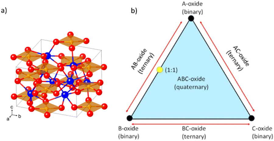 | ||
| Fig. 14 (a) The CuBi2O4 crystal structure as viewed at an arbitrary angle. The Bi, Cu, and O atoms are represented by blue, orange, and red spheres, respectively. Reprinted (adapted) with permission from ref. 16 Copyright 2016 American Chemical Society. (b) Graphical visualization of ternary and quaternary oxides, for generic cases. Adapted from ref. 155 according to (CC BY, https://creativecommons.org/licenses/by/4.0/)©The Author(s) 2018. Published by ECS. | ||
CuBi2O4 behaves as a p-type semiconductor and has been considered a promising photocathode for PEC, especially water splitting, since 2007,14,151,152 due to the narrow optical bandgap (Eg ranging from 1.5 to 1.8 eV), VB edge located at a more positive potential than Cu2O and CuFeO2 (with a photocurrent onset potential near 1 V vs. RHE) and CB edge more negative than the thermodynamic reduction potential of H+/H2 (0 V vs. RHE).133 Recently, a CuBi2O4 photoelectrode was also investigated for the CO2RR in 0.1 mol L−1 KHCO3 aqueous solution (pH = 6.8, CO2 saturated), and produced CO at 0 V vs. Ag/AgCl. Also, ethanol and formaldehyde were produced using a photoelectrode consisting of a composite of CuBi2O4 with TiO2 nanotubes in 0.1 M NaHCO3 solution and −0.6 V vs. SCE.153,154
CuBi2O4 can be synthesized from a combination of CuO and Bi2O3 in a 1:1 stoichiometry.155 This can be visualized in a scheme in Fig. 14(b), which brings a diagram of different combinations of binary oxide precursors and the resulting complex multinary oxides. Considering A as CuO and B as Bi2O3, the yellow dot on the triangle edge middle would be the stoichiometric compound CuBi2O4. The addition of another C oxide, such as V2O5, could result in a quaternary oxide.
As for other complex oxides, conventional “dry” methods like SSR, are commonly employed for CuBi2O4 preparation. However, the reaction begins at temperatures over 600 °C, and CuBi2O4 melts over ∼820 °C.152,156 Ball milling can be employed in combination to SSR, like in the work of Wei and co-workers, who prepared a p–n heterojunction photocatalyst of p-CuBi2O4/n-TiO2,157 but, according to Chen et al., it must be carefully employed in the CuBi2O4 synthesis, as it can causes structural modifications.158
Conventional “wet” methods have also been used for CuBi2O4 synthesis, although the occurrence of non-stoichiometry,159 and presence of CuO and Bi2O3 impurities is expected at lower temperatures (∼200 °C).156 The CuBi2O4 preparation by electrodeposition,159 hydrothermal,160,161 and sol–gel methods,162 usually must be followed by heating treatments and the resulting electrodes give highly negative photoelectrochemical currents, like −1.5 mA cm−2 at 0.45 V vs. Ag/AgCl for HER, and −0.1 mA cm−2 at 0 V vs. Ag/AgCl for CO2RR into CO.160,163–165
Li et al.166 reported the effect of the annealing conditions of CuBi2O4 directly synthesized on FTO via spin-coating of Cu and Bi nitrate solutions, with a hot plate (120 °C) and post-annealing over 450 °C in a furnace for 2 h. For comparison purposes, four different ramping rates were set (1 °C min−1, 2 °C min−1, 10 °C min−1 and 20 °C min−1). The CuBi2O4 electrode slowly heated at 2 °C min−1 up to 450 °C achieved the highest photocurrent, 0.68 mA cm−2 at 0.25 VRHE in KOH/KCl electrolyte, pH 13.
Unconventional methods were also used for CuBi2O4 preparation; in 2017, Hossain et al. reported successful CuBi2O4 preparation via combustion solution synthesis; however, the samples also presented different quantities of residual CuO and BiO3.167 The studies revealed that the electrode prepared with CuO/CuBi2O4 heterojunction, showed improved photocurrent in comparison with electrodes prepared with these oxides alone, which they attributed to a synergic effect of enhanced charge carrier separation in the nanocomposite. More recently, Gottesman et al. prepared high-crystalline and pure phase CuBi2O4 electrodes by the subsequential deposition of BiO3 and CuO layers on FTO substrate with PLD at a substrate temperature at 500 °C, followed by a floating zone technique for crystal growth, and a rapid thermal process at 650 °C for 10 min.168 In another study, a film of CuBi2O4 was directly deposited on FTO by PLD.156 In both studies they observed higher photocurrents for samples with impurities, compared to the pure ones. The authors warned that conventional long furnace annealing, e.g. 500 °C for 72 h, can result in uncontrolled phase segregation and such impurities prevent the synthesis of pure phase CuBi2O4.156 Thus, they advertised the importance of searching for pure phases to control PEC performance.
Lee and co-workers used PLD to prepare high-quality single crystal CuBi2O4 thin film using a NiO template layer grown on (001) SrTiO3 single-crystal substrate.169 Since PLD can be implicated in epitaxial relationships among the domains of each component, the substrate was carefully selected to guarantee the maximum compatibility and minimum tension of film/substrate crystal lattice parameters.170 The resulting photocathode exhibits −0.4 mA cm−2 at 0 V RHE under illumination in 0.1 mol L−1 potassium phosphate solution; the addition of H2O2 as an electron scavenger intensified the photocurrent to −0.7 mA cm−2.
The experimental performances reported for CuBi2O4 photoelectrodes are lower than its maximum theoretical photocurrent calculated as ∼20 mA cm−2 assuming 100% of absorption and conversion for photons with an energy above its Eg of 1.8 eV. According to Berglund et al., the CuBi2O4 main limiting factor for PEC performance is the poor charge carrier transport (primarily by holes), combined with its relatively weak optical absorption and instability in aqueous media.16
The strategies to circumvent these problems include, again, the nanostructuring, doping, surface modifications and also the use of protective layers.171 Moreover, suitable contact between CuBi2O4 and the conductive substrate must be assured. Furthermore, FTO is largely used as a substrate, but it should also be pointed out that there is a mismatch between the FTO work function and the CuBi2O4 Fermi level, which can create a Schottky barrier, prejudicing the hole transport.172 In this sense, it is also important to optimize the substrate and intermediate layers associated with the efforts for more adequate synthesis methods.
Fig. 15 shows a timeline for the evolution of CuBi2O4 synthesis methods, which includes the main discussed synthesis methods for the preparation of CuBi2O4 based photocathodes.
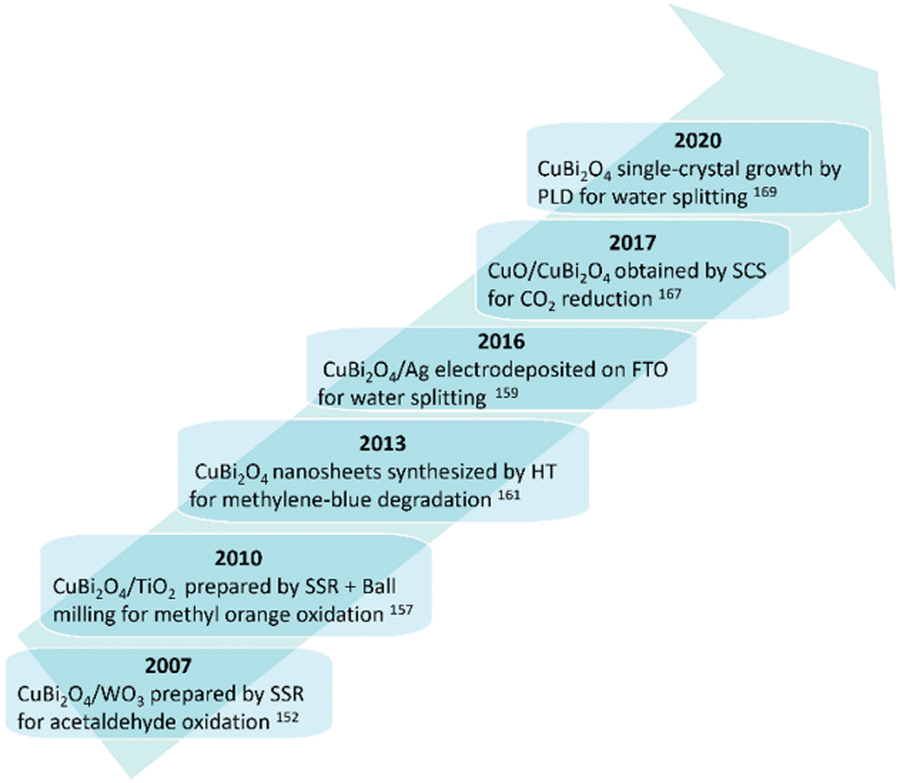 | ||
| Fig. 15 General timeline for the evolution of some reports in the literature of CuBi2O4 electrodes for PEC applications obtained by conventional “dry methods” (solid-state reaction, ball-milling) or “wet methods” (hydrothermal, electrodeposition) and by less conventional methods such as solution combustion synthesis and pulsed-laser deposition. | ||
5. Conclusions
In summary, the generation of fuels based on PEC water splitting, CO2 reduction or biomass valorisation using semiconductor electrodes are promising green technologies, but their real application depends on the efficiency and long-term stability of the materials used as photoelectrodes. Complex metal oxides with semiconductor properties can be the next generation materials for such PEC applications, due to the improved sunlight harvesting and enhanced stability in comparison to their binary counterparts. Moreover, the high number of possible combinations of metals (mainly the transition ones), can lead to novel (or little explored) complex oxides.However, the performances of these innovative materials as photoelectrodes in PEC reactors are still much lower than the maximum theoretical photocurrent calculated from their Eg values. Although complex oxides generally present interesting intrinsic properties, there are several kinetics and charge-transfer limitations, which must be circumvented to produce efficient photoelectrodes for PEC generation of fuels.
Comparison of PEC performances is not straightforward, since experimental conditions include numerous variables, such as electrode geometrical and electrochemical area, irradiation intensity, scavenger species, pH and electrolyte composition. However, photocurrent or faradaic efficiencies values have been presented here when these data were available.
The properties of complex oxides (as well as, for any material) can be improved by nanostructuring, doping, and/or with suitable heterojunctions. Since these strategies are synthesis-dependent, the choice of a reliable synthesis methodology is essential to develop multinary complex oxides which exhibit adequate characteristics for PEC applications.
The literature presents several methods to synthesize multinary oxides and the choice should consider advantages and disadvantages in terms of necessary facilities (precursors and equipment), and control of product characteristics (purity, crystallinity, morphology, thickness, and electrical contact with the substrate). While “dry” methods can easily produce crystalline complex oxides, “wet” methods are more favourable to control the morphology and grain size. Furthermore, a combination of different methods can be a good strategy to balance morphological and crystallinity aspects. However, an annealing step is usually necessary for the preparation of photoelectrodes with samples obtained from both routes. Moreover, the direct growth of complex oxide films on the conductive substrate by electrodeposition, CVD or PVD bring enhanced properties in terms of adherence and electrical contact, the required properties for photoelectrodes. Nevertheless, these methodologies are not trivial and cannot be largely applied for complex oxide synthesis.
Far from being an instructions guide, this work was an attempt to bring insights into the choice of a methodology to synthesize complex oxides for PEC applications, organized as “traditional” (widely used methods), and “unconventional” methods. This way, we hope to contribute to the development of more efficient materials for the next generation production of solar fuels, such as hydrogen from water splitting, C-based products from CO2 or biomass valorisation and other reactions in the field of sustainable energy production.
Author contributions
All authors participated into the conceptualization of this work. CRediT: N. G. Macedo: methodology, writing – original draft (Introduction, “Wet” and Unconventional Methods, Photocathodes, Conclusion sections), writing – review & editing; J. C. A., L. C. S. & M. T. G.: writing – original draft (Fundamentals, “Wet” and Unconventional Methods); L. S.C. & L. C. S.: writing – original draft (“Dry” methods and Photoanodes); V. S. L.: writing – original draft (“Wet” and Photocathodes). C. Longo: supervision, resources, validation, writing-review & editing. All authors approve the content of the manuscript and agree to be held accountable for the work.Conflicts of interest
There are no conflicts to declare.Acknowledgements
The authors gratefully acknowledge the financial support from the Coordination of Superior Level Staff Improvement (CAPES) Process 88881.310535/2018-01, Finance Code 001, the National Council for Scientific and Technological Development (CNPq) Processes 131552/2020-1, 306948/2021-4 and 150861/2022-2, the Center for Innovation on New Energies (CINE) and São Paulo Research Foundation (FAPESP) Processes 2017/11986-5, 2019/09838-3 and 2021/05853-8, as well as Shell and the strategic importance of the support given by ANP (Brazil's National Oil, Natural Gas and Biofuels Agency) through the R&D levy regulation.Notes and references
- J. R. Galan-Mascaros, Catal. Sci. Technol., 2020, 10, 1967 RSC.
- L. M. Peter, in Photoelectrochemical Solar Fuel Production: From Basic Principles to Advanced Devices, ed. S. Giménez and J. Bisquert, Springer Cham, 2016, ch. 1, vol. 1, pp. 3–40 Search PubMed.
- J. H. Kim, D. Hansora, P. Sharma, J.-W. Jang and J. S. Lee, Chem. Soc. Rev., 2019, 48, 1908 RSC.
- J. L. White, M. F. Baruch, J. E. Pander III, Y. Hu, I. C. Fortmeyer, J. E. Park, T. Zhang, K. Liao, J. Gu, Y. Yan, T. W. Shaw, E. Abelev and A. B. Bocarsly, Chem. Rev., 2015, 115, 12888 CrossRef CAS PubMed.
- J. H. Montoya, L. C. Seitz, P. Chakthranont, A. Vojvodic, T. F. Jaramillo and J. K. Nørskov, Nat. Mater., 2017, 16, 70 CrossRef PubMed.
- A. Dey, F. A. Houle, C. E. Lubner, M. Sevilla and W. J. Shaw, Chem. Commun., 2021, 57, 1540 RSC.
- M. A. Lumley, A. Radmilovic, Y. J. Jang, A. E. Lindberg and K.-S. Choi, J. Am. Chem. Soc., 2019, 141, 18358 CrossRef CAS PubMed.
- J. Wang, T. van Ree, Y. Wu, P. Zhang and L. Gao, in Metal Oxides Series, Metal Oxides in Energy Technologies, ed. Y. Wu, Elsevier, 2018, ch. 8, pp. 205–249 Search PubMed.
- C. Li, Z. Luo, T. Wang and J. Gong, Adv. Mater., 2018, 30, e1707502 CrossRef PubMed.
- S. O’Donnell, A. Vali, A. Rawat, P. A. Maggard, M. N. Huda and K. Rajeshwar, ECS J. Solid State Sci. Technol., 2022, 11, 053001 CrossRef.
- M. Ma, Y. Huang, J. Liu, K. Liu, Z. Wang, C. Zhao, S. Qu and Z. Wang, J. Semicond., 2020, 41, 091702 CrossRef CAS.
- I. V. Bagal, N. R. Chodankar, M. A. Hassan, A. Waseem, M. A. Johar, D.-H. Kim and S.-W. Ryu, Int. J. Hydrogen Energy, 2019, 44, 21351 CrossRef CAS.
- M. T. Galante, P. Sotelo, M. K. Hossain, A. Vali, A. Raamann, C. Longo, R. T. Macaluso and K. Rajeshwar, Chem. Electro Chem., 2019, 6, 87 CAS.
- F. F. Abdi and S. P. Berglund, J. Phys. D: Appl. Phys., 2017, 50, 193002 CrossRef.
- M. Woodhouse and B. A. Parkinson, Chem. Soc. Rev., 2009, 38, 197 RSC.
- S. P. Berglund, F. F. Abdi, P. Bogdanoff, A. Chemseddine, D. Friedrich and R. vand de Krol, Chem. Mater., 2016, 28, 4231 CrossRef CAS.
- A. Arimi, L. Megatif, L. I. Granone, R. Dillert and D. W. Bahnemann, J. Photochem. Photobiol., A, 2018, 366, 118 CrossRef CAS.
- J. Li and N. Wu, Catal. Sci. Technol., 2015, 5, 1360 RSC.
- S. Omeiri, B. Bellal, A. Bouguelia, Y. Bessekhouad and M. Trari, J. Solid State Electrochem., 2008, 13, 1395 CrossRef.
- E. Kalamaras, M. M. Maroto-Valer, M. Shao, J. Xuan and H. Wang, Catal. Today, 2018, 317, 56 CrossRef CAS.
- C. Y. Toe, Z. Zheng, H. Wu, J. Scott, R. Amal and Y. H. Ng, Angew. Chem., Int. Ed., 2018, 57, 13613 CrossRef CAS PubMed.
- S. Chen, D. Huang, P. Xu, W. Xue, L. Lei, M. Cheng, R. Wang, X. Liu and R. Deng, J. Mater. Chem. A, 2020, 8, 2286 RSC.
- T. S. Bui, E. C. Lovell, R. Daiyan and R. Amal, Adv. Mater., 2023, 35, 2205814 CrossRef CAS PubMed.
- A. Eftekhari, V. J. Babu and S. Ramakrishna, Int. J. Hydrogen Energy, 2017, 42, 11078 CrossRef CAS.
- C. N. R. Rao, Mater. Sci. Eng., B, 1993, 18, 1 CrossRef.
- L. Cruz, M. M. Teixeira, V. Teodoro, N. Jacomaci, L. O. Laier, M. Assis, N. G. Macedo, A. C. M. Tello, L. F. da Silva, G. E. Marques, M. A. Zaghete, M. D. Teodoro and E. Longo, CrystEngComm, 2020, 22, 7903 RSC.
- R. Merkle and J. Maier, Angew. Chem., Int. Ed., 2008, 47, 3874 CrossRef CAS PubMed.
- F. Moosakazemi, M. R. Tavakoli Mohammadi, M. Mohseni, M. Karamoozian and M. Zakeri, Int. J. Miner. Process., 2017, 165, 41 CrossRef CAS.
- G. Kaupp, CrystEngComm, 2009, 11, 388 RSC.
- T. Wang, J. Liu, W. Jiang, F. Jiang, G. Feng, L. Miao, Q. Zhang, Q. Wu and X. Lao, Ceram. Int., 2022, 48, 24044 CrossRef CAS.
- F. Saib, F. Özel, A. Sarılmaz, O. Mahroua, B. Bellal and M. Trari, Mater. Sci. Semicond. Process., 2019, 91, 174 CrossRef CAS.
- A. Priya, P. Arunachalam, A. Selvi, J. Madhavan, A. M. Al-Mayouf and M. A. Ghanem, Opt. Mater., 2018, 81, 84 CrossRef CAS.
- Y. Zhou, Phys. Sci. Rev., 2020, 5, 20180084 Search PubMed.
- B. B. Lakshmi, P. K. Dorhout and C. R. Martin, Chem. Mater., 1997, 9, 857 CrossRef CAS.
- A. E. Danks, S. R. Hall and Z. Schnepp, Mater. Horiz., 2016, 3, 91 RSC.
- S. Esposito, Materials, 2019, 12, 668 CrossRef CAS PubMed.
- M. Parashar, V. K. Shukla and R. Singh, J. Mater. Sci.: Mater. Electron., 2020, 31, 3729 CrossRef CAS.
- A. C. Pierre, Introduction to Sol–Gel Processing, Springer, Cham, 2020 Search PubMed.
- A. Styskalik, D. Skoda, C. E. Barnes and J. Pinkas, Catalysts, 2017, 7, 168 CrossRef.
- M. S. Sheikh, D. Ghosh, T. K. Bhowmik, A. Dutta, S. Bhattacharyya and T. P. Sinha, Mater. Chem. Phys., 2020, 244, 122685 CrossRef CAS.
- X. Liang, J. Xie, J. Xiong, L. Gong and C. M. Li, Sustainable Energy Fuels, 2018, 2, 2053 RSC.
- K. Byrappa and T. Adschiri, Prog. Cryst. Growth Charact. Mater., 2007, 53, 117 CrossRef CAS.
- S. H. Feng and G. H. Li, in Modern Inorganic Synthetic Chemistry, ed. R. Xu and Y. Xu, Elsevier, Amsterdam, 2017, ch. 4, vol. 2, pp. 73–104 Search PubMed.
- B. G. Rao, D. Mukherjee and B. M. Reddy, in Nanostructures for Novel Therapy: Synthesis, Characterization, and Applications, ed. D. Ficai and A. M. Grumezescu, Elsevier, 2017, ch. 1, pp. 1–36 Search PubMed.
- X. Wu, C. Y. Toe, C. Su, Y. H. Ng, R. Amal and J. Scott, J. Mater. Chem. A, 2020, 8, 15302 RSC.
- X. Wang, Z. Liu and Z. Liu, ChemCatChem, 2017, 9, 4029 CrossRef CAS.
- D. A. Keller, H.-N. Barad, E. Rosh-Hodesh, A. Zaban and D. Cahen, MRS Commun., 2018, 8, 1358 CrossRef CAS.
- Th. Pauporté, A. Goux, A. Kahn-Harari, N. de Tacconi, C. R. Chenthamarakshan, K. Rajeshwar and D. Lincot, J. Phys. Chem. Solids, 2003, 64, 1737 CrossRef.
- G. V. Govindaraju, G. P. Wheeler, D. Lee and K.-S. Choi, Chem. Mater., 2017, 29, 355 CrossRef CAS.
- T. M. David, P. R. Dev, P. Wilson, P. Sagayaraj and T. Mathews, Electrochem. Sci. Adv., 2022, 2, e202100083 CrossRef CAS.
- N. Alias, S. A. Rosli, N. Bashirom, M. Rozana, W. K. Tan, G. Kawamura, P. Nbelayim, A. Matsuda, Z. Hussain and Z. Lockman, in Micro and Nano Technologies, Nanostructured Anodic Metal Oxides, ed. G. D. Sulka, Elsevier, 2020, ch. 8, pp. 277–303 Search PubMed.
- R. Akbari, G. Godeau, M. Mohammadizadeh, F. Guittard and T. Darmanin, Appl. Surf. Sci., 2020, 503, 144094 CrossRef CAS.
- F. Bouhjar, L. Derbali, B. Marí and B. Bessaïs, Int. J. Hydrogen Energy, 2020, 45, 11492 CrossRef CAS.
- Y. Makimizu, N. T. Nguyen, J. Tucek, H.-J. Ahn, J. Yoo, M. Poornajar, I. Hwang, S. Kment and P. Schmuki, Chem. – Eur. J., 2020, 26, 2685 CrossRef CAS PubMed.
- N. Labchir, A. Hannour, D. Vincent, A. A. Hssi, M. Ouafi, K. Abouabassi, A. Ihlal and M. Sajieddine, J. Electron. Mater., 2020, 49, 2242 CrossRef CAS.
- M. C. Rao, Int. J. Mod. Phys.: Conf. Ser., 2013, 22, 355 CAS.
- H. M. Smith and A. F. Turner, Appl. Opt., 1965, 4, 147 CrossRef.
- D. Dijkkamp, T. Venkatesan, X. D. Wu, S. A. Shaheen, N. Jisrawi, Y. H. Min-Lee, W. L. McLean and M. Croft, Appl. Phys. Lett., 1987, 51, 619 CrossRef CAS.
- H.-U. Krebs, M. Weisheit, J. Faupel, E. Süske, T. Scharf, C. Fuhse, M. Störmer, K. Sturm, M. Seibt, H. Kijewski, D. Nelke, E. Panchenko and M. Buback, in Advances in Solid State Physics, ed. B. Kramer, Springer, Berlin, Heildelberg, 2003, pp. 505–518 Search PubMed.
- K. Park, Y. J. Kim, T. Yoon, S. David and Y. M. Song, RSC Adv., 2019, 9, 30112 RSC.
- A. V. Rane, K. Kanny, V. K. Abitha and S. Thomas, in Micro and Nano Technologies, ed. S. M. Bhagyaraj, O. S. Oluwafemi, N. Kalarikkal and S. Thomas, Woodhead Publishing, 2018, ch. 5, pp. 121–139 Search PubMed.
- I. Ohkubo, Y. Matsumoto, K. Ueno, T. Chikyow, M. Kawasaki and H. Koinuma, J. Cryst. Growth, 2003, 247, 105 CrossRef CAS.
- E. M. Preiß, T. Rogge, A. Krauß and H. Seidel, Sens. Actuators, B, 2016, 236, 865 CrossRef.
- R. D. Gretz, C. M. Jackson and J. P. Hirth, Surf. Sci., 1967, 6, 171 CrossRef CAS.
- B. Silva, J. Rodrigues, B. Sompalle, C.-D. Liao, N. Nicoara, J. Borme, F. Cerqueira, M. Claro, S. Sadewasser, P. Alpuim and A. Capasso, Nanomaterials, 2021, 11, 1650 CrossRef CAS PubMed.
- H. O. Pierson, Handbook of Chemical Vapor Deposition: Principles, Technology and Applications, Willian Andrew, Elsevier, 1999 Search PubMed.
- Y. Xu and X.-T. Yan, Chemical Vapours Deposition: An Integrated Engineering Design for Advanced Materials. Springer, London, 2010 Search PubMed.
- F. E. Annanouch, S. Vallejos, T. Stoycheva, C. Blackman and E. Llobet, Thin Solid Films, 2013, 548, 703 CrossRef CAS.
- A. Kay, I. Cesar and M. Grätzel, J. Am. Chem. Soc., 2006, 128, 15714 CrossRef CAS PubMed.
- D. Bekermann, D. Barreca, A. Gasparotto and C. Maccato, CrystEngComm, 2012, 14, 6347 RSC.
- T. Wang, Z. Luo, C. Li and J. Gong, Chem. Soc. Rev., 2014, 43, 7469 RSC.
- A. Paracchino, V. Laporte, K. Sivula, M. Grätzel and E. Thimsen, Nat. Mater., 2011, 10, 456 CrossRef CAS PubMed.
- A. Paracchino, N. Mathews, T. Hisatomi, M. Stefik, S. D. Tilley and M. Grätzel, Energy Environ. Sci., 2012, 5, 8673 RSC.
- L. F. da Silva, W. Avansi, J. Andres, C. Ribeiro, M. L. Moreira, E. Longo and V. R. Mastelaro, Phys. Chem. Chem. Phys., 2013, 15, 12386 RSC.
- J. Zhao, S. Ge, D. Pan, Y. Pan, V. Murugadoss, R. Li, W. Xie, Y. Lu, T. Wu, E. K. Wujcik, Q. Shao, X. Mai and Z. Guo, J. Electrochem. Soc., 2019, 166, H3074 CrossRef CAS.
- Y. Hou, C. Zheng, Z. Zhu and X. Wang, Chem. Commun., 2016, 52, 6888 RSC.
- E. Carlos, R. Martins, E. Fortunato and R. Branquinho, Chem. – Eur. J., 2020, 26, 9099 CrossRef CAS PubMed.
- F. Siddique, S. Gonzalez-Cortes, A. Mirzaei, T. Xiao, M. A. Rafiq and X. Zhang, Nanoscale, 2022, 14, 11806 RSC.
- P. Ravindranathan and K. C. Patil, J. Mater. Sci. Lett., 1986, 5, 221 CrossRef CAS.
- M. K. Hossain, P. Sotelo, H. P. Sarker, M. T. Galante, A. Kormányos, C. Longo, R. T. Macaluso, M. N. Huda, C. Janáky and K. Rajeshwar, ACS Appl. Energy Mater., 2019, 2, 2837 CrossRef CAS.
- K. Deshpande, A. Mukasyan and A. Varma, Chem. Matter, 2004, 16, 4896 CrossRef CAS.
- K. C. Patil, M. S. Hegde, T. Rattan and S. T. Aruna, Chemistry of Nanocrystalline Oxide Materials, World Scientific, 2008 Search PubMed.
- A. Varma, A. S. Mukasyan, A. S. Rogachev and K. V. Manukyan, Chem. Rev., 2016, 116, 14493 CrossRef CAS PubMed.
- F.-T. Li, J. Ran, M. Jaroniec and S. Z. Qiao, Nanoscale, 2015, 7, 17590 RSC.
- T. Tatarchuk, A. Shyichuk, J. Lamkiewicz and J. Kowalik, Ceram. Int., 2020, 46, 14674 CrossRef CAS.
- S. V. Bhandare, R. Kumar, A. V. Anupama, H. K. Choudhary, V. M. Jali and B. Sahoo, Ceram. Int., 2020, 46, 17400 CrossRef CAS.
- P. Heidari and S. M. Masoudpanah, J. Alloys Compd., 2020, 834, 155166 CrossRef CAS.
- G. Takalkar, R. R. Bhosale, F. AlMomani, A. Kumar, A. Banu, A. Ashok, S. Rashid, M. Khraisheh, A. Shakoor and A. al Ashraf, Appl. Surf. Sci., 2020, 509, 144908 CrossRef CAS.
- A. Varga, G. F. Samu and C. Janáky, Electrochim. Acta, 2018, 272, 22 CrossRef CAS.
- A. Kormányos, A. Thomas, M. N. Huda, P. Sarker, J. P. Liu, N. Poudyal, C. Janáky and K. Rajeshwar, J. Phys. Chem. C, 2016, 120, 16024 CrossRef.
- M. R. da Silva Pelissari, L. V. A. Scalvi, V. S. L. Neto and L. H. Dall’Antonia, J. Mater. Sci.: Mater. Electron., 2020, 31, 2833 CrossRef CAS.
- M. K. Hossain, H. P. Sarker, P. Sotelo, U. Dang, I. Rodríguez-Gutiérrez, J. Blawat, A. Vali, W. Xie, G. Oskam, M. N. Huda, R. T. Macaluso and K. Rajeshwar, Chem. Mater., 2020, 32, 6247 CrossRef CAS.
- X. Zhang, W. Jiang, D. Song, H. Sun, Z. Sun and F. Li, J. Alloys Compd., 2009, 475, L34 CrossRef CAS.
- M. K. Hossain, E. Kecsenovity, A. Varga, M. Molnár, C. Janáky and R. Rajeshwar, Int. J. Self-Propag. High-Temp. Synth., 2018, 27, 129 CrossRef CAS.
- J. Yu, Y. Ni and M. Zhai, J. Phys. Chem. Solids, 2018, 112, 119 CrossRef CAS.
- N. S. Sarvestani, M. H. Abbaspour-Fard, M. Tabasizadeh, H. Nayebzadeh, T. C. Van, M. Jafari, Z. Ristovski and R. J. Brown, J. Alloys Compd., 2020, 838, 155627 CrossRef CAS.
- A. Hezam, K. Namratha, Q. A. Drmosh, D. Ponnamma, J. Wang, S. Prasad, M. Ahamed, C. Cheng and K. Byrappa, ACS Appl. Nano Mater., 2020, 3, 138 CrossRef CAS.
- H.-Y. Mu, F.-T. Li, X.-T. An, R.-H. Liu, Y.-L. Li, X. Qian and Y.-Q. Hu, Phys. Chem. Chem. Phys., 2017, 19, 9392 RSC.
- R. García, G. A. Hirata and J. McKittrick, J. Mater. Res., 2011, 16, 1059 CrossRef.
- T. S. Cam, T. A. Vishnevskaya, S. O. Omarov, V. N. Nevedomskiy and V. I. Popkov, J. Mater. Sci., 2020, 55, 11891 CrossRef CAS.
- S. Meena, L. Renuka, K. S. Anantharaju, Y. S. Vidya, H. P. Nagaswarupa, S. C. Prashantha and H. Nagabhushana, Mater. Today: Proc., 2017, 4, 11773 Search PubMed.
- H. L. Tan, R. Amal and Y. H. Ng, J. Mater. Chem. A, 2017, 5, 16498 RSC.
- P. Mane, I. V. Bagal, H. Bae, A. N. Kadam, V. Burungale, J. Heo, S.-W. Ryu and J. S. Ha, Int. J. Hydrogen Energy, 2022, 47, 39796 CrossRef CAS.
- J. Chi, Z. Jiang, J. Yan, A. Larimi, Z. Wang, L. Wang and W. Shangguan, Mater. Today, 2022, 26, 101060 CAS.
- H. Shi, H. Guo, S. Wang, G. Zhang, Y. Hu, W. Jiang and G. Liu, Energy Fuels, 2022, 36, 1404 Search PubMed.
- J. A. Seabold and K. S. Choi, J. Am. Chem. Soc., 2012, 134, 2186 CrossRef CAS PubMed.
- N. A. Mohamed, N. A. Arzaee, M. F. M. Noh, A. F. Ismail, J. Safaei, J. S. Sagu, M. R. Johan and M. A. M. Teridi, Ceram. Int., 2021, 47, 24227 CrossRef CAS.
- K. J. McDonald and K.-S. Choi, Energy Environ. Sci., 2012, 5, 8553 RSC.
- D. K. Lee and K.-S. Choi, Nat. Energy, 2018, 3, 53 CrossRef CAS.
- K. R. Tolod, S. Hernández, M. Castellino, F. A. Deorsola, E. Davarpanah and N. Russo, Int. J. Hydrogen Energy, 2020, 45, 605 CrossRef CAS.
- S. N. H. Yassin, A. S. L. Sim and J. R. Jennings, Nano Mater. Sci., 2020, 2, 227 CrossRef.
- C. Seong, P. Mane, H. Bae, S. Lee, S. H. Kang, S.-W. Ryu and J.-S. Ha, J. Electrochem. Soc., 2022, 169, 016501 CrossRef CAS.
- M. F. R. Samsudin, R. Bashiri, N. M. Mohamed, Y. H. Ng and S. Sufian, Appl. Surf. Sci., 2020, 504, 144417 CrossRef CAS.
- S. Hilliard, D. Friedrich, S. Kressman, H. Strub, V. Artero and C. Laberty-Robert, ChemPhotoChem, 2017, 1, 273 CrossRef CAS.
- S. G. Shim, J. Tan, H. Lee, J. Park, J. Yun, Y. S. Park, K. Kim, J. Lee and J. Moon, Chem. Eng. J., 2022, 430, 133061 CrossRef CAS.
- Y. Kuang, Q. Jia, G. Ma, T. Hisatomi, T. Minegishi, H. Nishiyama, M. Nakabayashi, N. Shibata, T. Yamada, A. Kudo and K. Domen, Nat. Energy, 2017, 2, 16191 CrossRef CAS.
- M. Kölbach, K. Harbauer, K. Ellmer and R. van de Krol, J. Phys. Chem. C, 2020, 124, 4438 CrossRef.
- X. Y. Meng, D. Y. Liu and G. W. Qin, Energy Environ. Sci., 2018, 11, 692 RSC.
- Q. Wang and K. Domen, Chem. Rev., 2020, 120, 919 CrossRef CAS PubMed.
- J. Kim, A. Ho-Baillie and S. Huang, Sol. RRL, 2019, 3, 1800302 CrossRef.
- J. H. Kim, J. H. Kim, J. H. Kim, Y. K. Kim and J. S. Lee, Sol. RRL, 2019, 4, 1900328 CrossRef.
- L. G. J. de Haart and G. Blasse, Solid State Ionics, 1985, 16, 137 CrossRef CAS.
- A. A. Tahir and K. G. U. Wijayantha, J. Photochem. Photobiol., A, 2010, 216, 119 CrossRef CAS.
- B. Joshi, E. Samuel, C. Park, Y. Kim, H.-S. Lee and S. A. Yoon, Appl. Surf. Sci., 2021, 559, 149951 CrossRef CAS.
- J. H. Kim, Y. J. Jang, S. H. Choi, B. J. Lee, M. H. Lee and J. S. Lee, ACS Sustainable Chem. Eng., 2019, 7, 944 CrossRef CAS.
- G. M. Morishita, I. R.-Gutiérrez, R. H. R. Castro and F. L. Souza, Mater. Lett., 2023, 340, 134176 CrossRef CAS.
- A. B. Silva, C. D. F. da Silva, F. L. Souza, F. W. S. Lucas and F. H. B. Lima, J. Catal., 2020, 391, 273 CrossRef CAS.
- N. Guijarro, P. Bornoz, M. Prévot, X. Yu, X. Zhu, M. Johnson, X. Jeanbourquin, F. Le Formal and K. Sivula, Sustainable Energy Fuels, 2018, 2, 103 RSC.
- W. Yang, R. R. Prabhakar, J. Tan, S. D. Tilley and J. Moon, Chem. Soc. Rev., 2019, 48, 4979 RSC.
- J. F. de Medeiros, M. T. Galante, R. Bertazzoli, C. G. P. dos Santos and C. Longo, ACS EST Water, 2022, 2, 982 CrossRef CAS.
- R. M. Arán-Ais, F. Scholten, S. Kunze, R. Rizo and B. Roldan Cuenya, Nat. Energy, 2020, 5, 317 CrossRef.
- M. T. Galante, A. Živković, J. C. Alvim, C. C. C. Kleiner, M. Sangali, S. F. R. Taylor, A. J. Greer, C. Hardacre, K. Rajeshwar, R. Caram, R. Bertazzoli, R. T. Macaluso, N. H. de Leeuw and C. Longo, ACS Appl. Mater. Interfaces, 2021, 13, 32865 CrossRef PubMed.
- J. K. Cooper, Z. Zhang, S. Roychoudhury, C.-M. Jiang, S. Gul, Y.-S. Liu, R. Dhall, A. Ceballos, J. Yano, D. Prendergast and S. E. R. Lillo, Chem. Mater., 2021, 33, 934 CrossRef CAS.
- R. Daou, R. Fresard, V. Eyert, S. Hébert and A. Maignan, Sci. Technol. Adv. Mater., 2017, 18, 919 CrossRef CAS PubMed.
- Q.-L. Liu, Z.-Y. Zhao, R.-D. Zhao and J.-H. Yi, J. Alloys Compd., 2020, 819, 153032 CrossRef CAS.
- H. Hiraga, T. Makino, T. Fukumura, H. Weng and M. Kawasaki, Phys. Rev. B: Condens. Matter Mater. Phys., 2011, 84, 041411(R) CrossRef.
- C. Li, J. He, Y. Xiao, Y. Li and J.-J. Delaunay, Energy Environ. Sci., 2020, 13, 3269 RSC.
- J. Schorne-Pinto, L. Cassayre, L. Presmanes and A. Barnabé, Inorg. Chem., 2019, 58, 6431 CrossRef CAS PubMed.
- Y. Jin and G. Chumanov, RSC Adv., 2016, 6, 26392 RSC.
- L.-W. Tu and K.-S. Chang, Mater. Chem. Phys., 2021, 267, 124620 CrossRef CAS.
- M. S. Prevot, N. Guijarro and K. Sivula, ChemSusChem, 2015, 8, 1359 CrossRef CAS PubMed.
- S. Luo, A. Fluri, S. Zhang, X. Liu, M. Döbeli, G. F. Harrington, R. Tu, D. Pergolesi, T. Ishihara and T. Lipeert, J. Appl. Phys., 2020, 127, 065301 CrossRef CAS.
- Y. Jang, Y. Park, H. E. Kim, Y. H. Choi, S. Choi and J. S. Lee, Chem. Mater., 2016, 28, 6054 CrossRef CAS.
- A. Wuttig, J. W. Krizan, J. Gu, J. J. Frick, R. J. Cava and A. B. Bocarsly, J. Mater. Chem. A, 2017, 5, 165 RSC.
- T. Jiang, Y. Zhao, M. Liu, Y. Chen, Z. Xia and H. Xue, Phys. Status Solidi A, 2018, 215, 1800056 CrossRef.
- T. Jiang, Y. Zhao and H. Xue, J. Mater. Sci., 2019, 54, 11951 CrossRef CAS.
- J. Yuan, L. Yang and C. Hao, Int. J. Electrochem. Sci., 2019, 14, 8569 CrossRef CAS.
- J. Gu, A. Wuttig, J. W. Krizan, Y. Hu, Z. M. Detweiler, R. J. Cava and A. B. Bocarsly, J. Phys. Chem. C, 2013, 117, 12415 CrossRef CAS.
- M. S. Prévot, X. A. Jeanbourquin, W. S. Bourée, F. Abdi, D. Friedrich, R. van de Krol, N. Guijarro, F. Le Formal and K. Sivula, Chem. Mater., 2017, 29, 4952 CrossRef.
- N. Henry, O. Mentre, J. C. Boivin and F. Abraham, Chem. Mater., 2001, 13, 543 CrossRef CAS.
- J. Li, M. Griep, Y. Choi and D. Chu, Chem. Commun., 2018, 54, 3331 RSC.
- T. Arai, M. Yanagida, Y. Konishi, Y. Iwasaki, H. Sugihara and K. Sayama, J. Phys. Chem. C, 2007, 111, 7574 CrossRef CAS.
- Y. Wang, H. Wang, A. R. Woldu, X. Zhang and T. He, Catal. Today, 2019, 335, 388 CrossRef CAS.
- H. Cao, H. Yu, Y. Lu, H. Zhang, G. Hou, Y. Tang and G. Zheng, ChemistrySelect, 2020, 5, 5137 CrossRef CAS.
- K. Rajeshwar, M. K. Hossain, R. T. Macaluso, C. Janáky, A. Varga and P. J. Kulesva, J. Electrochem. Soc., 2018, 165, H3192 CrossRef CAS.
- R. Gottesman, I. Levine, M. Schleuning, R. Irani, D. Abou-Ras, T. Dittrich, D. Friedrich and R. van de Krol, Adv. Energy Mater., 2021, 11, 2003474 CrossRef CAS.
- L. Wei, C. Shifu, Z. Sujuan, Z. Wei, Z. Huaye and Y. Xiaoling, J. Nanopart. Res., 2010, 12, 1355 CrossRef.
- X. L. Chen, J. K. Liang, Y. Liu, Y. C. Lan, Y. L. Zhang, Y. Ma, G. C. Che, G. D. Liu, X. Y. Xing and X. Y. Qiao, J. Appl. Phys., 1999, 85, 3155 CrossRef CAS.
- D. Kang, J. C. Hill, Y. Park and K.-S. Choi, Chem. Mater., 2016, 28, 4331 CrossRef CAS.
- L. Zhao, X. Wang and Z. Liu, Appl. Phys. A: Mater. Sci. Process., 2018, 124, 836 CrossRef.
- Y. Xie, Y. Zhang, G. Yang, C. Liu and J. Wang, Mater. Lett., 2013, 107, 291 CrossRef CAS.
- G. Seo, B. Kim, S. W. Hwang, S. S. Shin and I. S. Cho, Nano Energy, 2021, 80, 105568 CrossRef CAS.
- N. T. Hahn, V. C. Holmberg, B. A. Korgel and C. B. Mullins, J. Phys. Chem. C, 2012, 116, 6459 CrossRef CAS.
- N. Nasori, A. Rubiyanto and E. Endarko, J. Phys.: Conf. Ser., 2019, 1373, 12016 CrossRef CAS.
- D. Cao, N. Nasori, Z. Wang, Y. Mi, L. Wen, Y. Yang, S. Qu, Z. Wang and Y. Lei, J. Mater. Chem. A, 2016, 4, 8995 RSC.
- M. Li, X. Tian, X. Zou, X. Han, C. Du and B. Shan, Int. J. Hydrogen Energy, 2020, 45, 15121 CrossRef CAS.
- M. K. Hossain, G. F. Samu, K. Gandha, S. Santhanagopalan, J. P. Liu, C. Janáky and K. Rajeshwar, J. Phys. Chem. C, 2017, 121, 8252 CrossRef CAS.
- R. Gottesman, A. Song, I. Levine, M. Krause, A. T. M. N. Islam, D. Abous-Ras, T. Dittrich, R. van de Krol and A. Chemseddine, Adv. Funct. Mater., 2020, 30, 1910832 CrossRef CAS.
- J. Lee, H. Yoon, K. S. Choi, S. Kim, S. Seo, J. Song, B.-U. Choi, J. Ryu, S. Ryu, J. Oh, C. Jeon and S. Lee, Small, 2020, 16, 2002429 CrossRef CAS PubMed.
- J. Narayan and B. C. Larson, J. Appl. Phys., 2003, 93, 278 CrossRef CAS.
- Q. Zhang, B. Zhai, Z. Lin, X. Zhao and P. Diao, J. Phys. Chem. C, 2021, 125, 1890 CrossRef CAS.
- A. Song, P. Plate, A. Chemseddine, F. Wang, F. F. Absi, M. Wollgarten, R. van de Krol and S. P. Berglund, J. Mater. Chem. A, 2019, 7, 9183 RSC.
| This journal is © The Royal Society of Chemistry 2024 |