
 Open Access Article
 This Open Access Article is licensed under a Creative Commons Attribution-Non Commercial 3.0 Unported Licence
Borophene nanomaterials: synthesis and applications in biosensors
Gourang Hari
Gupta
,
Shikha
Kadakia
,
Darshan
Agiwal
,
Tanya
Keshari
and
Suveen
Kumar
 *
*
Department of Medical Devices, National Institute of Pharmaceutical Education and Research-Ahmedabad, Gandhinagar 382355, Gujarat, India. E-mail: suveen.kumar@niperahm.res.in; suveendev@gmail.com
First published on 27th January 2024
Abstract
Borophene is an allotropic form of boron that exists in different dimensional forms from zero-dimensional (0D) to three-dimensional (3D) with excellent properties including high tensile strength, thermal and electrical conductivity, high capacitance, metallic nature, etc. Due to these outstanding properties, borophene is mainly used in a range of applications in the fields of thin-layer electronics, optoelectronics, capacitors, and biosensors. In the present scenario, borophene is attracting attention in materials science as a wonder material for the development of a variety of applications, such as sensor development, electricity storage devices, green energy development, etc. This review presents a summary of the different synthesis methods of borophene nanomaterials and describes their potential applications in biosensing. At the end, we discuss the future prospects and conclusions regarding the different synthesis methods of borophene nanomaterials for biosensing applications in materials science.
1. Introduction
Borophene exists in different allotropic forms, i.e., 2-Pmmn, χ3, honeycomb, and β12, which are metallic in nature.1 Borophene, a single-atomic layer of boron, is the lightest material with anisotropic Dirac properties,2 similar to those of other 2D materials such as graphene, phosphorene, germanene, etc.3 Due to its analogy with graphene, monoatomically thick boron nanosheets call for a suitable name: ‘borophene’, which was proposed for the first time by Piazza et al. in 2014. They reported the first experimental proof of borophene, a B36-based highly stable quasi-planar boron cluster with a central hexagonal hole.4 Boron is the fifth element of periodic table, has semiconductor and metalloid properties, is found in Group III A of the periodic table next to carbon, and has an electronic configuration similar to that of the carbon atom.5 These resemblances indicate that borophene has interesting features similar to those of carbon nanomaterials.6,7 The distinctive electronic configuration, the multifaceted bonding phenomenon, and the close connection with the electronic configuration of carbon shows that borophene has similar characteristics to that of graphene. Theoretical studies have shown that borophene exists in different allotropic forms with fascinating characteristics.7 Borophene has a high electroactive surface area, an anisotropic nature, high electron mobility, controlled optical properties, thin-film deposition, and the possibility to generate surface functionalities. These distinctive properties of borophene make it superior to other 2D nanomaterials.8 Nanostructured boron materials from zero-dimensional (0D) to three-dimensional (3D) structures have been explored. Among the different structures of borophene, 2D borophene, as the most common units of boron allotropes, have fascinated materials scientists in the past decades.9 Borophene synthesis has been a great challenge for the scientific community in past years, but there is huge interest in synthesizing borophene because of its unique properties. Thus, different synthesis approaches have been used by scientists for the synthesis of borophene, and some of them are described here. Epitaxial growth: molecular beam epitaxy is the foremost approach for the synthesis of borophene, in which a monoatomic layer of boron is deposited on different metallic templates such as silver, gold, copper, etc., under controlled vacuum and temperature conditions. In 2015, scientists successfully achieved borophene synthesis on silver (111) surfaces under controlled conditions.10,11 Chemical vapor deposition (CVD): this vacuum deposition method uses the principle of the pyrolysis of the boron source under high-temperature and vacuum conditions, in which the volatile precursor decomposes at high temperature and the metallic vapor is deposited on the substrate. Through the pyrolysis of diborane as the boron source, scientists reported the synthesis of monoatomic borophene sheets via CVD.12 Electrochemical synthesis: an electrochemical deposition method in which an electrolytic boron source is dipped in a suitable electrolyte and an electrode is placed in the electrolyte. In this electrolytic set-up, a monoatomic layer of borophene is deposited on the electrode due to oxidation and reduction reactions at the electrode surface.13 Mechanical exfoliation: this method involves the mechanical peeling of a bulk boron crystal, similar to graphene synthesis using adhesive tape, for the synthesis of boropohene. Researchers synthesized borophene using this peeling technique recently with heterolayers.14 Boron possesses three valence electrons and shows distinctive bonding behavior characterized by both 2-center, 2-electron bonds and novel 3-center, 2-electron B–B bonds due to its electron deficiency. This exceptional bonding gives rise to different polymorphs, which exhibit extraordinary properties such as robust hardness, strength, roughness, and stability, making them novel nanomaterials. Over the years, borophene has been extensively explored as zero-dimensional (OD) boron, one-dimensional (1D) nanowires and nanotubes, as well as 2D and 3D nanomaterials. Moreover, boron can form sp2 and sp3 bonds, which makes it a useful material to form diverse allotropes.15 In recent years, borophene has been widely used in various fields including thin layer electronics, energy storage devices, green energy generation, superconductors, gas sensors, sensor development, biosensors, etc., among which the biosensing area has been explored by various research groups.For example, in the field of humidity sensors, Hou et al. fabricated a borophene–graphene heterostructure,16 as well as a borophene–MoS2 heterostructure,17 and Liu et al. fabricated a borophene–BC2N quantum dot heterostructure18 based humidity sensor with ultrahigh sensitivity, quick response, and high stability. These fabricated sensors had the highest sensitivity among all the reported chemiresistive sensors, and their sensitivity was higher than that of borophene or MoS2 alone and pristine borophene or BC2N QDs, respectively.16–18 In the field of gas sensing, Tai et al. fabricated borophene-based chemiresistive sensors for gas sensing, especially nitrogen dioxide sensing, with high sensitivity, quick response, high selectivity, flexibility, and stability, and the fabricated sensors had low detection limits compared to other 2D materials.19 In the field of wearable pressure sensors, Hou et al. fabricated a high-performance semiconducting-borophene-based pressure sensor that shows a high sensitivity, large pressure ranges, low limit of detection, low power consumption, and high reproducibility as compared to other materials.20 In the field of energy, sensors, and information storage applications, Hou et al. published a work that emphasized the application of borophene-based devices in various areas, such as charge storage devices (super capacitors, batteries, etc.), sensor development (humidity sensors, gas sensors, pressure sensors, etc.), and memories (solid storage devices, RAM, ROM, etc.), that have been reported in recent years.21 In the field of biomedical applications, Alharbi et al. fabricated a borophene-based refractive index sensor for the spectrum region in the infrared (1.2–1.6 μm) range. This fabricated sensor has high sensitivity compared to other metal layers alone.22 In the field of plasmonic sensors, Verma et al. proposed an antimonene–borophene-based surface plasmon resonance sensor for ultrasensitive detection. The proposed sensor makes use of the anisotropic property of borophene and its high adsorption efficiency for sensitivity enhancement.23
A biosensor is defined as “an analytical device which converts a biological response into an analytical signal in a very specific manner without affecting by the physical parameters like pH, temperature”.24 A biosensor is an analytical device that uses a biochemical reaction facilitated by isolated enzymes, aptamers, antibodies, cell organelles, or whole cells to sense the effects of chemical compounds through a variety of signals such as optical, thermal, or electrical signals. It is described by the International Union of Pure and Applied Chemistry (IUPAC).25
Biosensors are developed by combining the miniaturized electronics and selectivity assets of biological molecules with knowledge in a multidisciplinary scientific field.26 A biosensor consists of four components: (i) a biosensing element, (ii) an immobilization matrix, (iii) a transducer, and (iv) an electronics and display part, which are depicted in Fig. 1. When an analyte of interest is present in the sample, it is captured by the biorecognition element, which is immobilized on the immobilization matrix. The biological or molecular responses are then converted into signals that are measurable with the help of the transducer.27 In biosensor development, the immobilization matrix plays a pivotal role because it provides a high electron transfer rate between the biorecognition mechanism and the transducer, a highly suitable surface for bioelement immobilization, and enhances the sensitivity of the biosensor, etc. There are a variety of materials that have been explored as immobilization matrices in biosensor development, such as gold, silver, carbon-based nanomaterials, and other 2D nanomaterials.
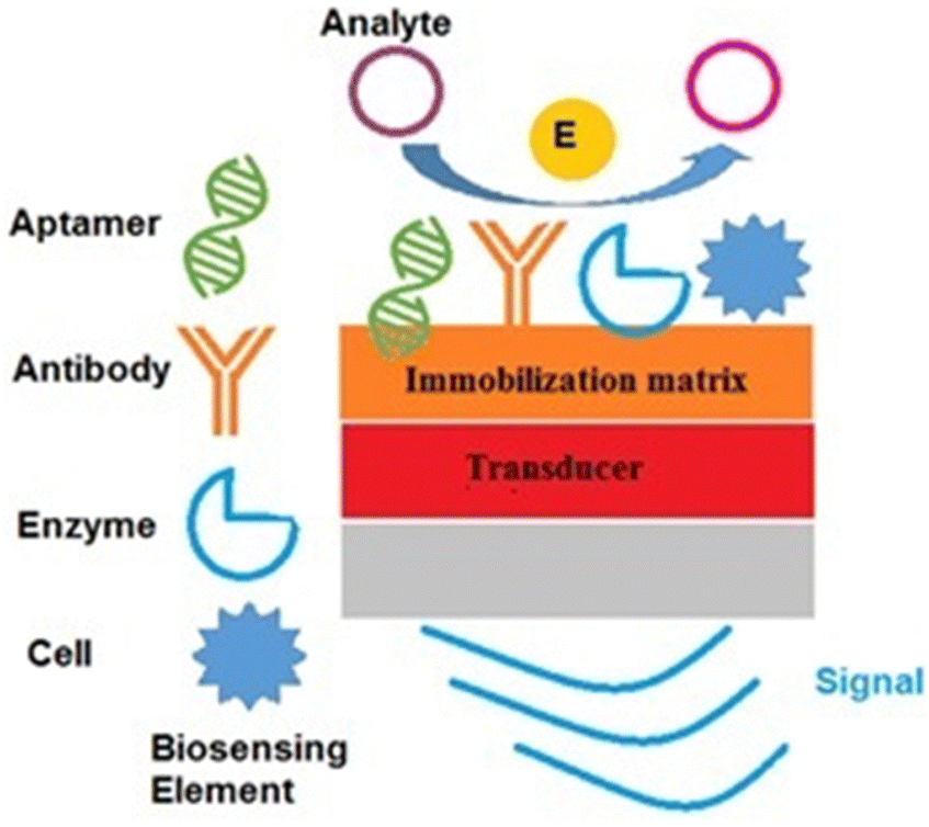 | ||
| Fig. 1 Components and mechanism of a biosensor. | ||
There have been multiple scientific works on borophene that include its synthesis, characterization, and applications in a variety of scientific fields in past years. However, to date, there has been much less work that reported the classification of borophenes on the basis of their dimensional properties and synthesis on one platform with a major focus on biosensing. This review provides the diverse approaches for the production of different dimensional borophenes over the past year on one platform with their drawbacks and advantages. Along with that, we compile the exploration of borophene in electrochemical biosensors in the past year, which will help the reader to explore the world of borophene in biosensor research area.
2. Synthesis of borophene nanomaterials
Borophene is a monoatomic layer of boron with a trigonal and hexagonal atomic ring arrangement differently that provides excellent material properties that have attracted significant attention in the past few years.15 Additionally, researchers are interested in exploring all the dimensional properties of borophene, so there has been exploration of different dimensional forms of borophene as shown in Fig. 2 by various research groups. 0D Borophene: 0D refers to quantum dots, which are semiconductor nanocrystals 0–10 nanometers in size that exhibit optical and electronic confinement and differ from their bulk as a result of quantum mechanics. Researchers have developed borophene quantum dots using various exfoliation techniques.28–31 1D Borophene: 1D nanomaterials are defined as linear architectures with a cross-sectional diameter of less than 100 nm, including nanowires, nanotubes, and nanorods. 1D nanomaterials can offer large surface area and efficient electron transport to achieve high electrochemical performance. Borophene nanoribbons are one example of 1D borophene.32 2D Borophene: 2D nanomaterials are the thinnest nanomaterials due to their thickness and dimensions on the nanoscale. These nanomaterials have a single-layered structure. These ultrathin nanomaterials can be synthesized using different techniques. Although “2D” refers to a single-layer, these nanosheets are often composed of a few layers. Researchers have synthesized 2D borophene using different synthesis strategies such as epitaxial growth, chemical vapor deposition, etc.10,11 3D Borophene: 3D borophene refers to the bulk form of borophene, in which multiple layers of borophene are arranged together to form a 3D structure. The properties of 3D borophene differ from its bulk. The unique dimensional forms of borophene provide excellent properties, and its potential applications in different fields have been explored. Scientists are continuously investigating borophene to unlock its wide range of applications that can be employed in various fields of research.33 In this section, we discuss the synthesis processes of different dimensions of borophene nanomaterials.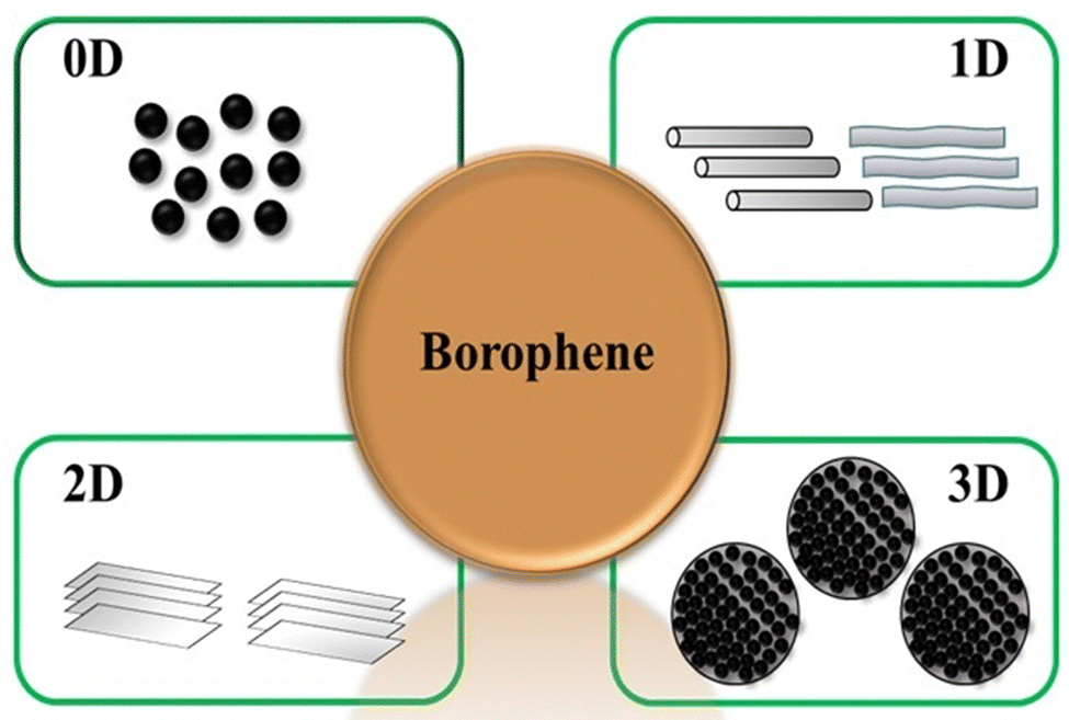 | ||
| Fig. 2 Classification of borophene on the basis of dimensional properties. | ||
2.1 Synthesis of 0D borophene nanomaterials
Quantum dots of borophene are 0D nanomaterials with exceptional properties in terms of quantum confinement, chemical stability,28 electronic mobility,29 Fermi band gap,30 capacitance,31 and conductivity,34 and physicochemical characteristics such as high quantum yield, Fermi band gap, size-dependent luminescence, etc., which provide great potential in the field of drug delivery systems, bio-imaging, and diagnostic applications. For the synthesis of 0D nanomaterials, there are two common approaches, bottom-up and top-down, in use, among which the top-down approaches have several advantages such as economic synthesis, purity, mass production, etc.35 Hao et al. reported the first experimental synthesis of boron quantum dots (BQDs) via a probe sonication technique. The researcher added 30 mg of boron powder to 15 ml of acetonitrile and probe-sonicated the mixture for 60 minutes using a 400 W probe-sonicator with a 20 kHz frequency in a cool bath. To extract the BQDs, the sample was centrifuged at 1500 rpm for 60 minutes and the supernatant was separated, which contained BQDs with an average lateral size of 2.46 nm and thickness of 2.81 nm according to TEM. Further characterization was carried out using AFM, XPS, FE-SEM, XRD, and UV-Visible spectroscopy. The quantum effect of the BQDs makes them a good component for advanced memory devices with an on/off ratio of 1000 times.15 He et al. prepared crystalline borophene quantum dots by a low-temperature-mediated probe-sonication-assisted liquid-phase exfoliation technique, as shown in Fig. 3(a); it is considered to be a top-down approach. In the experimental setup, first, boron powder was dispersed into propan-2-ol using ultra-sonication to form a homogenous solution. Then, the H3BO3 powder was dissolved completely into the solution and stirred until it became homogenous. Next, to this, H2O2 (30%) solution was added dropwise to the boronoic solution. The powder was ultrasonically dispersed at low temperature in the propan-2-ol solution using a high-power probe-type ultrasonicator, and the temperature of the sonicated dispersion was always kept at about 5 °C. After 5 h of ultrasonication, the product was separated using a centrifugation technique at a velocity of 2000 rpm for 1 h, and the supernatant was dialyzed. The dialyzed product was called crystalline borophene quantum dots, which are mono-dispersible with an average particle size of 3.5 nm, tremendous dispersibility, and high thermodynamic stability in propan-2-ol solution. Here, boric acid was an important factor for preparing the borophene quantum dots, along with hydrogen peroxide, which doubled the liquid–gas interfacial tension to peel the boron particles. Importantly, high-power treatment with the ultrasonic probe sonicator produces vacuum bubbles, which break down the boron particles into pieces. The average size of the borophene quantum dots was 3.5 nm according to TEM, as shown in Fig. 3(b). Their topographical height was 1–2 nm according to AFM, as shown in Fig. 3(c), which indicated a 1–3 layered material having an inter-planar distance of 0.22 nm with a clear dot structure in the HR-TEM image, as indicated in Fig. 3(d), atomic force microscopy, and HAADSTEM, respectively. Further validation of the crystalline borophene quantum dots was carried out using XPS, powder XRD, Raman spectroscopy, UV-Vis spectroscopy, FT-IR spectroscopy, and magnetic angle spinning (MAS) 11B-NMR spectroscopy, and photoluminescence spectroscopy.36 Further, Liu et al. prepared high-quality borophene quantum dots using a sonication-assisted liquid-phase top-down technique in which boron powder was first triturated in a mortar and pestle to make it thinner. Then, the obtained thinner paste was mixed with a solution of N-methyl pyrrolidone and butyl alcohol (6![[thin space (1/6-em)]](https://www.rsc.org/images/entities/char_2009.gif) :4) in a glass vial using a stirrer until a transparent solution was obtained. The homogenous borophene dispersion was probe-sonicated at low temperature for 120 minutes. The borophene suspension was separated using centrifugation for 20 min at 7000 rpm, and then a supernatant consisting of borophene quantum dots was obtained. By controlling the probe sonication time, they could control the borophene quantum dot sizes and uniform morphologies. The morphologies and size were characterized via SEM, FESEM, and TEM, the dimensions of the quantum dots were characterized using AFM, and elemental distribution, UV-Vis spectroscopy, XPS, and photoluminescence spectroscopy were carried out. The quantum dots had a size of 3.2 nm and topographical height of 2–3 nm. It was also reported that the synthesized nanomaterial had a 5–7 layered structure.39 Kailasa et al. synthesized ultra-small BQDs using a sonication-assisted liquid exfoliation method as shown in Fig. 3(e), in which bulk boron powder was dissolved in propan-2-ol using ultrasonication to form a transparent solution. The H3BO3 powder was added to H2O2 solvent and then continuously stirred for 5 h at room temperature. The reaction product was dispersed in isopropyl alcohol solution by means of a probe-sonicator of high power for 20 min at 5 °C. For purification, the mixture was centrifuged at 6000 rpm for 10 min. The BQDs were homogenously distributed in Milli-Q water, showed blue fluorescence at a 365 nm excitation wavelength, with dot shape. The average size of the particle was 1.61 ± 0.28 nm using HR-TEM analysis, and further characterization was carried out using XRD, FTIR, etc.37 Qureshi et al. prepared 0D borophene dots via two steps (i.e., sonication and hydrothermal methods) as shown in Fig. 3(f). First, a boron powder (1 mg mL−1) was dispersed in dimethyl formamide solution using an ultrasonicator at 400 W for 300 minutes to obtain the 2D borophene sheets. Afterward, the dispersion was centrifuged and the brown-coloured supernatant containing 2D borophene sheets was decanted into a Teflon-lined stainless autoclave assembly for 12 h of hydrothermal reaction at 180 °C. After the hydrothermal reaction, the reaction solution was cooled down and separated through a syringe filter to collect the 0D borophene dots. The borophene dot size was found to be 10 nm with an interplanar distance of 0.19 nm using TEM and HR-TEM, and other physicochemical validation were carried out using XRD, XPS, ultraviolet-visible spectroscopy, and photoluminescence spectroscopy.38,39
:4) in a glass vial using a stirrer until a transparent solution was obtained. The homogenous borophene dispersion was probe-sonicated at low temperature for 120 minutes. The borophene suspension was separated using centrifugation for 20 min at 7000 rpm, and then a supernatant consisting of borophene quantum dots was obtained. By controlling the probe sonication time, they could control the borophene quantum dot sizes and uniform morphologies. The morphologies and size were characterized via SEM, FESEM, and TEM, the dimensions of the quantum dots were characterized using AFM, and elemental distribution, UV-Vis spectroscopy, XPS, and photoluminescence spectroscopy were carried out. The quantum dots had a size of 3.2 nm and topographical height of 2–3 nm. It was also reported that the synthesized nanomaterial had a 5–7 layered structure.39 Kailasa et al. synthesized ultra-small BQDs using a sonication-assisted liquid exfoliation method as shown in Fig. 3(e), in which bulk boron powder was dissolved in propan-2-ol using ultrasonication to form a transparent solution. The H3BO3 powder was added to H2O2 solvent and then continuously stirred for 5 h at room temperature. The reaction product was dispersed in isopropyl alcohol solution by means of a probe-sonicator of high power for 20 min at 5 °C. For purification, the mixture was centrifuged at 6000 rpm for 10 min. The BQDs were homogenously distributed in Milli-Q water, showed blue fluorescence at a 365 nm excitation wavelength, with dot shape. The average size of the particle was 1.61 ± 0.28 nm using HR-TEM analysis, and further characterization was carried out using XRD, FTIR, etc.37 Qureshi et al. prepared 0D borophene dots via two steps (i.e., sonication and hydrothermal methods) as shown in Fig. 3(f). First, a boron powder (1 mg mL−1) was dispersed in dimethyl formamide solution using an ultrasonicator at 400 W for 300 minutes to obtain the 2D borophene sheets. Afterward, the dispersion was centrifuged and the brown-coloured supernatant containing 2D borophene sheets was decanted into a Teflon-lined stainless autoclave assembly for 12 h of hydrothermal reaction at 180 °C. After the hydrothermal reaction, the reaction solution was cooled down and separated through a syringe filter to collect the 0D borophene dots. The borophene dot size was found to be 10 nm with an interplanar distance of 0.19 nm using TEM and HR-TEM, and other physicochemical validation were carried out using XRD, XPS, ultraviolet-visible spectroscopy, and photoluminescence spectroscopy.38,39
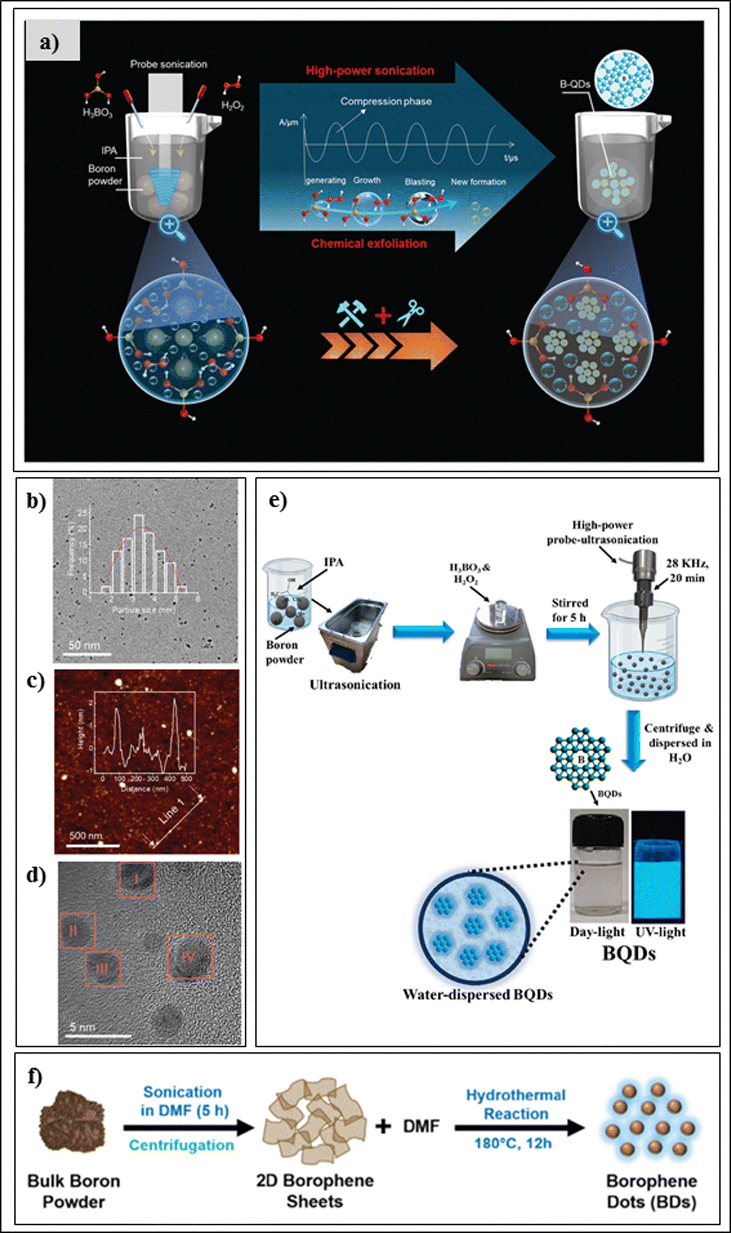 | ||
| Fig. 3 (a) Graphical illustration of the low-temperature ultrasonication-assisted liquid-phase exfoliation synthesis for crystalline borophene quantum dots. (b) TEM image of BQDs; the inset displays the BQD size distribution. (c) AFM image; the inset displays the topographic height parallel to the white line. (d) HR-TEM image of B-QDs. (a)–(d) Reproduced with permission from ref. 36. Creative Commons Attribution-Non Commercial 3.0 Unported License, (2021) Royal Society of Chemistry (RSC). (e) Graphical illustration of the ultrasonication-assisted liquid exfoliation synthesis procedure for borophene quantum dots (BQDs). Reproduced with permission from ref. 37. Copyright (2023), Elsevier. (f) Graphical illustration of the ultrasonication-assisted hydrothermal synthesis procedure of borophene dots (BDs). Reproduced with permission from ref. 38. Copyright (2023), Royal Society of Chemistry (RSC). | ||
2.2 Synthesis of 1D borophene nanomaterials
Like graphene, borophene nanoribbons (BNRs) have fascinating electronic properties40–43 and mechanical properties; their stabilities and electronic conductivities increase with their width.44 In the synthesis of 1D borophene, only one effort has been made: Chen et al. prepared single-atom-thick borophene nanoribbons using in-lab-developed low-temperature scanning tunneling microscope (STM) hyphenated molecular beam epitaxy in high-vacuum conditions. For the synthesis of the nanoribbons, first, an Ag crystal was cleaned multiple times using argon sputtering and annealing cycles. Then, preparation of the borophene nanoribbon on an Ag substrate was initiated via vapor deposition of evaporated pure boron atoms through an electron beam evaporator at a temperature of 570 K under high-vacuum conditions. The obtained borophene nanoribbons were a single atomic layer thick with a width of 10.3 mm and a length of hundreds of meters. The atomic structures of the nanoribbons were found to consist of chains of boron with variable widths parted by hexagonal void arrays. The effective production of borophene nanoribbons explores the field of 1D boron's allotrope.32 As we can see, limited research has been conducted in the field of one-dimensional borophene nanomaterials, so efforts should be made to synthesize different shapes of 1D borophene nanomaterials.2.3 Synthesis of 2D borophene nanomaterials
2D borophene nanomaterials are one of the lightest Dirac materials of single atom boron. They exhibit several excellent properties such as high Young's modulus, which provides high mechanical strength to the 2D borophene layer, 3-center 2-electron bonds, which provide electrical and thermal conductivity with different orientations of 2D borophene layers, which provide metallic anisotropy, etc., as compared to other nanomaterials.45 It has good chemical stability and Fermi resonance, which play a major role in conducting applications of borophene.14 However, 2D borophene synthesis has been the major challenge for researchers; thus, they have proposed different synthesis approaches for 2D borophene, such as molecular beam epitaxy, liquid sonication, chemical vapor deposition, electrochemical exfoliation, etc., as shown in Fig. 4.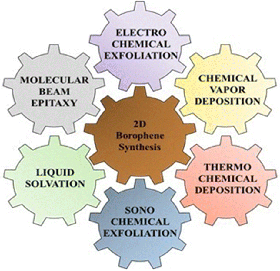 | ||
| Fig. 4 Different synthesis approaches for 2D borophene. | ||
Among the various synthesis approaches, top-down syntheses include various exfoliation techniques such as liquid-phase exfoliation, sonochemical exfoliation, electrochemical exfoliation, and mechanical exfoliation, which are cheaper and easier. For example, Kumar et al. reported the scalable synthesis of freestanding sheets of borophene through the process of sonochemical exfoliation. They reported the use of acetone and ethylene glycol as solvents to yield monolayers within a time duration of 12 h and 20 h, respectively, while other solvent systems did not yield any monolayers. Water and propan-2-ol displayed better exfoliation down to 2–3 monoatomic layers, but the borophene sheet sizes were very small. However, certain limitations, such as producing freestanding borophene, are challenging due to its intrinsic reactivity towards oxidation and degradation. The scaling of freestanding borophene hybrids is difficult for larger sizes, as quality and stability may be hampered.46 Cheng obtained borophene in its pure form by micromechanical exfoliation. Here, the pressure is applied vertically, which adheres the top layer of borophene with the help of double-sided tape. Various phases of exfoliation are carried out for up to 70 s and also cause strain in the system. The double-sided tape acts as a cushioning layer, which helps in sticking the adhesive surface of the tape to the top layer of boron. When the adhesion force breaks the van der Waals cohesive forces, exfoliation takes place. The folds and bends in the borophene sheet were confirmed using optical microscopy. However, the limitation of this method is that it cannot provide precise control over the thickness of borophene layers. Also, this process is time-consuming, as it is manual. Hence, large-scale production is not possible. This method often leads to contamination, as adhesive tapes are used in this process, and removing this contamination is quite difficult and challenging.14 Chowdhury et al. explored an electrochemical exfoliation technique by attaching boron to a heating coil. Here, the crystal lattice nature of the boron crystal can be altered through the sintering procedure under various optimum conditions. In this technique, the platinum behaves as an anode, and the cathode is made up of boron; they are dipped in an appropriate electrolytic solution. The temperature of the boron rod reached up to 600–1000 °C for the exfoliation of boron, leading to the formation of borophene flakes. The exfoliated 2D borophene was segregated from the electrolytic solution and washed several times to purify the flakes via a membrane filter, and they were further washed with Milli-Q water to eradicate impurities. They were then sonicated for 2 h in acetone, so that the layers were dispersed into the acetone and 2–3 layers borophene was synthesized. The sonicated dispersion was further centrifuged at 4000 rpm for 30 min to detach the borophene layers. Finally, the borophene was collected from the supernatant by the process of decantation. The borophene was collected and dried. After ultrasonication, 2D borophene layers were seen in the acetone, and this solution was centrifuged further. The characterization of borophene was carried out using zeta potential as well as particle size determination, and the size was found to be 400–600 nm. The main limitations faced by this method are temperature control, and management is required for maintaining the boron growth, as no graphs are available to date to show the correlation between the electrical conductivity and the temperature of the boron powder. As borophene is anisotropic in nature, its electrical conductivity can vary depending upon its crystallographic orientation. Hence, it may exhibit high carrier density and stiffness due to this property.13 De et al. obtained 2-D borophene sheets through the sonochemical exfoliation of amorphous boron in the liquid state. The authors used acetone as a solvent and dispersed a pre-defined amount of boron powder in it. The boron suspension was sonicated by means of a probe sonicator at 30 kHz for around 24 h. This sonicated suspension was centrifuged at 5000 rpm for 9–10 min. The resultant supernatant was collected separately as borophene. These borophene microstructures were characterized using HR-TEM, as shown in Fig. 5(a), and TEM. Moreover, AFM was used to analyze the thickness of the sheet, which was found to be 3.76 nm with 2–3 layers, as shown in Fig. 5(b).45
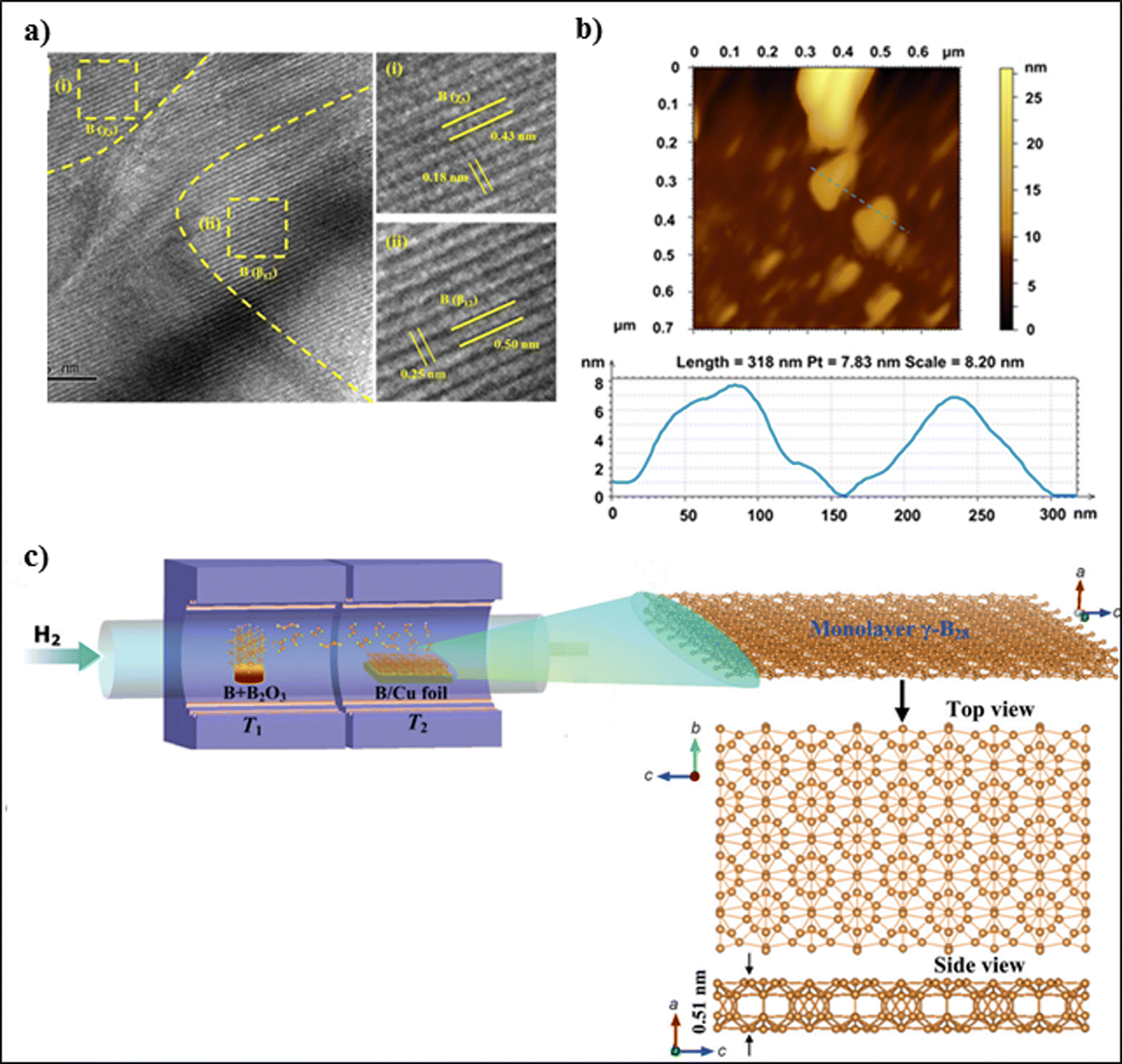 | ||
| Fig. 5 (a) HRTEM image of borophene showing lattice fringes corresponding to the (i) χ3 and (ii) β12 phases. (b) AFM image of borophene having a lateral dimension of 100–150 nm with thickness of 3.76 nm, corresponding to a 2–3 layer borophene sheet. (a), (b) Reproduced with permission from ref. 45. Copyright (2023), Royal Society of Chemistry (RSC). (c) Schematic representation of the home-made two-zone furnace used to obtain atomically thin 2D g-B28 films using CVD, with top and side views of the borophene monolayer. Reproduced with permission from ref. 47. Copyright (2015), John/Wiley & Sons. | ||
The bottom-up approach techniques include chemical vapor deposition, molecular beam epitaxy, thermal decomposition, and epitaxial growth. For example, Guoan et al. synthesized thin 2D films of boron on Cu foil, as shown in Fig. 5(c). They prepared the boron source by mixing 99.99% boron powder and 99.98% boron oxide powder in a weight ratio of 1:1 on the Cu foil. The dimension of the selected Cu foil was 25 μm. The powder mixture was further loaded in a quartz boat, and the thin films were grown on the Cu foil with a size of 3 × 2 cm2. Purging of the quartz tube was carried out using high-purity H2 gas for 30 min. This setup was further mounted in a two-zone chemical vapor deposition furnace. The temperature of the synthesis zone was maintained at 1000 °C, and that of the heating zone was maintained at 1100 °C; the zone temperatures were controlled separately. The Cu foil was annealed for 1 h at 1000 °C. Eventually, the temperature of the heating zone was increased to 1100 °C to synthesize B2O2 vapor, which was then transported to the synthesis zone by the high-purity H2 to form thin films of boron on the Cu foil. The boron films were characterized using optical microscopy. UV-Vis absorption spectra were obtained using a spectrometer at room temperature. However, a few limitations associated with this method are that perfect epitaxy cannot be achieved due to lattice mismatch and the formation of grains and defects during growth. Boron atoms possess lower surface diffusion on Cu, which may hinder the formation of uniform borophene sheets with large surface area.47 Tai et al. prepared borophene nanosheets through a CVD technique using a furnace with a dual-temperature zone. A carbon cloth was cut into small pieces and ultrasonicated with acetone, isopropanol, and alcohol for 15 min, and 500 mg sodium borohydride powder was used to grow borophene. The borophene nanosheets were analysed using ATR-FTIR spectroscopy, and the absorption peaks of borophene were observed at 2471 cm−1 and 2516 cm−1, indicating B–OH and BOH⋯H bonding, respectively. The optimum conditions for borophene synthesis are a temperature of 700 °C and 30 min, and the obtained borophene possesses excellent stability and corrosion resistance. A few limitations associated with this method are that borophene nanosheet may undergo degradation or structural modification during the hydrogen evolution reaction, which may affect its stability and catalytic performance.48 Liu et al. prepared 2D sheets of tetragonal borophene with higher stability and fabricated it on a 1 cm2 copper foil surface using a chemical vapor deposition technique under low pressure. They mixed crystalline boron powder and boron oxide powder in a mass ratio of 5:1 and placed the powder into a reaction container. A Cu foil (25 μm thickness) surface acted as a platform for the construction of 2D borophene, and the foil was annealed at 1000 °C for an hour. The surface temperature of the Cu foil increased to 600 °C in the presence of argon gas. Also, the temperature of the reaction container was increased to 1100 °C to generate boron vapour. The applied pressure must range from 87 Pa to 200 Pa and must be applied for 30–120 minutes. Later, the kiln must be cooled to room temperature in the presence of an inert gas. A brown-colored thin layer was deposited on the Cu surface. Eventually, a technique involving PMMA was used for the extraction of a 2D borophene layer from Cu onto PMMA. The PMMA was dipped into a ferric chloride solution for 2 h to remove the Cu foil. The extracted sample was dipped into an HCl solution for purification. As a result, the PMMA-covered 2D borophene was relocated onto the target substrate, and the PMMA could be removed by dissolving it in acetone at 80 °C. The thickness of the borophene sheets ranged from 10–20 nm according to STM. Through TEM and AFM analysis, it was found that the sheet exhibited a clear and sharp diffraction pattern, which confirmed the high crystallinity of the sheet. The average electrical conductivity of the single borophene sheet was found to be 4.5 × 10⁻¹ mS cm−1 and the energy band gap was 2.1 eV. However, there were a few limitations, such as the possibility of contamination or presence of impurities in the resulting borophene sheets. Scalability and reproducibility have been reported to be difficult to achieve using the CVD process.49 Hou et al. first predicted hydrogenated borophene to be an ideal material for use in nanoelectronics due to its outstanding electronic and mechanical properties and good stability. They firstly successfully synthesized ultrastable hydrogenated borophene with semiconducting and crystalline properties using an in situ three-step thermal decomposition process. The composition showed high stability in strong acidic and basic solvents. Initially, for the large-scale synthesis of freestanding borophene, an in situ three-step thermal decomposition process with sodium borohydride was developed for the growth without using any metal substrates. In step 1, the powder was heated to 490 °C at a rate of 10 °C min−1 for around 2 h. In the next step, the intermediates were heated to 550 °C at a rate of 5 °C min−1 for 30 min. In the last step, the powder was heated to 600 °C at a rate of 5 °C min−1 for 30 min for the large-scale production of borophene. It was characterized further using SEM, and the average lateral sides of the sheet were found to be 5.14 μm. The thickness of the sheet was measured using AFM, and it was found to be 0.78 μm. Due to its excellent stability and dispersion in various solvents like ethanol and water, it can be widely used in borophene-modified nano-devices.9 Fie et al. synthesized a 2-D borophene sheet using a thermal decomposition method. They mixed sodium borohydride powder with Cu, ground and mixed them in the presence of a homogenous dinitrogen atmosphere, and transferred the mixture into a tubular furnace. First, the furnace's temperature was increased to 490 °C with at 10 °C min−1 for 120 minutes. This led to the formation of an intermediate compound. The temperature was increased to 550 °C at a 5 °C min−1 heating rate, and kept there for 30 min, which caused the formation of a more stable compound. The kiln was then cooled to 27 °C. After multiple washing and dehydrating steps, the following sintering conditions were followed: the product was heated to 10−3 Pa and 700 °C at a rate of 50 °C min−1, respectively; they further dried the product at 800 °C. During the reaction, the pressure of the setup reached 50 Pa, and the temperature was maintained at 600 °C. The bulk composite material was cooled to room temperature, and the diameter was found to be 30 mm with a thickness of up to <3 mm. This method of synthesis presented a few limitations; for example, finding a substrate that is available for borophene growth and promotes the desired crystal structure while minimizing lattice mismatch is difficult. Also, the nucleation process is very difficult to control for the production of uniform sheets with desired orientation, as the boron atoms are highly reactive.49 Kehui et al. fabricated 2D boron sheets through molecular beam epitaxy using an Al (111) surface as a substrate. Aluminum has three free electrons, which effectively compensates the electron deficiency in borophene. They performed the experiments in a low-temperature-environment scanning tunneling microscope–molecular beam epitaxy system with a 10 mbar base pressure. The substrate was cleaned, and borophene layers were synthesized by vaporizing 99.99% boron on Al (111) using an electron beam evaporator with boron flux at a rate of 0.1 monolayer per minute at 500 K during the process. The borophene monolayer was characterized using HR-TEM, which revealed characteristic triangular, quasiperiodic corrugations. The dimensions of the triangular corrugations were found to be 40–60 pm, and the intra-distance between 6 and 7.5 nm. However, the limitation associated with this method is that Cu may diffuse into the films, leading to contamination.50 Luijten et al. achieved the growth of borophene; boron flux was initiated by the evaporation of a boron rod by utilizing an electron beam on a Ag (111) thin film with a thickness of 300 nm, and it was carried out on a mica substrate in the presence of UHV. Borophene was homogenously formed by maintaining the substrate temperature at 480 °C, but the limitation associated with this synthesis method is that the interface between the borophene film and mica substrate plays a very important role in determining the performance of the device. Hence, achieving a well-defined and controlled interface along with interfacial defects and minimal lattice mismatch is challenging and can affect the electrical and optical properties of the photodetector.51 Michael et al. found a substitute way of preparing a single-phase borophene domain using improved epitaxy. They synthesized borophene on a hot metallic substrate. Iridium (111) is the substrate of choice for borophene synthesis. Borazine was used as a precursor depending upon the dosing temperature, i.e., a temperature of 1100 °C was used to obtain a boron-enriched surface with lack of nitrogen. However, the associated limitation is that borazine is used as the precursor for the thermal decomposition process for the synthesis of borophene on iridium (111), but the availability of high-purity borazine is difficult, and its stability is hampered. Also, the decomposition of borazine may release by-products and contaminate the borophene film.52
2.4 Synthesis of 3D borophene nanomaterials
The structure of borophene has attracted the attention of the scientific community due to its light weight (desirable for improving the performance and efficiency of the material), high strength (useful for structural applications), unique flexibility and tunable electronic properties, low chemical reactivity, etc. These properties make it less prone to corrosion and oxidation with respect to other materials. On the basis of the literature review to date, there are no synthesis approaches available for the synthesis of 3D structures of borophene, but efforts towards computational approaches towards the synthesis of 3D borophene materials have been made. Borophene sheets are bonded and stacked on top of each other, leading to development of 3D layered structures constructed via interlayer interactions. These layered structures are more stable. Boron nitride has excellent thermal as well as electrical insulation, and thus exhibits great potential in the field of electronic packaging. Constructing a 3D network structure helps to increase the thermal conductivity through interconnected structures. They are dynamically stable, and hence represent an opportunity for the discovery of new structures for numerous applications such as microelectronic devices, nanoscale electronic devices, energy storage devices, etc.53 Muhammad et al. designed 3D porous structures based on two metallic borophenes, termed as 3D β12-borophene and 3D B7P2, using density functional theory. Both 3D materials are found to be stable electrically and mechanically. Hence, they designed it in such a way that it possesses the outstanding properties of 3D porous boron.54In Table 1, we have classified borophene materials as 0D, 1D, 2D, and 3D borophene on the basis of their dimensional property and summarized the different techniques for their synthesis with their drawbacks and advantages as compared to other synthesis approaches. The table also includes their applications and key references. This table provides a compilation of the different techniques for borophene nanomaterial synthesis for quick reference by the reader.
| S. no. | Material type | Material name | Synthesis approach | Advantages | Disadvantages/limitations | Application | Ref. |
|---|---|---|---|---|---|---|---|
| 1 | 0D | Boron quantum dots | Liquid-phase exfoliation via probe sonication | Low transition voltage of 0.5 V | High-frequency sonication | Advanced memory device | 15 |
| Crystalline borophene quantum dots | Low-temperature probe-sonication-assisted liquid-phase exfoliation | Good crystallinity quantum dots | Low-temperature reaction | Photoluminescence | 36 | ||
| High-quality borophene quantum dots | Sonication-assisted liquid-phase preparation | Uniform size distribution and good dispersibility | High-power probe sonication | Photovoltaic device | 39 | ||
| Borophene dots | Sonication-assisted hydrothermal method | Good electrochemical activity | Non-uniform size distribution | Photo-electrochemical water splitting | 38 | ||
| Borophene quantum dots | Sonication-assisted liquid exfoliation | Good fluorescence properties | Non-crystalline nature | Fluorescent sensor | 37 | ||
| 2 | 1D | Single-atom-thick borophene nanoribbons | Molecular beam epitaxy | Good conductivity | Anisotropic behavior | Material synthesis | 32 |
| 3 | 2D | 2-D borophene sheet | Sonochemical exfoliation | 6–8 layered borophene | Anisotropic electrical conductivity | Photocatalysis | 45 |
| Freestanding borophene sheet | Liquid-phase exfoliation | Superior performance in energy storage | Instability of freestanding borophene | Large-scale applications | 46 | ||
| 2-D borophene | Micromechanical exfoliation | Flexibility, high quality, higher conductivity | Difficult to regulate contamination | Hybrid energy storage, hydrogen storage | 14 | ||
| Borophene atomic layer | Electrochemical exfoliation | Faster, easier, and scalable | Temperature-dependent synthesis | Cathode design | 13 | ||
| 2D tetragonal borophene sheets | Low-pressure chemical vapor deposition | Larger surface area, and higher conductance of 2D borophene | Scalability and reproducibility | Optoelectronic detection | 49 | ||
| Borophene nanosheets | Chemical vapor deposition | Few-layered borophene with high capacitance | Borophene nanosheets may undergo degradation or structural modification | Electronics, sensors, catalysis | 48 | ||
| 2-D borophene sheet | Thermal decomposition | Good conductivity, flexible | Tedious nucleation process to form uniform sheets | Photodetector | 1 | ||
| Hydrogenated borophene | In situ thermal decomposition | Superior stability with low operating voltage of less than 0.35 V | Temperature-dependent synthesis | Memory devices | 9 | ||
| Single-phase borophene | Thermal decomposition | Controlled growth of borophene | Decomposition of borazine release by-products causes contamination of borophene | Optoelectronics, flexible electronics, and sensors | 52 | ||
| Honeycomb borophene | Epitaxial growth | 2–3 layered borophene with high conductivity | Limitations in terms of accessibility and preparation of the sample | 2D semiconductors or dielectrics | 61 | ||
| Borophene thin 2-D films | Epitaxial growth | Large surface area, higher conductivity | Low surface diffusion of boron on Cu, which hinders formation of uniform borophene sheets | Semiconductor, electronic and photonic devices | 47 | ||
| 2 D boron sheet | Molecular beam epitaxy | High strength, flexibility, lightweight | Cu may diffuse into the films, leading to contamination | Superconductive material | 50 | ||
| Borophene | Electron beam evaporation | High quality, purity, scalability and control over thickness | Interfacial defects and minimal lattice mismatch are challenging | Photodetector | 62 |
3. Biosensing applications of borophene nanomaterials
Borophene, which is made up of a monoatomic boron layer, has attracted significant attention due to its remarkable electronic, mechanical, and thermal characteristics. Among the various nanomaterials, borophene possesses higher electrical conductivity than other nanomaterials like graphene, germanene, etc. The surface functionalities on borophene, such as B–OH, and the electron-deficient nature of the boron atom in borophene make it a suitable platform as an immobilization matrix. This helps in covalent immobilization and physical adsorption of bioreceptor elements in biosensing platforms. Additionally, borophene has a high electroactive surface area, anisotropic nature, and high electron mobility, which result in enhanced analytical properties in biosensing applications. These properties are in line with the development of highly sensitive biosensors operated by a smartphone to accomplish early-stage POC diagnosis.8 Along with these wide-ranging applications of borophene, it has also been used in the fabrication of biosensing platforms for the detection of various diseases. Initially, Kailasa et al. used water-dispersed borophene quantum dots for the fabrication of a biosensor platform for sensing of dehydroepiandrosterone. The synthesized borophene quantum dots with a particle size of 1.61 ± 0.28 nm exhibit blue fluorescence under a 365 nm excitation wavelength and exhibit a quantum yield of 24.12%. This fluorescence property helps in the development of fluorescence biosensors. In the sensing results, it has been observed that the dehydroepiandrosterone selectively binds with borophene quantum dots and enhances the fluorescence of the borophene quantum dots (Fig. 6).37 This fluorescence-based biosensor is a ‘turn-on’ type sensor that can detect dehydroepiandrosterone within the range of 0.1 to 125 μM in plasma and urine-like biofluids with a detection limit of 18.72 nM.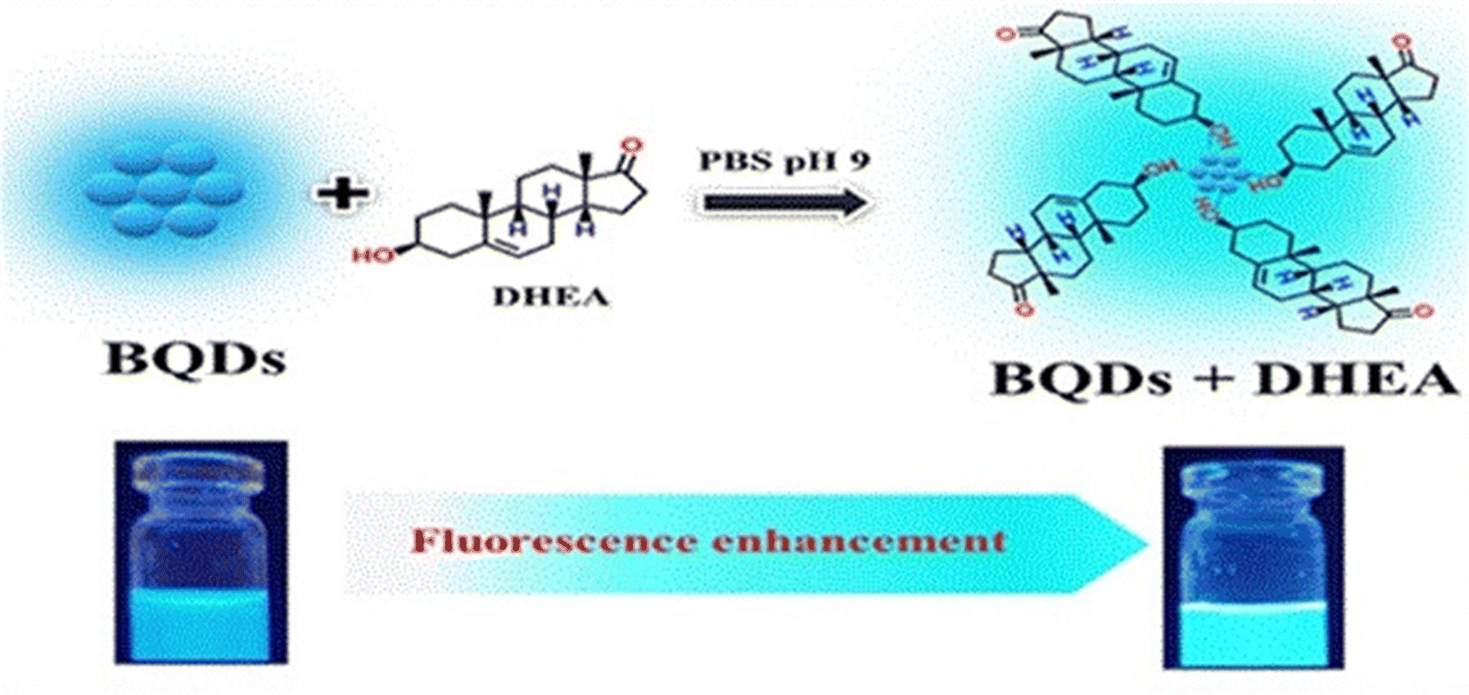 | ||
| Fig. 6 Dehydroepiandrosterone detection mechanism of BQDs. Reproduced with permission from ref. 37. Copyright (2023), Elsevier. | ||
Further, borophene was used for the development of an electrochemical biosensor for glucose detection. Baytemir et al. developed enzyme-free nickel phthalocyanine–borophene nanomaterial-based electrochemical sensors for glucose detection, in which the nickel phthalocyanine–borophene nanocomposite achieved an electrical conductivity of 9.5 × 10⁻⁹ S cm−1. This obtained conductivity is much higher (∼30000 times) than that of nickel phthalocyanine, which has a conductivity of 3 × 10⁻¹³ S cm−1. This alteration in the electrical conductivity of the composite is due to the high electron carrier ability of the borophene. The developed sensor can detect glucose with a linear detection range and sensitivity of 1.5–24 mM and 10.31 μA mM−1 cm−2, respectively, and a detection limit of 0.15 mM. In this work, the borophene nanosheets provide chemical stability and electron mobility towards nickel phthalocyanine for glucose detection.55 Tasaltin developed a polyacrylonitrile:β-rhombohedral borophene-based enzyme-free electrochemical biosensor for glucose detection. In this work, the centrosymmetric form of β-rhombohedral borophene was synthesized via a physical liquid exfoliation method, and the obtained product had a hexagonal morphology and a 0.41 nm inter-lattice dimension. To prepare the polyacrylonitrile:β borophene-based composite, a sonication-assisted exfoliation method was utilized. The polyacrylonitrile:β-rhombohedral borophene nanomaterial-based sensor for glucose sensing obtained a sensitivity and limit of detection of 8.43 μA mM−1 cm−2 and 0.099 mM, respectively, with a fast response time of 1 minute. Here, the β-rhombohedral borophene nanomaterial delivered a high charge kinetics mechanism to detect the glucose level more precisely at room temperature.56 Karakus et al. developed a polyaniline:borophene-based enzyme-free electrochemical biosensor for the detection of glucose. The developed sensor had an improved LOD and LOQ of 0.5 mM and 1.7 mM, respectively. In this work, they also concluded that the biosensor based on polyaniline–borophene has superior glucose sensing properties compared to polyaniline alone. The developed polyaniline–borophene-based biosensor can detect glucose in the range of 1–12 mM with a sensitivity of 96.93 μA mM−1 cm−2. The factors behind the obtained improved biosensing results are due to the presence of borophene.57 Tasaltin et al. developed an enzyme-free electrochemical sensor for the detection of urea using a highly sensitive and selective material, copper phthalocyanine–borophene nanocomposites. The developed sensor has an excellent sensitivity of 10.43 μA mM−1 cm−2 with a detection limit of 0.05 μM. Copper phthalocyanine borophene nanocomposites have a high selectivity in different matrices, such as various blood sugars. They can be used in highly competitive ion solutions due to the surface and chemical advantages of copper phthalocyanine. In this context, the phthalocyanine dyes have high electronic displacement and electrocatalytic properties, and the copper phthalocyanines possess extended π-electron conjugation systems, with redox-mediator and electrocatalytic properties. Borophene, which is a 2D highly conductive material, is used for electron transfer and electrical conductivity in the sensor. The urea detection mechanism in this biosensor was explained on the basis of two reactions, i.e., a catalytic reaction and an oxidation/reduction of the sensing material. In the catalytic reaction, urea produces 2 NH+ ions and CO−, and these ions increase the conductivity by providing more electron flux to the conduction band.58 Baytemir et al. developed a highly selective polyaniline–borophene nanocomposite-based enzyme-free electrochemical sensor for dopamine sensing. The developed dopamine biosensor has a detection range of 0.15625–5 μM with a sensitivity and limit of detection of 385.05 μA μM−1 cm−2 and 0.017 μM, respectively. In this work, the sensitivity of a PANI electrode was enhanced by 2D borophene through making polyaniline/borophene nanocomposites for the sensing application; among these components, borophene provides high electron conduction. Here, dopamine is detected on the principle of redox interaction between dopamine and the nanocomposite.59 Kumar et al. developed a PEDOT:PSS- and borophene-nanosheet-modified paper-based electrochemical biosensor for Serum Amyloid A (SAA) biomarker sensing. The developed biosensor has a limit of detection of 0.49 ng mL−1, a linear detection range of 1 ng mL−1–60 μg mL−1, and a stability of up to 42 days. The developed biosensor shows enhanced electrochemical performance, flexibility, and signal stability due to the incorporation of borophene and its unique properties.60 In Table 2, we have summarized the use of borophene nanomaterials in the fabrication of biosensing platforms for the detection of various analytes.
| S. no. | Disease | Biomarker | Biosensor type | Substrate material | Linear range | Detection limit | Sensitivity | Reproducibility | Stability | Ref. |
|---|---|---|---|---|---|---|---|---|---|---|
| 1. | Pediatric adrenocortical carcinoma | Dehydroepiandrosterone | Fluorescent “turn-on” sensor | Borophene quantum dots | 0.1–125 μM | 18.72 nM | — | — | Yes | 37 |
| 2. | Diabetes | Glucose | Non-enzymatic electrochemical biosensor | Nickel phthalocyanine–borophene | 1.5–24 mM | 0.15 mM | 10.31 μA mM−1 cm−2 | Yes | Yes | 55 |
| 3. | Polyacrylonitrile:β-rhombohedral borophene | 1.5–12 mM | 0.099 mM | 8.43 μA mM−1 cm−2 | Yes | Yes | 56 | |||
| 4. | Polyaniline:borophene | 1–12 mM | 0.5 mM | 96.93 μA mM−1 cm−2 | Yes | Yes | 57 | |||
| 5. | Kidney | Urea | Non-enzymatic electrochemical biosensor | Copper phthalocyanine borophene | — | 0.05 μM | 10.43 μA mM−1 cm−2 | Yes | Yes | 58 |
| 6. | Neurodegenerative | Dopamine | Non-enzymatic electrochemical biosensor | Polyaniline/borophene | 0.15625–5 μM | 0.017 μM | 385.05 μA μM−1 cm−2 | Yes | Yes | 59 |
| 7. | Swine flu | Serum Amyloid A | Electrochemical immunosensor | (PEDOT:PSS)/borophene | 1 ng mL−1–60 μg mL−1 | 0.49 ng mL−1 | 2.93 μA [log (μg mL−1)]−1 cm−2 | Yes | Yes | 60 |
4. Future prospects
Although various developments have been achieved in the field of synthesis of different-dimensional borophene materials, numerous challenges remain to be addressed in borophene synthesis. In the literature, the research community has reported many techniques for the synthesis of different-dimensional borophene materials, along with their advantages and limitations relative to the other synthesis techniques. However, there are substantial experimental studies on-going in this area to investigate the synthesis of borophene via easy synthesis techniques to create different-dimensional borophene nanomaterials with excellent properties. This would permit them to be used in real-world applications such as photovoltaic devices, thin-layer electronics, optoelectronics, sensor development, etc. As compared to synthesis of 0D and 2D borophene, there are very limited reports available regarding the synthesis and applications of 1D and 3D borophene. Thus, significant efforts have been made in the field of synthesis of borophene nanomaterials with different dimensional states, which enhances their prospects in a variety of research areas and in exploring the application roles of borophene. Moreover, the application of 0D, 1D, 2D, and 3D borophene nanomaterials should be extended to scientific research fields. Equally, the biosensing applications of borophene may be extended to other biomolecules (different analytes) for the diagnosis of various diseases as well as their prognosis. However, the synthesis of borophene and its biosensing applications remain in the early phase of research, and new synthetic methods for borophenes should be continuously discovered and explored because of its unique properties, which would expand its applications in current fields of science such as MEMS and NEMS. New ventures towards the profitable acceptance of borophene nanomaterials for numerous industrial and commercial applications should be supported. Finally, borophene nanomaterials are known as novel wonder materials in chemistry after carbon. In the near future, the variety of applications of borophene nanomaterials in multidisciplinary research will be expanded through new findings.5. Conclusions
Borophene has a unique electronic structure with n-type semiconductor properties when used as a single-layered structure. It also has other attractive properties, including light weight, good mechanical toughness, and superconducting properties (to compete with other existing 2D nanomaterials) that increase its application potential in the areas of flexible electronics, optoelectronics, and biosensors. Additionally, borophene exists in different dimensional states from 0D to 3D, which helps in tuning its properties for a wide range of research applications, such as the miniaturization of electronics, space engineering, textile production, etc. In this review, we have discussed the synthesis of different-dimensional borophene and its applications in the field of the fabrication of electrochemical biosensors in detail. Various synthesis approaches have been employed to fabricate borophene, such as chemical vapor deposition, liquid-phase exfoliation, sonochemical exfoliation techniques, mechanical exfoliation, molecular beam epitaxy, thermal decomposition, and epitaxial growth. Among them, CVD, MBE, thermal decomposition, and epitaxial growth have advantages like good crystalline growth and monolayer structure, but also have the limitations of laborious and costly techniques. In contrast to this, various exfoliation techniques, such as liquid-phase exfoliation, sonochemical exfoliation techniques, and mechanical exfoliation, have advantages over other synthesis techniques, such as cheaper synthesis for 0D borophene and crystalline nature, but also have the limitations of lower product yield, and batch-to-batch variation. From the present investigation in the field of borophene, it is found that very few works have been carried out in this field, particularly in the synthesis of 1D and 3D borophene nanomaterials. Efforts should be made towards the synthesis of three-dimensional borophene nanomaterials and their use in other biomedical fields, such as the fabrication of point-of-care devices for communicable and non-communicable diseases, fluorescent biosensors, drug delivery, gene delivery, scaffold synthesis, etc.Abbreviations
| 0D | 0-Dimensional |
| 1D | 1-Dimensional |
| 2D | 2-Dimensional |
| 3D | 3-Dimensional |
| CVD | Chemical vapor deposition |
| IUPAC | International union of pure and applied chemistry |
| TEM | Transmission electron microscopy |
| AFM | Atomic force microscopy |
| HR-TEM | High resolution transmission electron microscopy |
| HAADSTEM | High angle annular dark field imaging scanning transmission electron microscopy |
| XPS | X-ray photoelectron spectroscopy |
| XRD | X-ray diffraction |
| UV-Vis | Ultraviolet-visible |
| FT-IR | Fourier transform infrared |
| MAS | Magnetic angle spinning |
| NMR | Nuclear magnetic resonance |
| SEM | Scanning electron microscopy |
| FESEM | Field emission scanning electron microscopy |
| BQD | Borophene quantum dots |
| BNR | Borophene nanoribbons |
| STM | Scanning tunneling microscopy |
| PMMA | Polymethyl methacrylate |
| UHV | Ultra high vacuum |
| ATR | Attenuated total reflectance |
| DHEA | Dehydroepiandrosterone |
| LOD | Limit of detection |
| LOQ | Limit of quantitation |
| PANI | Polyaniline |
| MEMS | Micro electro mechanical systems |
| NEMS | Nano electro mechanical systems |
Author contributions
Gourang Hari Gupta: writing – original draft and editing, conceptualization, data curation, investigation, resources, visualization; Shikha Kadakia: writing – original draft, data curation, visualization, resources; Darshan Agiwal: writing – original draft, resources; Tanya Keshari: writing – original draft, resources; Suveen Kumar: conceptualization, investigation, project administration, supervision, validation, writing – review and editing.Conflicts of interest
The authors declare no conflicts of interest.Acknowledgements
The authors express their sincere gratitude to the National Institute of Pharmaceutical Education and Research-Ahmedabad for the financial support to accomplish the work.References
- Y. V. Kaneti, D. P. Benu, X. Xu, B. Yuliarto, Y. Yamauchi and D. Golberg, Chem. Rev., 2021, 122, 1000–1051 CrossRef
.
- P. Ranjan, J. M. Lee, P. Kumar and A. Vinu, Adv. Mater., 2020, 32, 2000531 CrossRef CAS PubMed
- M. Ashton, J. Paul, S. B. Sinnott and R. G. Hennig, Phys. Rev. Lett., 2017, 118, 106101 CrossRef
- Z. A. Piazza, H.-S. Hu, W.-L. Li, Y.-F. Zhao, J. Li and L.-S. Wang, Nat. Commun., 2014, 5, 3113 CrossRef
- G. Forte, A. La Magna, I. Deretzis and R. Pucci, Nanoscale Res. Lett., 2010, 5, 158–163 CrossRef CAS
- Y. Huang, S. N. Shirodkar and B. I. Yakobson, J. Am. Chem. Soc., 2017, 139, 17181–17185 CrossRef CAS
- X. Liu, Z. Zhang, L. Wang, B. I. Yakobson and M. C. Hersam, Nat. Mater., 2018, 17, 783–788 CrossRef CAS PubMed
- P. K. Sharma, A. Ruotolo, R. Khan, Y. K. Mishra, N. K. Kaushik, N.-Y. Kim and A. K. Kaushik, Mater. Lett., 2022, 308, 131089 CrossRef
- C. Hou, G. Tai, J. Hao, L. Sheng, B. Liu and Z. Wu, Angew. Chem., Int. Ed., 2020, 59, 10819–10825 CrossRef CAS PubMed
- A. J. Mannix, X. Zhou, B. Kiraly, J. D. Wood, D. Alducin, B. D. Myers, X. Liu and B. L. Fisher, Science, 2015, 350, 1513 CrossRef CAS PubMed
- B. Feng, J. Zhang, Q. Zhong, W. Li, S. Li, H. Li, P. Cheng, S. Meng, L. Chen and K. Wu, Nat. Chem., 2016, 8, 563–568 CrossRef CAS
- A. Mazaheri, M. Javadi and Y. Abdi, ACS Appl. Mater. Interfaces, 2021, 13, 8844–8850 CrossRef CAS
- M. A. Chowdhury, M. M. K. Uddin, M. B. A. Shuvho, M. Rana and N. Hossain, Appl. Surf. Sci. Adv., 2022, 11, 100308 CrossRef
- S. Chahal, P. Ranjan, M. Motlag, S. S. Yamijala, D. J. Late, E. H. S. Sadki, G. J. Cheng and P. Kumar, Adv. Mater., 2021, 33, 2102039 CrossRef CAS PubMed
- J. Hao, G. Tai, J. Zhou, R. Wang, C. Hou and W. Guo, ACS Appl. Mater. Interfaces, 2020, 12, 17669–17675 CrossRef CAS
- C. Hou, G. Tai, B. Liu, Z. Wu and Y. Yin, Nano Res., 2021, 1–8 CAS
- C. Hou, G. Tai, Y. Liu, Z. Wu, Z. Wu and X. Liang, J. Mater. Chem. A, 2021, 9, 13100–13108 RSC
- X. Liu, C. Hou, Y. Liu, S. Chen, Z. Wu, X. Liang and G. Tai, J. Mater. Chem. A, 2023, 11, 24789–24799 RSC
- C. Hou, G. Tai, Y. Liu and X. Liu, Nano Res., 2022, 1–8 CAS
- C. Hou, G. Tai, Y. Liu, R. Liu, X. Liang, Z. Wu and Z. Wu, Nano Energy, 2022, 97, 107189 CrossRef CAS
- C. Hou, G. Tai, Y. Liu, Z. Wu, X. Liang and X. Liu, Nano Res. Energy, 2023, 2, e9120051 CrossRef
- A. G. Alharbi, V. Sorathiya and S. Lavadiya, Photonics, 2022, 9, 1–13 Search PubMed
- A. Verma, A. K. Sharma and Y. K. Prajapati, Opt. Mater., 2021, 119, 111355 CrossRef CAS
- Y. Rasmi, X. Li, J. Khan, T. Ozer and J. R. Choi, Anal. Bioanal. Chem., 2021, 413, 4137–4159 CrossRef CAS PubMed
- M. Nič, J. Jirát, B. Košata, A. Jenkins and A. McNaught, IUPAC, Res. Triagle Park. NC, 2016 Search PubMed
- S. Kurbanoglu, C. Erkmen and B. Uslu, TrAC, Trends Anal. Chem., 2020, 124, 115809 CrossRef CAS
- J. Kim, A. S. Campbell, B. E.-F. de Ávila and J. Wang, Nat. Biotechnol., 2019, 37, 389–406 CrossRef CAS PubMed
- G. Eda, H. Yamaguchi, D. Voiry, T. Fujita, M. Chen and M. Chhowalla, Nano Lett., 2011, 11, 5111–5116 CrossRef CAS PubMed
- S. Balendhran, J. Deng, J. Z. Ou, S. Walia, J. Scott, J. Tang, K. L. Wang, M. R. Field, S. Russo and S. Zhuiykov, Adv. Mater., 2013, 25, 108 CrossRef
- Q. Weng, G. Li, X. Feng, K. Nielsch, D. Golberg and O. G. Schmidt, Adv. Mater., 2018, 30, 1801600 CrossRef PubMed
- D. Su, A. McDonagh, S. Qiao and G. Wang, Adv. Mater., 2017, 29, 1604007 CrossRef
- Q. Zhong, L. Kong, J. Gou, W. Li, S. Sheng, S. Yang, P. Cheng, H. Li, K. Wu and L. Chen, Phys. Rev. Mater., 2017, 1, 21001 CrossRef
- L. Cui, T. Song, J. Cai, X. Cui, Z. Liu and J. Zhao, Phys. Rev. B, 2020, 102, 155133 CrossRef CAS
- B. Uchoa and A. H. C. Neto, Phys. Rev. Lett., 2007, 98, 146801 CrossRef
- J. Zhu, Y. Dong, S. Zhang and Z. Fan, Acta Phys.-Chim. Sin., 2020, 36, 1–16 Search PubMed
- H. Wang, D. An, M. Wang, L. Sun, Y. Li, H. Li, N. Li, S. Hu and Y.-B. He, Mater. Adv., 2021, 2, 3269–3273 RSC
- D. J. Joshi, N. I. Malek, T. J. Park and S. K. Kailasa, J. Mol. Liq., 2023, 122294 CrossRef CAS
- M. K. Mohanta and M. Qureshi, Chem. Commun., 2023, 59, 1955–1958 RSC
- A. Zhao, Y. Han, Y. Che, Q. Liu, X. Wang, Q. Li, J. Sun, Z. Lei, X. He and Z.-H. Liu, J. Mater. Chem. A, 2021, 9, 24036–24043 RSC
- Y. Ding, X. Yang and J. Ni, Appl. Phys. Lett., 2009 Search PubMed
- R. Atif, I. Shyha and F. Inam, Polymers, 2016, 8, 281 CrossRef
- Y. Liu, Y.-J. Dong, Z. Tang, X.-F. Wang, L. Wang, T. Hou, H. Lin and Y. Li, J. Mater. Chem. C, 2016, 4, 6380–6385 RSC
- S. Saxena and T. A. Tyson, Phys. Rev. Lett., 2010, 104, 245502 CrossRef PubMed
- V. Barone, O. Hod and G. E. Scuseria, Nano Lett., 2006, 6, 2748–2754 CrossRef CAS PubMed
- B. Pratihar, A. Jana, S. Biswas and S. De, Catal. Sci. Technol., 2023, 13, 1558–1570 RSC
- P. Ranjan, T. K. Sahu, R. Bhushan, S. S. Yamijala, D. J. Late, P. Kumar and A. Vinu, Adv. Mater., 2019, 31, 1900353 CrossRef PubMed
- G. Tai, T. Hu, Y. Zhou, X. Wang, J. Kong, T. Zeng, Y. You and Q. Wang, Angew. Chem., Int. Ed., 2015, 54, 15473–15477 CrossRef CAS PubMed
- G. Tai, M. Xu, C. Hou, R. Liu, X. Liang and Z. Wu, ACS Appl. Mater. Interfaces, 2021, 13, 60987–60994 CrossRef CAS PubMed
- Z. Guo, H. Lin, H. Zhang, Y. Tian, Y. Chen, J. Chen, S. Deng and F. Liu, Cryst. Growth Des., 2023, 4506–4513 CrossRef CAS
- W. Li, Sci. Bull., 2018, 63, 282–286 CrossRef CAS PubMed
- X. Liu, Z. Wei, I. Balla, A. J. Mannix, N. P. Guisinger, E. Luijten and M. C. Hersam, Sci. Adv., 2017, 3, e1602356 CrossRef PubMed
- K. M. Omambac, M. Petrovic, P. Bampoulis, C. Brand, M. A. Kriegel, P. Dreher, D. Janoschka, U. Hagemann, N. Hartmann and P. Valerius, ACS Nano, 2021, 15, 7421–7429 CrossRef CAS PubMed
- D. Li, Q. Tang, J. He, B. Li, G. Ding, C. Feng, H. Zhou and G. Zhang, ACS Omega, 2019, 4, 8015–8021 CrossRef CAS PubMed
- I. Muhammad, U. Younis, H. Xie, A. A. Khan, A. Khaliq, A. Samad, U. Schwingenschlogl and Q. Sun, Chem. Mater., 2021, 33, 2976–2983 CrossRef CAS
- G. Baytemir, İ. Gürol, S. Karakuş, C. Taşaltın and N. Taşaltın, J. Mater. Sci.: Mater. Electron., 2022, 33, 16586–16596 CrossRef CAS
- C. Taşaltın, Inorg. Chem. Commun., 2021, 133, 108973 CrossRef
- C. Taşaltın, T. A. Türkmen, N. Taşaltın and S. Karakuş, J. Mater. Sci.: Mater. Electron., 2021, 32, 10750–10760 CrossRef
- S. Güngör, C. Taşaltın, İ. Gürol, G. Baytemir, S. Karakuş and N. Taşaltın, Appl. Phys. A: Mater. Sci. Process., 2022, 128, 89 CrossRef
- G. Baytemir, Appl. Phys. A: Mater. Sci. Process., 2023, 129, 85 CrossRef CAS
- Y. Kumar, S. Shankar, R. Chandra and S. Kumar, Microchem. J., 2023, 194, 109318 CrossRef CAS
- K. Pu, X. Dai, Y. Bu, Y. Guo, Q. Jin, J. Song, T. Zhao and T. Lei, J. Phys. Chem. C, 2021, 125, 8589–8596 CrossRef CAS
- Z. Wu, G. Tai, R. Liu, C. Hou, W. Shao, X. Liang and Z. Wu, ACS Appl. Mater. Interfaces, 2021, 13, 31808–31815 CrossRef CAS PubMed
| This journal is © The Royal Society of Chemistry 2024 |