
 Open Access Article
 This Open Access Article is licensed under a
 Creative Commons Attribution 3.0 Unported Licence
Development of wafer-scale multifunctional nanophotonic neural probes for brain activity mapping
Fu Der
Chen
 *ab,
Ankita
Sharma
ab,
David A.
Roszko
ab,
Tianyuan
Xue
ab,
Xin
Mu
ab,
Xianshu
Luo
c,
Hongyao
Chua
c,
Patrick Guo-Qiang
Lo
c,
Wesley D.
Sacher
a and
Joyce K. S.
Poon
*ab
*ab,
Ankita
Sharma
ab,
David A.
Roszko
ab,
Tianyuan
Xue
ab,
Xin
Mu
ab,
Xianshu
Luo
c,
Hongyao
Chua
c,
Patrick Guo-Qiang
Lo
c,
Wesley D.
Sacher
a and
Joyce K. S.
Poon
*ab
aMax Planck Institute of Microstructure Physics, Weinberg 2, 06120 Halle, Germany. E-mail: fu-der.chen@mpi-halle.mpg.de; joyce.poon@mpi-halle.mpg.de
bDepartment of Electrical and Computer Engineering, University of Toronto, 10 King's College Road, Toronto, Ontario M5S 3G4, Canada
cAdvanced Micro Foundry Pte Ltd, 11 Science Park Road, Singapore Science Park II, 117685, Singapore
First published on 26th March 2024
Abstract
Optical techniques, such as optogenetic stimulation and functional fluorescence imaging, have been revolutionary for neuroscience by enabling neural circuit analysis with cell-type specificity. To probe deep brain regions, implantable light sources are crucial. Silicon photonics, commonly used for data communications, shows great promise in creating implantable devices with complex optical systems in a compact form factor compatible with high volume manufacturing practices. This article reviews recent developments of wafer-scale multifunctional nanophotonic neural probes. The probes can be realized on 200 or 300 mm wafers in commercial foundries and integrate light emitters for photostimulation, microelectrodes for electrophysiological recording, and microfluidic channels for chemical delivery and sampling. By integrating active optical devices to the probes, denser emitter arrays, enhanced on-chip biosensing, and increased ease of use may be realized. Silicon photonics technology makes possible highly versatile implantable neural probes that can transform neuroscience experiments.
 Fu-Der Chen | Fu-Der Chen received his B.A.Sc. and M.A.Sc. degrees in Electrical and Computer Engineering from the University of Toronto, Ontario, Canada, in 2017 and 2019, respectively. He is pursuing a Ph.D. degree in Electrical and Computer Engineering at the University of Toronto while conducting his research at the Max Planck Institute of Microstructure Physics and the Krembil Brain Institute. His research interest is to develop implantable silicon probes with monolithically integrated nanophotonic devices for optogenetic stimulation and microelectrodes for electrophysiological recording. |
 Ankita Sharma | Ankita Sharma is currently pursuing her Ph.D. degree in Electrical and Computer Engineering at the University of Toronto while conducting her research at the Max Planck Institute of Microstructure Physics under the supervision of Prof. Joyce Poon. Her main research focus is on integrated photonic circuits for beam-steering applications. Ankita earned her B.S. degree from the California Institute of Technology in 2018 and M.S. degree from ETH Zurich in 2020, both in the field of Electrical Engineering. |
 David A. Roszko | David A. Roszko completed his BSc degree in Electrical Engineering and MSc degree in Neuroscience at the University of Alberta, Canada. He is currently pursuing a PhD degree in Electrical and Computer Engineering at the University of Toronto, Canada, with research conducted at the Max Planck Institute of Microstructure Physics, Germany. His research focuses on the design, characterization, and application of nanophotonic neural interfaces for dual-color optogenetic stimulation and electrophysiological recording. |
 Tianyuan Xue | Tianyuan Xue received his B.A.Sc. and M.A.Sc. degrees from the University of Toronto, Ontario, Canada for Engineering Science majoring in Physics and Electrical and Computer Engineering in 2016 and 2020, respectively. Since 2020, he has been pursuing a Ph.D. degree in Electrical and Computer Engineering at the University of Toronto while conducting his research at the Max Planck Institute of Microstructure Physics. His research interests include beam forming through grating coupler design. |
 Xin Mu | Xin Mu is a Ph.D. student in Electrical and Computer Engineering at the University of Toronto while conducting her research at the Max Planck Institute of Microstructure Physics under the supervision of Prof. Joyce Poon. Her current research interests are focused on implantable silicon photonic neural probes with microfluidic capability for chemical injection and sampling. She received her B.S. (2017) and M.S degrees (2020) in Electronic Engineering from Tsinghua University, China. |
Wesley D. Sacher is a research group leader at the Max Planck Institute of Microstructure Physics. He received his PhD degree in Electrical and Computer Engineering from the University of Toronto in 2015. From 2015 to 2018, he was a postdoctoral scholar at the California Institute of Technology. His current research is focused on integrated photonics for visible wavelengths and neurotechnologies for optogenetics and functional imaging. |
 Joyce Poon | Joyce Poon is a Director at the Max Planck Institute of Microstructure Physics, a Professor of Electrical and Computer Engineering at the University of Toronto, and an Honorary Professor in the Faculty of Electrical Engineering and Computer Science at the Technical University of Berlin. She and her team specialize in integrated photonics on silicon. Poon obtained her Ph.D. and M.S. degrees in Electrical Engineering from the California Institute of Technology in 2007 and 2003, respectively, and B.A.Sc. degree in Engineering Science (physics option) from the University of Toronto in 2002. She is an Optica Fellow and a Fellow of the IEEE. |
1 Introduction
The brain holds vast potential for discovery, with applications ranging from therapies for neural disorders and diseases to the advancement of artificial intelligence.1,2 This motivation has led to major research initiatives globally with the mission of mapping the structural and functional characteristics of the mammalian brain.3–7 These projects, such as the BRAIN initiative in the United States, the Human Brain Project in Europe, the China Brain Project, the Brain/MINDS project in Japan, and the Korea Brain Initiative, have spurred the development of a wide range of innovative neurotechnologies, ranging from molecular genetic to hardware tools,8–10 to map brain activity with cellular resolution.An important class of tools is implantable probes that can stimulate and record neuronal activity in deep brain regions at depths beyond the attenuation length of visible light (<1 mm from the surface of the brain11), where the beam intensity decreases by a factor of 1/e with reduced spatial resolution. An example of a technology that has been steadily gaining traction in the neuroscience community in recent years is Neuropixels, a complementary metal-oxide semiconductor (CMOS)-based implantable silicon (Si) neural probe with up to 5120 recording sites.12,13 This unprecedentedly high electrode density is revolutionizing large-scale extracellular recording, enabling detailed studies of neuronal spiking activity, the primary communication signal between neurons, in different brain regions of a mouse during complex behaviors.14 On the other hand, extracellular electrophysiology can have sampling bias toward cells with high firing rates.15 Also, complementary techniques are still required to validate the identification of certain cell types through extracellular recordings.16,17 These shortcomings can be overcome with optogenetics and functional fluorescence imaging, where genetic modifications make neurons of specific cell types interrogable with light.8,9 For single-photon absorption, optical excitation typically uses a wavelength in the visible spectrum. For example, for optogenetic photostimulation, channelrhodopsin-2 (ChR2),18 the most widely used light-sensitive ion channel, opens upon exposure to blue light (λ ∼ 470 nm (ref. 19)) to trigger action potentials; and genetically-encoded fluorescent indicators that are reporters of neural activity, such as GCaMP for calcium, QuasAr for voltage, and dLight for dopamine, also absorb wavelengths in the visible spectrum.20–22 These optical techniques for mapping neural circuits motivate the development of implantable microtechnologies that bring light into deep brain regions, akin to electrophysiological probes.
A simple way to deliver light into the brain is to implant a single-core optical fiber, but conventional fibers typically have larger cross-sectional areas on the order of 10−2 to 10−1 mm2 (ref. 23) compared to Si probes (10−3 mm2). Conventional fiber implants without additional wavefront compensation also lack selectivity for multiple emission sites and important functions, such as electrophysiological recording. Optical fibers can be implanted with Si electrophysiological probes,24,25 but increasing the number of optical channels to stimulate multiple brain regions requires implanting several optical fibers, which can be challenging to implement at scale and high density. Custom multifunctional fiber implants with integrated microelectrodes and microfluidic channels enable electrophysiological recordings and chemical delivery with a single implant,26,27 but they typically have a low number (<10) of addressable light emitters, electrodes, and fluidic channels demonstrated in in vivo experiments.
In contrast, Si-based neural probes integrated with optoelectronic materials can realize more than a hundred microscale light emitting diodes (either μ-LEDs28–31 or μ-OLEDs32) and microelectrodes on probe shanks. For example, ref. 31 reported the integration of 256 electrodes and 128 μ-LEDs on a probe. However, each emitter is limited to a Lambertian emission profile, constraining its versatility for neuroscience applications requiring patterned illumination, such as light-sheet imaging. In addition, the low wall-plug efficiency of the μ-LEDs and μ-OLEDs can limit the optical output power to tens of μW or less to minimize heating in brain tissue or to avoid interconnect failure due to the drive current.28,29,31,33 This limitation means that the devices may be less suitable for applications that require high power to illuminate large brain volumes over long durations.34,35
An alternative class of light delivery implants use micro- and nano-scale waveguides patterned on Si wafers. The waveguides bring light from an external light source into the brain. The light source(s), being physically separated from brain tissues, reduce the risk of inducing thermal damage to the brain. Initially, the probes used microscale multimode (MM) waveguides that are about 10 to 40 μm wide, >5 μm thick, and made of SU-8 or SiON, which emit light from the distal end into the brain.36–42 In recent years, the advent of Si nanophotonic technology, with photonic components fabricated using CMOS-compatible processes, has made it possible to realize complex and densely integrated photonic circuits at scale, on 200 or 300 mm diameter Si wafers and manufactured in foundries.43 This opens the opportunity to develop nanophotonic neural implants that are mass-manufacturable, have complex optical functionalities, and are suitable for cointegration with other technologies. Such nanophotonic circuits have submicron feature sizes and chiefly use single-mode (SM) waveguides, which enable designs of efficient passive and active components, such as grating couplers, power dividers, wavelength multiplexers, polarization controllers, and optical switches.43,44 Recently, ref. 45 reported the monolithic integration of nanophotonic waveguides on CMOS-based neural probes with 960 electrodes and 28 grating emitters, with 14 emitters per wavelength of 450 and 638 nm for dual-color stimulation. Foundry fabrication is critical for such highly integrated nanophotonic neural probes. Table 1 summarizes the state-of-the-art Si neural probes with light emission capabilities, reporting the maximum number of electrodes, emitters, and microfluidic channels realized on the devices by the same research group.
| Emitter type | Beam emission profile | Implant cross-sectional areaa [μm2] | # of Si shanks | # of electrodes | # of independently addressable emitters | Wavelengths [nm] | # of microfluidic outlets | Foundry fabricated probe? | Ref. |
|---|---|---|---|---|---|---|---|---|---|
| a Only report the cross-sectional area of a single shank unless specified otherwise. b We have demonstrated emitters with various beam characteristics utilizing a single-layer SiN waveguide, including low-divergence beams, light sheets, steerable beams, and focusing beams.46–52 c Cross-sectional area of a silicon shank + a 3D printed microfluidic channel. d Ref. 47–50 reported with wavelength operation at 488 nm and ref. 51 reported at 488 and 594 nm. e Cross-sectional area of a silicon shank + a waveguide fabricated on the shank. f Width estimated from Fig. 1b in ref. 37. g Electrodes and optical emitters are on separate devices. h Peak emission wavelengths estimated from Fig. 2d in ref. 32. i The cross-sectional area of the shank of the electrophysiological silicon probe + the fiber. j Only the electrophysiological Si probe was fabricated in the foundry. k Probe thickness is not reported. | |||||||||
| SiN waveguide | Flexibleb | 70 to 150 × 50 to 100 + 80 × 30c | Up to 4 | 72 | 16 | 488, 594d | 1 | Yes | 46–52, 55 |
| SiN waveguide | Diverging | 70 × 33 | 1 | 960 | 14 × 2 colors | 450, 638 | NA | Yes | 45 |
| SiN waveguide | Low-divergence or focusing | 45 × 15 | 1 | 64 | 3 × 2 colors | 450, 655 | NA | No | 57–59 |
| SiN waveguide | Low-divergence | >100 × 250 | 1 | 4 | 8 | 473 | NA | No | 60 |
| SiN waveguide | Low-divergence | 100 × 30 | 1 | 24 | 6 × 2 colors | 450, 590 | NA | Yes | 61 |
| SiN waveguide | Low-divergence | 100 × 23.5 | 2 | 40 | 2 | 532 | NA | No | 62, 63 |
| SiN waveguide | Low-divergence | 20 to 90 × 18 | 3 | 0 | 27 | 473 | NA | No | 64 |
| SU-8 waveguide | Diverging beam | 128 × 40 + 40 × 15e | 4 | 32 | 1 | 473 | 1 | No | 42 |
| SU-8 waveguide | Diverging beam | 250 × 50 + 15 × 13e | 2 | 8 | 4 | 650 | NA | No | 40 |
| SiON waveguide | Diverging beam | 360 × 625 + ∼20 × 9e | 1 | 0 | 12 | 473, 632 | NA | No | 36 |
| SiON waveguide | Diverging beam | 70 × 22 + 30 × 7e | 4 | 32 | 4 | 405, 635 | NA | No | 41 |
| SiON waveguide | Diverging beam | ∼200f × 65 | 32 | 0 | 192 | 473 | NA | No | 37 |
| Oxynitride waveguide | Diverging beam | 70 × 15 + 14 × 11e | 1 | 8 | 1 | 473 | NA | No | 38 |
| μ-LED | Lambertian | 50 to 140 × 30 | 4 | 256 | 128 | 470 | NA | No | 31 |
| μ-LED | Lambertian | 200 × 50 | 1 | 17 | 16 × 2 colors | 462, 625 | NA | No | 65 |
| μ-LED | Lambertian | 100 × 40 | 6 | 0 | 96 | 450 | NA | No | 29 |
| μ-OLEDg | Sub-Lambertian | 100 × 55 | 4 | 32 | 1024 | 490, 620h | NA | No | 32 |
| Multimode fiberg | Diverging beam | ≳212.52 πi | 1 | 960 × 3 probes | 1 | ∼473 | NA | Yesj | 12, 25 |
| Polished fiberg | Lambertian-like at the fiber tip | 75 μm wide probek + 5.92 π or 152 π per emitteri | 1 | 32 | 60 | 473, 594 | NA | No | 24 |
The nanophotonic neural probes from our group have been highly versatile. The probes have up to 16 emitters which can provide different beam emission profiles (i.e., low-divergence, light sheet, focusing, steerable beam46–52), enabling precise control over the stimulation volume or structured illumination for fluorescence imaging. Additionally, the probes can integrate an electrode count comparable to that of commercially available passive electrophysiological neural probes.53,54 The probes are fabricated in a commercial foundry (Advanced Micro Foundry), and hundreds to more than a thousand probes fit on a 200 mm diameter Si wafer. The probes combine waveguides and electrodes,52,55 and microfluidic channels can be 3D printed onto the probes.56 This versatile platform lays the foundation for multifunctional neural probes for multimodal exploration of neural circuits.
This perspective provides an overview of implantable nanophotonic neural probes for photostimulation and recording in deep brain regions. Because conventional Si photonics has been developed for fiber-optic communications, which use infrared wavelengths spanning from ∼1.2 μm to ∼1.6 μm, numerous innovations in Si photonic platforms and devices have been made to realize implantable neural probes operating in the visible wavelength range.66 This article will review some of the key technologies in nanophotonic neural probes and their relevance to neuroscience experiments, and it will conclude with discussions on the challenges and future directions.
2 Nanophotonic neural probes
Fig. 1(a) shows an overview of an example of our group's nanophotonic neural probe system, which includes the implant and peripheral systems. In addition to multichannel photostimulation, our multifunctional nanophotonic neural probes can also support electrophysiological recording and microfluidics for chemical delivery and sampling. A nanophotonic neural probe with embedded waveguides is shown in Fig. 1(b). The 3 basic building blocks of a nanophotonic neural probe are (1) fiber-to-chip couplers that couple light from an optical fiber onto the chip, (2) waveguides that guide light along the probe shank, and (3) grating coupler emitters that radiate light into the brain tissue. The example probe has a cross section illustrated in Fig. 1(c) with silicon nitride (SiN) as the waveguide core and silicon dioxide (SiO2) as the cladding. The photonic layer was built on 200 mm diameter Si wafers, with the SiN patterned using deep ultraviolet (DUV) lithography and reactive ion etching (RIE). After the top cladding was deposited, the probe shapes were formed using deep trench etching. Finally, the whole wafer was thinned to ≈50–100 μm to release the probe from the wafer and reduce the volume of the implant. Hundreds to more than a thousand probes can fit on a single 200 mm wafer.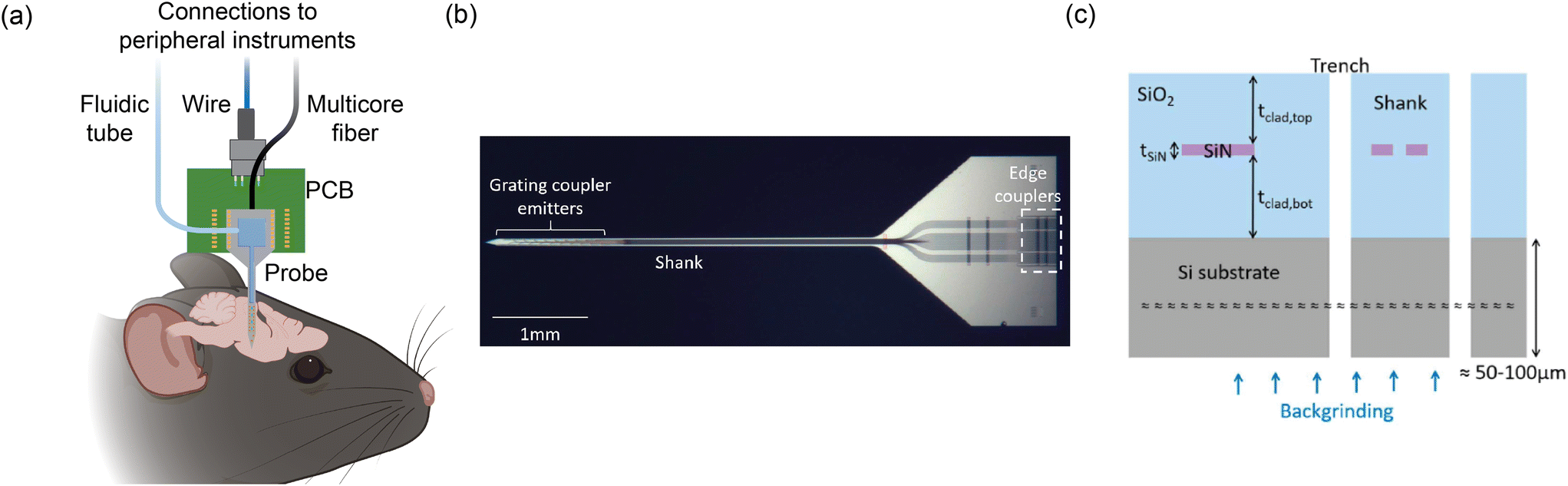 | ||
| Fig. 1 (a) Conceptual illustration of the multifunctional nanophotonic neural probe with its shank implanted in the mouse brain. Multiple devices can be integrated on the probe shank, including electrodes, optical emitters, and a 3D-printed microfluidic channel. Peripheral instruments are essential for enabling the probe to perform multichannel optogenetic stimulation, electrophysiological recording, and chemical delivery and sampling (see sections 3 and 4 for more details). The figure is created with https://BioRender.com. (b) Micrograph of a photonic-only nanophotonic neural probe featuring a single shank with 21 grating coupler emitters, each connected to an edge coupler on the chip facet of the probe base. (c) Cross-sectional illustration of the nanophotonic neural probe. A single SiN waveguide was used to form the passive visible photonic integrated circuits (PICs), mainly for routing light on the chip. The outline of the probe was defined by a deep trench process, and the probe was released from the wafer by backgrinding the Si substrate to a thickness of 50–100 μm. (b) and (c) are reprinted with permission from ref. 46 © Optical Society of America. | ||
2.1 Waveguides and routing components
Nanophotonic neural probes to date45–52,57–64 use SiN and SiO2 as the core and cladding of the waveguide, respectively, due to their optical transparency in the visible spectrum and compatibility with Si photonic foundries.46,67 The waveguide propagation loss is typically dominated by scattering from the sidewall roughness, quantified by the root mean squared of the roughness profile.68 Due to the high confinement of the optical field in the waveguide, short (blue) wavelengths require smoother sidewalls to achieve low propagation loss compared to infrared light. The SiN layer can be formed with either plasma-enhanced chemical vapor deposition (PECVD) or low-pressure chemical vapor deposition (LPCVD). PECVD SiN is formed at temperatures <400 °C, compatible with back-end-of-line (BEOL) processes in the foundry. The high temperatures for LPCVD SiN can anneal the waveguide material to reduce optical absorption.69 The PECVD SiN waveguides in our photonic platform, with cross-sectional dimensions of 340 × 135 nm2, were SM and had propagation loss between 6 and 1.5 dB cm−1 in the wavelength range of 430–648 nm,46 within the range achieved by other nanophotonic neural probes.45,60–62,64Light from a fiber-coupled external laser diode is coupled onto the chip using a fiber-to-chip edge coupler. We chose an edge coupler, instead of a surface grating coupler geometry, to minimize the physical profile of the device and to make it easier to fit under a microscope objective lens. The edge coupler is a waveguide taper with a width of 5.2 μm at the chip facet that narrows to the width of the routing waveguide over a distance of ∼400 μm. Nonetheless, due to the large mode mismatch between the fiber mode (∼3 μm) and the waveguide mode that is tightly confined in waveguides with thicknesses of 120–200 nm, most of the optical loss of the probe occurs at the chip facet with coupling efficiency of the edge coupler ranging from −6.9 to −11.3 dB for λ = 430–648 nm.46 For long, millimeter-scale routing distances from the probe base to the tip of the shank, we used waveguide widths in the range of 0.6–1 μm to reduce propagation loss due to sidewall roughness. Each waveguide is connected to a grating coupler emitter on the shank to radiate light vertically out of the probe.
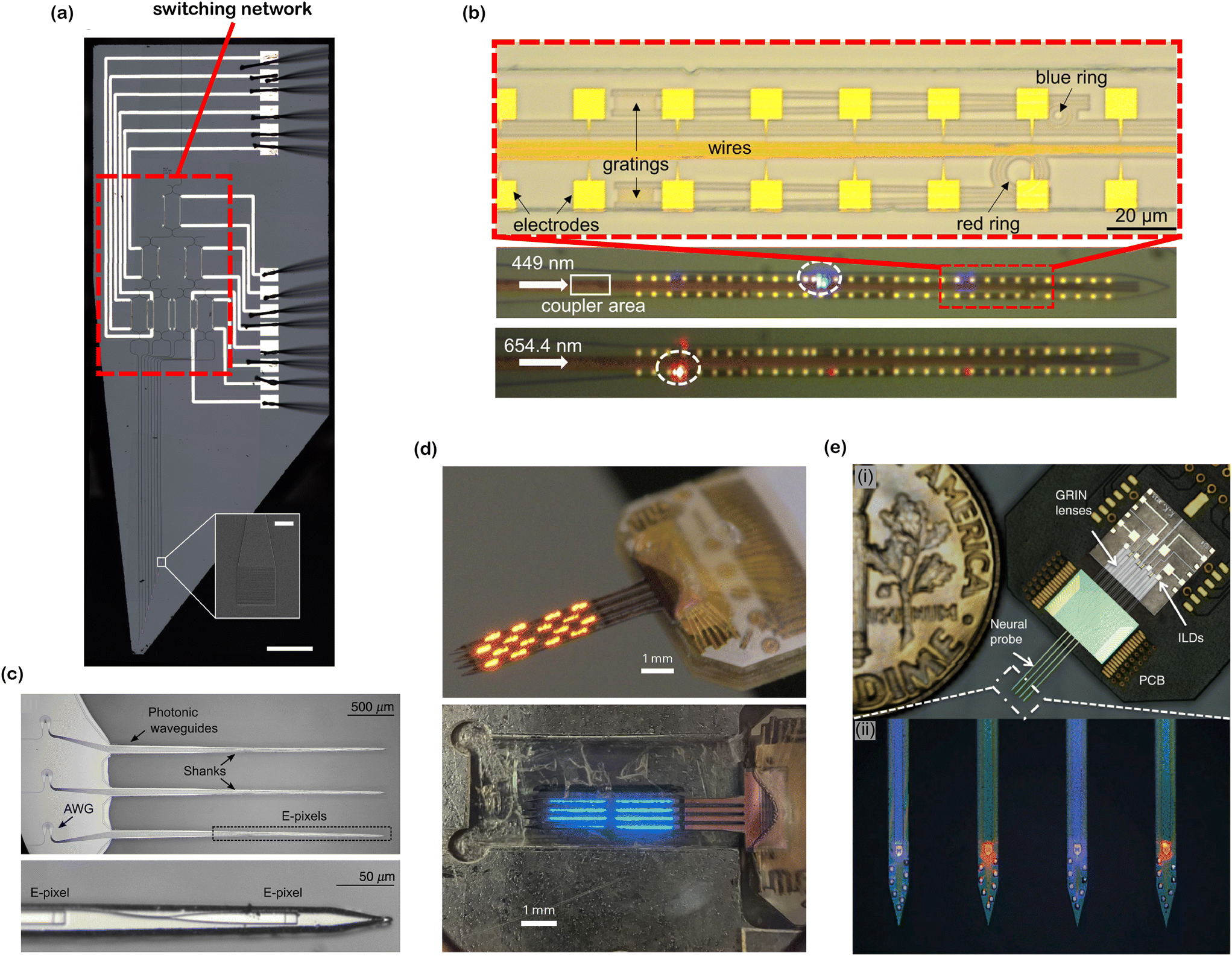
Complex optical routing, such as the routing network for light-sheet generation on the probe discussed in section 2.2.3, uses multimode interference (MMI)-based waveguide crossing structures and 1 × 2 power splitters. These devices exploit the self-imaging property within a MM waveguide, where the input field is replicated in single or multiple images at periodic intervals along the propagation direction.70 An output waveguide can be placed at the self-imaging positions to extract a replica of the input field. For the crossing structure in Fig. 2(a), the center of the crossing is located at the first self-imaging location where the converging beam pattern minimizes the scattering at the crossing. The output waveguide is located at the second self-imaging position to guide the light into a SM waveguide. For the MMI-based 1 × 2 splitter in Fig. 2(b), the two output waveguides are located at the two-fold self-imaging position to split the input power into two waveguides. Both devices are tolerant to fabrication variation because they do not contain fine feature sizes. They can operate in the visible spectrum (450–640 nm) with an optical loss of <3 dB and <1 dB at the designed wavelength.46 The loss of the device can be optimized for the excitation wavelengths of numerous opsins (i.e., ChR2, Halorhodopsin and ChrimsonR18,71,72) and indicators for functional imaging (i.e., GCamP6, jRGECO1 (ref. 9)).
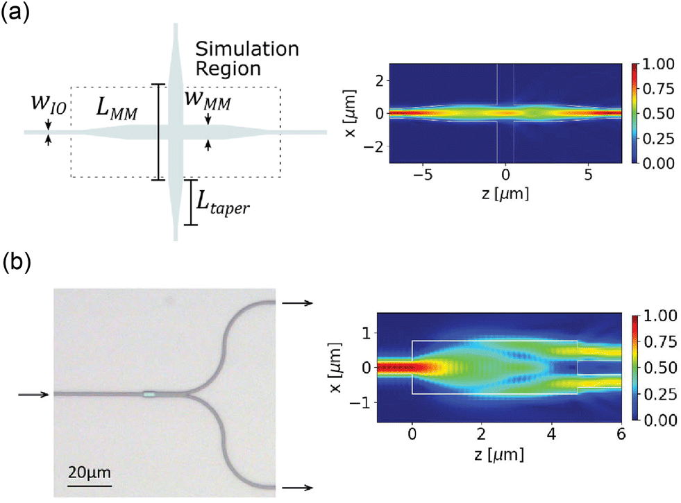 | ||
| Fig. 2 (a) Schematic of the waveguide crossing device and (b) optical micrograph of an MMI-based 1 by 2 power splitter. The simulated top-down electric field profile (|Ex|) for (a) and the electric field intensity profile (|Ex|2) for (b) are presented on the right. Reprinted with permission from ref. 46 © Optical Society of America. | ||
2.2 Grating emitters
The emitters used for optogenetic applications should meet the following three criteria. First, to induce robust spiking activity, the emitters should provide output power exceeding the intensity threshold of the opsins. For ChR2, the intensity threshold is about 1 mW mm−2.73 Second, the emitters should dissipate minimal heat with a conservative threshold of a 1 °C temperature increase in tissue to prevent thermally induced neuronal activity or tissue damage.74,75 Third, as an implantable device, the footprint of the emitter should be small enough to fit on the probe shank (ideally <60 μm in width to reduce tissue damage76).For nanophotonic neural probes with optical losses of 20–35 dB, grating emitters can induce robust stimulation with an output power of a few microwatts, as demonstrated in several studies.52,59–61,64 Moreover, these devices generally satisfy the thermal criterion because the main heat sources (i.e., light sources) are not in contact with the tissue. One distinct advantage of nanophotonic neural probes with SiN SM waveguides, in comparison with other Si-based implantable light delivery devices (i.e., optoelectronic Si probes, and probes with MM waveguides), is the versatility of their grating emitter design. The beam emission profiles of an emitter can be tailored to suit specific neuroscience applications and control the photostimulation extent. So far, four types of emitter designs have been realized on nanophotonic neural probes: (1) low-divergence uniform grating emitters, (2) out-of-plane focusing grating emitters, (3) light-sheet emitters, and (4) optical phased arrays. Most emitter types are small enough to fit multiples of them on a probe shank with width <100 μm (more details in the following subsections).
 | (1) |
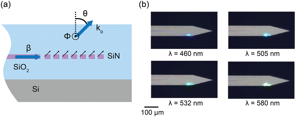 | ||
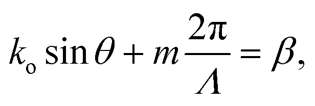
| Fig. 3 (a) 2D cross-sectional illustration of the uniform grating emitter structure. β is the propagation constant in the grating. The black arrows denote the light radiation from the incident beam in the waveguide on the grating structure. These radiated beams constructively interfere to form a directional beam with a wavevector ko and an emission angle of θ. ϕ represents the angular direction perpendicular to the plane. (b) Optical micrographs of the nanophotonic neural probe tip showing light emission at wavelengths of 460 nm, 505 nm, 532 nm, and 580 nm from a grating emitter. Adapted with permission from ref. 46 © Optical Society of America. | ||
The low-divergence gratings on our neural probes typically have a uniform grating pitch of 440 nm and a grating width of 6 μm and a length of about 30 μm, resulting in an emission angle close to 30° in air for blue light (λ = 488 nm) and beam divergence angles of <1.6° and <8° in θ and ϕ for λ = 430–645 nm,46 diverging less than the beam emission from LEDs and MM waveguides.28,38,42ϕ is in the direction out of the plane in Fig. 3(a), orthogonal to the θ direction.
Beam profiles are often characterized in fluorescein solution. The low-divergence grating designs can achieve a full-width at half maximum (FWHM) beam width of ≈10 μm at 100 μm distance.52,64 The emitter, shown in Fig. 3(b), also supports wavelengths of 430–645 nm with variations in emission efficiency and emission angle of about 10 dB and 30°, respectively. When operating the device at the optimal polarization for each wavelength, the total transmission loss from the edge coupler to the uniform grating emitter before fiber packaging can be > −18 dB,46 providing sufficient power budget for optogenetically inducing spikes which only require a few microwatts of output power. Overall, this broadband attribute is useful in experiments using multiple wavelengths to control different neuronal populations (e.g., using both ChR2 and ChrimsonR together).41
The designed grating pitch can diffract a second-order beam, but its intensity is >8 dB lower than the first-order beam over a wavelength span of 470–495 nm and 530–540 nm, with maximum suppression of 17 dB and 14 dB measured over these wavelength ranges, respectively.46 In terms of integration density, we can integrate 21 uniform grating emitters with a single SiN layer on a shank with width tapering from 90 to 72 μm, while achieving minimal waveguide crosstalk, similar to the large-scale μ-LED probes (32 μ-LEDs on a shank with width tapering from 140 to 50 μm (ref. 31)). Despite the sufficient shank space to integrate more emitters, the primary constraint to increase the number of emitters is the multiplexing scheme. So far, no nanophotonic neural probes have demonstrated more than 16 channels per multiplexer,45,59–61,64 possibly due to design considerations on optical loss and channel crosstalk.59,60 Further optimization of device performance in visible wavelengths is required to scale the channel count. Another solution to increase the number of addressable channels is to use multiple multiplexing schemes (see section 5.2.3).
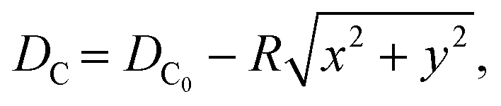
A schematic of this type of emitter is shown in Fig. 4(a). The grating teeth of the emitters are defined in the x–y plane based on a phase-matching condition adapted from ref. 81 for a radial incident phase profile and a spherical output phase profile centered at the focal site, (x0, y0, z0). The phase-matching condition is
 | (2) |
 | (3) |
 | ||
| Fig. 4 (a) Schematic of the out-of-plane focusing grating emitter with focal location (x0, y0, z0). (b) Phase map generated by summation of the incident phase profile and output phase profile over the x–y plane. The contour lines satisfying the phase-matching condition are overlaid in green. (c) Simulated beam emission profile on the y = 0 plane. (d) Emitted beam cross-section (x–y plane) captured at various heights (z-axis) above the surface of the probe immersed in water. (e) Captured side profile (x–z plane) of the beam emitted from an out-of-plane focusing grating emitter on a probe implanted near the surface of a fixed brain tissue with Thy1-GCaMP6s expression. The red line indicates the axis of narrowest beam width over which the beam waist is measured. Reprinted with permission from ref. 51. | ||
In ref. 51, we demonstrated this concept in a neural probe. The focal height was established at z0 = 50 μm, with the parameters x0 and R optimized through two-dimensional (2D) finite-difference time-domain (FDTD) simulations on the y = 0 plane. Subsequent validation was achieved using a 3D FDTD simulation, as illustrated in Fig. 4(c). The optimized grating was designed for λ = 488 nm for ChR2. The grating was 20 μm × 60 μm in size, allowing for the integration of 16 emitters on a 6 mm long, ∼100 μm wide shank.
The focusing capability of these probes in water and tissue was characterized (for details, see ref. 51). The cross sections of the emitted beam in water over the x–y plane are depicted in Fig. 4(d). The measured beam waist had a width of 4.0 μm × 4.3 μm (FWHM). Due to the long grating periods present in the emitter, higher diffraction orders were present as shown in Fig. 4(d). The intensity of the unwanted diffraction orders was >7 dB lower than the focal spot intensity in the imaged beam cross-sections, which would be sufficient to suppress unwanted ChR2 activations.82
Next, we report the first demonstration of focusing of light on biological tissue from a grating emitter. The fluorescence emission profile was captured in a fixed brain slice expressing Thy1-GCaMP6s, as shown in Fig. 4(e). The focal point beam width in the tissue was about 8.4 μm (FWHM) measured along the red line in Fig. 4(e). This beam width roughly matches the diameter of the neuronal soma,83 and can be further combined with optogenetic actuators that target expression in specific structures of neurons84 for spatially precise optogenetic stimulation.
Ref. 47 reported the synthesis of a light sheet using a set of grating emitters with a large divergence angle in ϕ, which allows the emission from neighboring gratings to merge and form a sheet. The dimensions of the grating were 1.5 μm × ∼28 μm to achieve a wider divergence angle in ϕ while maintaining a narrow divergence angle in θ. The optical input to an edge coupler was split into 4 or 8 gratings on the shanks with a routing network consisting of 1 × 2 power dividers and waveguide crossings, as shown in Fig. 5(a). The light-sheet beam profile in fluorescein solution had a semi-uniform beam region covering an area >0.22 mm2 and an FWHM sheet thickness of <16 μm up to 300 μm propagation distance in free space, slightly larger than the sheet thickness realized with another neural probe implemented with a single grating as the light-sheet emitter.92 Optical sectioning in imaging could be achieved by sequentially addressing light to the 5 light-sheet emitters on the shanks with a vertical pitch of 78 μm. Each shank tip had a width of 60 μm and a thickness of 50–92 μm.
 | ||
| Fig. 5 (a) Illustration of light-sheet formation using an array of four grating emitters. Light, coupled to a single edge coupler, is split across the shanks via the routing network depicted in the schematic on the right. (b) Demonstration of light-sheet calcium imaging in a brain slice from a Thy1-GCaMP6s mouse, with the light-sheet illumination from the probe. The fluorescence time trace on the right reveals activity in multiple neurons within the region of interest labeled in the fluorescence image. The scale bar in the fluorescence microscopy image is 50 μm. (a) and (b) are reprinted from ref. 47 under a Creative Commons CC-BY 4.0 license. (c) Schematic of the light-sheet light-field microendoscope, implemented through a fiber bundle attached to the light-sheet probe. Images of the assembled device are on the right. Reprinted with permission from ref. 85. (d) Comparison of the volumetric image of fluorescent beads suspended in agarose, reconstructed using the light-field images with epi-illumination via a fiber bundle and light-sheet illumination. The volumetric reconstruction using light-sheet illumination achieves superior imaging depth with a higher signal-to-noise ratio (SNR) due to optical sectioning. The reconstructed volumes from epi-illumination and light-sheet illumination have dimensions of 512 × 512 × 200 μm and 512 × 512 × 250 μm (xyz), respectively. Z axes were stretched for both volumes for visualization. Reprinted from ref. 86 under a Creative Commons CC-BY 4.0 license. | ||
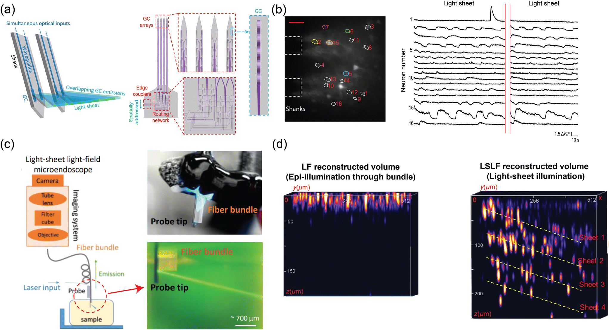
The light-sheet probe was used for LSFM and light-field microendoscope imaging.47,86 Using the probe as the illumination for LSFM,47 the fluorescence was collected using a long working distance objective from a fixed tissue, an ex vivo GCaMP6 brain slice, and the cortex in vivo. Light-sheet illumination significantly improved image contrast in fixed tissue imaging, achieving over a 3-fold increase in the regions of interest (ROI) with neurons compared to epi-illumination. For the ex vivo brain slice experiment, Fig. 5(b) shows that light-sheet illumination had sufficient and stable power to allow clear observation of calcium dynamics. At the peak of the calcium events, 4 out of 5 neurons showed enhanced image contrast compared to epi-illumination detailed in ref. 47. The probe has also been attached to a fiber bundle light-field microendoscope to reduce the form factor of an implantable imaging system and to eliminate the need for an adjustable focus.86Fig. 5(c) shows the light-sheet light-field (LSLF) microendoscope with a light-sheet probe attached to a 650 μm-diameter imaging fiber bundle. The fiber bundle encodes the angular information of light rays in the optical modes of individual fiber cores for the light-field reconstruction. The algorithm in ref. 93 was used to reconstruct the volumetric image. The light-sheet illumination reduces the background signal and provides a sparser signal with optical sectioning compared to epi-illumination; thus, the LSLF microendoscope achieved a significant enhancement in image contrast and noise reduction especially at image depths >50 μm. This enhancement is shown in the volumetric images of an agarose block with fluorescent beads in Fig. 5(d).
These examples show that the light-sheet neural probe opens a new approach to realize LSFM in a small form factor suitable for freely behaving animal experiments. The combined dimension of the probe and the fiber bundle is around 750 μm thick, smaller than the GRIN lens approach, which is around 2 mm thick.91 Although the light sheet emitted from the neural probes is currently thicker than the sheet formed with lenses (16 μm vs. <10 μm), optimizing the grating pitch can generate a more focused beam along the axis of sheet thickness.57 Beyond applications in LSFM imaging, light-sheet neural probes are also useful for selective laminar optogenetic stimulation, enabling optically sectioned interrogation of layers within a brain region.
Neural probes with integrated SiN optical phased arrays (OPAs) can meet these requirements. OPAs are solid-state devices that utilize an array of coherent emitters to perform beam shaping and steering.99–101 By adjusting the phase relationships among the emitters, OPAs can create a directional beam in the far-field via interference, and the beam can be dynamically steered by updating the phase relationships between the emitters. In the case of a one-dimensional array of optical emitters, the emission angle of the main beam in ϕ is given by102
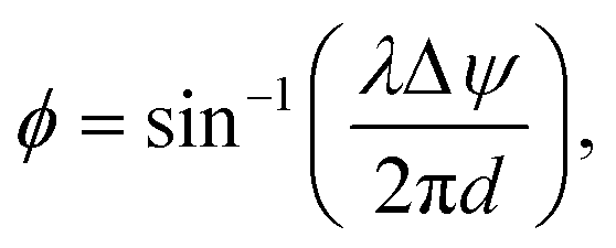 | (4) |
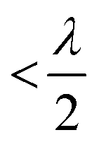 to achieve single-lobe emission. However, achieving such close emitter spacings at visible wavelengths is challenging due to fabrication limits and inter-waveguide crosstalk.103 Innovative strategies, like using an aperiodic pitch OPA103 or on-chip microelectromechanical system (MEMS)-based devices,104 can enable a single steerable beam at visible wavelengths without satisfying the
 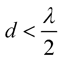 criterion. However, due to factors like their size, thermally tuned phase shifters, or mechanical actuators near the light emitter, these approaches are not ideally suited for implantable neural probes, as they could potentially damage the tissue.
Fig. 6(a) shows the first OPA design integrated onto a neural probe.48 The OPA design was adapted from ref. 105 for blue wavelengths. The OPA was passive; the differential phase shift between light emitters in the OPA was varied by tuning the input wavelength. This wavelength tuning range was designed to be within the excitation spectrum of ChR2 and GCaMP6. The OPA comprised a star coupler, which divided input laser light into 16 delay line waveguides with a differential path length difference of 16 μm for a free spectral range of 6 nm. Each delay line terminated in a grating coupler with a period of 440 nm and a fill factor of 50%. The grating couplers formed a 1D optical phased array with an array pitch of 700 nm.
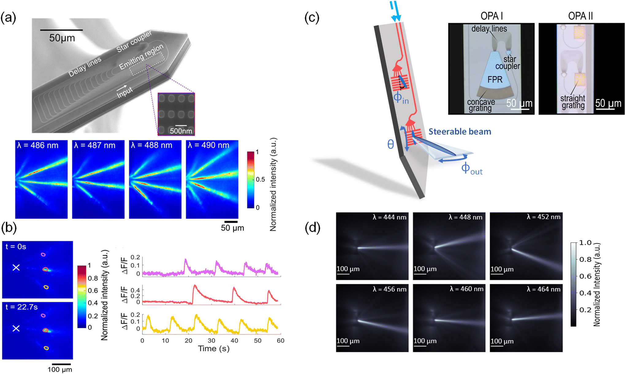 | ||
| Fig. 6 (a) Scanning electron micrograph of an optical phased array (OPA) on a neural probe. The inset is a portion of the SiN grating array before the top cladding was deposited during fabrication. Below are the measured top-down intensity beam profiles of the OPA emission in a brain slice from a VGAT-ChR2-EYFP mouse.48 (b) Functional imaging test of the OPA neural probe in (a). Top-down fluorescence images at times t = 0 s and t = 22.7 s show high contrast time-dependent fluorescence changes in the regions of interest. (a) and (b) are reprinted with permission from ref. 48 © Optical Society of America. (c) Two different sidelobe-free optical phased array designs integrated on neural probes. The use of a slab-grating emitter enables single beam emission.49,50 Compared to OPA I, OPA II contained no free propagation region (FPR) slab and employed a straight instead of curved grating. (d) Top-down intensity beam profiles at various wavelengths of OPA II in (c) when immersed in a fluorescein solution.50 (c) and (d) are adapted with permission from ref. 49 and 50. | ||
The steerable light beams from OPA probes were captured using fluorescence microscopy of the yellow fluorescent protein (YFP) in cerebellum slices of VGAT-ChR2-EYFP mice as shown in Fig. 6(a). The presence of three steerable beams is attributed to the array pitch (700 nm), which exceeds the half-wavelength criterion required for single-lobe emission. Over the wavelength range from 486 to 490 nm, as the emitted beams propagated 50–150 μm away from the neural probe, the beam width remained <23 μm (FWHM). In the hippocampal brain slices from Thy1-GCaMP6s mice, the OPA probe illuminated three neurons or clusters of neurons as shown in Fig. 6(b), and spontaneous time-dependent fluorescence was imaged with high contrast. The rise and fall times of the calcium events corresponded to the GCamP6s dynamics for the burst of spikes. The OPA was also used for optogenetic stimulation of the brain slices on a microelectrode array.48
To emit a single beam without satisfying the half-wavelength criterion, an alternative OPA approach is to steer the beam in the plane of the probe with an end-fire OPA in a structure that removes the side lobes and then emits the light out of the probe with a grating. “End-fire” refers to a configuration where light is emitted in the plane of the probe. Fig. 6(c) from ref. 49 shows an example of this approach. In this OPA design (OPA I), the waveguide delay lines were brought to a 400 nm pitch forming an in-plane OPA that emitted light into a 100 μm-long free-propagation slab region (FPR). In the FPR, the higher-order beams do not reach the grating region at the end of the slab for out-of-plane emission. Tuning the input wavelength steers the beam in the FPR which results in a lateral translation in the beam position. The steering is further contributed by the dependence of the output coupling angles (ϕout) on the incident angle (ϕin) of the slab beam. The angles ϕin and ϕout are depicted in Fig. 6(c). In fluorescein solution, a single lobe was steered over a lateral distance of 57 μm at a distance of 100 μm away from the OPA. Although the OPA in ref. 49 demonstrated sidelobe-free steering, the device was limited by its large footprint, which required a neural probe with a shank width of 154 μm.
The approach can be miniaturized by coupling the end-fire OPA directly into a straight 1D grating and removing the FPR as shown in OPA II in Fig. 6(c).50 This design reduces the OPA size by 2.5 times and can be integrated on a 100 μm-wide shank. Furthermore, by replacing the curved grating with a straight grating, the steering range is ≈1.4× wider 100 μm away from the OPA compared to OPA I. The steering range improves because a straight grating changes the relationship between the incident angle (ϕin) of the OPA emission and the output coupling angle (ϕout), as explained by the phase matching condition presented in ref. 106. Within the wavelength tuning range of 444 nm to 464 nm, the FWHM beam width of OPA II was ≈20–30 μm, and the beam could be steered laterally over 78 μm at a distance of 100 μm (Fig. 6(d)). The peak beam intensity was 6–7 dB greater than the background intensity for input wavelengths of 444 nm and within the 456–464 nm range, limited by scattered light from the PIC. At the limits of the steering range (i.e. λ = 448 nm, 452 nm), the side-lobe suppression ratio was reduced to 4.7 dB, due to aliasing. Moving forward, the sidelobe-free OPAs should aim to further reduce the device size, extend the beam-steering range, improve the side-lobe suppression ratio, and increase the scanning speed for fast, spatially selective photostimulation.
3 Multi-modal neural probes
In the previous section, we described neural probes that only emit light. To fully capture the activity of neurons, it is essential to stimulate and record in multiple modalities. The gold standard for monitoring cellular activity is electrophysiological recordings, which can be accomplished by recording extracellular electrical spiking activity with surface electrodes integrated on implantable devices.107 Combining pharmacological modulation and cell-type-specific optogenetic stimulation also provides an effective approach for dissecting neural circuits.42,108,109 The wafer-scale Si photonic technology can support the integration of multiple functionalities into a single probe. In this section, we will discuss the integration of (1) microelectrode arrays for electrophysiological recording and (2) 3D-printed microfluidic channels for neurochemical delivery onto the probes. Fig. 7(a) illustrates the cross-section of a multimodal neural probe, which includes optical waveguides for light delivery, surface electrodes for electrophysiology, and a microfluidic channel for chemical stimulation and sampling.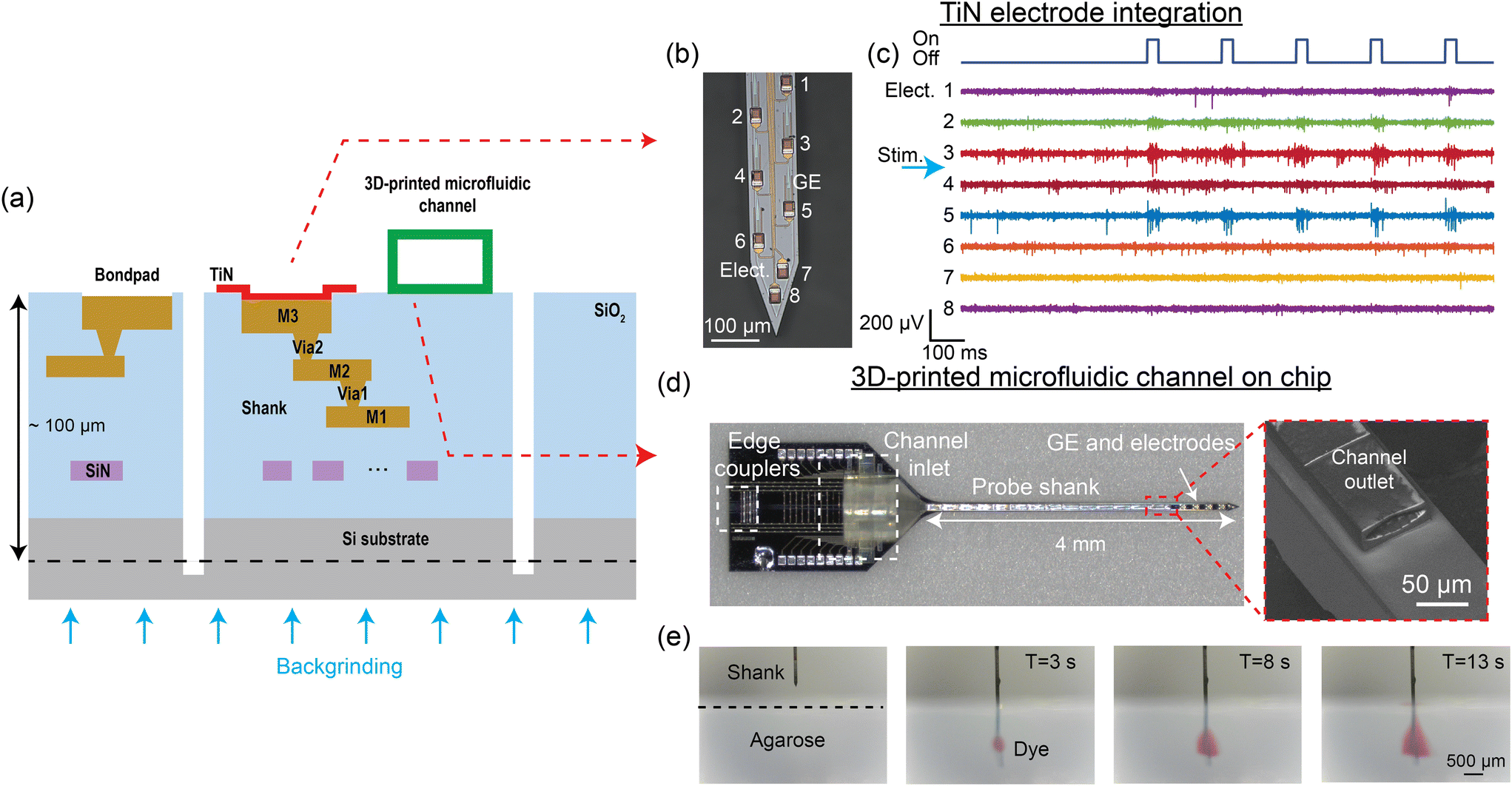 | ||
| Fig. 7 (a) Cross-sectional illustration of the multi-modal neural probe. In addition to the single SiN waveguide layer, 3 metal routing layers and TiN surface electrodes are integrated to realize electrophysiological recording with the probe.52,55 Microfluidic channels can also be printed on the probe, allowing neurochemical drug delivery to the brain.56 (b) Micrograph of the neural probe shank with TiN electrodes (Elect.) and grating emitters (GE). The numbers indicate the electrode channel index. (c) A 1.4 s snapshot of electrophysiological recordings from the 8 electrodes at the tip of the shank (matching channel index in (b)) performed in an awake head-fixed experiment with a Thy1-ChR2 mouse. A pulse train of 30 ms optical pulses was delivered from an emitter on the shank for optogenetic stimulation, leading to an increase in spiking activity, notably on Elect. 3 and 5. The position of the stimulation emitter is indicated with the blue arrow between Elect. 3 and 4. (d) Neural probe with a 3D-printed microfluidic channel, with the inset showing the scanning electron micrograph of the channel outlet on the probe shank. (e) Front-view sequential photographs of red dye diffusion in an agarose gel. (d) and (e) are reprinted from ref. 56 under a Creative Commons CC-BY 4.0 license. | ||
3.1 Integration of TiN microelectrodes
Implantable devices that combine optogenetic stimulation and electrophysiological recording capabilities are used for studying the roles of specific cell types in the brain.25,110 For electrophysiological recordings, multi-site surface microelectrodes can be integrated on Si probes to spatially sample extracellular activity across the targeted brain regions. The microelectrode material should be biocompatible to minimize tissue responses.111 In addition, microelectrodes for detecting single-unit activity require low impedance (<2 MΩ at 1 kHz)112 and small size (<32 × 32 μm2)113 for an optimal signal-to-noise ratio and minimal signal attenuation. Currently, numerous electrode materials, including gold, platinum, and titanium nitride (TiN), have been successfully integrated on nanophotonic neural probes with an electrode count typically below 100 sites.52,59–61,63 These electrodes meet the biocompatibility, impedance, and size requirements, with the choice of material largely dependent on the fabrication process.In ref. 52 and 55, surface recording electrodes were integrated with our nanophotonic neural probes by introducing 3 aluminum (Al) layers for electrical routing and a TiN layer on the chip surface as shown in Fig. 7(a). TiN was used because it is compatible with CMOS fabrication. Each electrode was connected to a bond pad on the probe base, and the measured signal was amplified and digitized off-chip with an Intan amplifier headstage. Fig. 7(b) shows TiN electrodes and low-divergence grating emitters on the shank of a neural probe. This particular probe design had 18 TiN electrodes, each 20 μm wide, and 16 optical emitters that spanned ≈1 mm along the shank. We have also realized probes with a total of 72 electrodes distributed across 4 shanks. Different emitter designs, presented in section 2.2, can be implemented with an electrode placement suited for the beam emission profile. The as-fabricated 20 μm-wide TiN electrodes had an impedance of 4–6 MΩ at 1 kHz. Methods to reduce the impedance of the electrodes <2 MΩ include immersion in a hydrochloric acid bath114 and electrode roughening with a femtosecond laser.52,115 The noise level of the electrical recording measured with laser-roughened 20 μm electrodes in 1× phosphate-buffered saline (PBS) solution was 4.2 ± 0.23 μV (root mean squared).52
Fig. 7(c) shows an example recording from layers V and VI in the motor and somatosensory cortex of an awake head-fixed Thy1-ChR2 mouse from a probe with nanophotonic waveguides and TiN electrodes. The optical pulse train stimulation had a pulse width of 30 ms at a frequency of 5 Hz. The increase in spiking activity recorded by electrode channels 3 and 5 during the optical pulses confirmed that the probe emitted sufficient power to activate the ChR2. Integrating TiN surface electrodes with grating emitters on the nanophotonic neural probe enables simultaneous electrophysiological recording and optogenetic stimulation with a single implant. Scaling the electrode density, so that the spiking activity of a neuron can be oversampled on multiple electrodes, will improve the accuracy of spike sorting and cell type classification.16,17
3.2 3D-printed microfluidic channels
The delivery and sampling of neurochemicals are used to study complex neural circuits and have significant potential in the treatment of neurodegenerative diseases.116–122 An approach to integrate microfluidic channels onto foundry-fabricated probes is to use 3D printing or laser writing.56,123 A neural probe with a microfluidic channel written via two-photon polymerization is shown in Fig. 7(d). The overall thickness of the probe was ∼100 μm. The neural probe consisted of a base (1.7 mm × 2.7 mm) and a 4 mm long probe shank, with 4 low-divergence grating emitters near the tip of the probe shank. The 3D-printed microfluidic channel on the probe had a length of 4.3 mm, with the channel inlet/outlet located on the probe base/shank. The outer dimensions of the printed channel on the shank were 80 μm in width and 30 μm in height; the inner dimensions were 70 μm in width and 18 μm in height. A 1 mm long fluidic connector with a 750 μm inlet diameter printed on the probe base facilitated coupling to an input fluidic tube. Fig. 7(e) shows sequential photographs of the injection of red dye from the probe into a 1% w/v agarose gel block. The flow rate was linearly dependent on the inlet pressure, and the channel remained intact for more than 10 weeks immersed in artificial cerebrospinal fluid. As a proof-of-concept application, the probes were used to uncage CMNB-caged fluorescein in solution and fixed brain tissue.56 The photolysis of CMNB-caged fluorescein was achieved using λ = 405 nm light from the grating emitter, allowing for localized uncaging in brain tissues. The 3D-printed microfluidics offers high flexibility in fluidic channel design and enables the Si neural probes to have photonic, electrophysiological, and microfluidic capabilities.4 Packaging and system integration
The nanophotonic probe chips discussed so far are part of a system that is illustrated in Fig. 8. Since the probes are passive, light is coupled onto the chip from an external laser. Each grating emitter on the probe is connected to an on-chip edge coupler, which is aligned to one of the cores of a custom multi-core fiber (MCF).124 The MCF has up to 16 cores in a linear arrangement, and each core is SM across the visible spectrum with low inter-core crosstalk, particularly at the blue wavelengths (≤-35 dB in 1 m). The light from an external laser is deflected to each core in the MCF using a MEMS mirror-based laser scanning system.47,48 The compact scanning system shown in Fig. 8(a) has a footprint of approximately 30 × 30 cm2, smaller than the system in ref. 47 and 48, and includes a depolarizer (to reduce power fluctuations due to polarization drift) and optical power monitoring for feedback. With this scanning system, the variation in probe output power can achieve <10% for at least 2 hours.55 The scanning system needs to be realigned for different input wavelengths (i.e., blue and red) due to chromatic focus shifts, and including a diffractive optical element can reduce this shift to support the simultaneous use of multiple wavelengths.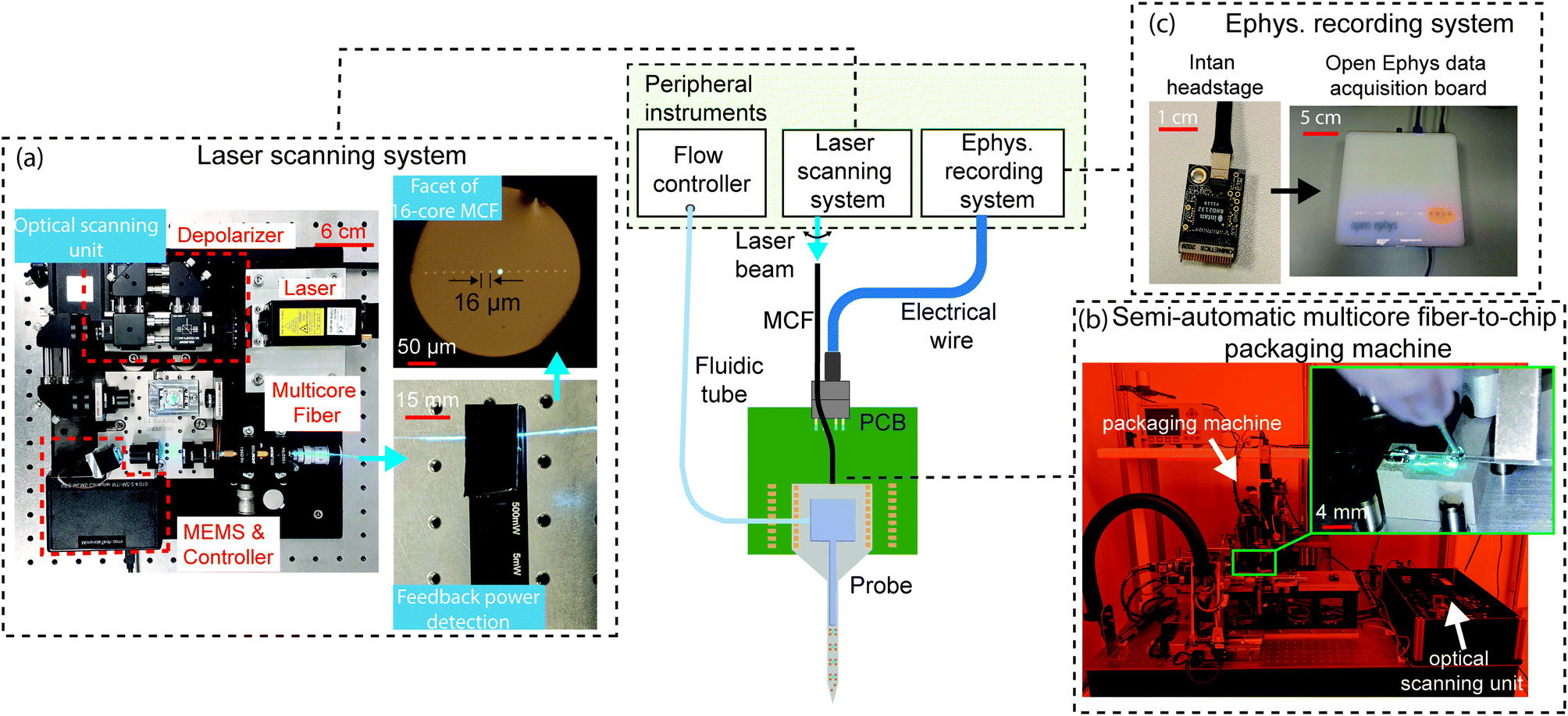 | ||
| Fig. 8 The central image is the system diagram of the nanophotonic neural probe and its peripheral instruments, facilitating optogenetic stimulation, electrophysiological recording, and chemical delivery and sampling. A laser scanning system addresses light to emitters on the probe via a multicore fiber (MCF), an electrophysiology (ephys.) recording system detects electrical signals from the on-chip electrodes, and a flow controller delivers or samples chemicals through the 3D-printed microfluidic channel. (a) Photographs of the compact MEMS-based scanning unit for addressing light to individual cores on the 16-core MCF. A feedback photodetector was attached to the MCF to assist in fine-tuning the alignment between the optical scanning unit and the MCF. (b) Photographs of the semi-automatic packaging machine for the MCF-to-chip attachment process. The inset shows the epoxy application procedure for the attachment of the MCF to the chip. (c) Multichannel electrophysiological recordings through the TiN electrodes on the chip are acquired using the Intan headstage and Open Ephys data acquisition system. Adapted with permission from ref. 55. | ||
The MCF is attached to the probe using UV-curable epoxies, either manually or with a semi-automatic packaging system in Fig. 8(b). Due to the tight alignment tolerance between the fiber cores and the on-chip edge couplers, the epoxy is applied incrementally along the fiber and the probe to minimize shrinkage during curing. The thickness of the probe (∼50–100 μm) also limits the available bonding surface area between the MCF and the chip edge, which reduces the mechanical stability of the fiber-to-chip packaging and compromises the packaging yield.125 The semiautomatic packaging machine, co-developed with ficonTEC GmbH, actively aligns the MCF with the on-chip edge couplers and precisely controls the epoxy application and curing. The output power variation across the emitters on the probe packaged with the machine was within 5.3 dB for 3 packaged probes.55 To reduce the optical insertion loss caused by the misalignment of the MCF-to-chip interface during packaging, the probe shanks can be selectively thinned to preserve a thicker base for the edge couplers,64 and a V-groove can be cut in the probe holders to increase the fiber attachment stability. Using grating couplers instead of edge couplers can improve packaging reliability due to larger bonding surface area and greater tolerance for displacement caused by epoxy shrinkage.125 However, for applications requiring simultaneous imaging and probe implantation, the fiber-to-grating coupler packaging will make the probe base thicker, potentially causing clearance issues with a microscope objective lens.
To support electrophysiological recording capabilities (see Fig. 8(c)), the probes are wirebonded to rigid or flexible PCBs, which are connected with Intan amplifier chips for signal amplification and digitization. The Open Ephys data acquisition board126 is used to interface the digitized neural signal and other external trigger signals with the computer. Although this method allows the electronic components to be reused, the amplifier circuit board would further increase in size and weight to support >128 recording channels and can be incompatible with freely moving animal experiments which require the device weight to be <3 g.127 Si probes adopting monolithically integrated active amplification and recording circuitry can scale to >5000 electrode sites while maintaining a small footprint for freely moving animal experiments.13 A modular approach is to use a Si interposer with high-density lithographically patterned traces.128 By bonding the probe and Intan amplifier dies to the interposer, this method can potentially support hundreds of recording channels in a compact form factor and offer the flexibility to mix and match electronic chips with a variety of probes.
5 Discussion and outlook
5.1 Challenges of nanophotonic neural probes
Although foundry-based wafer-scale technology offers significant advantages for large-scale device integration and high-volume fabrication, there are several challenges involved in neurotechnology development in foundries. One key constraint is material selection. For example, TiN is often used for surface electrodes in foundry-fabricated probes12,13,45,52 as it is compatible with CMOS fabrication. However, alternative transparent electrode materials such as PEDOT:PSS,32 which can realize higher electrode-to-emitter integration densities by placing electrodes directly above optical emitters without obstructing light emission, are not part of these standard processes. Another limitation is that foundries use Si as the device substrate, which exhibits a significant mechanical mismatch with brain tissue. This mismatch in mechanical properties can lead to adverse effects on tissue that ultimately compromise the stability of chronic recordings, due to (1) encapsulation of the implant by microglial and astrocyte cells from immune responses and (2) tissue damage caused by micromotion between the implant and the brain.132 In contrast, flexible implants made with polymers have superior long-term stability, with the record of monitoring single-unit activity over the lifespan of a mouse (∼18 months).133 In addition to material challenges, some fabrication processes are absent or not optimized for neural applications, necessitating post-processing steps, such as laser micromachining (see section 3.1) and 3D laser writing (see section 3.2), to achieve the desired functionality. Since these post-processing steps are not necessarily carried out at the wafer-scale, they can limit the manufacturing scalability. Overcoming these obstacles requires close collaboration with foundry partners to develop new compatible process steps. An example of efforts to reduce post-fabrication steps is the integration of microfluidics discussed in section 5.2.4.In addition to the limitations imposed by foundry fabrication, nanophotonic neural probes have not been widely deployed to neuroscience groups for functional brain mapping due to several challenges. First, the operation of the nanophotonic neural probes can be difficult for many users. Our probe, for example, requires alignment of the free-space optical scanning unit and the MCF to ensure stable optical power output for consistent stimulation responses. Similarly, probes employing wavelength division multiplexers or optical switches (section 5.2.3) necessitate calibration, like laser wavelength tuning or voltage bias optimization, to optically address specific emitters with minimum inter-emitter crosstalk,45,59,60,64 thereby preventing stimulation in unintended brain regions. Second, most probes suffer from high optical loss, ≳8 dB, at the fiber-to-chip coupling interface.45,52,57–59,62–64 The shrinkage of UV-epoxy during curing can further reduce the fiber-to-chip coupling efficiency.125 The long-term stability and reliability of the optical package remain an area for further study and improvement. The optical loss from the fiber-to-chip coupling can limit the power output from the probe, hindering its capability to output high power for stimulating large neuronal populations134 or to evaluate stimulated behavioral responses over a wide range of optical intensities.135 Third, studying brain activity in chronic, freely behaving animal experiments can offer valuable insights into the neural mechanisms of naturalistic behaviors, such as social interactions136 and decision-making.137 However, current in vivo demonstrations of nanophotonic neural probes are limited to acute, head-fixed experiments partly due to the lack of an optical connector on the probe for disconnecting the mouse from the fiber for post-surgery or experiment recovery. Furthermore, the need for fiber inputs and electrical wires on nanophotonic probes requires either additional cable design or a shift to wireless design to minimize the torque imposed on the animal, which can otherwise influence its behavior.138,139 While ref. 61 managed to replace the fiber input with a laser diode mounted on the probe, each laser diode mount was pre-aligned to illuminate only one grating emitter, and manual swapping of the mount was required to address light to other emitters.
5.2 Future directions
Some of the challenges of the nanophotonic neural probe can be improved at the component level and with active devices. By introducing devices like laser diodes and optical switches, we can realize probes with more optical emitters and eliminate the need for fiber inputs to address multiple emitters. Compared to optoelectronic neural probes, most of these active devices are outside the brain, on the probe base; thus, reducing the risk of tissue heating. We have successfully demonstrated devices such as photodetectors (PDs), thermo-optic switches, and MEMS devices on a photonic platform similar to those for neural probes.140 Our future neural probes can use these active devices to make the probes more user-friendly and suitable for chronic, freely behaving animal experiments. These active devices can also scale up the optical emitter count and extend the capabilities of the probes for on-chip biosensing applications with PDs. In the following subsections, we outline prospective avenues for improving our existing neural probe platform, transforming it into a versatile multifunctional device for brain interrogation.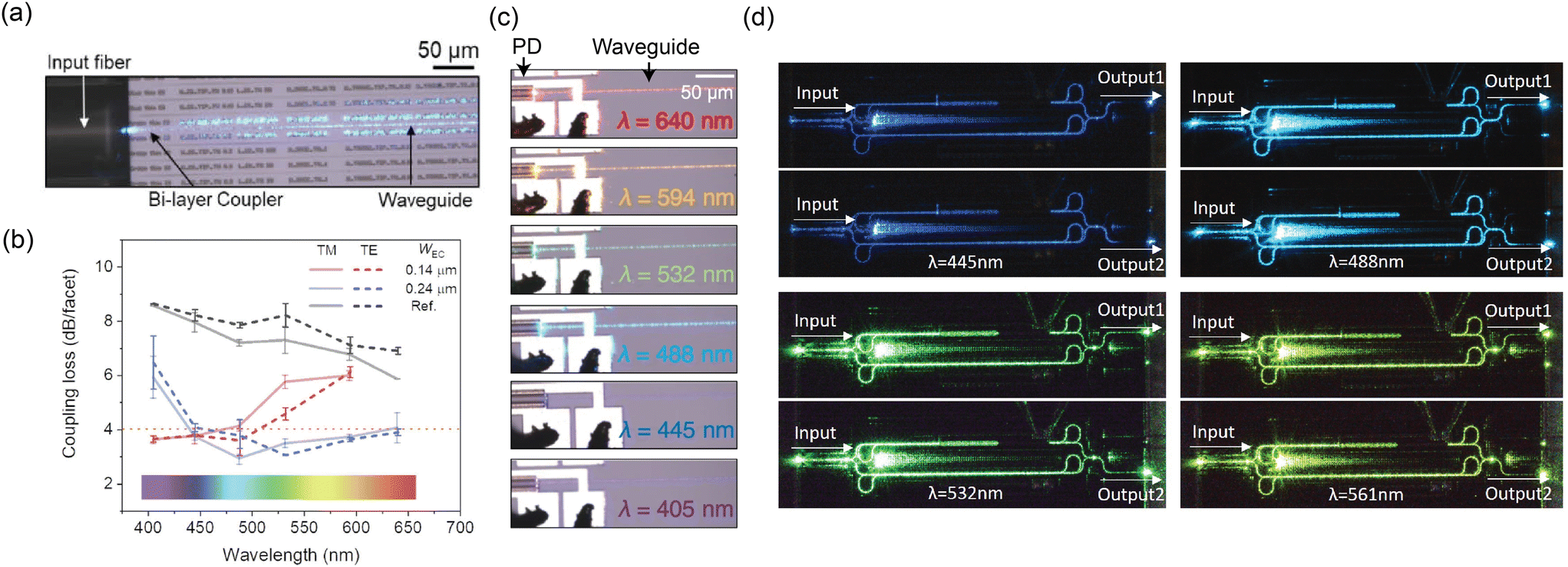 | ||
| Fig. 9 (a) Optical micrograph of the fiber input at λ = 488 nm coupling to a bi-layer edge coupler. (b) Comparison of coupling loss between the bi-layer edge couplers and a single-layer edge coupler reference design. The figure also shows the coupling losses of two bi-layer edge coupler designs with different tip widths at the chip facet (WEC). (a) and (b) are reprinted with permission from ref. 129 © Optical Society of America. (c) Optical micrographs of the SiN-on-Si PD with different input wavelengths. Reprinted from ref. 130 under a Creative Commons license. (d) Optical micrographs of the undercut phase shifter integrated into an MZI switch operated at various input wavelengths. The phase shifter allows selective routing of the input light to output 1 or 2 depending on the applied phase shift. Reprinted with permission from ref. 131 © Optica Publishing Group. | ||
 | ||
| Fig. 10 Various optoelectrode and photonic neural probe designs. (a) Reconfigurable nanophotonic neural probe with an on-chip cascaded thermo-optic MZI switching network (main image scale bar: 500 μm, inset image scale bar: 10 μm). Adapted from ref. 60 under a Creative Commons license. (b) Dual-color nanophotonic neural probe with a passive ring resonator for wavelength division multiplexing (WDM). Adapted from ref. 58. © IOP Publishing. Adapted with permission. All rights reserved. (c) 9-Channel nanophotonic neural probe with on-chip WDM using arrayed waveguide gratings (AWGs). Adapted from ref. 64 under a Creative Commons CC-BY 4.0 license. (d) Orange- and blue-color 1024-channel μ-OLED optoelectrodes. Reprinted from ref. 32 under a Creative Commons license. (e) Dual-color fiberless photonic neural probe with 8 integrated injection laser diodes. Inset (i) shows the assembled probe on a PCB and inset (ii) shows the magnified view of the probe shanks. Adapted from ref. 41 under a Creative Commons license. | ||
6 Conclusion
Wafer-scale fabrication processes in commercial foundries enable the scalable manufacturing of nanophotonic neural probes for widespread adoption of the technology within the neuroscience community. Nanophotonic circuits provide functionalities such as optical beam shaping, wavelength multiplexing, and detection, within micrometer to millimeter scale form factors, suitable for brain implants in mice. Electrophysiological electrodes and 3D-printed microfluidics can be integrated to create tools for multimodal brain interrogation. Operating these probes also requires peripheral systems and advanced device assembly or packaging methods. Looking ahead, the integration of components such as PDs, optical switches, laser diodes, and fluidic channels into nanophotonic neural probes should simplify the peripheral system to make nanophotonic neural probes more user-friendly. The ultimate goal of nanophotonic neural probe development is to realize a versatile and advanced microtechnology toolset for the neuroscience community.Conflicts of interest
The authors declare no competing interests.Acknowledgements
The authors thank Andrei Stalmashonak, Hannes Wahn, Peisheng Ding, Ka My Dang, and Michael G. K. Brunk for their work on developing the nanophotonic neural probe devices, and Taufik Valiante, Homeira Moradi Chameh, Anton Fomenko, Prajay Shah, and Mandana Movahed for their help in conducting animal experiments to validate the devices. The authors also acknowledge the funding support from the Natural Sciences and Engineering Research Council of Canada and the Canadian Institutes of Health Research. Open Access funding provided by the Max Planck Society.Notes and references
- A. M. Lozano, N. Lipsman, H. Bergman, P. Brown, S. Chabardes, J. W. Chang, K. Matthews, C. C. McIntyre, T. E. Schlaepfer, M. Schulder, Y. Temel, J. Volkmann and J. K. Krauss, Nat. Rev. Neurol., 2019, 15(3), 148–160 CrossRef PubMed.
- D. Hassabis, D. Kumaran, C. Summerfield and M. Botvinick, Neuron, 2017, 95, 245–258 CrossRef CAS PubMed.
- J. Ngai, Cell, 2022, 185, 4–8 CrossRef CAS PubMed.
- K. Amunts, C. Ebell, J. Muller, M. Telefont, A. Knoll and T. Lippert, Neuron, 2016, 92, 574–581 CrossRef CAS PubMed.
- M.-M. Poo, J.-L. Du, N. Y. Ip, Z.-Q. Xiong, B. Xu and T. Tan, Neuron, 2016, 92, 591–596 CrossRef CAS PubMed.
- H. Okano, E. Sasaki, T. Yamamori, A. Iriki, T. Shimogori, Y. Yamaguchi, K. Kasai and A. Miyawaki, Neuron, 2016, 92, 582–590 CrossRef CAS PubMed.
- S.-J. Jeong, H. Lee, E.-M. Hur, Y. Choe, J. W. Koo, J.-C. Rah, K. J. Lee, H.-H. Lim, W. Sun and C. Moon, et al. , Neuron, 2016, 92, 607–611 CrossRef CAS PubMed.
- K. Deisseroth, Nat. Neurosci., 2015, 18, 1213–1225 CrossRef CAS PubMed.
- C. Dong, Y. Zheng, K. Long-Iyer, E. C. Wright, Y. Li and L. Tian, Annu. Rev. Neurosci., 2022, 45, 273–294 CrossRef CAS PubMed.
- A. P. Alivisatos, A. M. Andrews, E. S. Boyden, M. Chun, G. M. Church, K. Deisseroth, J. P. Donoghue, S. E. Fraser, J. Lippincott-Schwartz and L. L. Looger, et al. , ACS Nano, 2013, 7, 1850–1866 CrossRef CAS PubMed.
- T. V. F. Abaya, S. Blair, P. Tathireddy, L. Rieth and F. Solzbacher, Biomed. Opt. Express, 2012, 3, 3087–3104 CrossRef CAS PubMed.
- J. J. Jun, N. A. Steinmetz, J. H. Siegle, D. J. Denman, M. Bauza, B. Barbarits, A. K. Lee, C. A. Anastassiou, A. Andrei and Ç. Aydın, et al. , Nature, 2017, 551, 232–236 CrossRef CAS PubMed.
- N. A. Steinmetz, C. Aydin, A. Lebedeva, M. Okun, M. Pachitariu, M. Bauza, M. Beau, J. Bhagat, C. Böhm and M. Broux, et al. , Science, 2021, 372, eabf4588 CrossRef CAS PubMed.
- A. E. Urai, B. Doiron, A. M. Leifer and A. K. Churchland, Nat. Neurosci., 2022, 25(1), 11–19 CrossRef CAS PubMed.
- J. H. Siegle, P. Ledochowitsch, X. Jia, D. J. Millman, G. K. Ocker, S. Caldejon, L. Casal, A. Cho, D. J. Denman and S. Durand, et al. , eLife, 2021, 10, e69068 CrossRef CAS PubMed.
- X. Jia, J. H. Siegle, C. Bennett, S. D. Gale, D. J. Denman, C. Koch and S. R. Olsen, J. Neurophysiol., 2019, 121, 1831–1847 CrossRef PubMed.
- Z. Ye, A. M. Shelton, J. R. Shaker, J. Boussard, J. Colonell, S. Manavi, S. Chen, C. Windolf, C. Hurwitz and T. Namima, et al., bioRxiv, 2023, preprint, DOI:10.1101/2023.08.23.554527.
- E. S. Boyden, F. Zhang, E. Bamberg, G. Nagel and K. Deisseroth, Nat. Neurosci., 2005, 8, 1263–1268 CrossRef CAS PubMed.
- J. Y. Lin, Exp. Physiol., 2011, 96, 19–25 CrossRef PubMed.
- M. Z. Lin and M. J. Schnitzer, Nat. Neurosci., 2016, 19, 1142–1153 CrossRef PubMed.
- Y. Bando, C. Grimm, V. H. Cornejo and R. Yuste, BMC Biol., 2019, 17, 1–12 CrossRef CAS PubMed.
- T. Patriarchi, J. R. Cho, K. Merten, M. W. Howe, A. Marley, W.-H. Xiong, R. W. Folk, G. J. Broussard, R. Liang, M. J. Jang, H. Zhong, D. Dombeck, M. V. Zastrow, A. Nimmerjahn, V. Gradinaru, J. T. Williams and L. Tian, Science, 2018, 360, eaat4422 CrossRef PubMed.
- D. R. Sparta, A. M. Stamatakis, J. L. Phillips, N. Hovelsø, R. Van Zessen and G. D. Stuber, Nat. Protoc., 2012, 7, 12–23 CrossRef CAS PubMed.
- D. Eriksson, A. Schneider, A. Thirumalai, M. Alyahyay, B. de la Crompe, K. Sharma, P. Ruther and I. Diester, Nat. Commun., 2022, 13, 985 CrossRef CAS PubMed.
- E. G. McBride, S. R. Gandhi, J. R. Kuyat, D. R. Ollerenshaw, A. Arkhipov, C. Koch and S. R. Olsen, Neuron, 2023, 111, 275–290 CrossRef CAS PubMed.
- B. Spagnolo, A. Balena, R. T. Peixoto, M. Pisanello, L. Sileo, M. Bianco, A. Rizzo, F. Pisano, A. Qualtieri and D. D. Lofrumento, et al. , Nat. Mater., 2022, 21, 826–835 CrossRef CAS PubMed.
- S. Park, G. Loke, Y. Fink and P. Anikeeva, Chem. Soc. Rev., 2019, 48, 1826–1852 RSC.
- F. Wu, E. Stark, P.-C. Ku, K. D. Wise, G. Buzsáki and E. Yoon, Neuron, 2015, 88, 1136–1148 CrossRef CAS PubMed.
- R. Scharf, T. Tsunematsu, N. McAlinden, M. D. Dawson, S. Sakata and K. Mathieson, Sci. Rep., 2016, 6, 28381 CrossRef PubMed.
- K. Kim, M. Vöröslakos, J. P. Seymour, K. D. Wise, G. Buzsáki and E. Yoon, Nat. Commun., 2020, 11, 2063 CrossRef CAS PubMed.
- M. Vöröslakos, K. Kim, N. Slager, E. Ko, S. Oh, S. S. Parizi, B. Hendrix, J. P. Seymour, K. D. Wise and G. Buzsáki, et al. , Adv. Sci., 2022, 9, 2105414 CrossRef PubMed.
- A. J. Taal, I. Uguz, S. Hillebrandt, C.-K. Moon, V. Andino-Pavlovsky, J. Choi, C. Keum, K. Deisseroth, M. C. Gather and K. L. Shepard, Nat. Electron., 2023, 1–11 Search PubMed.
- T. Il Kim, J. G. McCall, Y. H. Jung, X. Huang, E. R. Siuda, Y. Li, J. Song, Y. M. Song, H. A. Pao and R.-H. Kim, et al. , Science, 2013, 340, 211–216 CrossRef PubMed.
- E. Krook-Magnuson, C. Armstrong, M. Oijala and I. Soltesz, Nat. Commun., 2013, 4, 1376 CrossRef PubMed.
- K. I. Ramírez-Armenta, H. Alatriste-León, A. K. Verma-Rodríguez, A. Llanos-Moreno, J. O. Ramírez-Jarquín and F. Tecuapetla, Neuropsychopharmacology, 2022, 47(2), 477–487 CrossRef PubMed.
- A. N. Zorzos, E. S. Boyden and C. G. Fonstad, Opt. Lett., 2010, 35, 4133–4135 CrossRef PubMed.
- A. N. Zorzos, J. Scholvin, E. S. Boyden and C. G. Fonstad, Opt. Lett., 2012, 37, 4841–4843 CrossRef PubMed.
- F. Wu, E. Stark, M. Im, I.-J. Cho, E.-S. Yoon, G. Buzsáki, K. D. Wise and E. Yoon, J. Neural Eng., 2013, 10, 056012 CrossRef PubMed.
- K. Kampasi, E. Stark, J. Seymour, K. Na, H. G. Winful, G. Buzsáki, K. D. Wise and E. Yoon, Sci. Rep., 2016, 6, 30961 CrossRef CAS PubMed.
- M. Schwaerzle, O. Paul and P. Ruther, J. Micromech. Microeng., 2017, 27, 065004 CrossRef.
- K. Kampasi, D. F. English, J. Seymour, E. Stark, S. McKenzie, M. Vöröslakos, G. Buzsáki, K. D. Wise and E. Yoon, Microsyst. Nanoeng., 2018, 4, 10 CrossRef PubMed.
- H. Shin, Y. Son, U. Chae, J. Kim, N. Choi, H. J. Lee, J. Woo, Y. Cho, S. H. Yang and C. J. Lee, et al. , Nat. Commun., 2019, 10, 3777 CrossRef PubMed.
- S. Y. Siew, B. Li, F. Gao, H. Y. Zheng, W. Zhang, P. Guo, S. W. Xie, A. Song, B. Dong and L. W. Luo, et al. , J. Lightwave Technol., 2021, 39, 4374–4389 CAS.
- W. D. Sacher, J. C. Mikkelsen, Y. Huang, J. C. Mak, Z. Yong, X. Luo, Y. Li, P. Dumais, J. Jiang and D. Goodwill, et al. , Proc. IEEE, 2018, 106, 2232–2245 CAS.
- P. Neutens, J. D. Ceulaer, E. Tonon, M. Welkenhuysen, C. M. Lopez, A. Andrei, J. Putzeys, M. Mahmud-Ul-Hasan, H. Tilmans and B. Dutta, IEEE International Electron Devices Meeting (IEDM), 2023, DOI:10.1109/IEDM45741.2023.10413839.
- W. D. Sacher, X. Luo, Y. Yang, F.-D. Chen, T. Lordello, J. C. C. Mak, X. Liu, T. Hu, T. Xue, P. G.-Q. Lo, M. L. Roukes and J. K. S. Poon, Opt. Express, 2019, 27, 37400 CrossRef CAS PubMed.
- W. D. Sacher, F.-D. Chen, H. Moradi-Chameh, X. Luo, A. Fomenko, P. Shah, T. Lordello, X. Liu, I. F. Almog and J. N. Straguzzi, et al. , Neurophotonics, 2021, 8, 025003 Search PubMed.
- W. D. Sacher, F.-D. Chen, H. Moradi-Chameh, X. Liu, I. F. Almog, T. Lordello, M. Chang, A. Naderian, T. M. Fowler, E. Segev, T. Xue, S. Mahallati, T. A. Valiante, L. C. Moreaux, J. K. S. Poon and M. L. Roukes, Opt. Lett., 2022, 47, 1073 CrossRef CAS PubMed.
- F. D. Chen, Y. Jung, T. Xue, J. C. Mak, X. Luo, P. G. Q. Lo, M. L. Roukes, J. K. Poon and W. D. Sacher, Conference on Lasers and Electro-Optics, 2021, SW3B.2 Search PubMed.
- A. Sharma, A. Govdeli, T. Xue, F.-D. Chen, X. Luo, H. Chua, G.-Q. Lo, W. D. Sacher and J. K. S. Poon, Conference on Lasers and Electro-Optics, 2023, SF2E.5 Search PubMed.
- T. Xue, A. Stalmashonak, F.-D. Chen, P. Ding, X. Luo, H. Chua, G.-Q. Lo, W. D. Sacher and J. K. S. Poon, arXiv, 2024, preprint, arXiv:2401.04525 Search PubMed.
- F. D. Chen, H. M. Chameh, M. Movahed, H. Wahn, X. Mu, P. Ding, T. Xue, J. N. Straguzzi, D. A. Roszko and A. Sharmaet al., bioRxiv, 2023, preprint, DOI:10.1101/2023.11.14.567101.
- C. NeuroTech, Silicon neural probes, 2023, https://www.cambridgeneurotech.com/neural-probes, Accessed: 2023-10-25.
- NeuroNexus, Electrode arrays-small animal, 2023, https://www.neuronexus.com/products/electrode-arrays/up-to-10-mm-depth#specifications/, Accessed: 2023-10-25.
- F.-D. Chen, H. Wahn, T. Xue, Y. Jung, J. N. Straguzzi, S. S. Azadeh, A. Stalmashonak, H. Chua, X. Luo, P. Shah, H. M. Chameh, P. G.-Q. Lo, T. A. Valiante, W. D. Sacher and J. K. S. Poon, Conference on Lasers and Electro-Optics, 2022, JTh6A.7 Search PubMed.
- X. Mu, F. D. Chen, K. M. Dang, M. G. Brunk, J. Li, H. Wahn, A. Stalmashonak, P. Ding, X. Luo, H. Chua, G. Q. Lo, J. K. Poon and W. D. Sacher, Front. Neurosci., 2023, 17, 1213265 CrossRef PubMed.
- V. Lanzio, M. West, A. Koshelev, G. Telian, P. Micheletti, R. Lambert, S. Dhuey, H. Adesnik, S. Sassolini and S. Cabrini, J. Micro/Nanolithogr., MEMS, MOEMS, 2018, 17, 025503 Search PubMed.
- V. Lanzio, M. Lorenzon, S. Dhuey, C. F. Pirri, A. Lamberti and S. Cabrini, Nanotechnology, 2021, 32, 265201 CrossRef CAS PubMed.
- V. Lanzio, G. Telian, A. Koshelev, P. Micheletti, G. Presti, E. D'Arpa, P. D. Martino, M. Lorenzon, P. Denes, M. West, S. Sassolini, S. Dhuey, H. Adesnik and S. Cabrini, Microsyst. Nanoeng., 2021, 7, 40 CrossRef PubMed.
- A. Mohanty, Q. Li, M. A. Tadayon, S. P. Roberts, G. R. Bhatt, E. Shim, X. Ji, J. Cardenas, S. A. Miller, A. Kepecs and M. Lipson, Nat. Photonics, 2020, 4, 223–231 CAS.
- S. Libbrecht, L. Hoffman, M. Welkenhuysen, C. Van den Haute, V. Baekelandt, D. Braeken and S. Haesler, J. Neurophysiol., 2018, 120, 149–161 CrossRef CAS PubMed.
- E. Shim, Y. Chen, S. Masmanidis and M. Li, Sci. Rep., 2016, 6, 22693 CrossRef CAS PubMed.
- B. Li, K. Lee, S. C. Masmanidis and M. Li, J. Neural Eng., 2018, 15, 046008 CrossRef PubMed.
- E. Segev, J. Reimer, L. C. Moreaux, T. M. Fowler, D. Chi, W. D. Sacher, M. Lo, K. Deisseroth, A. S. Tolias and A. Faraon, et al. , Neurophotonics, 2017, 4, 011002 Search PubMed.
- D. Mao, F. Sun, B. Driscoll, Z. Li and G. Xu, Cell Rep. Phys. Sci., 2023, 4, 101702 CrossRef CAS.
- J. K. Poon, A. Govdeli, A. Sharma, X. Mu, F.-D. Chen, T. Xue and T. Liu, Adv. Opt. Photonics, 2024, 16, 1–59 CrossRef.
- P. Muñoz, G. Micó, L. A. Bru, D. Pastor, D. Pérez, J. D. Doménech, J. Fernández, R. Baños, B. Gargallo and R. Alemany, et al. , Sensors, 2017, 17, 2088 CrossRef PubMed.
- F. P. Payne and J. P. Lacey, Opt. Quantum Electron., 1994, 26, 977–986 CrossRef CAS.
- T. D. Bucio, A. Z. Khokhar, C. Lacava, S. Stankovic, G. Z. Mashanovich, P. Petropoulos and F. Y. Gardes, J. Phys. D: Appl. Phys., 2016, 50, 025106 CrossRef.
- L. B. Soldano and E. C. Pennings, J. Lightwave Technol., 1995, 13, 615–627 CrossRef.
- S. Zhao, C. Cunha, F. Zhang, Q. Liu, B. Gloss, K. Deisseroth, G. J. Augustine and G. Feng, Brain Cell Biol., 2008, 36, 141–154 CrossRef CAS PubMed.
- N. C. Klapoetke, Y. Murata, S. S. Kim, S. R. Pulver, A. Birdsey-Benson, Y. K. Cho, T. K. Morimoto, A. S. Chuong, E. J. Carpenter, Z. Tian, J. Wang, Y. Xie, Z. Yan, Y. Zhang, B. Y. Chow, B. Surek, M. Melkonian, V. Jayaraman, M. Constantine-Paton, G. K.-S. Wong and E. S. Boyden, Nat. Methods, 2014, 11, 338–346 CrossRef CAS PubMed.
- A. M. Aravanis, L.-P. Wang, F. Zhang, L. A. Meltzer, M. Z. Mogri, M. B. Schneider and K. Deisseroth, J. Neural Eng., 2007, 4, S143 CrossRef PubMed.
- J. M. Stujenske, T. Spellman and J. A. Gordon, Cell Rep., 2015, 12, 525–534 CrossRef CAS PubMed.
- S. F. Owen, M. H. Liu and A. C. Kreitzer, Nat. Neurosci., 2019, 22, 1061–1065 CrossRef CAS PubMed.
- G. Buzsáki, E. Stark, A. Berényi, D. Khodagholy, D. R. Kipke, E. Yoon and K. D. Wise, Neuron, 2015, 86, 92–105 CrossRef PubMed.
- R. Fiáth, A. L. Márton, F. Mátyás, D. Pinke, G. Márton, K. Tóth and I. Ulbert, Sci. Rep., 2019, 9, 1–17 CrossRef PubMed.
- K. K. Mehta and R. J. Ram, Sci. Rep., 2017, 7, 2019 CrossRef PubMed.
- S. Corsetti, A. Hattori, R. Swint, M. Notaros, G. N. West, T. Sneh, F. Knollmann, P. T. Callahan, T. Mahony, E. R. Clements, D. Kharas, C. Sorace-Agaskar, R. McConnell, J. Chiaverini and J. Notaros, Frontiers in Optics + Laser Science (FiO, LS), 2023, JTu7A.3 Search PubMed.
- H. Becker, C. J. Krückel, D. Van Thourhout and M. J. R. Heck, IEEE J. Sel. Top. Quantum Electron., 2020, 26, 1–8 Search PubMed.
- C. J. Oton, IEEE Photonics J., 2016, 1–8 Search PubMed.
- A. M. Herman, L. Huang, D. K. Murphey, I. Garcia and B. R. Arenkiel, eLife, 2014, 2014, e01481 CrossRef PubMed.
- J. Meitzen, K. R. Pflepsen, C. M. Stern, R. L. Meisel and P. G. Mermelstein, Neurosci. Lett., 2011, 487, 177–181 CrossRef CAS PubMed.
- C. A. Baker, Y. M. Elyada, A. Parra and M. M. Bolton, eLife, 2016, 5, e14193 CrossRef PubMed.
- P. Ding, H. Wahn, F.-D. Chen, X. Luo, G.-Q. Lo, J. K. Poon and W. D. Sacher, Conference on Lasers and Electro-Optics, 2023, SF2E.6 Search PubMed.
- P. Ding, H. Wahn, F.-D. Chen, J. Li, X. Mu, A. Stalmashonak, X. Luo, G.-Q. Lo, J. K. Poon and W. D. Sacher, Neurophotonics, 2024, 11, S11503 Search PubMed.
- M. B. Ahrens, M. B. Orger, D. N. Robson, J. M. Li and P. J. Keller, Nat. Methods, 2013, 10, 413–420 CrossRef CAS PubMed.
- J. Huisken, J. Swoger, F. Del Bene, J. Wittbrodt and E. H. Stelzer, Science, 2004, 305, 1007–1009 CrossRef CAS PubMed.
- H.-U. Dodt, U. Leischner, A. Schierloh, N. Jährling, C. P. Mauch, K. Deininger, J. M. Deussing, M. Eder, W. Zieglgänsberger and K. Becker, Nat. Methods, 2007, 4, 331–336 CrossRef CAS PubMed.
- E. M. Hillman, V. Voleti, W. Li and H. Yu, Annu. Rev. Neurosci., 2019, 42, 295–313 CrossRef CAS PubMed.
- C. J. Engelbrecht, F. Voigt and F. Helmchen, Opt. Lett., 2010, 35, 1413–1415 CrossRef PubMed.
- N. C. Lin, X. Zhao, S. Hassan, A. Raghuram, A. Veeraraghavan and J. T. Robinson, Biophotonics Congress, 2021, BM3B.3 Search PubMed.
- A. Orth, M. Ploschner, E. Wilson, I. Maksymov and B. Gibson, Sci. Adv., 2019, 5, eaav1555 CrossRef CAS PubMed.
- E. Ronzitti, C. Ventalon, M. Canepari, B. C. Forget, E. Papagiakoumou and V. Emiliani, J. Opt., 2017, 19, 113001 CrossRef.
- L. Petreanu, T. Mao, S. M. Sternson and K. Svoboda, Nature, 2009, 457, 1142–1145 CrossRef CAS PubMed.
- H. Wang, J. Peca, M. Matsuzaki, K. Matsuzaki, J. Noguchi, L. Qiu, D. Wang, F. Zhang, E. Boyden, K. Deisseroth, H. Kasai, W. C. Hall, G. Feng and G. J. Augustine, Proc. Natl. Acad. Sci. U. S. A., 2007, 104, 8143–8148 CrossRef CAS PubMed.
- L. C. Moreaux, D. Yatsenko, W. D. Sacher, J. Choi, C. Lee, N. J. Kubat, R. J. Cotton, E. S. Boyden, M. Z. Lin and L. Tian, et al. , Neuron, 2020, 108, 66–92 CrossRef CAS PubMed.
- G. Duemani Reddy, K. Kelleher, R. Fink and P. Saggau, Nat. Neurosci., 2008, 11, 713–720 CrossRef CAS PubMed.
- C. V. Poulton, M. J. Byrd, M. Raval, Z. Su, N. Li, E. Timurdogan, D. Coolbaugh, D. Vermeulen and M. R. Watts, Opt. Lett., 2016, 42, 21 CrossRef PubMed.
- S. Lin, Y. Chen and Z. J. Wong, Nanophotonics, 2022, 11, 2617–2638 CrossRef CAS.
- J. Sun, E. Timurdogan, A. Yaacobi, E. S. Hosseini and M. R. Watts, Nature, 2013, 493, 195–199 CrossRef CAS PubMed.
- K. Van Acoleyen, W. Bogaerts, J. Jágerská, N. Le Thomas, R. Houdré and R. Baets, Opt. Lett., 2009, 34, 1477 CrossRef PubMed.
- M. Chul Shin, A. Mohanty, K. Watson, G. R. Bhatt, C. T. Phare, S. A. Miller, M. Zadka, B. S. Lee, X. Ji, I. Datta and M. Lipson, Opt. Lett., 2020, 45, 1934 CrossRef PubMed.
- S. Sharif Azadeh, J. C. Mak, H. Chen, X. Luo, F.-D. Chen, H. Chua, F. Weiss, C. Alexiev, A. Stalmashonak and Y. Jung, et al. , Nat. Commun., 2023, 14, 2641 CrossRef CAS PubMed.
- K. Van Acoleyen, W. Bogaerts and R. Baets, IEEE Photonics Technol. Lett., 2011, 23, 1270–1272 CAS.
- Y. Liu and H. Hu, Optica, 2022, 9, 903 CrossRef CAS.
- G. Hong and C. M. Lieber, Nat. Rev. Neurosci., 2019, 20, 330–345 CrossRef CAS PubMed.
- S. Lammel, K. M. Tye and M. R. Warden, Genes, Brain Behav., 2014, 13, 38–51 CrossRef CAS PubMed.
- C. Lee, A. Lavoie, J. Liu, S. X. Chen and B.-H. Liu, Front. Neural Circuits, 2020, 14, 18 CrossRef PubMed.
- S. McKenzie, R. Huszár, D. F. English, K. Kim, F. Christensen, E. Yoon and G. Buzsáki, Neuron, 2021, 109, 1040–1054 CrossRef CAS PubMed.
- L. A. Geddes and R. Roeder, Ann. Biomed. Eng., 2003, 31, 879–890 CrossRef CAS PubMed.
- J. P. Neto, P. Baião, G. Lopes, J. Frazão, J. Nogueira, E. Fortunato, P. Barquinha and A. R. Kampff, Front. Neurosci., 2018, 12, 715 CrossRef PubMed.
- V. Viswam, M. E. J. Obien, F. Franke, U. Frey and A. Hierlemann, Front. Neurosci., 2019, 13, 385 CrossRef PubMed.
- S. Musa, Titanium nitride electrode, US Pat., 9384990, 2016 Search PubMed.
- R. Green, P. Matteucci, C. Dodds, J. Palmer, W. Dueck, R. Hassarati, P. Byrnes-Preston, N. Lovell and G. Suaning, J. Neural Eng., 2014, 11, 056017 CrossRef CAS PubMed.
- J. D. Zahn, D. Trebotich and D. Liepmann, Biomed. Microdevices, 2005, 7, 59–69 CrossRef PubMed.
- G. Petit-Pierre, A. Bertsch and P. Renaud, Lab Chip, 2016, 16, 917–924 RSC.
- G. Petit-Pierre, P. Colin, E. Laurer, J. Déglon, A. Bertsch, A. Thomas, B. L. Schneider and P. Renaud, Nat. Commun., 2017, 8, 1239 CrossRef PubMed.
- J. Y. Sim, M. P. Haney, S. I. Park, J. G. McCall and J.-W. Jeong, Lab Chip, 2017, 17, 1406–1435 RSC.
- W. H. Lee, T. R. Slaney, R. W. Hower and R. T. Kennedy, Anal. Chem., 2013, 85, 3828–3831 CrossRef CAS PubMed.
- W. H. Lee, T. Ngernsutivorakul, O. S. Mabrouk, J.-M. T. Wong, C. E. Dugan, S. S. Pappas, H. J. Yoon and R. T. Kennedy, Anal. Chem., 2016, 88, 1230–1237 CrossRef CAS PubMed.
- T. Ngernsutivorakul, T. S. White and R. T. Kennedy, ChemPhysChem, 2018, 19, 1128–1142 CrossRef CAS PubMed.
- R. Su, F. Wang and M. C. McAlpine, Lab Chip, 2023, 23, 1279–1299 RSC.
- S. S. Azadeh, A. Stalmashonak, K. W. Bennett, F.-D. Chen, F.-D. Chen, W. D. Sacher, J. K. S. Poon and J. K. S. Poon, Opt. Lett., 2022, 47(1), 26–29 CrossRef CAS PubMed.
- R. Marchetti, C. Lacava, L. Carroll, K. Gradkowski and P. Minzioni, Photonics Res., 2019, 7, 201–239 CrossRef CAS.
- J. H. Siegle, A. C. López, Y. A. Patel, K. Abramov, S. Ohayon and J. Voigts, J. Neural Eng., 2017, 14(4), 045003 CrossRef PubMed.
- W. Zong, H. A. Obenhaus, E. R. Skytøen, H. Eneqvist, N. L. de Jong, R. Vale, M. R. Jorge, M.-B. Moser and E. I. Moser, Cell, 2022, 185, 1240–1256 CrossRef CAS PubMed.
- J. Scholvin, J. P. Kinney, J. G. Bernstein, C. Moore-Kochlacs, N. J. Kopell, C. G. Fonstad and E. S. Boyden, 2016 38th Annual International Conference of the IEEE Engineering in Medicine and Biology Society (EMBC), 2016, pp. 2789–2793 Search PubMed.
- Y. Lin, J. C. C. Mak, H. Chen, X. Mu, A. Stalmashonak, Y. Jung, X. Luo, P. G.-Q. Lo, W. D. Sacher and J. K. S. Poon, Opt. Express, 2021, 29, 34565 CrossRef CAS PubMed.
- Y. Lin, Z. Yong, X. Luo, S. S. Azadeh, J. C. Mikkelsen, A. Sharma, H. Chen, J. C. Mak, P. G.-Q. Lo and W. D. Sacher, et al. , Nat. Commun., 2022, 13, 6362 CrossRef CAS PubMed.
- Z. Yong, H. Chen, X. Luo, A. Govdeli, H. Chua, S. S. Azadeh, A. Stalmashonak, G.-Q. Lo, J. K. S. Poon and W. D. Sacher, Opt. Express, 2022, 30, 7225–7237 CrossRef CAS PubMed.
- E. McGlynn, V. Nabaei, E. Ren, G. Galeote-Checa, R. Das, G. Curia and H. Heidari, Adv. Sci., 2021, 8, 2002693 CrossRef CAS PubMed.
- S. Zhao, X. Tang, W. Tian, S. Partarrieu, R. Liu, H. Shen, J. Lee, S. Guo, Z. Lin and J. Liu, Nat. Neurosci., 2023, 26, 696–710 CrossRef CAS PubMed.
- D. C. Klorig, G. E. Alberto, T. Smith and D. W. Godwin, eNeuro, 2019, 6(6), ENEURO.0229-18.2019 CrossRef PubMed.
- E. Geeraerts, M. Claes, E. Dekeyster, M. Salinas-Navarro, L. de Groef, C. van den Haute, I. Scheyltjens, V. Baekelandt, L. Arckens and L. Moons, J. Neurosci., 2019, 39, 2313–2325 CrossRef CAS PubMed.
- B. J. Marlin, M. Mitre, J. A. D'Amour, M. V. Chao and R. C. Froemke, Nature, 2015, 520(7548), 499–504 CrossRef CAS PubMed.
- D. G. R. Tervo, E. Kuleshova, M. Manakov, M. Proskurin, M. Karlsson, A. Lustig, R. Behnam and A. Y. Karpova, Neuron, 2021, 109, 1876–1887.e6 CrossRef CAS PubMed.
- L. Lu, P. Gutruf, L. Xia, D. L. Bhatti, X. Wang, A. Vazquez-Guardado, X. Ning, X. Shen, T. Sang, R. Ma, G. Pakeltis, G. Sobczak, H. Zhang, D. Oh Seo, M. Xue, L. Yin, D. Chanda, X. Sheng, M. R. Bruchas and J. A. Rogers, Proc. Natl. Acad. Sci. U. S. A., 2018, 115, E1374–E1383 CAS.
- J. P. Newman, J. Zhang, A. Cuevas-López, N. J. Miller, T. Honda, M.-S. H. van der Goes, A. H. Leighton, F. Carvalho, G. Lopes, A. Lakunina, J. H. Siegle, M. T. Harnett, M. A. Wilson and J. Voigts, bioRxiv, 2023, preprint, DOI:10.1101/2023.08.30.554672.
- W. D. Sacher, Y. Lin, H. Chen, S. S. Azadeh, Z. Yong, X. Luo, H. Chua, J. C. Mak, A. Govdeli and A. Sharma, et al. , Optical Fiber Communication Conference, 2023, Tu3C.5 Search PubMed.
- N. Chou, H. Shin, K. Kim, U. Chae, M. Jang, U. J. Jeong, K. S. Hwang, B. Yi, S. E. Lee, J. Woo, Y. Cho, C. Lee, B. J. Baker, S. J. Oh, M. H. Nam, N. Choi and I. J. Cho, Adv. Sci., 2022, 9, 2103564 CrossRef CAS PubMed.
- A. Govdeli, J. N. Straguzzi, Z. Yong, Y. Lin, X. Luo, H. Chua, G.-Q. Lo, W. D. Sacher and J. K. S. Poon, npj Nanophotonics, 2024, 1(1), 2 CrossRef.
- A. J. Taal, C. Lee, J. Choi, B. Hellenkamp and K. L. Shepard, Light: Sci. Appl., 2022, 11, 24 CrossRef CAS PubMed.
- E. Ryckeboer, R. Bockstaele, M. Vanslembrouck and R. Baets, Biomed. Opt. Express, 2014, 5, 1636–1648 CrossRef CAS PubMed.
- R. Kou, Y. Kobayashi, S. Inoue, T. Tsuchizawa, Y. Ueno, S. Suzuki, H. Hibino, T. Yamamoto, H. Nakajima and K. Yamada, Opt. Express, 2019, 27, 32058–32068 CrossRef CAS PubMed.
- S. Sharma, N. Kohli, J. Brière, F. Nabki and M. Ménard, Opt. Express, 2022, 30, 22200–22220 CrossRef CAS PubMed.
- M. Dong, G. Clark, A. J. Leenheer, M. Zimmermann, D. Dominguez, A. J. Menssen, D. Heim, G. Gilbert, D. Englund and M. Eichenfield, Nat. Photonics, 2022, 16, 59–65 CrossRef CAS.
- G. Liang, H. Huang, A. Mohanty, M. C. Shin, X. Ji, M. J. Carter, S. Shrestha, M. Lipson and N. Yu, Nat. Photonics, 2021, 15, 908–913 CrossRef CAS.
- M. J. de Boer, R. W. Tjerkstra, J. W. Berenschot, H. V. Jansen, G. Burger, J. G. Gardeniers, M. Elwenspoek and A. van den Berg, J. Microelectromech. Syst., 2000, 9, 94–103 CAS.
- S. M. Won, L. Cai, P. Gutruf and J. A. Rogers, Nat. Biomed. Eng., 2023, 7, 405–423 CrossRef PubMed.
- C. Xiang, W. Jin and J. E. Bowers, Photonics Res., 2022, 10, A82–A96 CrossRef.
- C. A. A. Franken, A. van Rees, L. V. Winkler, Y. Fan, D. Geskus, R. Dekker, D. H. Geuzebroek, C. Fallnich, P. J. M. van der Slot and K.-J. Boller, Opt. Lett., 2021, 46, 4904–4907 CrossRef CAS PubMed.
- A. Siddharth, T. Wunderer, G. Lihachev, A. S. Voloshin, C. Haller, R. N. Wang, M. Teepe, Z. Yang, J. Liu, J. Riemensberger, N. Grandjean, N. Johnson and T. J. Kippenberg, APL Photonics, 2022, 7, 046108 CrossRef CAS.
- M. Corato-Zanarella, A. Gil-Molina, X. Ji, M. C. Shin, A. Mohanty and M. Lipson, Nat. Photonics, 2023, 17, 157–164 CrossRef CAS.
- M. A. Tran, C. Zhang, T. J. Morin, L. Chang, S. Barik, Z. Yuan, W. Lee, G. Kim, A. Malik, Z. Zhang, J. Guo, H. Wang, B. Shen, L. Wu, K. Vahala, J. E. Bowers, H. Park and T. Komljenovic, Nature, 2022, 610, 54–60 CrossRef CAS PubMed.
- H. Park, C. Zhang, M. A. Tran and T. Komljenovic, Optica, 2020, 7, 336–337 CrossRef CAS.
| This journal is © The Royal Society of Chemistry 2024 |