
 Open Access Article
 This Open Access Article is licensed under a
 Creative Commons Attribution 3.0 Unported Licence
Alleviating nanostructural phase impurities enhances the optoelectronic properties, device performance and stability of cesium-formamidinium metal–halide perovskites†
Mostafa
Othman
*a,
Quentin
Jeangros
b,
Daniel A.
Jacobs
a,
Moritz H.
Futscher
 c,
Stefan
Zeiske
d,
Ardalan
Armin
d,
Anaël
Jaffrès
a,
Austin G.
Kuba
a,
Dmitry
Chernyshov
f,
Sandra
Jenatsch
g,
Simon
Züfle
g,
Beat
Ruhstaller
g,
Saba
Tabean
ei,
Tom
Wirtz
ei,
Santhana
Eswara
ei,
Jiashang
Zhao
h,
Tom J.
Savenije
h,
Christophe
Ballif
ab,
Christian M.
Wolff
*a and
Aïcha
Hessler-Wyser
*a
c,
Stefan
Zeiske
d,
Ardalan
Armin
d,
Anaël
Jaffrès
a,
Austin G.
Kuba
a,
Dmitry
Chernyshov
f,
Sandra
Jenatsch
g,
Simon
Züfle
g,
Beat
Ruhstaller
g,
Saba
Tabean
ei,
Tom
Wirtz
ei,
Santhana
Eswara
ei,
Jiashang
Zhao
h,
Tom J.
Savenije
h,
Christophe
Ballif
ab,
Christian M.
Wolff
*a and
Aïcha
Hessler-Wyser
*a
aEcole Polytechnique Fédérale de Lausanne (EPFL), Institute of Electrical and Micro Engineering (IEM) Photovoltaics and Thin-Film Electronics Laboratory (PV-Lab), Neuchâtel, Switzerland. E-mail: mostafa.othman@epfl.ch; christian.wolff@epfl.ch; aicha.hessler@epfl.ch
bCentre d’Electronique et de Microtechnique (CSEM), Rue Jaquet-Droz 1, 2000, Neuchâtel, Switzerland
cLaboratory for Thin Films and Photovoltaics, Empa – Swiss Federal Laboratories for Materials Science and Technology, Überlandstrasse 129, 8600 Dübendorf, Switzerland
dSustainable Advanced Materials (Ser-SAM), Department of Physics, Swansea University, Swansea SA2 8PP, UK
eAdvanced Instrumentation for Nano-Analytics (AINA), Luxembourg Institute of Science and Technology (LIST), Materials Research and Technology Department, 41 Rue du Brill, Belvaux L-4422, Luxembourg
fSwiss-Norwegian Beamlines at the European Synchrotron Radiation Facility, 71 Avenue des Martyrs, F-38000, Grenoble, France
gFluxim AG, Katharina-Sulzer-Platz 2, Winterthur, 8400, Switzerland
hDepartment of Chemical Engineering, Delft University of Technology, Delft, The Netherlands
iUniversity of Luxembourg, 2 Avenue de l’Université, Esch-sur-Alzette L-4365, Luxembourg
First published on 9th May 2024
Abstract
The technique of alloying FA+ with Cs+ is often used to promote structural stabilization of the desirable α-FAPbI3 phase in halide perovskite devices. However, the precise mechanisms by which these alloying approaches improve the optoelectronic quality and enhance the stability have remained elusive. In this study, we advance that understanding by investigating the effect of cationic alloying in CsxFA1−xPbI3 perovskite thin-films and solar-cell devices. Selected-area electron diffraction patterns combined with microwave conductivity measurements reveal that fine Cs+ tuning (Cs0.15FA0.85PbI3) leads to a minimization of stacking faults and an increase in the photoconductivity of the perovskite films. Ultra-sensitive external quantum efficiency, kelvin-probe force microscopy and photoluminescence quantum yield measurements demonstrate similar Urbach energy values, comparable surface potential fluctuations and marginal impact on radiative emission yields, respectively, irrespective of Cs content. Despite this, these nanoscopic defects appear to have a detrimental impact on inter-grains’/domains’ carrier transport, as evidenced by conductive-atomic force microscopy and corroborated by drastically reduced solar cell performance. Importantly, encapsulated Cs0.15FA0.85PbI3 devices show robust operational stability retaining 85% of the initial steady-state power conversion efficiency for 1400 hours under continuous 1 sun illumination at 35 °C, in open-circuit conditions. Our findings provide nuance to the famous defect tolerance of halide perovskites while providing solid evidence about the detrimental impact of these subtle structural imperfections on the long-term operational stability.
Broader contextAchieving record single-junction and tandem perovskite devices has been driven by compositional tuning of formamidinium-rich perovskite formulations. However, FAPbI3 is challenging to stabilize at room temperature as the desired α-FAPbI3 phase transitions to photoinactive wide-bandgap hexagonal polytypes. Macroscopically, alloying FA+ with Cs+ has proven to be a promising strategy for stabilizing cubic FAPbI3-like structures at room temperature. In this context, there is a lack of fundamental understanding of the stability mechanisms afforded by these alloyed approaches. Othman et al. studied the local structure in cesium–formamidinium perovskite absorbers using advanced nanoprobe techniques. They showed a variation in the crystallographic defect density with respect to the Cs/FA molar ratios and demonstrated that they are not sites of significant recombination losses. While they limit carriers’ transport and deteriorate the device's longevity. |
Main
The emergence of halide perovskite materials as a promising photovoltaic (PV) technology has revolutionized the solar energy research landscape.1–3 The rapid development of perovskite solar cells (PSCs) has been mainly driven by their potentially low-cost solution processibility and attractive optoelectronic properties.4–6 PV devices fabricated from perovskite absorbers have recently reached certified power conversion efficiency (PCE) values of more than 26% for single-junctions and 33% for tandem perovskite/silicon configurations.7 Efforts to realize metal–halide PSCs with record PCEs have been focusing on formamidinium-rich lead-iodide (FAPbI3; FA+ denotes formamidinium ion) perovskite formulations because of their near-ideal bandgap (∼1.5 eV) close to the maximum of the Shockley–Queisser limit (1.33 eV) and enhanced thermal stability compared to methylammonium (MA+)-based perovskites.8–12 However, retaining such performance under operational conditions remains elusive as FAPbI3 suffers from structural instability where the desired photo-active α-FAPbI3 cubic phase reverts to a non-perovskite wide-bandgap photo-inactive δ-FAPbI3 phase at room temperature.13,14Various strategies have been adopted to suppress the formation of the δ-FAPbI3 phase, notably cesium (Cs+) alloying with FA+ on the A-site of the perovskite crystal structure.15–17 Cesium–formamidinium (CsFA) cation mixing has demonstrated improved cubic perovskite structure stability by tuning the so-called Goldschmidt tolerance factor (t) towards a value of t ∼ 1, which empirically forms a stable cubic perovskite phase.18 This stabilization has been rationalized by first-principle calculations claiming that A-site mixing results in entropic gains which lowers the free energy required to form the cubic phase, whereas on the contrary, the δ-phase formation energy becomes too large to overcome the configurational entropy increase.19 Interrogating the stability behaviour established by CsFA alloying has been reliant on either theoretical studies or bulk-averaged macroscopic measurements.20 By contrast, little effort has been devoted to understand the stability mechanisms driven by the CsFA alloyed approach from a nanoscopic point of view. In this context, there is a lack of fundamental studies to characterize the local structure of CsFA perovskite absorbers compared to their triple-cations (CsMAFA) counterparts.21–24 The reasons are manifold: generally, probing the perovskite nanostructure requires the use of transmission electron microscopy (TEM) techniques operating with high energy electrons (200 keV) where the beam-sensitive nature of hybrid perovskites makes it extremely challenging to obtain reliable local structural information from the pristine material.25 Additionally, CsFA is challenging to fabricate in high crystal quality and compact morphology without optimized precursor solution ageing combined with the use of hydrohalic acids as additives; an experimental methodology that is incompatible to reproduce and imposes constraints on the process feasibility.26–28 Lastly, there have been a few reports mentioning complexities of CsFA elemental mixing at the solution stage as well as uncertainty of compositional control in the final thin film due to the presence of inevitable phase separation when Cs content is >30 mol% for the latter and low solubility of the inorganic Cs salts in solvents for the former, which render this perovskite formulation as disadvantageous and ultimately hampers its deployment in solar cell devices.29–31 To mitigate these issues, a small amount of MA+ is typically added to CsFA perovskite precursors to aid in the crystallization of a high-quality film. On the downside, volatile MA+ can decompose readily and initiate degradation during device operation.32–35
Stimulated by the challenging nature of CsFA perovskite absorbers and motivated in probing the intrinsic stabilization mechanisms induced by cation alloying, in this work, we unravel the underpinning local structural evolution in CsxFA1−xPbI3 perovskites and assess its influence on the optoelectronic properties, device performance and operational stability. We find a compositional dependent correlation between the nanoscopic defect nature and Cs/FA molar ratios. We further evaluate the effect of these structural defects on the optoelectronic quality of the perovskite films and devices. We show that these structural defects are not sites of significant recombination losses, while on the other hand, they appear to impede carriers transport in devices. Finally, we demonstrate that trace amounts of these structural defects, undetected macroscopically, lead to compromised stability in the long-term testing under operational conditions. Our results construct a global picture of the nanoscopic landscape, which endows the defect tolerance of perovskite materials to structural disorders, while highlighting the detrimental impact of these nanoscale phase impurities on limiting the device longevity.
Results and discussion
We solution-processed mixed-cation CsxFA1−xPbI3 (where x = 0, 0.05, 0.1, 0.15, 0.2, 0.25, 0.3; note that the concentrations are nominal, derived from the compositions in the precursor inks) perovskite absorbers on ultra-thin carbon (C)-coated copper (Cu) TEM grids. For the deposition of electron-transparent films (<200 nm in thickness), we used diluted ink concentrations while keeping the same solvents and processing conditions used for solar cell fabrication to enable sample representation. First, we estimated the t values using the formula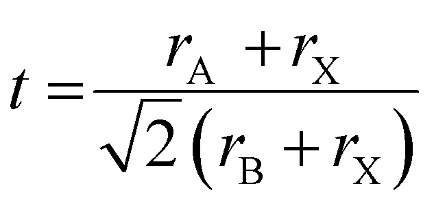 (where rA, rB and rX are ionic radii of the A, B and X-site ions in the ABX3 perovskite structure36) for the CsxFA1−xPbI3 perovskite thin-films, to be used as a rough guide for predicting the perovskite structural phase stability (t ∼ 1) Table S1 (ESI†). Varying the Cs/FA molar ratios yields different t values, which is expected to have a significant impact on the local structure formation and defect-density. Furthermore, to mitigate beam-damage induced artifacts, the total TEM dose was minimized. We used an electron dose rate of ∼1 e Å−2 s−1 for our TEM imaging and diffraction conditions. Based on our results, we found total doses above ∼7 e Å−2 led to a quick degradation of the material (ESI,† Fig. S1 and Videos S1, S2), in agreements with the reported beam-damage doses for FAPbI337 and as a result, our imaging and diffraction conditions were recorded below those values. To study the evolution of crystallographic defects in CsxFA1−xPbI3 perovskite films, we collected low-dose bright field (BF) TEM micrographs and selected-area electron diffraction (SAED) patterns extracted locally from individual domains (Fig. 1). The TEM micrograph of FAPbI3 (Cs0) reveals a prevalence of observable stacking faults (SFs) in striped contrast with widths between 5 to 7 nm in many domains all over the film surface (Fig. 1(a)). An SAED pattern extracted from the domain highlighted with the yellow circle in Fig. 1(a) displays the {111}C twin domains oriented near the [011]C zone axis of the metrically cubic FAPbI3 perovskite Pm
![[3 with combining macron]](https://www.rsc.org/images/entities/char_0033_0304.gif) m crystal structure with a lattice parameter of 6.3 Å (Fig. 1(d)). Note that, throughout the manuscript, the subscripts “c”, “h” and “o” stands for an indexation in the cubic, hexagonal and orthorhombic phases, respectively. Importantly, we observe quantitively a gradual reduction in the {111}C SFs and twin densities with increasing the Cs molar content, (at Cs0.05 & Cs0.1 as shown in ESI,† Fig. S2a, d, b and e) as evident in the BF micrographs and their associated diffraction patterns (DPs). The formation of the {111}C SFs is likely attributed to heterogeneous A-site cation (Cs+ to FA+) distributions, which would allow microscopically unstable regions to form inside the cubic perovskite domains such as the hexagonal photo-inactive δ-FAPbI3 phase. To verify this postulation, helium ion microscopy with secondary ion mass spectrometry (HIM–SIMS) imaging was performed to probe the elemental distribution in CsFA perovskite films. As can be seen in ESI,† Fig. S6a–o, the Cs, Pb, C, N and I elemental mapping shows relatively uniform distribution in the Cs0.15FA0.85PbI3 perovskite absorber (with the exception of Pb–I rich clusters, likely PbI2) compared to the FAPbI3 and Cs0.3FA0.7PbI3 perovskite films which agrees with our hypothesis. Note that, the slightly high signal on the left half of the Cs map in ESI,† Fig. S6h is an artifact, which could be attributed to minor variations in the secondary ion extraction efficiencies during the experiment.
m crystal structure with a lattice parameter of 6.3 Å (Fig. 1(d)). Note that, throughout the manuscript, the subscripts “c”, “h” and “o” stands for an indexation in the cubic, hexagonal and orthorhombic phases, respectively. Importantly, we observe quantitively a gradual reduction in the {111}C SFs and twin densities with increasing the Cs molar content, (at Cs0.05 & Cs0.1 as shown in ESI,† Fig. S2a, d, b and e) as evident in the BF micrographs and their associated diffraction patterns (DPs). The formation of the {111}C SFs is likely attributed to heterogeneous A-site cation (Cs+ to FA+) distributions, which would allow microscopically unstable regions to form inside the cubic perovskite domains such as the hexagonal photo-inactive δ-FAPbI3 phase. To verify this postulation, helium ion microscopy with secondary ion mass spectrometry (HIM–SIMS) imaging was performed to probe the elemental distribution in CsFA perovskite films. As can be seen in ESI,† Fig. S6a–o, the Cs, Pb, C, N and I elemental mapping shows relatively uniform distribution in the Cs0.15FA0.85PbI3 perovskite absorber (with the exception of Pb–I rich clusters, likely PbI2) compared to the FAPbI3 and Cs0.3FA0.7PbI3 perovskite films which agrees with our hypothesis. Note that, the slightly high signal on the left half of the Cs map in ESI,† Fig. S6h is an artifact, which could be attributed to minor variations in the secondary ion extraction efficiencies during the experiment.
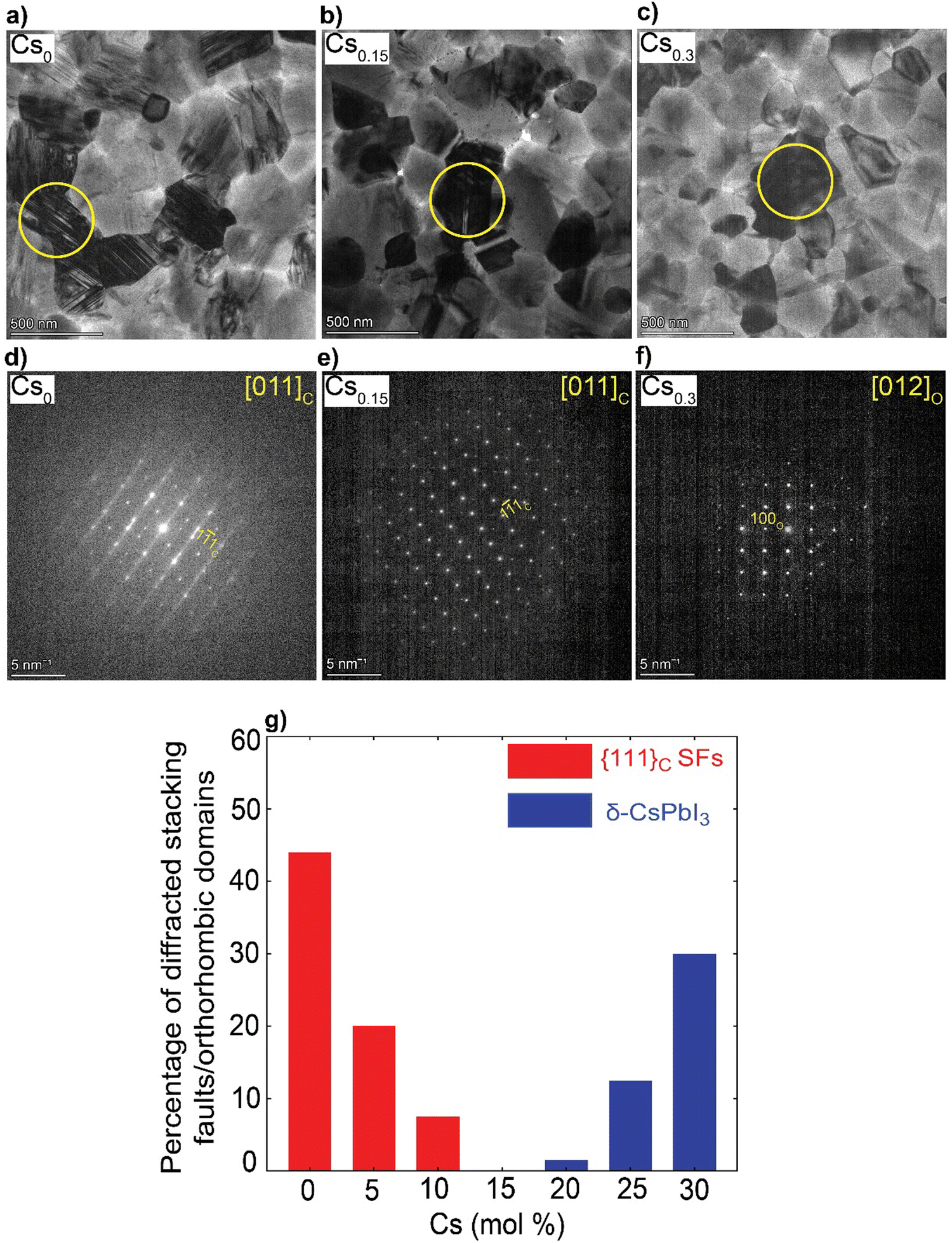 | ||
| Fig. 1 Nanostructural analysis of the CsxFA1−xPbI3 perovskite films: (a)–(c) BF micrographs, (d)–(f) The associated SAED patterns (The Cs content and zone axis are written on the top left and right side of the DPs, respectively), The yellow circles indicate the position of the selected-area for SAED pattern acquisition; and (g) Histograms illustrating the impact of Cs content on the defect density. The estimated percentages are based on the number of diffracted domains (from all the obtained micrographs) featuring {111}C SFs or δ-CsPbI3 phases with respect to all the other different phases present in the samples. | ||
Interestingly, no SFs were detected in Cs0.15FA0.85PbI3 perovskite absorbers in all the metrically cubic structures near the [011]C zone axis (from an analysis of 25 diffraction patterns (DPs) that were obtained across multiple batches and experiments) (Fig. 1(b), (e) and ESI,† Fig. S3a–d). A similar observation was reported by Li et al. for MA0.8FA0.2 when tuning the composition of MAxFA1−xPbI3 perovskite films.37 A further increase in Cs content (x = 0.2–0.3) results in the appearance of unwanted Cs-rich non-perovskite secondary phases known as δ-CsPbI3 as presented in Fig. 1(c), (f) and ESI,† Fig. S2c, f, g and h, Note S1. On the basis of these observations, we conclude that Cs alloying changes the intrinsic FAPbI3 perovskite defect density in which low Cs concentrations (Cs < 15 mol%) reduce the {111}C SFs with a minimum reached at Cs0.15. On the other hand, the presence of CsFA substitutional alloying limit as well as elemental mixing complexities in the precursor stage with high-Cs content (Cs > 15 mol%) tend to trigger the formation of segregated Cs-rich δ-CsPbI3 clusters in the perovskite films.29–31 Therefore, there is a compositional dependence of structural defects prevalence and Cs/FA molar ratios (Fig. 1(g)). We note that we did not observe any single domain that could be indexed with the δ-FAPbI3 crystal structure (2H or even the polytypes 4H and 6H14) in all of the analysed CsxFA1−xPbI3 films, which suggests that single-halide systems have a lower density of bulk hexagonal polytypes compared to mixed-halides.21 For all the Cs-alloyed films, kinematically forbidden reflections in the cubic phase were detected. These can only be indexed to a cubic superstructure with the Im space group near the [011]C zone axis (ESI,† Fig. S4).38 Recently, Doherty et al. studied these forbidden reflections in similar FA-rich perovskite compositions such as CsMAFA, attributing them to octahedral tilting whereby the BX6 corner-sharing octahedra slightly tilt away from a perfect cubic symmetry in a long-range ordered fashion.22 The unit cell parameter of the Im space group is effectively doubled (∼12.6 Å) with the structural ordering of the lattice tilting, leading to so-called superlattice reflections. However, since we did not observe any of these superstructure reflections in the neat FAPbI3 films from a study of hundreds of DPs, we cannot exclude the possibility of CsFA cation ordering on the A-site as a driving force for these superlattice reflections in these alloyed systems. Moreover, upon in situ annealing of a pure FAPbI3 film inside the TEM at 170 °C, we detected the emergence of hexagonal polytype phases with a domain that could be indexed to the 6H-FAPbI3 phase along the [37![[2 with combining macron]](https://www.rsc.org/images/entities/char_0032_0304.gif) ]H zone axis as highlighted in ESI,† Fig. S5. This observation indicates the thermal decomposition of the metrically cubic FAPbI3 film is possibly due to FA+ loss which results in a change of the corner-sharing stacking sequence (metrically cubic perovskite) to a mix of corner-face sharing octahedra (hexagonal polytypes) when annealed at elevated temperatures. Prolonged heating under vacuum should eventually lead to lattice shrinkage, morphology deformation and degradation of the perovskite film.39
]H zone axis as highlighted in ESI,† Fig. S5. This observation indicates the thermal decomposition of the metrically cubic FAPbI3 film is possibly due to FA+ loss which results in a change of the corner-sharing stacking sequence (metrically cubic perovskite) to a mix of corner-face sharing octahedra (hexagonal polytypes) when annealed at elevated temperatures. Prolonged heating under vacuum should eventually lead to lattice shrinkage, morphology deformation and degradation of the perovskite film.39
The perovskite films were examined macroscopically using X-ray diffraction (XRD) measurements, shown in Fig. 2(a). The 001, 011, 111, 002, 012, 022 and 003 of the metrically α-cubic FAPbI3 perovskite structure in addition to peaks corresponding to PbI2 and the ITO substrate are present. Although, the inks containing 10 mol% excess PbI2 for all compositions, which is reported to improve efficiency,40 we noticed a change in the relative 001 PbI2 to 001 perovskite peak intensities located at 12.67° and ∼14°, respectively. We rationalize this observation by the likelihood of the existence of definite packaging density of Cs-ions relative to FA+ on the A-site of the perovskite lattice to form the metrically cubic phase where the threshold is found to be at Cs0.15. Upon exceeding this limit (Cs > 15 mol%) and with the oversupply of Cs-ions, the perovskite lattice starts to be likely strained and gradually decomposes into PbI2.41 The Cs0.15FA0.85PbI3 perovskite film exhibits the smallest full-width at half maximum (FWHM) for the main 001 perovskite peak in addition to the highest relative intensity of 001 perovskite to 001 PbI2 peaks, inferring enhanced crystalline ordering of the perovskite lattice (Fig. 2(b)). Furthermore, the incorporation of the smaller-sized Cs cation into the FAPbI3 crystal lattice leads to a shift to higher angles for the 002 perovskite peak, implying smaller d-spacings and hence, lattice contraction (Fig. 2(c)). For the Cs0.3FA0.7 films, we observe a peak broadening and a disruption of the aforementioned trend where the peaks do not stagnate with respect to width and position, but are broader and weaklier defined, indicating unsuccessful Cs-incorporation and actual disruption of the crystal lattice symmetry at these higher concentrations. Additionally, HIM–SIMS measurements (ESI,† Fig. S6k–o) demonstrate the distinct formation of segregated CsPbI3-rich clusters. These observations are consistent with the previous reports about the presence of a Cs-substitution limit in CsFA alloying.30
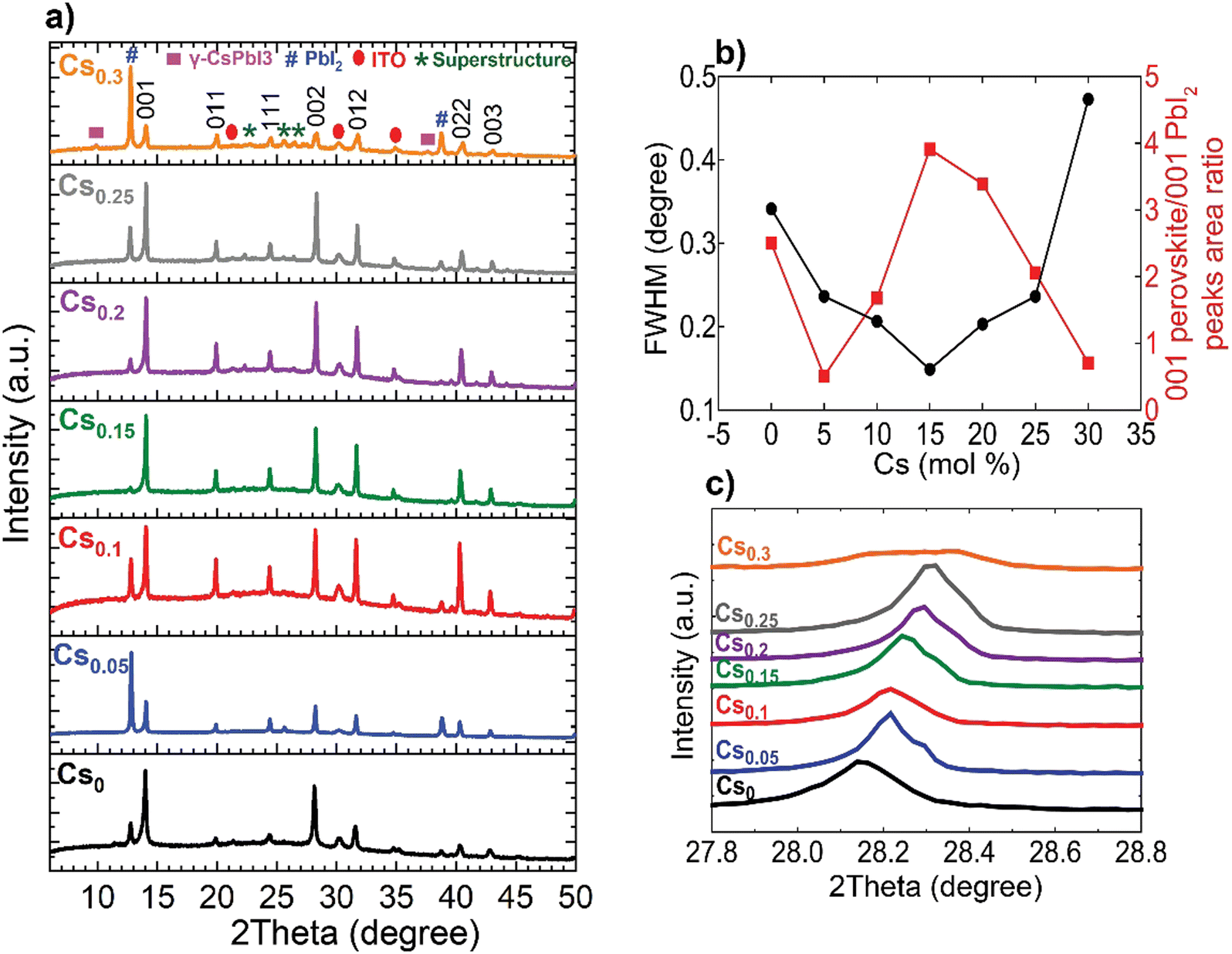 | ||
| Fig. 2 Macroscopic structural analysis of the CsxFA1−xPbI3 perovskite films: (a) XRD patterns, (b) Analysis of the FWHM of the 001 perovskite peak and relative 001 perovskite/001 PbI2 as a function of the Cs content and (c) zoomed-in view of the 002 perovskite peak highlighting shift to higher angles with increasing Cs content indicative of a lattice contraction. | ||
Morphologically, the perovskite surface of the FAPbI3 film consists of rough (verified by atomic-force microscopy (AFM) in ESI,† Fig. S8) terraced-edges, which are likely SFs based on our TEM data, as corroborated by scanning electron microscopy (SEM) images in ESI,† Fig. S7a. In stark contrast, the CsFA alloyed films display well-defined domains and a decrease in domain sizes relative to FAPbI3 films with increasing Cs content (ESI,† Fig. S7b–g). Here, we refer our discussion to an overlooked aspect in perovskite literature: domain crystal quality rather than domain size. It is widely accepted that growing large grains with fewer grain boundaries is beneficial for charge transport and thereby, gaining efficiency improvements.42–44 However, it was recently reported that SEM observations are usually based on morphological domains comprised of multiple grain entities rather than being singular grains themselves and that the domains’ local orientations are much more critical than their sizes.45 In concert with these observations, we found that Cs0.15FA0.85PbI3 films possess relatively smaller-domain sizes but are SF-minimal indicating higher structural quality. Meanwhile, low Cs-content (Cs0.05FA0.95PbI3 and Cs0.1FA0.9PbI3, respectively) alloyed films consist of larger domains with considerably higher densities of SFs. Therefore, this calls for diverting efforts into the promotion of the domain quality through the elimination of structural disorders rather than seeking to only enhance the domain size. Needless to say, an ideal growth condition entails creating large domains with high crystal quality perovskite films.
To investigate how these structural and morphological features influence the films’ optoelectronic properties, we first sought to address whether those nanoscale defects contribute electronically to shallow or deep trap states. To test for the presence of shallow traps, we performed ultra-sensitive external quantum efficiency (EQE), kelvin-probe force microscopy (KPFM) measurements (Fig. 3). Ultra-sensitive EQE measurements were conducted on encapsulated CsxFA1−xPbI3 perovskite devices using a home-built sensitive EQE apparatus.46Fig. 3(a) shows the normalized EQE spectra of CsxFA1−xPbI3 devices plotted as a function of photon energy, and compared for different concentrations of Cs. We note that the sharp peak located at approximately 0.92 eV is electrical device- and/or EQE apparatus-related pick-up noise since the genuine spectral features in the EQE are never as sharp as this 0.92 eV peak.47 On the other hand, the line-shape of all perovskite EQE spectra is dominated by the 0.85 eV and 1.2 eV interference peaks, which includes an additional, Cs-concentration dependent, mid-gap trap signal (see inset in Fig. 3(a)), this is expected and in line with the literature.48 As shown from the integrated sub-gap EQE (inset in Fig. 3(a)), where the integrated area can be treated as rough measure for relative changes in trap signal/density (under the condition that the device thickness is the same, hence, interference effects are the same), with a reduction upon Cs-alloying, likely linked to improved performance through reduced recombination losses.49,50 The apparent Urbach energy spectra,51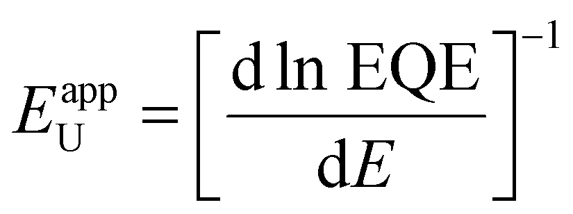 , were calculated based on the normalized EQE spectra, and are shown in Fig. 3(b). Here, the Urbach energy is found to be approximately 11.5 ± 1 meV for all perovskite devices (inset in Fig. 3(b)) indicative of the absence of Cs-induced changes in shallow trap (or tail) states.47 We further tracked the impact of Cs alloying on the surface potential distributions using KPFM. It is worth noting that surface defects can modify the potential distributions of perovskite surfaces.52 Since these measurements were done under ambient conditions and subsequently, consecutive measurements on the same scan area may not always yield the same absolute values, we focused our interpretation only on surface potential variations (degree of homogeneity) and not absolute potential values. As shown in Fig. 3(c)–(e) and ESI,† Fig. S9a–d, the surface potential fluctuations of all perovskite films were comparable regardless of Cs content. The standard deviations of surface potential distributions are presented in Fig. 3(f) and the electronic-roughness values are compared in ESI,† Fig. S9e. To verify our surface potential findings and exclude the possibility of any topographical features induced artifacts (such as valleys present at grain boundaries that might not be detected by the tip), we plotted correlation maps between the surface topography and potential values as shown in ESI,† Fig. S10a–g. We then were able to firmly conclude that they are not correlated with very low correlation factors (R) < 20%, confirming the soundness of our experimental results (ESI,† Fig. S10h). Likewise, there is no signature of differences in surface potential mimicking the shape of the observed striped contrasts due to stacking faults. This means that the observed potential variations do not reflect directly in a change in surface potential.
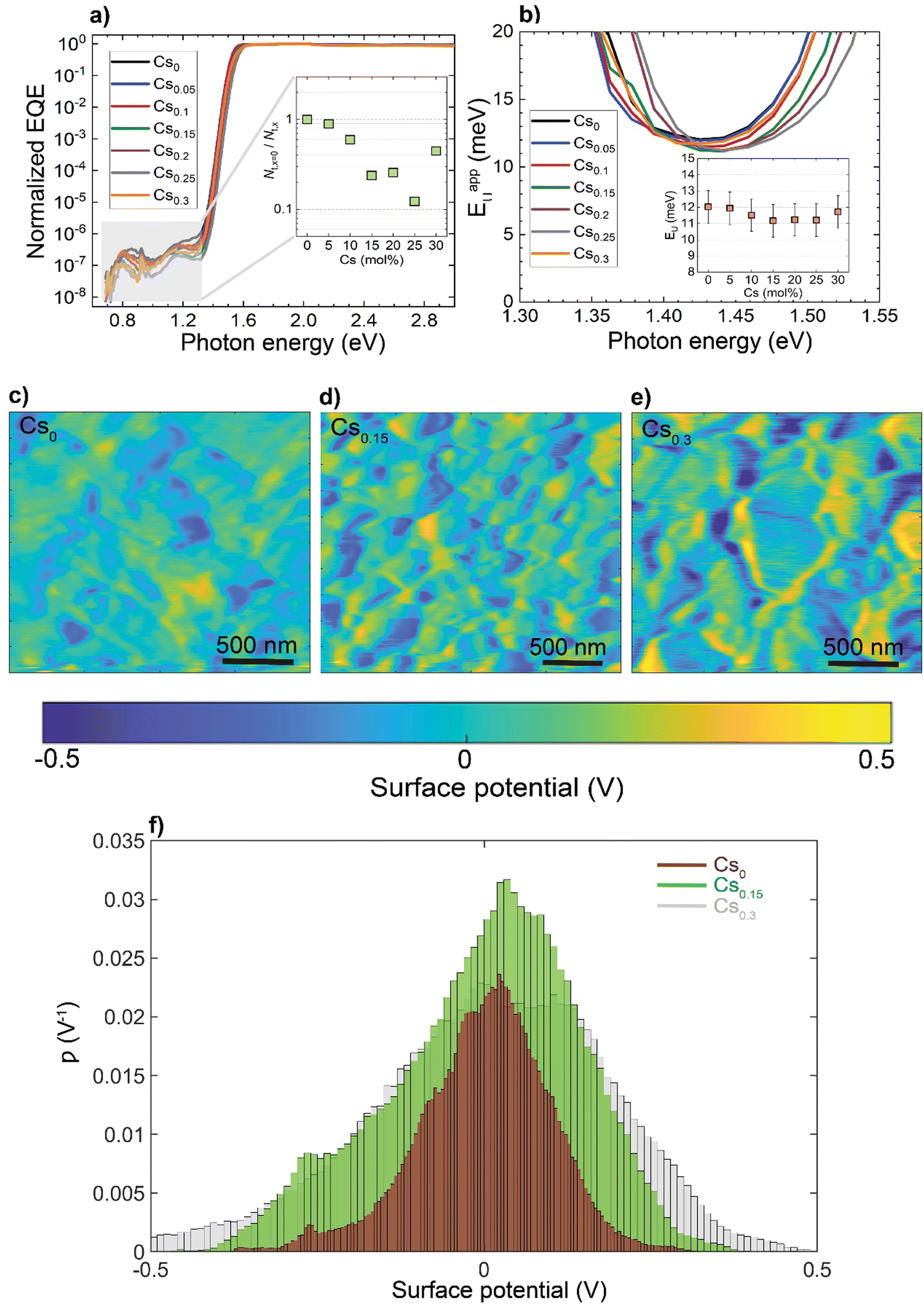 | ||
| Fig. 3 The impact of Cs alloying on electronic trap states: (a) normalized EQE of CsxFA1−xPbI3 perovskite devices plotted as a function of photon energy. The inset shows the change of deep trap signal with Cs content as obtained from the integral of EQE in the trap-limited area versus Cs fraction in CsxFA1−xPbI3 perovskite devices, (b) apparent Urbach energy spectra of the devices plotted as a function of photon energy. The inset shows the Urbach energy spectrum against the Cs concentration with error bars corresponding to the ±1 meV uncertainty in Urbach energy determination, (c)–(e) Surface potential maps for the CsFA perovskite films and (f) corresponding distribution (ρ) plots of the relative surface potential shifts for the perovskite films. | ||
Furthermore, measurements of photoluminescence quantum yield (PLQY) versus Cs concentration show only a minor effect of Cs content on the film-averaged non-radiative recombination rate at 1-sun illumination intensity (ESI,† Fig. S11). Taken together, these measurements suggest that these structural defects are not inducing either surface or deep traps and hence, are not sites of significant recombination losses.
Applying temperature-dependent ultra-sensitive EQE measurements on unencapsulated CsxFA1−xPbI3 PSCs, we were able to probe the dynamic (Edyn) and static (Estat) energetic disorder.53 The latter has been shown to be intrinsically related to zero point motion of phonons rather than structural imperfections,47,54 while the former is a metric for temperature-dependent phonon occupation (proportional to phonon energy).55 We note that the temperature regime (between 25 °C to −120 °C) was chosen such that phase-transition of the main perovskite structure (i.e., FAPbI3) at the higher and lower temperature limits were avoided.52 ESI,† Fig. S12a–g displays the normalized EQE of the CsxFA1−xPbI3 perovskite devices (x = 0, 0.5, 0.1, 0.15, 0.2, 0.25, and 0.3, respectively) plotted as a function of photon energy and compared against different temperatures. The insets show the corresponding calculated apparent Urbach energy spectra, from which the Urbach energies were determined. The Urbach energy for the CsxFA1−xPbI3 perovskite devices at room temperature were found to be 12.1 ± 1 meV (x = 0), 11.5 ± 1 meV (x = 0.05), 11.8 ± 1 meV (x = 0.1), 11.0 ± 1 meV (x = 0.15), 11.5 ± 1 meV (x = 0.2), 11.9 ± 1 meV (x = 0.25), and 11.5 ± 1 meV (x = 0.3). These values are in good agreement with Urbach energy values obtained on encapsulated devices in inset Fig. 3(b). ESI,† Fig. S13a–g shows Urbach energy values plotted against the temperatures and compared for all the CsxFA1−xPbI3 PSCs. While symbols are experimental data, black solid lines are fits to the Einstein solid model: 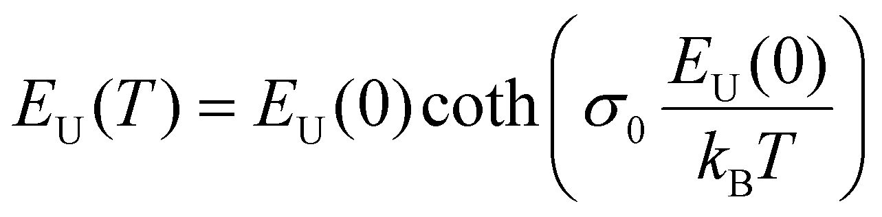 , where
 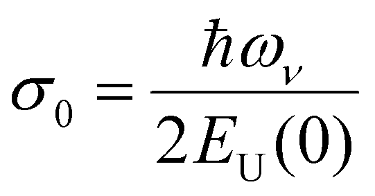 is a temperature-independent constant, ωv is a characteristic phonon frequency, ℏ is the reduced Planck constant, and kB is the Boltzmann constant.47 Based on the Einstein solid model, temperature-induced Edyn and E0 disorder contribute to Urbach energy EU(T), via EU(T) = [E0 + Edyn]/σ0, where E0 is expected to dominate at the low-temperature limit (i.e., for T → 0, EU(T) →E0). E0 (defined here as phonon zero-point energy) is found to be 3.26 ± 0.24 meV (x = 0), 3.82 ± 0.09 meV (x = 0.05), 3.75 ± 0.15 meV (x = 0.1), 4.55 ± 0.18 meV (x = 0.15), 5.39 ± 0.09 meV (x = 0.2), 6.68 ± 0.13 meV (x = 0.25), and 4.00 ± 0.15 meV (x = 0.3). The Urbach energy at room temperature, EU(RT), the Einstein solid mode fit parameter E0 and σ0, and the calculated approximate Einstein temperature,
 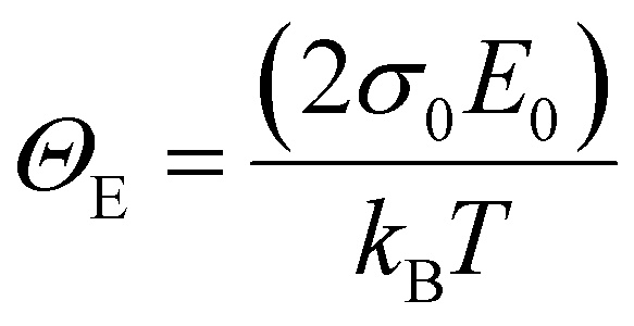 , and phonon wavenumber are provided in Table S2. The corresponding calculated wavenumbers match very well to Pb–I octahedral and cage-cation phonon modes, respectively, as obtained from Raman spectroscopy, reported in the literature.53–55 While the Einstein solid model can be extended by introducing an additional term Estruc to account for, inter alia, defect state-induced structural disorder, however, only for Estruc = 0 reliable fits of EU(T) for the CsxFA1−xPbI3 perovskite devices were achieved. The absence of an additional structural disorder in these materials suggests that static disorder is solely dominated by quantum mechanical phonon lattice vibrations (phonon zero-point energy).49 This indicates that the introduction of Cs atoms in the perovskite lattice does not impose structural deformations as our data can be explained by a simple Einstein solid model with no need for an additional structural disorder as expected for example with amorphous silicon (a-Si),47 which is in accordance with our observation of almost no changes in Urbach energy with Cs doping.
Next, to investigate the effects of the nanoscale defects on the photo-conductivity of the CsFA perovskite films, we performed time-resolved microwave conductivity (TRMC) measurements and observed a comparable increase of carriers’ mobilities in the range of 30–40 cm2 (V s)−1 upon Cs introduction, except for the Cs0 as shown in Fig. 4(a). Notably, these values present intra-grain/domain “within the internal structure of the grain itself” mobilities, yet barriers at the edges of domains may result in effective reduced mobilities throughout the film.56 We further note that the TRMC traces are recorded at an incident light intensity of 5.5 × 10⁹ photons per cm2 per pulse, which corresponds to an initial charge carrier density of approximately 1014 cm3 per pulse. Complementarily, we conducted impedance spectroscopy and potentiostatic polarization measurements (see ESI,† Note S2 for details),57,58 and observed that the electronic conductivity (σelectronic) is maximized in the Cs0.15FA0.85PbI3 perovskite film, while the ionic conductivities (σionic) decrease with increasing Cs content (ESI,† Fig. S14a and b). We suspect that this change in ionic conductivity is related to a change in lattice constant upon Cs incorporation (Fig. 2(c)). It has been shown that compression of the lattice reduces ion migration by increasing the associated activation energy.59 In addition, we find that the ion densities (nion) remain almost constant with increasing Cs content (ESI,† Fig. S14c). As a result, the change in ionic conductivity is probably related to a change in the ion mobility.
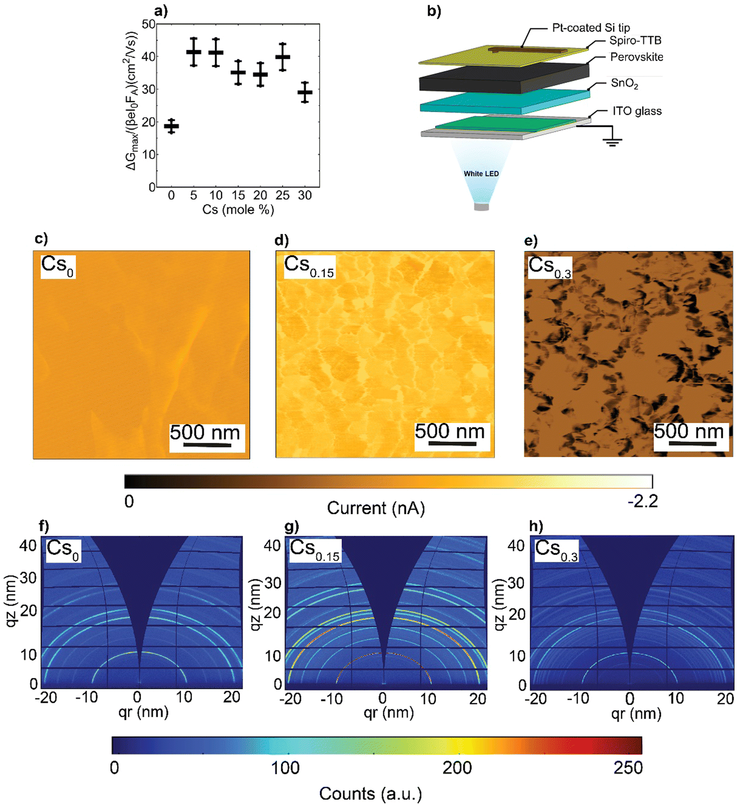 | ||
| Fig. 4 Optoelectronic properties and crystal orientation: (a) charge carrier mobility values calculated from TRMC measurements with error bars corresponding to 10% uncertainty, (b) Experimental setup of the C-AFM measurements where a conductive tip is functioning in contact mode, (c)–(e) Photo-current maps performed at 1 sun under JSC conditions for the CsFA perovskite systems and (f)–(h) 2D GIWAXS patterns of the CsFA perovskite films. | ||
To evaluate the local photo-current at a nanoscale, conductive-atomic force microscopy (C-AFM) was used with a white LED providing ∼1 sun excitation, as shown in Fig. 4(b). The energy-levels diagram for the different layers comprising the pseudo-device stack and the work function (WF) of the platinum (Pt)-coated silicon (Si) tip are depicted in ESI,† Fig. S15, based on prototypical literature values.60–62 Note, to enable local information, we refrained from depositing metal electrodes, which would collect charge-carriers from a larger area due to their high lateral conductivity, i.e., reducing spatial resolution. As can be seen in Fig. 4(c)–(e), the spatial photo-current conductivity and homogeneity are peaked in Cs0.15FA0.85PbI3 perovskite system compared to the Cs0 and Cs0.3 pseudo-devices, indicative of effective carriers’ transport and collection properties. This trend agrees with the short-circuit current (JSC) obtained from full devices (presented later in Fig. 5(c)) with an R = 0.63 in ESI,† Fig. S16. These results provide an indication that nanoscale defects rather than charge carriers’ mobilities retard the charge carrier transport within the CsFA absorber layers. Therefore, we can conclude that the increased conductivity in Cs0.15FA0.85PbI3 is more likely attributed to the high crystal perovskite film quality. Moreover, although the SFs/Cs-rich clusters do not reduce the intra-grain carrier mobility, they seem to affect the inter-grain (across a set of individual grains) transport, as evidenced by C-AFM measurements.
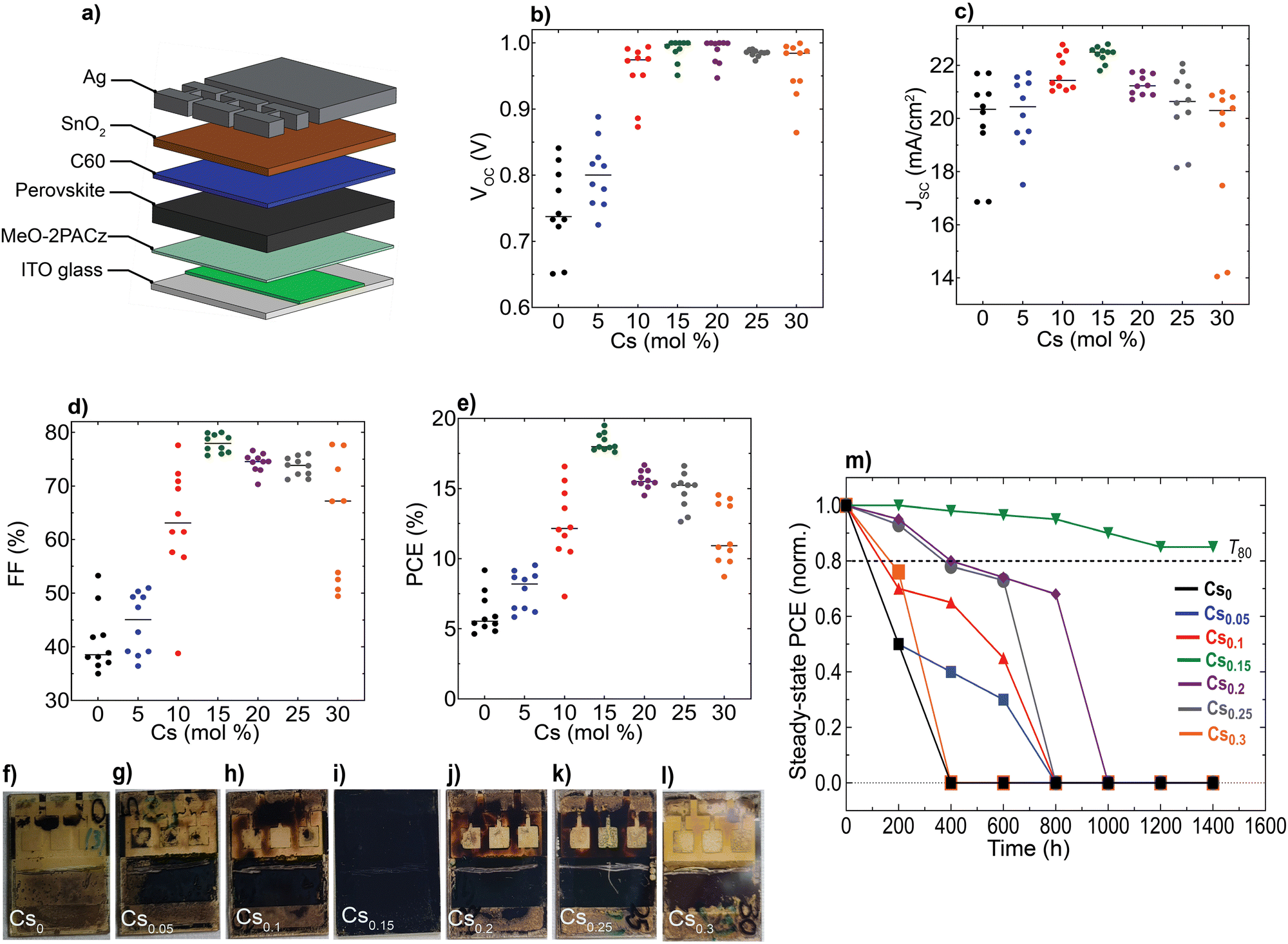 | ||
| Fig. 5 Device performance and operational stability of the perovskite devices: (a) schematic illustration of the pin device stack, Statistical distribution for the device performance metrics of the CsFA PSCs: (b) VOC, (c) JSC, (d) FF, (e) PCE. All JV data were acquired at standard conditions under a simulated air mass (AM) 1.5G and 100 mW cm−2 of sunlight, (f)–(l) Photographs of the aged CsFA encapsulated perovskite devices taken from the glass side after 1400 hours of continuous simulated sunlight illumination and (m) Evolution of normalized (norm.) steady-state PCE (averaged from 6 sub cells) for encapsulated PSCs, aged under continuous simulated sunlight illumination at 35 °C in N2 atmosphere, T80 defines the time required for a solar cell device to drop to 80% of its initial efficiency. | ||
Since the photo-electric properties such as JSC of metal–halide perovskites vary greatly among different facets,63–65 we used 2D synchrotron grazing-incidence wide-angle X-ray scattering (GIWAXS) to probe the in- and out-of plane films’ texture. As shown in Fig. 4(f)–(h) and ESI,† Fig. S17a–d, theCsxFA1−xPbI3 (x = 0.05, 0.1, 0.15, 0.2 and 0.25, respectively) perovskite films display similar diffraction rings in the 001 and 002 main perovskite peaks at q about 10 and 20 nm−1, respectively. Notably, upon Cs alloying (pronounced even at Cs0.05), the random azimuthal orientation observed in the FAPbI3 film shifts to a mild preferential 001 face-up orientation66 relative to the substrate coinciding with a corner-up orientation of the 011 perovskite plane (ESI,† Fig. S18a–d). This plausibly further supports that the SFs/Cs-rich defective phases impose transport losses rather than the crystal orientation.
We aimed to investigate the impact of the differences observed in nanostructure and optoelectronic properties on the device performance and long-term operational stability for different Cs content inCsxFA1−xPbI3 PSCs, while keeping the hole/electron transport layers and device configuration the same. We fabricated devices using an inverted (p–i–n) architecture based on indium-tin oxide (ITO) glass/(2-(3,6-dimethoxy-9H-carbazol-9-yl)ethyl)phosphonic acid (MeO-2PACz)/perovskite/buckminsterfullerene (C60)/tin(IV)oxide (SnO2)/silver (Ag), as sketched in Fig. 5(a). Remarkably, the Cs0.15FA0.85PbI3 perovskite film reached a maximum PCE of 19.3% with a JSC of 22.8 mA cm−2, an open-circuit voltage (VOC) of 1.02 V and a fill-factor (FF) of 82.8% (Fig. 5(b)–(e)). We further attempted to link the device data to the films’ optoelectronics. First, we performed a performance loss-breakdown analysis by extracting the quasi-Fermi level splitting (QFLS) for different charge-transport layers (CTLs)/perovskite combinations in comparison to the mean qVOC of the devices. The losses are comparable for all stacks, however, we noticed major differences between the obtained qVOC and QFLS for the poor-performing (notably Cs0 and Cs0.05) devices, as shown in ESI,† Fig. S19. We sought to understand this effect with a link to carriers’ mobility and therefore, conducted a set of drift-diffusion simulations rendering qualitatively a similar effect with respect to the VOCversus QFLS (albeit significantly less severe) and likewise a drop in the other PV metrics below a mobility of 1 cm2 V−1 s−1, as shown in ESI,† Fig. S20. The qualitative similarity between the QFLS/VOC trend is in perfect agreement with a recent study by Warby et al.,67 yet there is a significant quantitative disagreement. We tried to understand this disagreement in greater detail and re-examined the current–voltage (JV) statistics and found that the missing link is the systematically lower apparent shunt resistance in the cells with Cs-content <15% contributing to a lower VOC, FF and JSC in addition to the other detrimental effects due to the unfavourable nanostructure properties (ESI,† Fig. S21). Thus, we point out that the poorer intrinsic nano-structural quality of the perovskites with various Cs content (except Cs0.15FA0.85PbI3) together with a lower apparent shunt resistance account for the observed effects on device performances. Notably, we extracted the apparent shunt resistance as a function of illumination intensity and observed a strong intensity-dependence, in particular for the lowest-performing Cs0 samples (ESI,† Fig. S22). A classical electrical shunt (i.e., direct connection of the ITO to Ag) would not have such an intensity-dependence. In contrast, impaired charge collection, e.g., through a reduced mobility of at least one of the charge carriers, results in such a behaviour, more commonly observed in, e.g., organic or similarly excitonic solar cells. These observations are in full accord with results by Elmestekawy et al.,68,69 who show a comparable reduction of intrinsic quantum confinement in FAPbI3 upon Cs substitution and discuss the impact of reduced confinement on device performance. Our investigations complement these observations via a nanoscopic investigation where the origin of said confinement is likely the nanoscopically separated domains emerging from the shown SFs and in excellent agreement with the predictions by Wright et al.70 Voltage-dependent EQE measurements suggest that primarily the hole transport is limited in the case of low Cs substitution (ESI,† Fig. S23).
Furthermore, we aged unencapsulated perovskite absorbers at constant simulated solar spectrum illumination in ambient atmosphere without an ultraviolet (UV) filter at ∼65 °C (ESI,† Fig. S24). In parallel, encapsulated devices (with cover slip and UV-cured glue) were aged under continuous full-spectrum of 1 sun illumination at 35 °C and open-circuit conditions in a nitrogen (N2) environment (Fig. 5(m) and ESI,† Fig. S25). We note that ageing PSCs at open-circuit conditions is reported to accelerate degradation compared to maximum power point tracking (MPP).71 Notably, the optimum Cs0.15FA0.85PbI3 perovskite device sustained 85% of its initial PCE for 1400 hours, whereas all the other devices completely degraded within comparatively different and shorter timescales, consistent with their yellowish-visual appearances (Fig. 5(f)–(l)), particularly in the device-active area regions which is indicative of PbI2 phase formation generated as a by-product of the absorber layers decomposition.72
Finally, we conducted accelerated ageing combining electrical and thermal stress testing under 1 sun illumination at a higher temperature of 85 °C in ambient atmosphere for unencapsulated devices at MPP conditions, following the standardized international summit on organic PV stability (ISOS) protocols73 (Fig. 6(a)). This accelerated ageing study uses the same device configuration shown in Fig. 5(a). The Cs0.15FA0.85PbI3 perovskite device maintained 95% of its peak performance for 40 hours. In contrast, the Cs0 and Cs0.3 PSCs degraded faster over the same measurement period with a similar ‘burn-in’ degradation period after 40 hours. To investigate the long-term intrinsic structural stability, we further performed XRD measurements for aged CsFA perovskite films that were stored in a N2 environment under full-spectrum sunlight illumination for a duration of 2, 280 hours (Fig. 6(b)). The structural analysis of the aged films reveals the emergence of the photo-inactive δ-2H FAPbI3 and γ-CsPbI3 phases manifested by Bragg peaks at 2Theta angles of 11.78° and 13.29°, respectively. The δ-2H FAPbI3 phase appears for the Cs0, Cs0.05 and Cs0.1 perovskite films, while the δ-CsPbI3 phase shows in Cs0.2 and Cs0.25 films. We point out that these phases were not detected in our fresh films (Fig. 2(a)). Significantly, the Cs0.15FA0.85PbI3 perovskite absorber retained the metrically cubic perovskite peaks with no detection of unwanted secondary phases, confirming the robust structural stability. These results validate our argument based on the TEM observations, that the presence of subtle structural imperfections such as hexagonal/orthorhombic phases, undetected with bulk XRD measurements, stimulate the growth of degradation sites under operational stressors, which deteriorate the device longevity. The behaviour of the relative intensities of the 001 perovskite to PbI2 peaks is similar for fresh and aged samples, as compared in Fig. 6(c), which demonstrates enhanced perovskite crystallinity for the Cs0.15FA0.85PbI3 perovskite absorber. We thus conclude that PbI2 particles, SFs and Cs-rich clusters are the most problematic phase impurities and are key drivers for absorber layer degradation on the long-term. Overall, our collective findings endow that despite the defect tolerance of perovskite materials with respect to the initial optoelectronic properties and device performance, these nanoscale defective phases seed degradation on the longer run which ultimately limit the device operational stability.
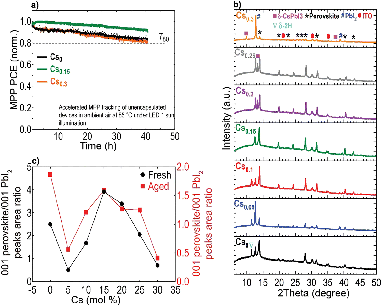 | ||
| Fig. 6 Accelerated aging tests and long-term structural stability: (a) MPP stability tracking (norm.) of unencapsulated perovskite devices under simulated sunlight at 85 °C in ambient conditions at a relative humidity level <20%, (b) XRD patterns of CsFA perovskite films, aged for 2280 hours under continuous simulated sunlight illumination at 35 °C in N2 atmosphere (the marked ‘*’ perovskite peaks include both the metrically cubic and superstructure phases) and (c) Relative intensities of 001 perovskite/001 PbI2 peaks for fresh and aged perovskite films. | ||
Conclusion and outlook
Our work provides fundamental guidelines for engineering state of the art FA-rich perovskite absorbers pairing enhanced intrinsic stability with efficient device operation through the elimination of stacking faults in the desired α-FAPbI3 cubic phase at room temperature. We have studied the nanostructure-properties relationships in theCsxFA1−xPbI3 perovskites and assessed their impact on macroscopic devices with respect to performance and stability under operational conditions. We showed the effect of CsFA cation alloying on controlling the nanoscopic defects landscape and emphasized the vital role of attaining a minimal stacking fault perovskite absorber in enhancing the electronic conductivity, device performance and operational stability. Importantly, we urge for the significance of careful A-site compositional tuning in FA-rich perovskite absorbers that target high domain crystal quality. Our results represent a clear demonstration of linking the nanoscopic landscape to the device long-term operational stability, which attests to the importance of this fundamental investigation. Future research entailing the fundamental understanding of performance-limiting nanoscale phases in halide perovskites will emerge as a new domain for pushing the stability aspects in perovskite devices.Methods
Materials
Lead-iodide (PbI2) beads (purity ≥99.999%) were purchased from Alfa Aesar. Anhydrous DMF (dimethylformamide), anhydrous DMSO (dimethyl sulfoxide), ethanol and ethyl-acetate (EA) were purchased from Sigma Aldrich. Formamidinium iodide (FAI) was purchased from Dyenamo. Cesium iodide (CsI) and MeO-2PACz were purchased from TCI. All chemicals were directly used as received.Perovskite thin film preparation
The perovskite composition used isCsxFA1−xPbI3. 1 M solutions of both neat FAPbI3 and CsPbI3 films were prepared in mixed solvents of DMF/DMSO (volume ratio 4![[thin space (1/6-em)]](https://www.rsc.org/images/entities/char_2009.gif) :1) and then mixed by volume to get the desired nominal molar concentrations. Both precursor solutions contain a 10 mol% excess PbI2. A perovskite film with ∼350 nm thickness was then deposited on cleaned ITO glasses by spin coating 100 μl of the 1 M precursor solution (for PSC fabrication in a two-step spinning program: 1st at 1000 revolutions per minute (rpm), 200 rpm s−1 for 10 s and 2nd at 5000 rpm, 800 rpm s−1 for 35 s) or 0.6 M precursor solution to obtain a film thickness of ∼150 nm (for TEM specimen preparation in a one-step spinning program: 11000 rpm, 11000 rpm s−1 for 35 s). For the antisolvent quenching, 5 s before the end of the spin coating, 300 μl of EA was quickly dropped onto the perovskite surface. The deposited films were then immediately annealed at 150 °C for 30 min. All the film and device fabrication processes were done inside a glovebox filled with N2 atmosphere.
:1) and then mixed by volume to get the desired nominal molar concentrations. Both precursor solutions contain a 10 mol% excess PbI2. A perovskite film with ∼350 nm thickness was then deposited on cleaned ITO glasses by spin coating 100 μl of the 1 M precursor solution (for PSC fabrication in a two-step spinning program: 1st at 1000 revolutions per minute (rpm), 200 rpm s−1 for 10 s and 2nd at 5000 rpm, 800 rpm s−1 for 35 s) or 0.6 M precursor solution to obtain a film thickness of ∼150 nm (for TEM specimen preparation in a one-step spinning program: 11000 rpm, 11000 rpm s−1 for 35 s). For the antisolvent quenching, 5 s before the end of the spin coating, 300 μl of EA was quickly dropped onto the perovskite surface. The deposited films were then immediately annealed at 150 °C for 30 min. All the film and device fabrication processes were done inside a glovebox filled with N2 atmosphere.
For TEM experiments: the perovskite films were directly spin-coated on ultra-thin C-coated Cu TEM grids that were sticked to ITO glass using a Kapton tape. To minimize any environmental potential-induced degradations such as moisture exposure, the samples were placed in a nitrogen (N2)-filled cylinder immediately after deposition inside the glovebox and then transferred into the TEM chamber in less than 5 mins of air exposure.
PSCs fabrication
ITO glass substrates were washed with deionized water for 15min followed by 10 min water-bath sonication. The cleaned substrates were treated by ultraviolet (UV) ozone for 10 min. After UV ozone treatment, 1mgml−1 of MeO-2PACz self-assembled monolayer (SAM) solution (hole-transport layer) dissolved in ethanol was spin-coated on substrates at 3000rpm for 30s in a N2-filled glovebox, followed by annealing at 100°C for 10min. The spin-coated CsFA perovskite films were deposited on top of MeO-2PACs and then annealed at 150 °C for 30 min. An electron-selective stack of C60 (20nm, >99.95%, NanoC) was then thermally evaporated in a home-made evaporation system (base pressure <2 × 10⁻⁶ mbar, working pressure >3 × 10⁻⁶ mbar, evaporation rate of 0.3 Å s−1 as measured by quartz crystal monitors, aluminium oxide crucibles with power applied to the sources of ∼50 watt, the substrate holder was maintained at room temperature). A buffer layer of 25nm of SnO2 was deposited by atomic layer deposition using an Oxford Instruments system at 100 °C using tetrakis(dimethylamino) tin and H2O as precursors. To finish the full-device, 130 nm of silver (Ag) was thermally evaporated through a shadow mask on the samples. During all the thermal evaporations, the deposition rate was first stabilized to the targeted value before opening the substrate shutter. We note here that the TEM specimens were exposed to only 4 mins of UV-ozone treatment.
TEM characterization
BF micrographs and SAED patterns were acquired on a Talos F200S TEM operating at 200 kV and located in the Centre interdisciplinaire de Microscopie électronique (Cime) of EPFL, Lausanne campus. To minimize any possible electron beam-induced artifacts, we used low-dose TEM imaging conditions, with an electron dose rate of ∼1 e Å−2 s−1. All the TEM BF micrographs and diffraction patterns were recorded from previously unexposed regions of the sample. Furthermore, the specimen was never tilted and the SAED patterns were taken at whatever orientation the domains were found in. A small objective aperture of 10 μm size was used to enable the record of localised DPs. The SAED patterns were analysed using JEMs software.(Temperature dependent) ultra-sensitive EQE
A UV/VIS/NIR spectrophotometer (PerkinElmer, Lambda 950) was used as a source of monochromatic light. The probe light was physically chopped at 273 Hz and directed with different optical components onto the device under test (DUT). Prior recording the DUT response with a lock-in amplifier (Stanford Research, SR860), the DUT photocurrent was amplified by a current pre-amplifier (FEMTO, DLPCA-200). The DUT was mounted in an electrically shielded sample holder (Linkam, LTS420E-P); for temperature dependent measurements, the sample holder was connected to a liquid nitrogen pump (Linkam, LNP96) and a temperature controller (Linkam, T96). For calibration, a NIST-calibrated Si (Newport, 818-UV) and Ge (818-IR) photodiode sensor were used as reference devices. Detailed information about the EQE apparatus is provided elsewhere.46Potentiostatic polarization measurements
Gold contacts with a thickness of 100 nm were thermally evaporated (Nexdep, Angstrom Engineering) onto the perovskite films through a shadow mask with a diameter of 1 mm to measure the electronic and ionic conductivity. The complex impedance was measured from 0.1 Hz to 1 MHz with an amplitude of 50 mV using a Paios measurement system (Fluxim AG). The complex electric modulus was fitted to extract the effective ionic conductivities. DC polarisation curves were also acquired with the Paios instrument by applying a constant potential of 0.2 V and measuring the current over 10 minutes. The electronic conductivity was calculated from the steady-state current value.XRD
Carried out in an Empyrean diffractometer (Panalytical) equipped with a PIXcel-1D detector, located at EPFL, Lausanne campus. The XRD patterns were obtained using the Cu Kα radiation (wavelength of 1.54 Å).SEM
SEM images were acquired with an acceleration voltage of 3 kV and probe current of 110 pA using an in-lens detector in a Zeiss GeminiSEM 450 microscope. The dwell time for image acquisition was 10 μs per probed pixel.AFM
Performed using an AFM Dimension Edge Bruker microscope with an aluminium (Al)-coated Si tip (Model TESPA-V2) in tapping mode at ambient atmospheric conditions. Scans were performed over 2μm at 512pixels and 1Hz frequency.
KPFM
KPFM maps were generated using an AFM Dimension Edge Bruker microscope with a Pt-coated Si tip (Model SCM-PIT-V2), having a spring constant (k) = 3 N m−1. Scans were performed over 2 μm at 512pixels and 1 Hz frequency in a dual-pass setup, the first pass to record topography and the second to measure the contact-potential difference (CPD) with a tip potential of 5 V (both passes are in tapping mode). The WF of the Pt tip was precisely calibrated by measuring the CPD relative to a freshly cleaved highly oriented pyrolytic graphite (HOPG); a material with a standard work function of about 4.6 eV. This allowed us to estimate locally the surface potential values of the different perovskite films with high spatial resolution. Each sample was scanned in at least three random locations to ensure reliable measurements (ESI,† Fig. S9e). The measurements were done in ambient atmosphere.
SIMS
To investigate the elemental distributions, high resolution SIMS imaging was performed using a 25 keV Ne+ primary ion beam. SIMS imaging was performed in helium/neon ion microscope (Zeiss NanoFab, Peabody, USA) coupled with a magnetic sector mass spectrometer developed at the Luxembourg Institute of Science and Technology.74 The samples were biased to +500 V or −500 V for the acquisition of positive or negative secondary ions respectively. The secondary ions that were detected from the perovskite samples are 208Pb+, 133Cs+, 12C14N− and 127I−. The images were acquired as a matrix of 512 × 512 pixels with a 1 ms dwell time. The raster size was 12 × 12 μm2. Note that the region of interest for the SIMS images for positive polarity is different from that for negative polarity, as well as secondary electron (SE) images.C-AFM
Photo-current maps were acquired using an AFM Dimension Edge Bruker microscope with a Pt-coated Si tip (Model SCM-PIT-V2), having a spring constant (k) = 3 N m−1. Scans were performed over 2 μm at 512 pixels and 1 Hz frequency in a dual-pass setup, the first pass in tapping mode to measure topography while the second in contact mode at JSC conditions to extract photo-current. Similar to AFM and KPFM, the measurements were done in ambient atmosphere.GIWAXS
Thin-film diffraction data were collected at the BM01 end station of the Swiss-Norwegian Beamlines at the ESRF (Grenoble, France), on the Pilatus@SNBL diffractometer.75 The data were recorded with Pilatus3 2M detector at a grazing incidence of 0.4°, with wavelength of 0.64 Å. The data processing and inspection of the powder diffraction profiles were done with BM01 software tools such as BUBBLE75 and MEDVED.76TRMC
The TRMC technique was used to investigate both the mobilities and lifetimes of photo-generated charge carriers in semiconductor materials. With this technique, the reduction in microwave power (ΔP(t)/P) induced by a laser pulse (repetition rate 10 Hz) was related to the change in conductance (ΔG(t)) by the sensitivity factor K: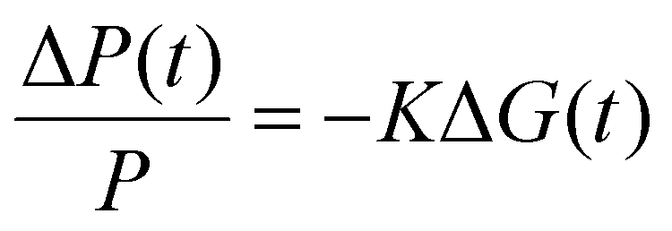 | (1) |
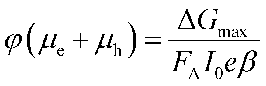
The TRMC signal is expressed in the product of mobility (μe + μh) and charge carrier yield φ, which was calculated from the maximum change in photoconductance ΔGmax:
 | (2) |
PLQY
Light from a laser diode (excitation wavelength = 523 nm) is coupled into a fibre directed into the integrating sphere and then, sample is illuminated. The emission from the sample is homogenized by multiple reflections within the integrating sphere and coupled out into another fibre that is connected to a spectrometer.Device performance
In-house current–voltage (JV) measurements were obtained on a temperature-controlled vacuum chuck at 25 °C, if not stated otherwise, using a two-lamp (halogen and xenon) class AAA WACOM sun simulator with an AM1.5G irradiance spectrum at 1000 W m−2. Shadow masks were used to define the illuminated area (here 0.1 cm2). The cells were measured with a scan rate of 100 mV s−1 (using an integration time of 0.02s and a delay of 0.02s for each data point).
Stability experiments
Accelerated ageing measurements for 40 h were performed with the advanced stability platform Litos by Fluxim AG, Switzerland. The samples were kept at 85 °C, illuminated by white LEDs at 1 sun-equivalent light intensity, and 12 pixels were kept at MPP. Standard stability tests were conducted in a customized environmental chamber (Cicci Research s.r.l.) under continuous nitrogen flow and at 35 °C for over 2000 h. Illumination was provided by an LED solar simulator calibrated to approximate AM1.5G, and the devices were at open-circuit condition.Author contributions
M. O., C. M. W. and A. H. W. conceived and designed the work. M. O. produced the original draft and all co-authors contributed to editing the manuscript. C. M. W., Q. J., A. H. W. and C. B. contributed to the investigation, methodology and analysis of the work. M. O. prepared the TEM specimens and collected the data. M. O., Q. J. and A. H. W. interpreted and analysed the SAED data. S. Z. and A.A. performed ultra-sensitive EQE measurements. S. T., S. E. and T. W. conducted and analysed the SIMS experiments. M. O. performed the AFM, KPFM and C-AFM experiments. M. O., C. M. W., D. A. J. and C. B. contributed to the planning and analysis of the AFM-analytical data. M. H. F. performed the potentiostatic polarization measurements. D. C. assisted in the analysis of the GIWAXS data. M. O. carried out the XRD experiments. M. O. fabricated the perovskite devices and carried out the stability tests. J. Z. and T. S. performed the TRMC measurements and provided the data analysis. C. M. W. and D. A. J. helped in analysing the spectroscopy data. A. J. and A. K. contributed to the analysis of the work. S. J., S. Z. and B. R. assisted in performing the accelerated device aging tests and contributed to the analysis of the work.Conflicts of interest
The authors declare no conflicts of interest.Acknowledgements
This project has received funding from the European Union's Horizon 2020 research and innovation programme (Marie Skłodowska-Curie grant agreement no. 945363, VIPERLAB, 101006715; TRIUMPH, 101075725), the Swiss National Science Foundation (PAPET, 200021_197006; A3P, 40B2-0_1203626), the Swiss Federal Office of Energy (PRESTO), and the ETH Domain through an AM grant (AMYS). M. H. F. is supported by a Rubicon Fellowship from the Netherlands Organisation for Scientific Research (NWO). A. A. acknowledges support from the Welsh Government's Sêr Cymru II Rising Star through the European Regional Development Fund, Welsh European Funding Office, and Swansea University Strategic Initiative in Sustainable Advanced Materials. The authors thank Dr Rita Therisod and Dr Victor Boureau of the Cimé for the support of the TEM experiments. The SIMS part of the work was funded by the Luxembourg National Research Fund (FNR) by the grant PRIDE17/12246511/PACE.References
- H. J. Snaith, Perovskites: The Emergence of a New Era for Low-Cost, High-Efficiency Solar Cells, J. Phys. Chem. Lett., 2013, 4, 3623–3630 CrossRef CAS.
- M. A. Green, A. Ho-Baillie and H. J. Snaith, The emergence of perovskite solar cells, Nat. Photonics, 2014, 8, 506–514 CrossRef CAS.
- S. N. Habisreutinger and M. O. Reese, Building perovskite solar cells that last, Science, 2022, 377, 265–266 CrossRef CAS PubMed.
- M. Grätzel, The light and shade of perovskite solar cells, Nat. Mater., 2014, 13, 838–842 CrossRef PubMed.
- J.-P. Correa-Baena, et al., Promises and challenges of perovskite solar cells, Science, 2017, 358, 739–744 CrossRef CAS PubMed.
- S. De Wolf, et al., Organometallic Halide Perovskites: Sharp Optical Absorption Edge and Its Relation to Photovoltaic Performance, J. Phys. Chem. Lett., 2014, 5, 1035–1039 CrossRef CAS PubMed.
- Best Research-Cell Efficiencies. (2023).
- G. E. Eperon, et al., Formamidinium lead trihalide: a broadly tunable perovskite for efficient planar heterojunction solar cells, Energy Environ. Sci., 2014, 7, 982–988 RSC.
- S.-H. Turren-Cruz, A. Hagfeldt and M. Saliba, Methylammonium-free, high-performance, and stable perovskite solar cells on a planar architecture, Science, 2018, 362, 449–453 CrossRef CAS PubMed.
- H. Lu, et al., Vapor-assisted deposition of highly efficient, stable black-phase FAPbI3 perovskite solar cells, Science, 2020, 370, eabb8985 CrossRef CAS PubMed.
- D. P. McMeekin, et al., A mixed-cation lead mixed-halide perovskite absorber for tandem solar cells, Science, 2016, 351, 151–155 CrossRef CAS PubMed.
- W. Shockley and H. J. Queisser, Detailed Balance Limit of Efficiency of p–n Junction Solar Cells, J. Appl. Phys., 1961, 32, 510–519 CrossRef CAS.
- O. J. Weber, et al., Phase Behavior and Polymorphism of Formamidinium Lead Iodide, Chem. Mater., 2018, 30, 3768–3778 CrossRef CAS.
- P. Gratia, et al., The Many Faces of Mixed Ion Perovskites: Unraveling and Understanding the Crystallization Process, ACS Energy Lett., 2017, 2, 2686–2693 CrossRef CAS.
- Z. Li, et al., Stabilizing Perovskite Structures by Tuning Tolerance Factor: Formation of Formamidinium and Cesium Lead Iodide Solid-State Alloys, Chem. Mater., 2016, 28, 284–292 CrossRef CAS.
- R. E. Beal, et al., Cesium Lead Halide Perovskites with Improved Stability for Tandem Solar Cells, J. Phys. Chem. Lett., 2016, 7, 746–751 CrossRef CAS PubMed.
- M. Saliba, et al., Cesium-containing triple cation perovskite solar cells: improved stability, reproducibility and high efficiency, Energy Environ. Sci., 2016, 9, 1989–1997 RSC.
- V. M. Goldschmidt, Die Gesetze der Krystallochemie, Naturwissenschaften, 1926, 14, 477–485 CrossRef CAS.
- C. Yi, et al., Entropic stabilization of mixed A-cation ABX3 metal halide perovskites for high performance perovskite solar cells, Energy Environ. Sci., 2016, 9, 656–662 RSC.
- Y. Bai, et al., Initializing film homogeneity to retard phase segregation for stable perovskite solar cells, Science, 2022, 378, 747–754 CrossRef CAS PubMed.
- T. A. S. Doherty, et al., Performance-limiting nanoscale trap clusters at grain junctions in halide perovskites, Nature, 2020, 580, 360–366 CrossRef CAS PubMed.
- T. A. S. Doherty, et al., Stabilized tilted-octahedra halide perovskites inhibit local formation of performance-limiting phases, Science, 2021, 374, 1598–1605 CrossRef CAS PubMed.
- K. Frohna, et al., Nanoscale chemical heterogeneity dominates the optoelectronic response of alloyed perovskite solar cells, Nat. Nanotechnol., 2022, 17, 190–196 CrossRef CAS PubMed.
- M. Othman, et al., Structural and Photophysical Properties of Guanidinium–Iodide-Treated Perovskite Solar Cells, Sol. RRL, 2023, 7, 2200852 CrossRef CAS.
- M. U. Rothmann, W. Li, J. Etheridge and Y.-B. Cheng, Microstructural Characterisations of Perovskite Solar Cells – From Grains to Interfaces: Techniques, Features, and Challenges, Adv. Energy Mater., 2017, 7, 1700912 CrossRef.
- D. P. McMeekin, et al., Crystallization Kinetics and Morphology Control of Formamidinium–Cesium Mixed-Cation Lead Mixed-Halide Perovskite via Tunability of the Colloidal Precursor Solution, Adv. Mater., 2017, 29, 1607039 CrossRef PubMed.
- W. Zhang, et al., Enhanced optoelectronic quality of perovskite thin films with hypophosphorous acid for planar heterojunction solar cells, Nat. Commun., 2015, 6, 1–9 CAS.
- J. Pan, et al., Room-Temperature, Hydrochloride-Assisted, One-Step Deposition for Highly Efficient and Air-Stable Perovskite Solar Cells, Adv. Mater., 2016, 28, 8309–8314 CrossRef CAS PubMed.
- P. Luo, et al., Fabrication of CsxFA1–xPbI3 Mixed-Cation Perovskites via Gas-Phase-Assisted Compositional Modulation for Efficient and Stable Photovoltaic Devices, ACS Appl. Mater. Interfaces, 2017, 9, 42708–42716 CrossRef CAS PubMed.
- B. Charles, et al., Phase Behavior and Substitution Limit of Mixed Cesium-Formamidinium Lead Triiodide Perovskites, Chem. Mater., 2020, 32, 2282–2291 CrossRef CAS.
- J. Yang, et al., Understanding the Role of Cesium on Chemical Complexity in Methylammonium-Free Metal Halide Perovskites, Adv. Energy Mater., 2023, 2202880 CrossRef CAS.
- H. Yuan, et al., Degradation of Methylammonium Lead Iodide Perovskite Structures through Light and Electron Beam Driven Ion Migration, J. Phys. Chem. Lett., 2016, 7, 561–566 CrossRef CAS PubMed.
- S. Macpherson, et al., Local nanoscale phase impurities are degradation sites in halide perovskites, Nature, 2022, 607, 294–300 CrossRef CAS PubMed.
- B. Conings, et al., Intrinsic Thermal Instability of Methylammonium Lead Trihalide Perovskite, Adv. Energy Mater., 2015, 5, 1–8 Search PubMed.
- B. Kim and S. I. Seok, Molecular aspects of organic cations affecting the humidity stability of perovskites, Energy Environ. Sci., 2020, 13, 805–820 RSC.
- Y. An, et al., Structural Stability of Formamidinium- and Cesium-Based Halide Perovskites, ACS Energy Lett., 2021, 6, 1942–1969 CrossRef CAS.
- W. Li, et al., The critical role of composition-dependent intragrain planar defects in the performance of MA1–xFAxPbI3 perovskite solar cells, Nat. Energy, 2021, 6, 624–632 CrossRef CAS.
- H. T. Pham, et al., Unraveling the influence of CsCl/MACl on the formation of nanotwins, stacking faults and cubic supercell structure in FA-based perovskite solar cells, Nano Energy, 2021, 87, 106226 CrossRef CAS.
- R. Guo, et al., Degradation mechanisms of perovskite solar cells under vacuum and one atmosphere of nitrogen, Nat. Energy, 2021, 6, 977–986 CrossRef CAS.
- B. Park, et al., Understanding how excess lead iodide precursor improves halide perovskite solar cell performance, Nat. Commun., 2018, 9, 3301 CrossRef PubMed.
- K. Gwisu, et al., Impact of strain relaxation on performance of α-formamidinium lead iodide perovskite solar cells, Science, 2020, 370, 108–112 CrossRef PubMed.
- M. M. Tavakoli, S. M. Zakeeruddin, M. Grätzel and Z. Fan, Large-Grain Tin-Rich Perovskite Films for Efficient Solar Cells via Metal Alloying Technique, Adv. Mater., 2018, 30, 1705998 CrossRef PubMed.
- J. Chen, et al., Origin of the high performance of perovskite solar cells with large grains, Appl. Phys. Lett., 2016, 108, 53302 CrossRef.
- W. Nie, et al., Solar cells. High-efficiency solution-processed perovskite solar cells with millimeter-scale grains, Science, 2015, 347, 522–525 CrossRef CAS PubMed.
- S. Jariwala, et al., Local Crystal Misorientation Influences Non-radiative Recombination in Halide Perovskites, Joule, 2019, 3, 3048–3060 CrossRef CAS.
- S. Zeiske, C. Kaiser, P. Meredith and A. Armin, Sensitivity of Sub-Bandgap External Quantum Efficiency Measurements of Solar Cells under Electrical and Light Bias, ACS Photonics, 2020, 7, 256–264 CrossRef CAS.
- S. Zeiske, et al., Static Disorder in Lead Halide Perovskites, J. Phys. Chem. Lett., 2022, 13, 7280–7285 CrossRef CAS PubMed.
- J. Warby, et al., Understanding Performance Limiting Interfacial Recombination in pin Perovskite Solar Cells, Adv. Energy Mater., 2022, 12, 2103567 CrossRef CAS.
- G. J. W. Aalbers, et al., Effect of sub-bandgap defects on radiative and non-radiative open-circuit voltage losses in perovskite solar cells, Nat. Commun., 2024, 15, 1–10 Search PubMed.
- W. H. M. Remmerswaal, et al., Quantifying Non-Radiative Recombination in Passivated Wide-Bandgap Metal Halide Perovskites Using Absolute Photoluminescence Spectroscopy, Adv. Energy Mater., 2024, 2303664, DOI:10.1002/AENM.202303664.
- C. Kaiser, et al., A universal Urbach rule for disordered organic semiconductors, Nat. Commun., 2021, 12, 3988 CrossRef CAS PubMed.
- C. Stecker, et al., Surface Defect Dynamics in Organic–Inorganic Hybrid Perovskites: From Mechanism to Interfacial Properties, ACS Nano, 2019, 13, 12127–12136 CrossRef CAS PubMed.
- M. Ledinsky, et al., Temperature Dependence of the Urbach Energy in Lead Iodide Perovskites, J. Phys. Chem. Lett., 2019, 10, 1368–1373 CrossRef CAS PubMed.
- F. Urbach, The Long-Wavelength Edge of Photographic Sensitivity and of the Electronic Absorption of Solids, Phys. Rev., 1953, 92, 1324 CrossRef CAS.
- E. Ugur, et al., Life on the Urbach Edge, J. Phys. Chem. Lett., 2022, 7702–7711, DOI:10.1021/acs.jpclett.2c01812.
- M. I. Saidaminov, et al., Multi-cation perovskites prevent carrier reflection from grain surfaces, Nat. Mater., 2020, 1–7, DOI:10.1038/s41563-019-0602-2.
- J. Sastre, et al., Blocking lithium dendrite growth in solid-state batteries with an ultrathin amorphous Li–La–Zr–O solid electrolyte, Commun. Mater., 2021, 2, 76 CrossRef CAS.
- M. H. Futscher, M. K. Gangishetty, D. N. Congreve and B. Ehrler, Quantifying mobile ions and electronic defects in perovskite-based devices with temperature-dependent capacitance measurements: Frequency vs time domain, J. Chem. Phys., 2020, 152, 044202 CrossRef CAS PubMed.
- E. M. Hutter, et al., Thermodynamic Stabilization of Mixed-Halide Perovskites against Phase Segregation, Cell Rep. Phys. Sci., 2020, 1, 100120 CrossRef CAS.
- D. Gu, S. K. Dey and P. Majhi, Effective work function of Pt, Pd, and Re on atomic layer deposited HfO2, Appl. Phys. Lett., 2006, 89, 82907 CrossRef.
- M. Othman, et al., Millimeter-Sized Clusters of Triple Cation Perovskite Enables Highly Efficient and Reproducible Roll-to-Roll Fabricated Inverted Perovskite Solar Cells, Adv. Funct. Mater., 2022, 2110700 CrossRef CAS.
- E. Aydin, et al., Ligand-bridged charge extraction and enhanced quantum efficiency enable efficient n–i–p perovskite/silicon tandem solar cells, Energy Environ. Sci., 2021, 14, 4377–4390 RSC.
- S. Y. Leblebici, et al., Facet-dependent photovoltaic efficiency variations in single grains of hybrid halide perovskite, Nat. Energy, 2016, 1, 16093 CrossRef CAS.
- D. W. de Quilettes, et al., Impact of microstructure on local carrier lifetime in perovskite solar cells, Science, 2015, 348, 683–686 CrossRef CAS PubMed.
- D. H. Kim, et al., 300% Enhancement of Carrier Mobility in Uniaxial-Oriented Perovskite Films Formed by Topotactic-Oriented Attachment, Adv. Mater., 2017, 29, 1606831 CrossRef PubMed.
- L. Oesinghaus, et al., Toward Tailored Film Morphologies: The Origin of Crystal Orientation in Hybrid Perovskite Thin Films, Adv. Mater. Interfaces, 2016, 3, 1600403 CrossRef.
- J. Warby, et al., Mismatch of Quasi–Fermi Level Splitting and Voc in Perovskite Solar Cells, Adv. Energy Mater., 2023, 2303135 CrossRef CAS.
- K. A. Elmestekawy, et al., Photovoltaic Performance of FAPbI3 Perovskite Is Hampered by Intrinsic Quantum Confinement, ACS Energy Lett., 2023, 8, 2543–2551 CrossRef CAS PubMed.
- K. A. Elmestekawy, et al., Controlling Intrinsic Quantum Confinement in Formamidinium Lead Triiodide Perovskite through Cs Substitution, ACS Nano, 2022, 16, 9640–9650 CrossRef CAS PubMed.
- A. D. Wright, et al., Intrinsic quantum confinement in formamidinium lead triiodide perovskite, Nat. Mater., 2020, 19, 1201–1206 CrossRef CAS PubMed.
- K. Domanski, E. A. Alharbi, A. Hagfeldt, M. Grätzel and W. Tress, Systematic investigation of the impact of operation conditions on the degradation behaviour of perovskite solar cells, Nat. Energy, 2018, 3, 61–67 CrossRef CAS.
- F. Fu, et al., I2 vapor-induced degradation of formamidinium lead iodide based perovskite solar cells under heat–light soaking conditions, Energy Environ. Sci., 2019, 12, 3074–3088 RSC.
- M. V. Khenkin, et al., Consensus statement for stability assessment and reporting for perovskite photovoltaics based on ISOS procedures, Nat. Energy, 2020, 5, 35–49 CrossRef.
- T. Wirtz, O. De Castro, J.-N. Audinot and P. Philipp, Imaging and Analytics on the Helium Ion Microscope, Annu. Rev. Anal. Chem., 2019, 12, 523–543 CrossRef CAS PubMed.
- V. Dyadkin, P. Pattison, V. Dmitriev and D. Chernyshov, A new multipurpose diffractometer PILATUS@SNBL, J. Synchrotron Radiat., 2016, 23, 825–829 CrossRef CAS PubMed.
- D. Chernyshov, I. Dovgaliuk, V. Dyadkin and W. van Beek, Principal Component Analysis (PCA) for Powder Diffraction Data: Towards Unblinded Applications, Crystals, 2020, 10, 581 CrossRef CAS.
Footnote |
| † Electronic supplementary information (ESI) available. See DOI: https://doi.org/10.1039/d4ee00901k |
| This journal is © The Royal Society of Chemistry 2024 |