
 Open Access Article
 This Open Access Article is licensed under a
 Creative Commons Attribution 3.0 Unported Licence
Triple-junction perovskite–perovskite–silicon solar cells with power conversion efficiency of 24.4%†
Hang
Hu
ab,
Sophie X.
An
b,
Yang
Li
ab,
Seyedamir
Orooji
 ab,
Roja
Singh
ab,
Fabian
Schackmar
ab,
Felix
Laufer
ab,
Qihao
Jin
b,
Thomas
Feeney
ab,
Alexander
Diercks
b,
Fabrizio
Gota
ab,
Somayeh
Moghadamzadeh
ab,
Ting
Pan
ab,
Michael
Rienäcker
c,
Robby
Peibst
cd,
Bahram Abdollahi
Nejand
*ab and
Ulrich W.
Paetzold
*ab
ab,
Roja
Singh
ab,
Fabian
Schackmar
ab,
Felix
Laufer
ab,
Qihao
Jin
b,
Thomas
Feeney
ab,
Alexander
Diercks
b,
Fabrizio
Gota
ab,
Somayeh
Moghadamzadeh
ab,
Ting
Pan
ab,
Michael
Rienäcker
c,
Robby
Peibst
cd,
Bahram Abdollahi
Nejand
*ab and
Ulrich W.
Paetzold
*ab
aInstitute of Microstructure Technology (IMT), Karlsruhe Institute of Technology (KIT), Hermann-von-Helmholtz-Platz 1, 76344 Eggenstein-Leopoldshafen, Germany. E-mail: bahram.abdollahi@kit.edu; ulrich.paetzold@kit.edu
bLight Technology Institute (LTI), Karlsruhe Institute of Technology (KIT), Engesserstrasse 13, 76131 Karlsruhe, Germany
cInstitute for Solar Energy Research Hamelin (ISFH), Am Ohrberg 1, 31860, Emmerthal, Germany
dInstitute of Electronic Materials and Devices, Leibniz Universität Hannover, Schneiderberg 32, 30167, Hannover, Germany
First published on 13th February 2024
Abstract
The recent tremendous progress in monolithic perovskite-based double-junction solar cells is just the start of a new era of ultra-high-efficiency multi-junction photovoltaics. We report on triple-junction perovskite–perovskite–silicon solar cells with a record power conversion efficiency of 24.4%. Optimizing the light management of each perovskite sub-cell (∼1.84 and ∼1.52 eV for top and middle cells, respectively), we maximize the current generation up to 11.6 mA cm−2. Key to this achievement was our development of a high-performance middle perovskite sub-cell, employing a stable pure-α-phase high-quality formamidinium lead iodide perovskite thin film (free of wrinkles, cracks, and pinholes). This enables a high open-circuit voltage of 2.84 V in a triple junction. Non-encapsulated triple-junction devices retain up to 96.6% of their initial efficiency if stored in the dark at 85 °C for 1081 h.
Broader contextMetal halide perovskite semiconductors are the prime candidate for next generation of ultra-high-efficiency multi-junction photovoltaics (PVs) using three or even more junctions. However, triple-junction PVs (e.g., perovskite–perovskite–silicon) lag far behind in performance with only very few reports on prototypes. One of the key challenges in processing triple junction to date is the most critical junction, i.e., middle perovskite sub-cell, since it is processed on top of the silicon bottom cell and needs to withstand the subsequent processing of the wide-bandgap perovskite top cell. This work presents key advances on triple-junction perovskite–perovskite–silicon solar cells with a record efficiency of 24.4%. Key achievements are developing a stable pure-α-phase high-quality middle perovskite thin film and optimizing the light management of each perovskite sub-cell. This work opens the door to a new era of perovskite-based high-efficiency triple-junction PVs. |
Introduction
Recent advancements in power conversion efficiencies (PCEs) of monolithic perovskite-based double-junction solar cells1–8 denote just the start of a new era in ultra-high-efficiency multi-junction photovoltaics (PVs) using three or even more junctions. Such devices will surpass by far the detailed-balanced limit in PCE for single-junction devices9 and might even compete at one stage with triple- and six-junction solar cells based on epitaxially grown III–V crystalline semiconductor thin films,1,10 given the bandgap tunability, excellent optoelectronic characteristics, and low-cost facile process of perovskite material class.11,12 Incorporation of a third sub-cell into a double-junction stack, i.e., triple-junction architecture, can further increase energy yield (e.g., reducing thermalization loss).9,11,13 The detailed balance limit for triple-junction PVs of 51% (compared to ∼45% for double junctions) sets the ultimate boundary and shows the headroom for next-generation perovskite-based multi-junction PVs.14,15 However, as high-performance perovskite semiconductors are only available today for bandgaps down to ∼1.25 eV,1,6–8 monolithic perovskite-based multi-junctions will need to be combined with a narrow bandgap silicon (Si) or a copper indium (gallium) selenide bottom solar cell – e.g., in a perovskite–perovskite–Si architecture – to exploit the solar spectrum efficiently.To reach these high performances, several challenges need to be addressed, such as the sequential processing of high-quality perovskite thin films in the increasingly complex multi-layer architecture, light management, and current matching of the monolithically interconnected sub-cells, as well as the development of low-loss tunnel/recombination junctions. Optical modeling reveals potential in PCEs of up to 36.6% and 38.8% for all-perovskite and perovskite–perovskite–Si monolithic triple-junction solar cells (MTJSCs), respectively.11 However, the experimental realization lags far behind and, to date, only very few prototypes of all-perovskite14,16–19 or perovskite-perovskite–Si MTJSCs12,15,20,21 were demonstrated, reaching maximum PCEs of 25.1%19 and 22.2%,20 respectively. The device performances of perovskite–perovskite–Si MTJSCs were limited with imperfect recombination junction between perovskite sub-cells (i.e., either low fill factor (FF) or low open-circuit voltage (VOC))12 or low current generation in the middle perovskite sub-cell (i.e., low short-circuit current density (JSC) <10.2 mA cm−2).12,15,20,21 It is highlighted that to date the most critical junction in the sequential processing of perovskite–perovskite–Si MTJSC is the middle-bandgap (MBG) perovskite sub-cell, since it is processed on top of the Si bottom cell and needs to withstand the subsequent processing of the wide-bandgap (WBG) perovskite top cell. The middle perovskite sub-cell is required to provide (i) a suitable MBG, (ii) very good thermal stability, (iii) excellent interfaces to both recombination junctions, and (iv) a low density of defects and pinholes. Optical modeling and simulations predict that MBG perovskite with a bandgap of 1.40–1.50 eV is favored to maximize JSC in a triple-junction perovskite–perovskite–Si architecture.11,12 We note that – to date – high-quality perovskite thin films with bandgaps <1.50 eV rely on unstable mixed Sn/Pb-based compositions that degrade swiftly if exposed to minimal amounts of oxygen and water.6,7 For this reason, only Pb-based compositions of CsxFAyMA1−x−yPb(IzBr1−z)3 (Cs: cesium; FA: formamidinium; MA: methylammonium; Pb: lead; I: iodide; Br: bromide) were used in perovskite–perovskite–Si MTJSCs.12,15,20,21 The most promising candidate for a high-efficiency and reasonably stable MBG perovskite thin film is FAPbI3, which exhibits an optical bandgap of ∼1.52 eV22–24 (desired for (i)). Single-junction FAPbI3 perovskite solar cells have demonstrated excellent device performance and offer good thermal stability22–28 (addressing (ii)) but have not yet been employed in multi-junction PVs. Moreover, (iii) and (iv) are crucial to prevent degradation of the multi-layer thin-film stacks during subsequent solution-based processing of the WBG perovskite top solar cell (see our previous reports of all-perovskite double-junction modules7). Since conventional anti-solvent (AS) quenching methods are reported to induce surface wrinkles, micro-cracks, and/or pinholes,29–32 as well as high density of defects at the perovskite/electron transport layer (ETL) interface,32,33 an alternative AS-free quenching method for processing the MBG perovskite thin film is highly encouraged.
In this work, we present high-efficiency perovskite–perovskite–Si MTJSCs using a Cs0.2FA0.8Pb(I0.5Br0.5)3 WBG perovskite top cell (∼1.84 eV), a FAPbI3 perovskite middle cell (∼1.52 eV), and a Si bottom cell (∼1.1 eV). Our champion device achieves an unprecedented PCE of 24.4%, which is, to our knowledge, the highest PCE (active area of ∼0.5 cm2) reported for this architecture. Via optimizing light management and maximizing the photocurrent of the perovskite sub-cells, we further improve the JSC up to 11.6 mA cm−2, which exceeds previous reports.12,15,20,21 Importantly, using a vacuum-assisted growth (VAG) control, we process high-quality (free of wrinkles, pinholes, and cracks) and phase-stable FAPbI3 middle perovskite sub-cell. Our perovskite–perovskite–Si solar cells demonstrate high VOC up to 2.84 V, given high-quality thin films and low non-radiative recombination loss at the perovskite/ETL interfaces. Moreover, non-encapsulated triple-junction solar cells show good thermal stability and retain 96.6% of initial PCE if stored in an N2 atmosphere at 85 C for 1081 h.
Results and discussion
Simulations of perovskite–perovskite–Si MTJSCs
To maximize the overall JSC in our perovskite–perovskite–Si triple-junction architecture, we perform numerical simulations with the target to minimize parasitic absorption and reflection losses and to identify the optimal combination of bandgaps as well as thicknesses of the perovskite thin films for the top and middle sub-cells (the bandgap of the Si bottom cell is fixed ∼1.1 eV, Fig. 1(a)). The device architecture is based on prototypes reported in literature with realistic experimental data (see experimental procedures for details) and established material combinations used in our previous work for double-junction architectures.7,34,35 Our simulations predict – for the perovskite–perovskite–Si triple-junction architecture under study (Fig. 1(a)) – a maximum PCE of 24.8% for the ideal bandgap combination of ∼1.82 eV and ∼1.48 eV of the top and middle perovskite sub-cells, respectively (Fig. 1(b) and Fig. S1, S2, ESI†). Previous reports on perovskite–perovskite–Si MTJSCs applied bandgap combinations that differ significantly for this optimum. For instance, Zheng et al. reported in 2022 a PCE of 20.1% with a JSC of 8.5 mA cm−2 using a bandgap combination of 1.55 eV and 1.90 eV,15 and Choi et al. latest reported a PCE of 22.2% with a JSC of 10.19 mA cm−2 using a bandgap combination of 1.56 eV and 1.96 eV.20 The current generation in these devices was constrained by the middle sub-cell. As discussed above, except for Sn/Pb mixed perovskite compositions, we compromise in this study to a small extent on the maximum achievable efficiency, thereby extending the range of suitable bandgap combinations. FAPbI3 provides a suitable optical bandgap ∼1.52 eV25–28 (∼1.48 eV is also reported as an ideal bandgap of pure black cubic α-phase FAPbI322–24 which is very close to our optimal simulated value), excellent performance, and thermal stability in single-junction devices.22–28 We note that good charge carrier extraction was achieved in our previous experimental studies for perovskite solar cells based on up to ∼600 nm thick planar FAPbI3 absorber.36 According to our simulations, the ideal counterpart for a >600 nm thick FAPbI3 middle sub-cell is a perovskite top sub-cell with a WBG of ∼1.84 eV (Fig. 1(c) and Fig. S3–S5, ESI†) and an absorber thickness of ∼200 nm. The thinner (<200 nm) or thicker (>300 nm) WBG perovskite layer of the top cell would result in a significant current mismatch between these two perovskite sub-cells, i.e., as a consequence of an overall JSC < 10 mA cm−2 and significant loss in PCE (see Fig. S4 and S5, ESI†). Fig. 1(d) shows a close to perfect current matching between the top and middle cub-cells in the champion simulated perovskite (∼1.84 eV)–perovskite (∼1.52 eV)–Si (∼1.1 eV) MTJSCs. The simulated integrated photocurrent densities are 12.0, 11.7, and 15.4 mA cm−2 for the top, middle, and bottom sub-cells, respectively (Fig. 1(d)). The parasitic absorption and reflection losses could be minimized to 7.2 mA cm−2 in total. The latter leaves room for improvement in future works. | ||
| Fig. 1 Simulations of perovskite–perovskite–Si MTJSCs. (a) Illustration of triple-junction concept. Contour plots of simulated PCEs of perovskite–perovskite–Si MTJSCs for (b) varied bandgap combinations of top/middle perovskites and (c) varied thickness of top (1.84 eV) and middle (1.52 eV) perovskites. In (b), the black stars indicate experimental PCEs from the reports,12,15,20,21 and the white dot (star) indicates simulated (experimental) PCEs from this work. (d) Simulated EQE spectra for the MTJSC combined with perovskite bandgaps of 1.84 eV and 1.52 eV. The parasitic absorption and reflection losses are calculated to be 2.8 mA cm−2 and 4.4 mA cm−2, respectively. | ||
PV performance of perovskite–perovskite–Si MTJSCs
Perovskite–perovskite–Si MTJSCs were fabricated according to the above-described rationale (see Fig. 2(a)). The layer stack of the top and middle junction perovskite solar cells was processed on top of a ∼200-μm-thick potassium hydroxide-etched Si bottom solar cell (with passivating electron-selective full-area front and hole-selective-partial textured rear contacts based on a doped polysilicon-on-oxide (POLO) contact scheme). The entire layer stack of middle and top perovskite sub-cells is indium tin oxide (ITO)/nickel oxide (NiOx)/[2-(9H-carbazol-9-yl)ethyl]phosphonic acid (2PACz)/FAPbI3/fullerene (C60)/tin oxide (SnOx)/ITO/NiOx/2PACz/Cs0.2FA0.8Pb(I0.5Br0.5)3/lithium fluoride (LiF)/C60/SnOx/indium zinc oxide (IZO)/gold (Au)/magnesium fluoride (MgF2). Fig. 2(b) shows the triple-junction solar cell's cross-sectional scanning electron microscopy (SEM) image. For the middle and top perovskite sub-cells, perovskite thin films with the nominal compositions of FAPbI3 (∼1.52 eV, see Fig. S6, ESI;† ∼650 nm) and Cs0.2FA0.8Pb(I0.5Br0.5)3 (∼1.84 eV, see Fig. S7, ESI;† ∼200 nm) were applied, respectively. The recombination junctions are formed by sputtered ITO layers (15–20 nm). We note that ITO also serves as anchoring oxide for the sequential hole transport layer (HTL), especially for the double HTLs of NiOx/self-assembled monolayer (SAM).3 A double HTLs based on a combination of sputtered NiOx and 2PACz is used in both perovskite subcells, offering an excellent charge carrier extraction, a robust barrier for the solvents of perovskite precursor, and a very good yield for the devices.12,15,17 Our champion device provides a PCE of 24.4% (backward scan, VOC: 2.84 V, JSC: 11.6 mA cm−2, FF: 0.74) with negligible hysteresis in current-density–voltage (J–V) characteristics (see Fig. 2(c)). After 5 min of continuous maximum power point (MPP) tracking under continuous AM 1.5G (100 mW cm−2) irradiation the solar cell shows 24.1% (Fig. 2(d)) of PCE. To our knowledge, this is the highest reported PCE for perovskite–perovskite–Si MTJSCs. We highlight that the perovskite layer of the middle sub-cell is processed with the VAG strategy in this work, enabling higher PV performance and yield in triple junctions compared to using a conventional AS method (see Fig. S8 and S9, ESI,† backward scan, PCE: 15.9%, VOC: 2.65 V, JSC: 10.9 mA cm−2, FF: 0.55). Our champion perovskite–perovskite–Si MTJSC exhibits a similar external quantum efficiency (EQE) to the simulated optimum (Fig. 1(d)) with integrated photocurrent densities of 11.6, 11.0, and 15.9 mA cm−2 for the top perovskite sub-cell (∼1.84 eV), the middle perovskite sub-cell (∼1.52 eV), and the Si bottom sub solar cell (∼1.1 eV) (see Fig. 2(e)), respectively. Given the low-loss transparent and conductive oxide front electrode (TCO, Fig. S10a, ESI†) and the optimized antireflection coating (using MgF2, Fig. S10b and c, ESI†) layers the device shows low absorption losses (corresponding photocurrent density ∼5.9 mA cm−2, Fig. 2(e)) and reflection losses (corresponding photocurrent density ∼2.2 mA cm−2, Fig. 2(e)). We highlight that the remarkable device performance of our MTJSCs stands out from the very few previous reports for this type of solar cells (Fig. 2(f)). Our device exceeds previous prototypes of perovskite–perovskite–Si MTJSCs in JSC (Fig. 2(f)). | ||
| Fig. 2 PV performance of perovskite–perovskite–Si MTJSCs. (a) Schematic and (b) cross-section SEM image of perovskite–perovskite–Si triple-junction architecture. (c) J–V characteristics of forward and backward scans, (d) stabilized PCE under continuous AM 1.5G illumination, and (e) EQE spectra of a champion perovskite–perovskite–Si MTJSC. The parasitic absorption and reflection losses are calculated to be 5.9 mA cm−2 and 2.2 mA cm−2, respectively. (f) Summary of reported perovskite-based MTJSCs.12,14–21 | ||
The major challenge in processing the entire stack of our MTJSCs arises from the large number of subsequent layer depositions. While most of the layers in our architecture are processed by physical vapor deposition, which allows for controlled conformal deposition of thin films, the perovskite absorber layers are spin-coated. To avoid a penetration of the solvents (dimethylformamide (DMF)/dimethyl sulfoxide (DMSO)) and anti-solvents (ethyl acetate (EA)) in the underlying layers of the device architecture and to allow for the processing of pinhole-free perovskite thin films, we employ the VAG strategy established in our team for the processing of all-perovskite double-junction solar cells6,7 and high-quality FAPbI3 thin films.36 VAG process achieves a significantly higher performance (Fig. S11, ESI†) in a semitransparent single-junction middle cell (PCE: 20.0%, VOC: 1.08 V, FF: 0.84, JSC: 22.0 mA cm−2) compared to AS method (PCE: 13.9%, VOC: 1.00 V, FF: 0.66, JSC: 21.1 mA cm−2). The thickness of MBG FAPbI3 thin films is optimized (up to ∼650 nm) by controlling the concentration of perovskite precursor (i.e., optimum 1.3 M, see Fig. 2(b)). A thinner MBG perovskite layer leads to insufficient light absorbing, resulting in a lower JSC (see Fig. S12, ESI†) in single junction as well as a current mismatch in triple junctions (Fig. S13, ESI†). A thicker MBG perovskite layer impacts the charge extraction. It leads to the increased non-radiative recombination,37 which impacts VOC and FF (see Fig. S12, ESI†) and leads to a current mismatch in triple junction (Fig. S13a and b, ESI†). Compared to the AS method, the increase in JSC in the VAG-processed middle cell is pivotal to realizing a good current match between the top and middle sub-cells in the triple-junction architecture (Fig. 2(e) and Fig. S13, S10, S11b, and c, ESI†). We attribute the VOC enhancement in the middle sub-cell processed by VAG to the reduced non-radiative recombination loss, which is discussed later.
For the top cell, the thickness of WBG perovskite is optimized to ∼200 nm (Fig. 2(b) and Fig. S4, S5, and S13, ESI†) in triple junctions. We find that AS and VAG methods deliver similar PV performance in the semitransparent architecture of the top cell (Fig. S14 and S15, ESI†). We hypothesize that (i) the faster nucleation/crystallization of the Br-rich WBG perovskites thin film38 and/or (ii) the promotion of the photoactive (black) phase formation due to the presence of Br− during the nucleation39 facilitates the formation of WBG perovskite thin film compared to MBG perovskite thin film. Future studies on the perovskite thin film formation during the AS and VAG methods for processing high-performance WBG perovskite PVs are required to shed light on this subject, and we believe that novel in situ characterization methods will be valuable tools to study these aspects.
Morphology and phase stability of middle perovskite thin films
The quality of the perovskite thin films, i.e., the middle-junction FAPbI3, is decisive for the performance.29,32 In this regard, we examine the morphology of FAPbI3 thin films fabricated by AS and VAG methods (referred to as AS-FAPbI3 and VAG-FAPbI3) and the sequential layers with C60 and SnOx (i.e., the layer stack of AS-FAPbI3/C60/SnOx and VAG-FAPbI3/C60/SnOx). We observe micro-wrinkles throughout the surface of AS-FAPbI3 and AS-FAPbI3/C60/SnOx thin films, as shown in the microscopic and SEM images (Fig. 3(a) and (b)). Such surface wrinkles have been reported in the processing of a wide range of perovskite thin films.29–32 They are caused by the relaxation of the compressive strain during perovskite crystallization.29–31,33 Since the thermal expansion coefficient for TCO or glass substrate is one order of magnitude lower than perovskite and organic thin films,40 the substrate (i.e., Si substrate/ITO/NiOx/2PACz layer stack in this work) constraints the perovskite volume expansion during the intermediate phase formation, resulting in energy release of compressive strain. In the AS quenching process, the anti-solvent (i.e., EA) assists in removing solvents (i.e., DMF/DMSO), but the extraction rate is not sufficient during the formation of an intermediate-phase thin film, resulting in compressive strain release.30 In contrast, during the VAG process, the prompt extraction and well-controlled removal of precursor solvents (i.e., DMF/DMSO) lead to a faster formation intermediate phase41,42 (i.e., the intermediate phase is formed after ∼20 s during the VAG process, optimal vacuum time: 30 s). After post-annealing, less solvent releases or less perovskite volume changes between the perovskite thin film and the underlying substrate, resulting in less or free residual strain.33 The remaining cracks (Fig. 3(b) and Fig. S16, ESI†) in AS-FAPbI3/C60/SnOx stack indicate significant residual strain releasing during the temperature-dependent atomic layer deposition of SnOx thin film (ALD-SnOx, i.e., 90 °C deposition for 2.5 h for ∼30 nm5,7 in this work). Notably, the pinholes or cracks observed in AS-FAPbI3 thin film (Fig. S17, ESI†) allow for faster penetration of the solvents of the WBG perovskite7 (Fig. S18, ESI†), resulting in non-radiative recombination centers33 or shunting in a single-junction as well as a triple-junction architecture (see Fig. S8, ESI†). | ||
| Fig. 3 Morphology and phase stability of middle perovskite thin films. (a) Top-view optical microscopic and (b) SEM images of middle perovskite thin films and sequential deposition of C60 and SnOx layers. FAPbI3 perovskite thin films were fabricated with VAG and AS methods. (c) XRD patterns and (d) the corresponding full width at half maximum (FWHM). The XRD intensity ratios of (e) δ-phase/(001) plane and (f) PbI2/(001) plane for FAPbI3 thin films and FAPbI3/C60/SnOx stack. | ||
One of the aims of using the VAG process is to obtain stable α-phase FAPbI3 thin films. X-ray diffraction (XRD) patterns confirm α-phase formed in FAPbI3 thin films43 for both routes of fabrication (Fig. 3(c)). Compared to AS-FAPbI3 thin films, the reduction of full width at half maximum (FWHM) observed in all VAG-FAPbI3 thin films (even after deposition of C60/SnOx layers) reflects a larger size of crystallites (Fig. 3(d) and Fig. S19, ESI†). Most importantly, the yellow orthorhombic phase (δ-FAPbI3) emerges in AS-FAPbI3 thin film (Fig. 3(c)), and α-to-δ phase transition occurs (Fig. 3(e)) after sequential deposition of C60/SnOx, as the ratio of δ/(001) increases further (almost double). The residual strain may induce a pronounced α-to-δ phase transition as the cracks and wrinkles are still found in the AS-FAPbI3/C60/SnOx stack (see Fig. 3(a) and (b)).26,44,45 The strain releasing in AS-FAPbI3 thin film during the ALD process causes cracks in the C60 layer as well, generating a penetration pathway for diffusion of the tetrakis(dimethylamino)tin(IV) precursor during ALD-SnOx deposition and consequently reaction with AS-FAPbI3 layer. In contrast, FAPbI3 thin films fabricated by VAG process remain pure α phase before and after sequential deposition, demonstrating superior phase stability. Furthermore, an apparent PbI2 peak is found in all FAPbI3 thin films (Fig. 3(f)) as 10 mol% of excess PbI2 is utilized as a standard recipe in this work, which has been reported in many FA-based perovskite solar cells with a p–i–n architecture.36,46,47 The peak ratio of PbI2/(001) retains ∼11% for both of VAG-FAPbI3 thin film and VAG-FAPbI3/C60/SnOx stack, whereas AS-FAPbI3/C60/SnOx stack delivers an increased ratio from ∼13% to >20%. This reveals no degradation in the VAG process and during sequential layer depositions (especially in the ALD process) but accelerated degradation to PbI2 for AS-FAPbI3 thin film during the ALD process that may also be caused by the residual strain.44
In brief, the VAG process enables high-quality and stable pure-α-phase MBG FAPbI3 thin films. This provides an ideal substrate for two sequential rounds of the ALD-SnOx process to protect the MBG perovskite against the high-energy sputtering for recombination junction (Fig. 3(a), (b) and Fig. S16, S17, ESI†), against solvent corrosion (i.e., degradation or dissolution, Fig. S18, ESI†) for WBG (1.84 eV) processing, and high-temperature post annealing (e.g., ∼150 °C for WBG). This enhancement contributes to high PV performance in a triple-junction architecture (Fig. 2).
Characteristics of non-radiative recombination for middle sub-cell
To elucidate the origin of the VOC improvement (e.g., in the perovskite bulk or/and at the interfaces), we investigate the middle perovskite thin films and single-junction devices with following three architectures: (i) a half stack of ITO/2PACz/FAPbI3, (ii) a whole stack of ITO/2PACz/FAPbI3/C60/SnOx, and (iii) full opaque or semitransparent device.We perform time-resolved photoluminescence (TRPL) and photoluminescence quantum yield (PLQY) measurements on stacks (i) and (ii). The stack (i) processed with both VAG and AS shows a mono-exponential decay in TRPL (Fig. 4(a)). VAG process exhibits a slightly increased charge-carrier lifetime (τ = 3581 ns) compared to AS method (τ = 3313 ns), which can be attributed to the improved grain size with fewer grain boundaries and free pinholes in VAG-FAPbI3 thin film (Fig. 3(b)) and pure-α-phase (Fig. 3(c) and (e)).6,28,48 The comparable average values of PLQY and implied open-circuit voltage (VOC-imp)47,49 (VAG: 2.5 × 10⁻², 1.135 V; AS: 2.0 × 10⁻², 1.129 V; see Fig. 4(b)) indicate negligible non-radiative recombination loss from the bulk and 2PACz/FAPbI3 interface. Stack (ii) shows a biexponential decay with a fast (τ1) and a slow lifetime (τ2) in TRPL (Fig. 4(a), Table S1, ESI†). The minimal values of τ1 (AS: 3 s; VAG: 4 s) in both fabrication methods reveal a very fast charge transfer from FAPbI3 to C60/SnOx (Table S1, ESI†). Compared to AS method, a longer τ2 for VAG process (27 ns vs. 16 ns, Fig. 4(a)) demonstrates less non-radiative recombination at FAPbI3 and C60/SnOx interface.6,28,48 We realize the main VOC loss is related to the interface of FAPbI3 and C60/SnOx since the PLQY decreases in the stack (ii) (VAG: from 2.5 × 10⁻² to 1.2 × 10⁻³; AS: from 2.0 × 10⁻² to 3.9 × 10⁻⁵, Fig. 4(b)). The corresponding average values of VOC-imp decrease to 1.056 V for VAG process and 0.969 V for AS process, respectively. Importantly, the VOC-imp loss at FAPbI3 and C60/SnOx interface is reduced to 0.079 V for the VAG process, compared to that of 0.160 V for AS method (Fig. 4(b)). This matches well with the difference in VOC (VAG: 1.08 V; AS: 1.00 V, Fig. S11a, ESI†). In addition, we find ALD temperature (90 °C for ∼150 min) does not affect the quality of FAPbI3 thin films as the PLYQ and VOC-imp slightly increased after the samples of ITO/2PACz/FAPbI3 were heated up at the same condition (Fig. 4(b)).
 | ||
| Fig. 4 Characteristics of non-radiative recombination for middle sub-cell. (a) TRPLs and (b) PLQYs for ITO/2PACz/FAPbI3 and ITO/2PACz/FAPbI3/C60/SnOx stacks. (c) EL imaging of opaque and semitransparent single-junction FAPbI3-based devices. (d) Trap density obtained from the SCLC method, (e) light intensity dependence of the VOC, and (f) normalized transient photovoltage decay of semitransparent FAPbI3-based devices. | ||
We propose that a high trap density could originate from the defects at the interface of FAPbI3 and C60/SnOx due to poor perovskite film quality and unstable α phase, thus resulting in a substantial trap-assisted non-radiative recombination.3,50 We utilize electroluminescence (EL) imaging on opaque and semitransparent devices to evaluate the defect distribution and film homogeneity. The EL signal increases with the local junction voltage, so the dark regions show local defects.7,51,52 As shown in Fig. 4(c), the devices processed with the VAG method present good homogeneity with significantly fewer defects. In contrast, the devices fabricated by the AS method show many local defects. In combination with the analyses of TRPL and PLQY (see Fig. 4(a) and (b)), we hypothesize these defects may mainly generate from the interfacial pinholes, cracks, inactive δ-phase, or wrinkles (e.g., different local defect density in the hill or valley29) after the deposition of ETL. We further estimate the trap density (nt) employing space-charge-limited-current (SCLC) method.6,28,53–55 The nt (Fig. 4(d) and Fig. S20a, ESI†) for VAG device (5.32 × 1015 cm−3) is less than a half compared to AS devices (11.22 × 1015 cm−3), demonstrating significantly reduced trap-assisted non-radiative recombination at the interface of FAPbI3 and C60/SnOx. We further investigate semitransparent devices utilizing light intensity dependence of the VOC and transient photovoltage (TPV) characterizations. A lower ideality factor (nid; VAG: 1.12; AS: 1.44; Fig. 4(e)) and longer charge-recombination lifetime (VAG: 4.52 μs; AS: 2.63 μs; Fig. 4(f)) indicate that the charge recombination pathways in VAG device are efficiently blocked.56,57 This conclusion is further supported by reduced dark saturation current density (Fig. S20b, ESI†), a higher flat-band potential in Mott–Schottky plots (Fig. S20c, ESI†), and a higher charge recombination resistance in electrochemical impedance spectroscopy measurements (Fig. S20d and Table S2, ESI†), as they are in line with the data of TRPL, PLQY, SCLC, nid, and TPV (Fig. 4).
Overall, we demonstrate high-performance middle sub-cell by applying high-quality MBG FAPbI3 thin film is the key advance on triple-junction perovskite–perovskite–silicon solar cells. Compared to the optimum simulated VOC (2.95 V, see simulation in Experimental procedures), there is still room to further reduce the VOC loss in middle and top perovskite sub-cells.
Durability of perovskite–perovskite–Si MTJSCs
Eventually, we evaluate the durability of our non-encapsulated perovskite–perovskite–Si MTJSCs in a N2 atmosphere. The stabilities of AS and VAG devices are first examined with MPP tracking under continuous AM 1.5G illumination (100 mW cm−2) at ∼50 °C (Fig. 5(a)). After 11 h, the VAG device retains 96% of initial PCE, which is more stable than AS device retaining 89% of the initial PCE. The slight drop in PCE of the champion triple-junction cell (with VAG-FAPbI3) during a long-term illumination (Fig. S21a, ESI†) might be triggered by light-induced phase segregation in the 1.84 eV sub-cell with high Br content (Fig. S21b, ESI†).15,17,58 We attribute the instability of the reference triple-junction cell (based on AS-FAPbI3) to phase segregation of WBG in the top cell (Fig. S21b, ESI†) and unstable MBG AS-FAPbI3 thin film in middle cell (Fig. S21c, ESI†). We further evaluate the thermal stability at an elevated temperature of 85 °C (Fig. 5(b)) in the dark. It is noteworthy the VAG device retains 96.6% of initial PCE after 1081 h, which is attributed to the superior thermal stability of VAG-FAPbI3 demonstrated in both opaque and semitransparent single-junction middle cells (Fig. S21d, ESI†). In contrast, the PCE of the AS device drops to 65.6% after 98 h, which is attributed to the imperfect AS-FAPbI3 film morphology (Fig. 3(a) and (b)) and α-to-δ phase transition (Fig. 3(c), (e) and Fig. S11a and S21d ESI†) that has been demonstrated in our previous work.36 These results indicate that the VAG process enables high-quality and stable middle perovskite thin film and thus offers a promising route to enhance long-term thermal stability in a triple-junction architecture. Future work needs to address the light stability of WBG perovskite solar cells by suppressing phase segregation.18,19 Different stress factors, i.e., light, heat, bias, and humidity, etc. are necessary to evaluate the stability, which is key for the future commercialization of perovskite-based multi-junction PVs.59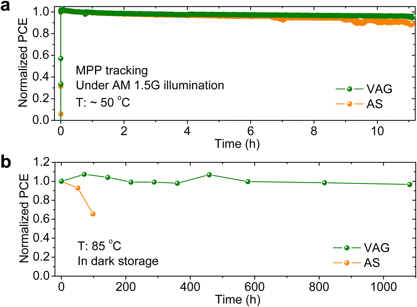 | ||
| Fig. 5 Durability of perovskite–perovskite–Si MTJSCs. Evolution of normalized PCEs of perovskite–perovskite–Si MTJSCs (a) under continuous AM 1.5G illumination at ∼50 °C for MPP tracking and (b) in dark storage at 85 °C. All devices without encapsulation were tested in an N2-filled glovebox. | ||
Conclusions
Using experimental optimizations and optical simulations, we successfully demonstrate high-efficiency perovskite–perovskite–Si MTJSCs, achieving a record PCE of 24.4%. A high overall JSC is realized up to 11.6 mA cm−2 by optimized light management and good current matching for both perovskite sub-cells. Using an AS-free VAG process enables a high-quality FAPbI3 middle perovskite sub-cell (free of wrinkles, cracks, and pinholes), resulting in low non-radiative recombination loss at the perovskite/ETL interfaces. This improves VOC up to 2.84 V in a triple-junction architecture. Non-encapsulated MTJSCs retain 96.6% of initial PCE in dark storage aging at 85 °C for 1081 h. Our work offers advanced approaches for the fabrication of efficient perovskite-based triple-junction PVs.Experimental procedures
Materials
Lead iodide (PbI2, TCI, 99.99%), lead bromide (PbBr2, TCI), formamidinium iodide (FAI, GreatCell Solar), formamidinium bromide (FAI, GreatCell Solar), methylammonium chloride (MACl, Dyenamo), cesium iodide (CsI, Alfa Aesar), cesium bromide (CsBr, Alfa Aesar), [2-(9H-carbazol-9-yl)ethyl] phosphonic acid (2PACz, TCI), fullerene (C60, Sigma Aldrich, 99.5%), 2,9-dimethyl-4,7-diphenyl-1,10-phenanthroline (BCP, Lumescence Technology), lithium fluoride (LiF, Luminescence Technology), magnesium fluoride (MgF2, Sigma Aldrich), dimethylformamide (DMF, Sigma Aldrich, anhydrous, 99.8%), dimethyl sulfoxide (DMSO, Sigma Aldrich, anhydrous, ≥99.9%), ethyl ethanoate (EA, Sigma Aldrich, anhydrous, 99.8%), ethanol (VWR Chemicals, absolute, 99.8%), tetrakis(dimethylamino)tin(IV) (TDMASn, 99.99%-Sn, Strem Chemicals), indium tin oxide (ITO) or indium zinc oxide (IZO), hydrogen-doped indium oxide (IOH) (using InO/ZnO target, Kurt J. Lesker Company, 90/10 wt%, 99.99%), nickel oxide (NiOx) (using NiOx target, Kurt J. Lesker Company, 99.995%).Preparation of middle perovskite (∼1.52 eV) precursor
An optimum 1.3 M FAPbI3 perovskite precursor was prepared in a N2-filled glovebox (O2 < 0.5 ppm and H2O < 0.4 ppm) from 1.43 M PbI2, 1.3 M FAI, and 30 mol% MACl dissolved in a mixed solvent of DMF and DMSO with a volume ratio of 4![[thin space (1/6-em)]](https://www.rsc.org/images/entities/char_2009.gif) :1. The thickness of MBG perovskite layer was optimized by varying the concentration of perovskite precursor from 1.1 to 1.9 M.
:1. The thickness of MBG perovskite layer was optimized by varying the concentration of perovskite precursor from 1.1 to 1.9 M.
Preparation of top perovskite (∼1.84 eV) precursor
An optimum 0.8 M FA0.8Cs0.2Pb(I0.5Br0.5)3 perovskite precursor was prepared in a glovebox from 0.4 M PbI2, 0.4 M PbBr2, 0.32 M FAI, 0.32 M FAI, 0.08 M CsI, and 0.08 M CsBr dissolved in a mixed solvent of DMF and DMSO with a volume ratio of 4:1. The thickness of WBG perovskite layer was optimized by varying the concentration of perovskite precursor from 0.6 to 1.0 M.
Deposition of middle perovskite (∼1.52 eV) thin film
FAPbI3 perovskite thin film was fabricated using either anti-solvent (AS) quenching or vacuum-assisted growth (VAG) methods.6,7 For the AS process, the FAPbI3 solution was deposited by spin-coating at 1000 rpm for 10 s and 5000 rpm for 40 s. 150 μL EA was dropped at 30 s during the second step of spin coating. For the VAG process, the FAPbI3 solution was deposited by spin-coating at 5000 rpm for 30 s, and the thin film was promptly transferred into a vacuum chamber with an optimized vacuum time of 30 s. Wet FAPbI3 thin films fabricated from both methods were then annealed at 120 °C for 20 min.Deposition of top perovskite (∼1.84 eV) thin film
FA0.8Cs0.2Pb(I0.5Br0.5)3 perovskite thin film was deposited by spin-coating at 1000 rpm for 10 s and 5000 rpm for 30 s. 150 μL EA was dropped at 11 s during the second step of spin coating. The wet FA0.8Cs0.2Pb(I0.5Br0.5)3 thin film was then annealed at 150 °C for 20 min.Atomic layer deposition of tin oxide (SnOx) layer
A 35-nm SnOx thin film was fabricated by atomic layer deposition (ALD) with 300 cycles in an ALD system (Picosun, R200 Advanced) at 90 °C using the precursors of TDMASn (pulse time 1.6s, purge time 12s) and water (pulse time 0.1s, purge time 16s), as reported in our previous work.7 High-purity argon (Ar, 99.999%) was used as carrier gas and purge gas. The line flows of TDMASn and water were set to 120 and 150 standard cubic centimeters per minute (sccm), respectively. The TDMASn source container was preheated for 1hour at 70 °C to ensure thermal equilibrium.
Fabrication of single-junction perovskite (∼1.52 eV or ∼1.84 eV) solar cells
The single-junction perovskite solar cells (middle or top sub-cell) were fabricated in a p–i–n architecture of ITO/2PACz/perovskite/(LiF)/C60/BCP/gold (Au). ITO substrates (sheet resistance 15 Ω sq−1, Luminescence Technology) were cleaned with acetone and isopropanol in an ultrasonic bath for 10 min, respectively. Substrates were further treated with an oxygen plasma for 3 min. A ∼0.475 mg mL−1 2PACz (in anhydrous ethanol) solution was spin-coated on the ITO substrates at 3000 rpm for 30 s and subsequently annealed at 100 °C for 10 min. FAPbI3 perovskite thin films were fabricated using VAG and AS methods. FA0.8Cs0.2Pb(I0.5Br0.5)3 perovskite thin film was fabricated with AS method, and a 1-nm LiF thin layer was subsequently thermally evaporated on top. Finally, 30-nm C60, 5-nm BCP, and 75-nm Au were thermally evaporated to complete the devices. The active area of single-junction devices was 0.105 cm2.Fabrication of silicon bottom cells
The silicon (Si) bottom cells were fabricated from polished n-type Float Zone (FZ) wafers (∼2 Ω cm) with a thickness of ∼200 μm after potassium hydroxide (KOH) etching before the fabrication process. A thick silicon dioxide (SiOx) was grown to isolate the rear minority carrier hole contact from the defective cleaved edge of the finished cell. The cell's active area was defined by ablating the SiOx locally from the rear side and KOH etching to remove any laser damage. The SiOx from the front side was removed by a single-side treatment with hydrofluoric (HF) acid. We grew a thin SiOx and deposited amorphous Si (a-Si) on top of the SiOx. We doped the a-Si layer by implanting pH and Boron to the front and rear sides, respectively, and formed the electron- and hole-selective passivating polysilicon-on-passivating-oxide (n-POLO and p-POLO) contacts by furnace annealing and oxidation. The grown SiOx on the rear side was patterned by laser ablation such that only islands of p-POLO contacts remained at the rear side after KOH etching and texturization. The SiOx protecting the front n-POLO contact was removed by single-side HF treatment, and the front contact's poly-Si was thinned to ∼50 nm in an ammonium–peroxide mixture. The rear side was passivated by a stack of aluminum oxide (Al2O3), silicon nitride (SiNy), and SiOx, and the front side received an Al2O3 layer for hydrogenation of the n-POLO front contact. The dielectric layer stack on the rear side was ablated locally on the p-POLO islands to provide electrical contact to the metal. Next, the cell precursor was dipped in diluted HF to remove the Al2O3 hydrogenation source from the front side, and 20 nm ITO was sputtered on the front n-POLO contact. Finally, the aluminum (Al) back contact was evaporated on the rear side, and 16 × 16 mm2 substrates with 1 cm2 cells were cleaved from the wafer.Fabrication of perovskite–perovskite–Si monolithic triple-junction solar cells
The architecture of monolithic triple-junction solar cells (MTJSCs) is Si/ITO/NiOx/2PACz/FAPbI3/C60/SnOx/ITO/NiOx/2PACz/Cs0.2FA0.8Pb(I0.5Br0.5)3/LiF/C60/SnOx/IZO/Au/MgF2. Si substrates with ∼20 nm ITO layer on the front side were cleaned with isopropanol by spin-coating. A ∼15-nm NiOx layer was sputtered on top of Si/ITO substrates. 2PACz, FAPbI3, Cs0.2FA0.8Pb(I0.5Br0.5)3, and LiF thin films were fabricated in the same condition as with the single-junction device. C60 thin films were thermally evaporated with thicknesses of ∼15 nm. A 35-nm SnOx layer was fabricated by ALD. The middle ITO recombination layer (∼15 nm) and top IZO electrode were fabricated by a sputtering system. A ∼300-nm Au was then thermally evaporated with a c-shaped mask (framing an active area of 52.25 mm2). Finally, a ∼125-nm MgF2 antireflection coating was thermally evaporated to complete the triple junction.Current-density–voltage (J–V) and maximum power point (MPP) tracking measurements
The J–V characteristics of the devices were measured using a class AAA 21-channel LED solar simulator (Wavelabs Solar Metrology Systems Sinus-70) equipped with a source meter (Keithley 2400) with an air-mass AM 1.5G spectrum (100 mW cm−2 illumination). The scan rate was set to 0.6 V s−1, and a certified Si reference solar cell (KG0, Newport) was used for calibration of the illumination intensity of the solar simulator. The stabilized power conversion efficiency (SPCE) was determined by maximum power point (MPP) tracking under continuous AM 1.5G illumination. The temperature of the devices was not controlled during J–V measurements. Devices were placed on a hotplate at 85 °C in the dark for thermal stability testing.External quantum efficiency (EQE) measurements
EQE spectra for triple-junction solar cells were measured using a Bentham PVE300 system with a modulated monochromatic light. A chopping frequency was set to ∼580 Hz, and an integration time was set to 500 ms. The EQE response was calibrated using Si and germanium (Ge) certified reference cells for 300–1100 nm and 1000–1300 nm wavelength regions, respectively. For the EQE measurements of each sub-cell, we used a combination of different filters and bias light sources to saturate the other two sub-cells. For the top cell, the light-emitting diode (LED) lights (780 nm and 940 nm) and a long-pass filter (with cut-on wavelength at 850nm, FGL850M) were used. For the middle cell, the LED lights (465 nm and 940 nm) and a long-pass filter (FGL850M) were used. For the bottom cell, the LED lights (465 nm and 780 nm) and a bandpass filter (335–610nm, FGB37M) were used.
Scanning electron microscopy (SEM)
Top-view and cross-sectional SEM images of the perovskite thin films and triple-junction solar cells were taken using a Zeiss Supra60 VP SEM system.Atomic force microscopy (AFM)
Surface topographies of perovskite thin films were inspected using Nano Wizard II (JPK Instruments). The scanning area was 10 μm × 10 μm.Optical microscopy
Optical microscopy images of perovskite thin films were collected using ZEISS Axioplan 2 microscope.X-ray diffraction (XRD)
XRD was performed on the layer stack of ITO/2PACz/FAPbI3 using a Bruker D2Phaser system with Cu-Kα radiation (λ = 1.5405 Å) in Bragg–Brentano configuration using a LynxEye detector.Time-resolved photoluminescence (TRPL)
TRPL was performed in ambient air based on an FLSP920 Fluorescence Spectrometer (Edinburgh Instruments Ltd.) using the TCSPC acquisition technique. A picosecond pulsed laser diode (PicoQuant, 635 nm) externally triggered by a delay generator (repetition rate: 500 kHz) was used as the excitation light. The emission was collected by a photomultiplier tube (Hamamatsu R928P).Photoluminescence quantum yield (PLQY)
PLQY measurements were conducted inside an integrating sphere (LabSphere, 15 cm diameter) in ambient air. A green laser (Coherent or LD-515-10MG from Roithner Lasertechnik) was directed into the sphere via a small entrance port. An optical fiber was used to collect the emission from the exit port of the sphere and guide it to the spectrometers (QE65 Pro from Ocean Optics and AvaSpec-ULS2048x64TEC from Avantes). Spectral response was calibrated using a calibration lamp (HL-3plus-INT-Cal from Ocean Optics). Raw measured spectra were recalculated to give power spectra using the integration time. The samples were placed at an angle of 15° with respect to the laser beam to avoid specular reflectance toward the entrance port. The ‘implied VOC’ was derived via:46,47,60
V
OC-rad be estimated by the following equation:61
Mott–Schottky (MS) measurements
MS measurements for single-junction solar cells were performed using a PAIOS system (Fluxim AG) in the dark with a constant frequency of 30 kHz and an amplitude of 20 mV.Dark J–V curves and ideality factor measurements
Dark J–V curves and ideality factor measurements were performed using a PAIOS system with a white light emitting diode (Cree XP-G). VOC can be estimated by the following equation:6,62where kB is the Boltzmann constant, T is the absolute temperature, q is the elementary charge, Jt is the theory of current density, and J0 is the reverse saturation current density.
The ideality factor was studied by measuring light intensity-dependent VOC. Logarithmic VOC can be linear fitted by the equation:6,63
Space-charge-limited current (SCLC) measurements
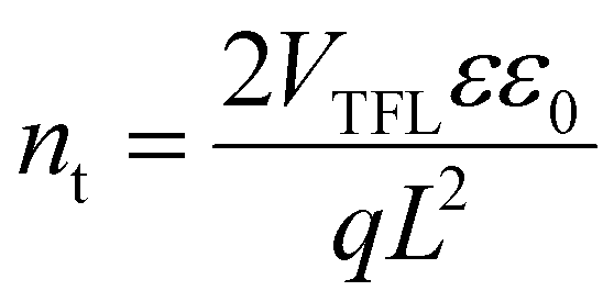
SCLC measurements were conducted on the electron-only single-junction semitransparent devices in the architecture of ITO/SnO2/FAPbI3/C60/SnOx/IZO/Au. Dark current-density–voltage (J–V) characteristics were performed using a PAIOS system in the dark at the range of 0–2 V with a settling time of 40 ms. The trap density (nt) can be expressed in the following equation:6,28,53–55,64where VTFL is the trap-filling limit voltage, L is the thickness of the perovskite thin film, ε is the relative dielectric constant of perovskite, ε0 is the vacuum permittivity, and q is the elementary charge.
Electrical impedance spectroscopy (EIS)
EIS was performed using PAIOS system equipped with a white light emitting diode (Cree XP-G) under a bias of 1 V and an amplitude of 30 mV. Nyquist plots were fitted by the Z-View program.Transient photovoltage (TPV) measurements
TPV measurements were conducted using a PAIOS system. A high resistor (1 MΩ) is used to form an open-circuit condition, so that the current is zero during the whole measurement. A small perturbation light pulse to the background illumination is applied to a constant offset light intensity.Electroluminescence (EL) and photoluminescence (PL) imaging
The EL and PL images were acquired with a 2.1 megapixel scientific CMOS camera (Quantalux sCMOS camera, Thorlabs). The EL and PL were filtered with a 775nm shortpass (Edmund Optics) stacked on top of a 665nm longpass (Thorlabs) to remove the excitation light during PL imaging. Two blue LED bars (CCS Inc.) were used an excitation source for PL imaging. The perovskite thin films or solar cells were biased using a Keithley 2450 SMU, as it was reported in our previous work.7 All measurements were performed in ambient air.
Simulations
Simulations were performed using the open-source modelling platform EYcalc.65 Details of this modeling platform have been published in our previous work.5,34,35 The optical simulations apply state-of-the-art optical data and electrical parameters that were derived from optical and electrical characterization of our single-junction devices.35 The thickness of each layer was chosen as follow: MgF2 (125 nm)/IZO (90 nm)/SnOx (20 nm)/C60 (15 nm)/top perovskite (varied)/2PACz-NiOx (5 nm)/ITO (15 nm)/SnOx (20 nm)/C60 (15 nm)/middle perovskite (varied)/2PACz-NiOx (15 nm)/ITO (5 nm)/a-Si(n) (40 nm)/a-Si(i) (10 nm)/c-Si (250 μm)/a-Si(i) (10 nm)/a-Si(p) (10 nm)/ITO (80 nm)/Ag (250 nm). The champion perovskite–perovskite–Si monolithic triple-junction solar cell was chosen using a 1.84 eV top perovskite with a thickness of 200 nm and 1.52 eV middle perovskite with a thickness of 1000 nm. The best simulated power conversion efficiency is 24.8% with an open-circuit voltage of 2.95 V and a FF of 0.717.In this study, we use our in-house developed EY modelling platform EYCalc available as an open-source software project.35 A comprehensive description of the software is provided by Schmager et al.35 Here, we provide a brief overview of its structure and working principles. This platform consists of four modules: irradiance, optics, electrics, and EY module. Based on data from the typical meteorological year (TMY3)66 for various locations in the USA, the irradiance module computes direct and diffuse irradiance spectra for each hour of the year. Then we extract the appropriate hourly-resolved irradiance from the TMY3 data using a cloud model and the simplified model of atmospheric radiative transfer of sunshine (SMARTS).67 In analyses conducted under standard test conditions, the platform foregoes the utilization of location-specific irradiance spectra, opting instead to employ solely the AM 1.5G spectrum. Afterward, the optics module calculates spectrally and angularly resolved optical properties, including absorptance, reflectance, and transmittance for the provided layer stack. The optics module computes the optical parameters by combining a series expansion of Beer–Lambert law or the transfer matrix method (TMM), depending on whether the layer is optically coherent (thin) or optically incoherent (thick), respectively. The platform is able to handle textured interfaces using geometrical ray tracing.68
Next, we calculate the hourly resolved photogenerated current density (JG) in the absorber layers by the EY module by merging the output from the irradiance and optics modules while considering the solar cell's rotation and tilt. Then, we determine the photovoltaic parameters in the electrical module. The electrical module subsequently calculates temperature-dependent J–V characteristics and MPP for each hourly resolved JG. For this process, an analytical one-diode or two-diode model or a precise numerical method can be used. In this study, we used the second method by implementing a two-diode model in LTspice.69 The EY module then calculates the annual EY by considering each hour's contributions throughout the year for different climatic locations. In case of STC analysis, the PCE of the solar cell is computed based on the values obtained in the previous steps. Temperature effects are taken into account using temperature coefficients for the VOC and JG. The cell temperature is estimated using the Nominal Operating Cell Temperature (NOCT) model, assuming NOCT = 48° and extracting the insolation on the cell and ambient air temperature from TMY3 data.
Author contributions
H. H., B. A. N., and U. W. P. convinced the idea for this project. H. H. did the fabrication of triple-junction solar cells and the rest of characterizations. S. X. A., S. O., and F. G. contributed to the simulation of triple-junction solar cells. Y. L. conducted TRPL and PLQY measurements. R. S. conducted XRD. F. S. and F. L. conducted the EL imaging. Q. J. performed AFM. H. H. and T. F. fabricated ALD-SnOx layers. B. A. N. and A. D. performed SEM. H. H. and T. P. optimized 2PACz layer. S. M. optimized sputtering TCO. M. R. and R. P. provided the Si bottom cells and contributed with their expertise on Si solar cells. B. A. N. and U. W. P. supervised the project. H. H. wrote the original draft. B. A. N. and U. W. P. reviewed and edited the manuscript. All authors contributed to the discussions and the final reviewing of the manuscript.Conflicts of interest
There are no conflicts to declare.Acknowledgements
The authors acknowledge R. Winter (ISFH), and G. Glowatzki (MBE of Leibniz Universität Hannover) for fabricating the bottom Si cells. The Karlsruhe Nano Micro Facility (KNMF) at KIT is acknowledged for employing the ALD system. Financial support by the Initiating and Networking funding of the Helmholtz Association (Project Zeitenwende and the Solar Technology Acceleration Platform (Solar TAP)), the program oriented funding IV of the Helmholtz Association (Materials and Technologies for the Energy Transition, Topic 1: Photovoltaics and Wind Energy, Code: 38.01.03), the German Federal Ministry for Economic Affairs and Climate Action (BMWK) through the project 27Plus6 (03EE1056B), and the Karlsruhe School of Optics and Photonics (KSOP) is gratefully acknowledged. H. H. and T. P. are grateful to thank financial support from the Chinese Scholarship Council (CSC). B. A. N. acknowledges the financial support from the European Union's Horizon 2020 research and innovation program under the Marie Skłodowska-Curie (grant agreement no. 840937). The study is co-funded by the European Union (ERC, Lami-Pero,101087673). Views and opinions expressed are however those of the author(s) only and do not necessarily reflect those of the European Union or the European Research Council. Neither the European Union nor the granting authority can be held responsible for them.References
- M. A. Green, E. D. Dunlop, G. Siefer, M. Yoshita, N. Kopidakis, K. Bothe and X. Hao, Prog. Photovoltaics Res. Appl., 2023, 31, 3–16 CrossRef.
- Y. Hou, E. Aydin, M. De Bastiani, C. Xiao, F. H. Isikgor, D. J. Xue, B. Chen, H. Chen, B. Bahrami, A. H. Chowdhury, A. Johnston, S. W. Baek, Z. Huang, M. Wei, Y. Dong, J. Troughton, R. Jalmood, A. J. Mirabelli, T. G. Allen, E. Van Kerschaver, M. I. Saidaminov, D. Baran, Q. Qiao, K. Zhu, S. De Wolf and E. H. Sargent, Science, 2020, 367, 1135–1140 CrossRef CAS PubMed.
- A. Al-Ashouri, E. Köhnen, B. Li, A. Magomedov, H. Hempel, P. Caprioglio, J. A. Márquez, A. B. M. Vilches, E. Kasparavicius, J. A. Smith, N. Phung, D. Menzel, M. Grischek, L. Kegelmann, D. Skroblin, C. Gollwitzer, T. Malinauskas, M. Jošt, G. Matič, B. Rech, R. Schlatmann, M. Topič, L. Korte, A. Abate, B. Stannowski, D. Neher, M. Stolterfoht, T. Unold, V. Getautis and S. Albrecht, Science, 2020, 370, 1300–1309 CrossRef CAS PubMed.
- P. Tockhorn, J. Sutter, A. Cruz, P. Wagner, K. Jäger, D. Yoo, F. Lang, M. Grischek, B. Li, J. Li, O. Shargaieva, E. Unger, A. Al-Ashouri, E. Köhnen, M. Stolterfoht, D. Neher, R. Schlatmann, B. Rech, B. Stannowski, S. Albrecht and C. Becker, Nat. Nanotechnol., 2022, 17, 1214–1221 CrossRef CAS PubMed.
- M. A. Ruiz-Preciado, F. Gota, P. Fassl, I. M. Hossain, R. Singh, F. Laufer, F. Schackmar, T. Feeney, A. Farag, I. Allegro, H. Hu, S. Gharibzadeh, B. A. Nejand, V. S. Gevaerts, M. Simor, P. J. Bolt and U. W. Paetzold, ACS Energy Lett., 2022, 7, 2273–2281 CrossRef CAS PubMed.
- H. Hu, S. Moghadamzadeh, R. Azmi, Y. Li, M. Kaiser, J. C. Fischer, Q. Jin, J. Maibach, I. M. Hossain, U. W. Paetzold and B. Abdollahi Nejand, Adv. Funct. Mater., 2022, 32, 2107650 CrossRef CAS.
- B. Abdollahi Nejand, D. B. Ritzer, H. Hu, F. Schackmar, S. Moghadamzadeh, T. Feeney, R. Singh, F. Laufer, R. Schmager, R. Azmi, M. Kaiser, T. Abzieher, S. Gharibzadeh, E. Ahlswede, U. Lemmer, B. S. Richards and U. W. Paetzold, Nat. Energy, 2022, 7, 620–630 CrossRef CAS.
- R. Lin, J. Xu, M. Wei, Y. Wang, Z. Qin, Z. Liu, J. Wu, K. Xiao, B. Chen, S. M. Park, G. Chen, H. R. Atapattu, K. R. Graham, J. Xu, J. Zhu, L. Li, C. Zhang, E. H. Sargent and H. Tan, Nature, 2022, 603, 73–78 CrossRef CAS PubMed.
- S. P. Bremner, C. Yi, I. Almansouri, A. Ho-Baillie and M. A. Green, Sol. Energy, 2016, 135, 750–757 CrossRef CAS.
- NREL National Center for Photovoltaics, Best research-cell efficiency chart, October 2023, https://www.nrel.gov/pv/cellefficiency.html.
- M. T. Hörantner, T. Leijtens, M. E. Ziffer, G. E. Eperon, M. G. Christoforo, M. D. McGehee and H. J. Snaith, ACS Energy Lett., 2017, 2, 2506–2513 CrossRef.
- J. Werner, F. Sahli, F. Fu, J. J. Diaz Leon, A. Walter, B. A. Kamino, B. Niesen, S. Nicolay, Q. Jeangros and C. Ballif, ACS Energy Lett., 2018, 3, 2052–2058 CrossRef CAS.
- M. Haider and J. L. Yang, Rare Met., 2020, 39, 745–747 CrossRef CAS.
- D. P. McMeekin, S. Mahesh, N. K. Noel, M. T. Klug, J. C. Lim, J. H. Warby, J. M. Ball, L. M. Herz, M. B. Johnston and H. J. Snaith, Joule, 2019, 3, 387–401 CrossRef CAS.
- J. Zheng, G. Wang, W. Duan, M. A. Mahmud, H. Yi, C. Xu, A. Lambertz, S. Bremner, K. Ding, S. Huang and A. W. Y. Ho-Baillie, ACS Energy Lett., 2022, 7, 3003–3005 CrossRef CAS.
- J. Wang, V. Zardetto, K. Datta, D. Zhang, M. M. Wienk and R. A. J. Janssen, Nat. Commun., 2020, 11, 1–10 CrossRef PubMed.
- K. Xiao, J. Wen, Q. Han, R. Lin, Y. Gao, S. Gu, Y. Zang, Y. Nie, J. Zhu, J. Xu and H. Tan, ACS Energy Lett., 2020, 5, 2819–2826 CrossRef CAS.
- Z. Wang, L. Zeng, T. Zhu, H. Chen, B. Chen, D. J. Kubicki, A. Balvanz, C. Li, A. Maxwell, E. Ugur, R. dos Reis, M. Cheng, G. Yang, B. Subedi, D. Luo, J. Hu, J. Wang, S. Teale, S. Mahesh, S. Wang, S. Hu, E. D. Jung, M. Wei, S. M. Park, L. Grater, E. Aydin, Z. Song, N. J. Podraza, Z. H. Lu, J. Huang, V. P. Dravid, S. De Wolf, Y. Yan, M. Grätzel, M. G. Kanatzidis and E. H. Sargent, Nature, 2023, 618, 74–79 CrossRef CAS PubMed.
- J. Wang, L. Zeng, D. Zhang, A. Maxwell, H. Chen, K. Datta, A. Caiazzo, W. H. M. Remmerswaal, N. R. M. Schipper, Z. Chen, K. Ho, A. Dasgupta, G. Kusch, R. Ollearo, L. Bellini, S. Hu, Z. Wang, C. Li, S. Teale, L. Grater, B. Chen, M. M. Wienk, R. A. Oliver, H. J. Snaith, R. A. J. Janssen and E. H. Sargent, Nat. Energy, 2024, 9, 70–80 CrossRef CAS.
- Y. J. Choi, S. Y. Lim, J. H. Park, S. G. Ji and J. Y. Kim, ACS Energy Lett., 2023, 8, 3141–3146 CrossRef CAS.
- M. Heydarian, M. Heydarian, A. J. Bett, M. Bivour, F. Schindler, M. Hermle, M. C. Schubert, P. S. C. Schulze, J. Borchert and S. W. Glunz, ACS Energy Lett., 2023, 8, 4186–4192 CrossRef CAS PubMed.
- S. H. Turren-Cruz, A. Hagfeldt and M. Saliba, Science, 2018, 362, 449–453 CrossRef CAS PubMed.
- M. Kim, G. H. Kim, T. K. Lee, I. W. Choi, H. W. Choi, Y. Jo, Y. J. Yoon, J. W. Kim, J. Lee, D. Huh, H. Lee, S. K. Kwak, J. Y. Kim and D. S. Kim, Joule, 2019, 3, 2179–2192 CrossRef CAS.
- M. Jeong, I. W. Choi, E. M. Go, Y. Cho, M. Kim, B. Lee, S. Jeong, Y. Jo, H. W. Choi, J. Lee, J. H. Bae, S. K. Kwak, D. S. Kim and C. Yang, Science, 2020, 369, 1615–1620 CrossRef CAS PubMed.
- H. Lu, Y. Liu, P. Ahlawat, A. Mishra, W. R. Tress, F. T. Eickemeyer, Y. Yang, F. Fu, Z. Wang, C. E. Avalos, B. I. Carlsen, A. Agarwalla, X. Zhang, X. Li, Y. Zhan, S. M. Zakeeruddin, L. Emsley, U. Rothlisberger, L. Zheng, A. Hagfeldt and M. Grätzel, Science, 2020, 370, eabb8985 CrossRef CAS PubMed.
- G. Kim, H. Min, K. S. Lee, D. Y. Lee, S. M. Yoon and S. Il Seok, Science, 2020, 370, 108–112 CrossRef CAS PubMed.
- W. Hui, L. Chao, H. Lu, F. Xia, Q. Wei, Z. Su, T. Niu, L. Tao, B. Du, D. Li, Y. Wang, H. Dong, S. Zuo, B. Li, W. Shi, X. Ran, P. Li, H. Zhang, Z. Wu, C. Ran, L. Song, G. Xing, X. Gao, J. Zhang, Y. Xia, Y. Chen and W. Huang, Science, 2021, 371, 1359–1364 CrossRef CAS PubMed.
- H. Min, M. Kim, S. U. Lee, H. Kim, G. Kim, K. Choi, J. H. Lee and S. Il Seok, Science, 2019, 366, 749–753 CrossRef CAS PubMed.
- S. G. Kim, J. H. Kim, P. Ramming, Y. Zhong, K. Schötz, S. J. Kwon, S. Huettner, F. Panzer and N. G. Park, Nat. Commun., 2021, 12, 1–10 CrossRef PubMed.
- K. A. Bush, N. Rolston, A. Gold-Parker, S. Manzoor, J. Hausele, Z. J. Yu, J. A. Raiford, R. Cheacharoen, Z. C. Holman, M. F. Toney, R. H. Dauskardt and M. D. McGehee, ACS Energy Lett., 2018, 3, 1225–1232 CrossRef CAS.
- S. Braunger, L. E. Mundt, C. M. Wolff, M. Mews, C. Rehermann, M. Jošt, A. Tejada, D. Eisenhauer, C. Becker, J. A. Guerra, E. Unger, L. Korte, D. Neher, M. C. Schubert, B. Rech and S. Albrecht, J. Phys. Chem. C, 2018, 122, 17123–17135 CrossRef CAS.
- P. Hang, C. Kan, B. Li, Y. Yao, Z. Hu, Y. Zhang, J. Xie, Y. Wang, D. Yang and X. Yu, Adv. Funct. Mater., 2023, 33, 2214381 CrossRef CAS.
- A. Farag, P. Fassl, H. Hu, T. Feeney, A. Quintilla, M. A. Ruiz-Preciado, W. Hempel, D. Bagrowski, P. Noack, B. Wattenberg, T. Dippell and U. W. Paetzold, Adv. Funct. Mater., 2023, 33, 2210758 CrossRef CAS.
- F. Gota, S. X. An, H. Hu, B. Abdollahi Nejand and U. W. Paetzold, Adv. Opt. Mater., 2023, 11, 2201691 CrossRef CAS.
- R. Schmager, M. Langenhorst, J. Lehr, U. Lemmer, B. S. Richards and U. W. Paetzold, Opt. Express, 2019, 27, A507 CrossRef CAS PubMed.
- H. Hu, D. B. Ritzer, A. Diercks, Y. Li, R. Singh, P. Fassl, Q. Jin, F. Schackmar, U. W. Paetzold and B. Abdollahi Nejand, Joule, 2023, 7, 1574–1592 CrossRef CAS.
- J. Chen, L. Zuo, Y. Zhang, X. Lian, W. Fu, J. Yan, J. Li, G. Wu, C. Z. Li and H. Chen, Adv. Energy Mater., 2018, 8, 1800438 CrossRef.
- Y. Zhou, M. Yang, O. S. Game, W. Wu, J. Kwun, M. A. Strauss, Y. Yan, J. Huang, K. Zhu and N. P. Padture, ACS Appl. Mater. Interfaces, 2016, 8, 2232–2237 CrossRef CAS PubMed.
- J. Ma, M. Qin, Y. Li, X. Wu, Z. Qin, Y. Wu, G. Fang and X. Lu, Matter, 2021, 4, 313–327 CrossRef CAS.
- K. Liu, Z. Wang, S. Qu and L. Ding, Nano-Micro Lett., 2023, 15, 1–5 Search PubMed.
- X. Li, D. Bi, C. Yi, J. D. Décoppet, J. Luo, S. M. Zakeeruddin, A. Hagfeldt and M. Grätzel, Science, 2016, 353, 58–62 CrossRef CAS PubMed.
- W. Xiang, J. Zhang, S. (Frank) Liu, S. Albrecht, A. Hagfeldt and Z. Wang, Joule, 2022, 6, 315–339 CrossRef CAS.
- T. Du, T. J. Macdonald, R. X. Yang, M. Li, Z. Jiang, L. Mohan, W. Xu, Z. Su, X. Gao, R. Whiteley, C. T. Lin, G. Min, S. A. Haque, J. R. Durrant, K. A. Persson, M. A. McLachlan and J. Briscoe, Adv. Mater., 2022, 34, 1–10 Search PubMed.
- B. Yang, D. Bogachuk, J. Suo, L. Wagner, H. Kim, J. Lim, A. Hinsch, G. Boschloo, M. K. Nazeeruddin and A. Hagfeldt, Chem. Soc. Rev., 2022, 51, 7509–7530 RSC.
- X. Jiang, X. Wang, X. Wu, S. Zhang, B. Liu, D. Zhang, B. Li, P. Xiao, F. Xu, H. Lu, T. Chen, A. K. Y. Jen, S. Yang and Z. Zhu, Adv. Energy Mater., 2023, 13, 1–8 Search PubMed.
- D. Zhang, H. Zhang, H. Guo, F. Ye, S. Liu and Y. Wu, Adv. Funct. Mater., 2022, 2200174, 1–9 Search PubMed.
- S. Gharibzadeh, P. Fassl, I. M. Hossain, P. Rohrbeck, M. Frericks, M. Schmidt, T. Duong, M. R. Khan, T. Abzieher, B. A. Nejand, F. Schackmar, O. Almora, T. Feeney, R. Singh, D. Fuchs, U. Lemmer, J. P. Hofmann, S. A. L. Weber and U. W. Paetzold, Energy Environ. Sci., 2021, 14, 5875–5893 RSC.
- B. Abdollahi Nejand, I. M. Hossain, M. Jakoby, S. Moghadamzadeh, T. Abzieher, S. Gharibzadeh, J. A. Schwenzer, P. Nazari, F. Schackmar, D. Hauschild, L. Weinhardt, U. Lemmer, B. S. Richards, I. A. Howard and U. W. Paetzold, Adv. Energy Mater., 2020, 10, 1902583 CrossRef CAS.
- Z. Dai, S. K. Yadavalli, M. Chen, A. Abbaspourtamijani, Y. Qi and N. P. Padture, Science, 2021, 372, 618–622 CrossRef CAS PubMed.
- J. Liu, M. De Bastiani, E. Aydin, G. T. Harrison, Y. Gao, R. R. Pradhan, M. K. Eswaran, M. Mandal, W. Yan, A. Seitkhan, M. Babics, A. S. Subbiah, E. Ugur, F. Xu, L. Xu, M. Wang, A. ur Rehman, A. Razzaq, J. Kang, R. Azmi, A. A. Said, F. H. Isikgor, T. G. Allen, D. Andrienko, U. Schwingenschlögl, F. Laquai and S. De Wolf, Science, 2022, 377, 302–306 CrossRef CAS PubMed.
- J. Chung, S. W. Kim, Y. Li, T. Mariam, X. Wang, M. Rajakaruna, M. M. Saeed, A. Abudulimu, S. S. Shin, K. N. Guye, Z. Huang, R. J. E. Westbrook, E. Miller, B. Subedi, N. J. Podraza, M. J. Heben, R. J. Ellingson, D. S. Ginger, Z. Song and Y. Yan, Adv. Energy Mater., 2023, 2300595, 1–10 Search PubMed.
- A. Gerber, V. Huhn, T. M. H. Tran, M. Siegloch, Y. Augarten, B. E. Pieters and U. Rau, Sol. Energy Mater. Sol. Cells, 2015, 135, 35–42 CrossRef CAS.
- D. Shi, V. Adinolfi, R. Comin, M. Yuan, E. Alarousu, A. Buin, Y. Chen, S. Hoogland, A. Rothenberger, K. Katsiev, Y. Losovyj, X. Zhang, P. A. Dowben, O. F. Mohammed, E. H. Sargent and O. M. Bakr, Science, 2015, 347, 519–522 CrossRef CAS PubMed.
- S. Akin, E. Akman and S. Sonmezoglu, Adv. Funct. Mater., 2020, 30, 2002964 CrossRef CAS.
- Q. Han, S. H. Bae, P. Sun, Y. T. Hsieh, Y. Yang, Y. S. Rim, H. Zhao, Q. Chen, W. Shi, G. Li and Y. Yeng, Adv. Mater., 2016, 28, 2253–2258 CrossRef CAS PubMed.
- R. Chen, S. Liu, X. Xu, F. Ren, J. Zhou, X. Tian, Z. Yang, X. Guanz, Z. Liu, S. Zhang, Y. Zhang, Y. Wu, L. Han, Y. Qi and W. Chen, Energy Environ. Sci., 2022, 5–8 CAS.
- X. Zheng, B. Chen, J. Dai, Y. Fang, Y. Bai, Y. Lin, H. Wei, X. C. Zeng and J. Huang, Nat. Energy, 2017, 2, 1–9 Search PubMed.
- J. Xu, C. C. Boyd, Z. J. Yu, A. F. Palmstrom, D. J. Witter, B. W. Larson, R. M. France, J. Werner, S. P. Harvey, E. J. Wolf, W. Weigand, S. Manzoor, M. F. A. M. Van Hest, J. J. Berry, J. M. Luther, Z. C. Holman and M. D. McGehee, Science, 2020, 367, 1097–1104 CrossRef CAS PubMed.
- W. Liu, H. Raza, X. Hu, S. Liu and Z. Liu, Mater. Futures, 2023, 2, 012103 CrossRef.
- M. Stolterfoht, M. Grischek, P. Caprioglio, C. M. Wolff, E. Gutierrez-Partida, F. Peña-Camargo, D. Rothhardt, S. Zhang, M. Raoufi, J. Wolansky, M. Abdi-Jalebi, S. D. Stranks, S. Albrecht, T. Kirchartz and D. Neher, Adv. Mater., 2020, 32, 2000080 CrossRef CAS PubMed.
- L. Krückemeier, U. Rau, M. Stolterfoht and T. Kirchartz, Adv. Energy Mater., 2020, 10, 1902573 CrossRef.
- X. Zhu, D. Yang, R. Yang, B. Yang, Z. Yang, X. Ren, J. Zhang, J. Niu, J. Feng and S. Liu, Nanoscale, 2017, 9, 12316–12323 RSC.
- F. Li, Y. Xie, Y. Hu, M. Long, Y. Zhang, J. Xu, M. Qin, X. Lu and M. Liu, ACS Energy Lett., 2020, 5, 1422–1429 CrossRef CAS.
- R. Lin, K. Xiao, Z. Qin, Q. Han, C. Zhang, M. Wei, M. I. Saidaminov, Y. Gao, J. Xu, M. Xiao, A. Li, J. Zhu, E. H. Sargent and H. Tan, Nat. Energy, 2019, 4, 864–873 CrossRef CAS.
- R. Schmager, M. Paetzold, U. W. Langenhorst, F. Gota and J. Lehr, EYcalc – Energy yield calculator for multi-junction solar modules with realistic irradiance data and textured interfaces, 2021 DOI:10.5281/zenodo.4696257.
- S. Wilcox and W. Marion, Users Manual for TMY3 Data Sets, https://www.nrel.gov/docs/fy08osti/43156.pdf.
- C. A. Gueymard, Sol. Energy, 2001, 71, 325–346 CrossRef CAS.
- S. C. Baker-Finch and K. R. McIntosh, Prog. Photovoltaics Res. Appl., 2011, 19, 406–416 CrossRef CAS.
- LTspice, Design Center, Analog Devices, https://www.analog.com/en/design-center/design-tools-and-calculators/ltspice-simulator.html#.
Footnote |
| † Electronic supplementary information (ESI) available. See DOI: https://doi.org/10.1039/d3ee03687a |
| This journal is © The Royal Society of Chemistry 2024 |