
 Open Access Article
 This Open Access Article is licensed under a
 Creative Commons Attribution 3.0 Unported Licence
Recent progress in monolithic two-terminal perovskite-based triple-junction solar cells
Minasadat
Heydarian†
 *ab,
Maryamsadat
Heydarian†
*a,
Patrick
Schygulla
a,
S. Kasimir
Reichmuth
ab,
Alexander J.
Bett
a,
Jochen
Hohl-Ebinger
a,
Florian
Schindler
a,
Martin
Hermle
a,
Martin C.
Schubert
a,
Patricia S. C.
Schulze
a,
Juliane
Borchert
ab and
Stefan W.
Glunz
ab
*ab,
Maryamsadat
Heydarian†
*a,
Patrick
Schygulla
a,
S. Kasimir
Reichmuth
ab,
Alexander J.
Bett
a,
Jochen
Hohl-Ebinger
a,
Florian
Schindler
a,
Martin
Hermle
a,
Martin C.
Schubert
a,
Patricia S. C.
Schulze
a,
Juliane
Borchert
ab and
Stefan W.
Glunz
ab
aFraunhofer Institute for Solar Energy Systems, Heidenhofstrasse 2, 79110 Freiburg, Germany. E-mail: Minasadat.heydarian@ise.fraunhofer.de; Maryamsadat.heydarian@ise.fraunhofer.de
bUniversity of Freiburg, Department of Sustainable Systems Engineering (INATECH), Emmy-Noether-Strasse 2, 79110 Freiburg, Germany
First published on 5th December 2023
Abstract
Multi-junction solar cells are the most famous approach to overcome the power conversion efficiency (PCE) limit of single-junction solar cells. Metal halide perovskite absorber materials offer low-cost fabrication and tunable bandgap that make them suitable candidates for multi-junction applications. Perovskite-based dual-junction solar cells have already shown impressive PCE improvement in recent years. As a next step, triple-junction structures can allow for further PCE increase; however, research on triple-junction solar cells with perovskite materials is still at an early stage. In this review, we present the status of three monolithic perovskite-based triple-junction technologies available: perovskite/perovskite/silicon, perovskite/perovskite/perovskite, and perovskite/perovskite/organic solar cells. First, an overview of the potential of these solar cell types based on simulation is given. Further, a summary of scientific and experimental challenges in the field as well as strategies to achieve suitable absorber materials and contact layers that can be implemented in these structures are presented. Finally, global cell characterization of triple-junction solar cells together with a guideline on correct measurement of this type of solar cells are discussed.
 Minasadat Heydarian Minasadat Heydarian | (Back row middle) Prof. Dr Stefan Glunz, professor for Photovoltaic Energy Conversion at Albert-Ludwigs-University Freiburg and director of the division Photovoltaics at Fraunhofer Institute for Solar Energy Systems ISE. (Back row right) Dr Florian Schindler, head of group Material and Cell Characterization. (Back row left) Dr Alexander Bett, postdoctoral researcher in the group Material and Cell Characterization. (Second row right) Dr Martin Hermle, head of research program Perovskite-Silicon Tandem Photovoltaics. (Second row left) Dr Patricia S. C. Schulze, vice group leader Perovskite Materials and Interfaces. (Third row right) Dr Juliane Borchert, head of group Perovskite Materials and Interfaces at ISE and Optoelectronic Thin Film Materials group at Albert-Ludwigs-University Freiburg. (Third row left) Dr Kasimir Reichmuth, postdoctoral researcher at CalLab PV Cells. (Front row right) Minasadat Heydarian, PhD student in the group Perovskite Materials and Interfaces. (Front row left) Maryamsadat Heydarian, PhD student in the group Perovskite Materials and Interfaces and Material and Cell Characterization. (Inset top) Dr Martin Schubert, head of department Quality Assurance, Characterization and Simulation. (Inset middle) Dr Jochen Hohl-Ebinger, head of CalLab PV Cells. (Inset bottom) Dr Patrick Schygulla, postdoctoral researcher in the group III-V Epitaxy and Material Development. |
Broader contextTackling climate change requires transformation of global energy from conventional fossil fuels toward cleaner sources. This is achievable through electrification of energy demand as well as increasing the share of renewable sources for electricity production. Among all the renewable energy sources, photovoltaics (PV) plays a crucial role. Even though the electricity share of the PV is only 4.5%, its world installed capacity has reached 1 TWdc and is further growing. Entering the terawatt scale raises the need for reducing the cost of PV technology. Therefore, increasing the efficiency of the PV module is more important than ever. To do so, multi-junction solar cells have proven to be the most attractive option, yet development of efficient and low-cost subcells is necessary. In this regard, metal halide perovskite is one of the most promising candidates with perovskite/silicon holding the dual-junction record efficiency. Improving this efficiency further is possible by increasing the number of junctions to three as it has been demonstrated by III–V semiconductor materials. Realizing the triple-junction solar cell with perovskite material comes with several challenges and requirements which we have outlined in this review. |
1. Introduction
The most famous approach to overcome the efficiency limit of single-junction solar cells and achieve efficient usage of the solar spectrum is the use of multi-junction solar cells. In this approach, solar cells with different bandgaps are stacked on top of each other in a bandgap descending order with the highest bandgap solar cell facing the sun. This way, the top solar cell absorbs the high energy photons up to its bandgap and the lower energy photons are transmitted to reach the underlying subcells with lower bandgaps. This reduces the thermalization losses and leads to better harvesting of the solar spectrum. Fig. 1a shows this principle for the case of triple-junction solar cells.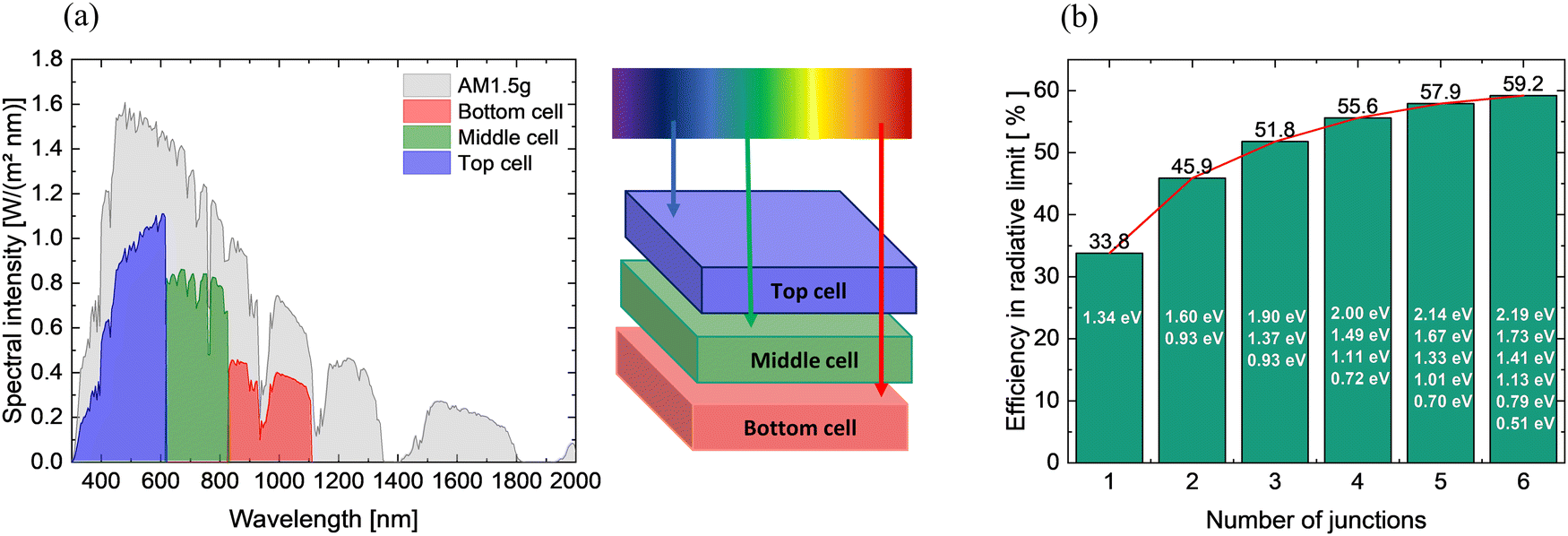 | ||
| Fig. 1 (a) Use of the solar spectrum by a triple-junction solar cell consisting of a silicon bottom cell, a 1.50 eV middle cell (e.g. GaInAsP), and a 2.00 eV top cell (e.g. AlGaInP). The transmission and thermalisation losses are reduced compared to single-junction and dual-junction solar cells. (b) Theoretical efficiency of multi-junction solar cells in the radiative limit as a function of the number of junctions. The optimum bandgpap combination is given for the maximum PCE under the AM 1.5g spectrum. The gain in efficiency becomes lower by increasing the number of junctions. Data taken from ref. 1. | ||
According to simulation by Philipps et al., the highest theoretical PCE that can be achieved in a detailed balance limit (Auger recombination is not taken into account) by a dual-junction solar cell is 45.9% under Air Mass 1.5 global (AM 1.5g) spectrum.1 This PCE limit can be exceeded by increasing the number of junctions in a solar cell. However, as shown in Fig. 1b the incremental increase becomes lower towards more junctions. Furthermore, the additional junctions introduce new challenges in terms of processing, choice of materials and interaction between the layers. Thus, triple-junction solar cells are a reasonable approach to achieve a good balance between efficiency potential, processing, and device complexity.
So far, highly efficient triple-junction solar cells are made of III–V semiconductor materials and are commercially available for concentrator photovoltaic and space application. Triple-junction solar cells using III–V materials reached 39.5% efficiency for a gallium indium phosphide (GaInP) top cell, gallium indium arsenide (GaInAs)/gallium arsenide phosphide (GaAsP) quantum well middle cell, and GaInAs bottom cell under the AM 1.5g spectrum.2 This exceeded the previous record of a sextuple-junction solar cell and made the triple-junction solar cell the most efficient non-concentrated terrestrial PV technology to date. Cells made from III–V compound semiconductor absorbers are highly efficient thanks to the low defect density that can be achieved in the single-crystalline materials and due to the direct nature of their bandgap. However, they require expensive deposition techniques such as metalorganic or hydride vapor phase epitaxy (MOVPE, HVPE) or molecular beam epitaxy (MBE) to achieve the required high crystal quality. The high production costs prevent these technologies from entering the terrestrial photovoltaic markets and consequently limit them to concentrator photovoltaic and space application where the high efficiency is the decisive factor. Several works have been done to couple III–V materials on a silicon bottom cell to reduce the cost and to benefit from the fact that the photovoltaic (PV) market is dominated by crystalline silicon. For the first time in 2013 Derendorf et al. reported successful integration of GaInP/GaAs//silicon in a triple-junction structure using wafer bonding.3 A record efficiency of 35.9% was achieved in 2021 for this type of solar cell.4 Technologically, wafer bonding is not favorable as it is an expensive serial process and requires an extra chemical-mechanical polishing (CMP) step.5 However, direct growth of III–V materials on silicon is also challenging due to lattice mismatch between the two materials and to date the efficiency of triple-junction solar cells by directly growing the III–V material on silicon is limited to 25.9%.6 A cheaper and yet promising alternative to III–V materials are metal halide perovskites. These materials have exceptional properties such as high absorption coefficient, long carrier diffusion length, direct bandgap, and high mobility of charge carriers.7–9 In addition, low cost, and simple fabrication methods as well as the ease of bandgap tuning make them ideal to be used in a multi-junction structure. Two-terminal perovskite-based dual-junction solar cells have shown significant efficiency improvement over the recent years with certified PCE of 28.0% for perovskite/perovskite,10 24.2% for perovskite/copper indium gallium selenide (CIGS)11 and 24.5% for perovskite/organic solar cells.12 Perovskite silicon dual-junction solar cells have reached 33.9% PCE13 which is higher than the efficiency of III–V based dual-junction solar cells and proves their great potential for the multi-junction concept.
Compared to the intense research on dual-junction perovskite-based solar cells, the research on its triple-junction structure is still at an early stage. Depending on the choice of the bottom cell, three types of triple-junction solar cells based on perovskite materials have been reported to date: (I) perovskite/perovskite/perovskite (known as all-perovskite), (II) perovskite/perovskite/silicon and (III) perovskite/perovskite/organic solar cells. The highest PCE reported is 23.3% for all-perovskite,14 22.2% for perovskite/perovskite/silicon,15 and 19.4% for the perovskite/perovskite/organic16 triple-junction solar cells. Among them only the 23.3% PCE reported for all-perovskite triple-junction solar cell is certified. Fig. 2 summarizes the evolution of triple-junction solar cells that have silicon and/or perovskite solar cells in their structure.
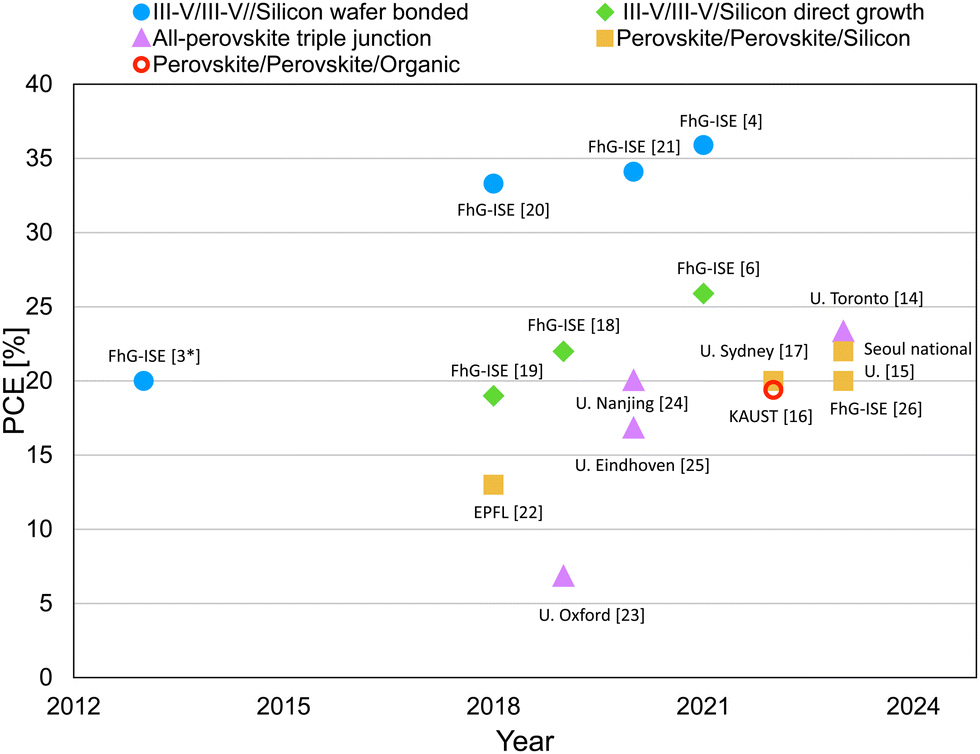 | ||
| Fig. 2 PCE evolution of two-terminal triple-junction solar cells with silicon and/or perovskite in their structure. Data taken from ref. 3, 4, 6 and 14–26. The record efficiency achieved for III–V/III–V/silicon solar cells are 35.9% and 25.9% using wafer bonding and direct growth respectively. The highest efficiency reported for all-perovskite triple-junction solar cell is 23.3%, for perovskite/perovskite/silicon is 22.2% (not certified) and for perovskite/perovskite/organic is 19.4% (not certified). All data are reported from measurement at AM 1.5g spectrum except for the first wafer bonded III–V/III–V//silicon which was measured at Air Mass 1.5 direct (AM 1.5d) spectrum *. | ||
In order to maximize the PCE of a triple-junction solar cell, appropriate bandgaps of the subcells should be combined. If there is no constraint in the bandgap of the bottom cell, the ideal combination of bandgaps that results in the maximum efficiency in a triple-junction solar cell are 0.93 eV, 1.37 eV, and 1.90 eV for bottom cell, middle cell, and top cell, respectively.1 A bottom cell with such a low bandgap is demonstrated with III–V materials.2 Perovskite solar cells with a bandgap around 1.20 eV14,24,25 and organic solar cells around 1.30 eV16 have been employed as bottom cells in triple-junction applications. Fig. 3 shows the theoretical PCE that can be achieved by a triple-junction solar cell with respect to the choice of the bottom cell. In addition, the optimum bandgap pairs for middle and top cells to maximize PCE in each structure is given in Table 1. Among these three types, perovskite/perovskite/silicon reaches a comparably high theoretical efficiency limit of 49% (neglecting Auger recombination), i.e., assuming a bottom cell absorber material with a direct bandgap of 1.10 eV. Moreover, high maturity of the silicon technology and its longevity make it most appealing for future market application.
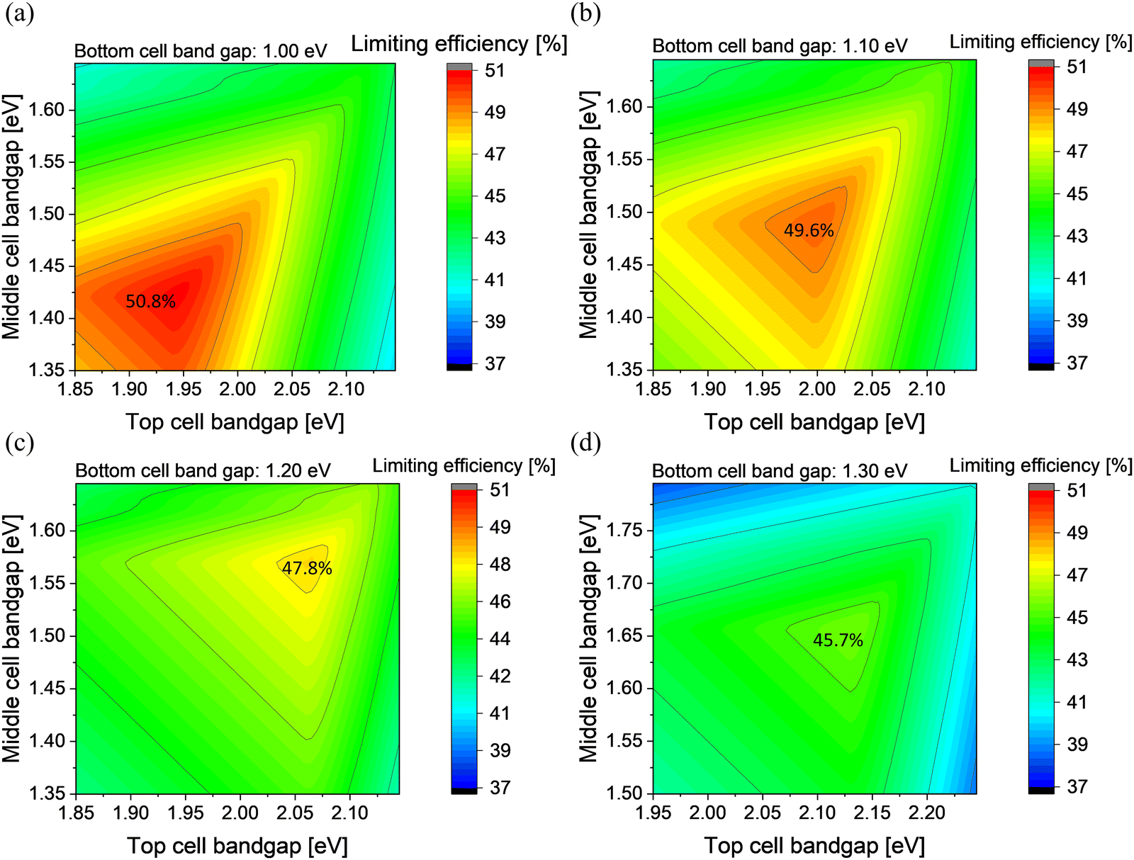 | ||
| Fig. 3 Theoretical efficiencies in the radiative limit for triple-junction solar cells for a bottom cell absorber with a bandgap of (a) 1.00 eV, (b) 1.10 eV, (c) 1.20 eV, and (d) 1.30 eV. The optimum top and middle cell bandgaps in each case are (a) 1.94 eV and 1.42 eV, (b) 2.00 eV and 1.49 eV, (c) 2.06 eV and 1.57 eV, and (d) 2.13 eV and 1.66 eV. | ||
| Bottom cell (eV) | Middle cell (eV) | Top cell (eV) |
|---|---|---|
| 1.00 | 1.42 | 1.94 |
| 1.10 | 1.49 | 2.00 |
| 1.20 | 1.57 | 2.06 |
| 1.30 | 1.66 | 2.13 |
It is important to note that the optimum bandgaps discussed are based on the theoretical efficiency limit, which does not necessarily give the maximum practical efficiency. In fact, Hörantner and Leijtens et al. assessed the practical potential of perovskite/perovskite/silicon triple-junction solar cells by combining optical and electrical simulation and reported an ideal combination of 1.44 eV and 1.95 eV for middle cell and top cell on a silicon bottom cell.27 In this simulation, optical and electrical losses such as parasitic absorption, series and shunt resistance derived from their experimental data are considered. Based on their simulation a 38.8% efficient perovskite/perovskite/silicon triple-junction solar cell can be achieved by optimizing charge extraction and recombination layers, while only 34.6% efficiency is feasible if absorbers with bandgaps limited to 1.50 eV and 2.00 eV are used. In a similar approach their simulation shows a 36.6% efficient all-perovskite triple-junction solar cell with a bandgap combinations of 2.04 eV, 1.58 eV, and 1.22 eV (Fig. 4).27 This change in optimum bandgap combinations based on more realistic assumption has also been previously reported on multi-junction solar cells of up to five junctions by taking non-radiative recombination of subcells into account.28 This indicates that the optimum combination of bandgaps is affected by properties of all layers and different loss mechanisms and should be determined according to each structure and choice of interlayer materials.
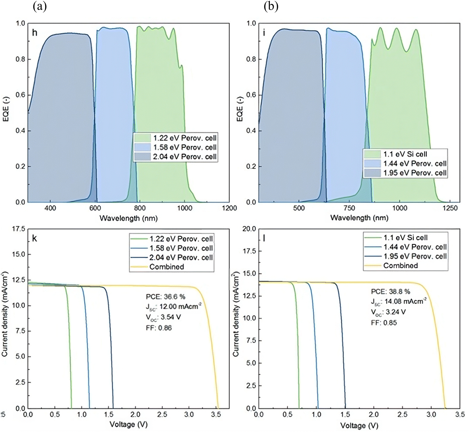 | ||
| Fig. 4 Simulated external quantum efficiency (EQE) and current density–voltage (jV) curves for maximum practical PCE (a) 36.6% for an all-perovskite triple-junction solar cell with perovskite's bandgaps of 1.22 eV, 1.58 eV, and 2.04 eV for the subcells and (b) 38.8% for a perovskite/perovskite/silicon triple-junction solar cell with bandgaps of 1.44 eV and 1.95 eV for perovskite subcells. Reproduced with permission from ref. 27, Copyright © 2017, American Chemical Society. | ||
Another important criterion in a series-connected multi-junction solar cell is current matching. In this type of solar cells, the current is limited by the subcell that generates the lowest current. Therefore, to maximize the current output of the solar cell, the current generated in each subcell should be the same.29 Achieving current matching in such a complex system is not trivial. In addition to bandgap adaptation, optimizing the thickness of absorber layers, reducing reflection losses as well as minimizing parasitic absorption of contact layers (e.g., thinning all the layers except for the absorber layers) is crucial. Even with the above mentioned considerations, the current matched device under standard test condition may not be current matched in the field as the spectra and temperature variations affect the bandgaps of the subcells in different ways.30–32 Furthermore, in a two-terminal configuration, the voltage of the final device is the sum of the voltages of all subcells. This means that to ensure highest voltage in the multi-junction solar cell, first the voltage deficit (i.e., Vdeficit = Eg/q − VOC, where Eg is the bandgap, q is the electron elementary charge and VOC the open-circuit voltage) of the individual subcells should be minimized and second lossless interconnection layers between the subcells are required.
So far, this introduction covered the potential of triple-junction solar cells based on simulation. Realization of such photovoltaic devices with maximum possible output in real lab conditions demands consideration of practical factors and limitations. Beyond optimization of individual layers, the processing sequence and layer interactions of the whole multilayer stack strongly influence the final device performance. Thus, a thorough analysis and comparison of the approaches taken for realizing the proof of concepts of these new technologies as well as follow-up studies are needed to allow fast technological development. This paper discusses the progress in engineering of monolithic perovskite-based triple-junction solar cells comprehensively. First, device architectures and interlayers used in current reported perovskite-based triple-junction solar cells including their photovoltaic parameters are summarized. Then, a review of perovskite absorbers suitable for middle cell and top cell together with details on bandgap tuning of perovskites, different deposition techniques, challenges associated with each type of the perovskite absorber, as well as possible strategies to tackle them are presented. In addition, we discuss the available materials and methods that are used for the recombination layers between perovskite subcells. Lastly, precise characterization of triple-junction solar cells based on the publications from current state-of-the-art III–V triple-junction technologies is adressed. Special emphasis is placed on potential uncertainties arising from measurements, along with suggestions on how to avoid them in research laboratories.
2. Perovskite-based triple-junction solar cells: categories and status
A monolithically integrated multi-junction solar cell consists of many layers processed sequentially on top of each other with different deposition methods. Process compatibility of each layer with its underlying layer is therefore of great importance. For example, solvent orthogonality, possible processing damage as well as thermal budget of the bottom layers should be considered when processing subsequent layers. Moreover, addition of each subcell increases the number of layers, which consequently introduces new challenges.Multi-junction solar cells can be divided into superstrate or substrate configuration (Fig. 5) depending on the type of bottom solar cell technology. In case of thin film bottom solar cells, such as in all-perovskite and perovskite/perovskite/organic solar cells, the superstrate configuration is used; solar cells are deposited on a glass (or foil) which is flipped and facing the sun in the final device. In case of wafer-based bottom solar cells, such as in perovskite/perovskite/silicon, the substrate configuration is used; the bottom cell wafer itself acts as the substrate and subsequent layers are processed on top. Consequently, the processing order of the absorbers is different. In the superstrate configuration, perovskites are processed in bandgap descending order and highest restrictions concerning process compatibility apply for the low bandgap perovskite absorber. In the substrate configuration, perovskite middle and top cells are processed successively on top of the bottom solar cell wafer. Highest restrictions concerning compatibility, such as annealing temperature and possible solution damage to the underlying layers apply for the processing of high-bandgap perovskite top cell. One example is high-temperature annealed nickel oxide (NiOx), that cannot be implemented as charge transport layer on top of another perovskite subcell. In addition, the first processed subcell (high bandgap in the superstrate and low bandgap in substrate configuration) must sustain several harsh conditions involved in the deposition of the top layers such as annealing steps, sputtering, etc. More discussion on fabrication of respective perovskite layers is presented in Section 3 and 4.
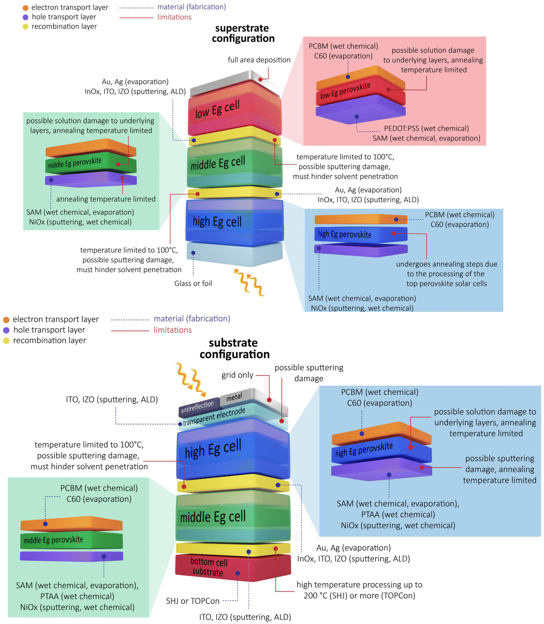 | ||
| Fig. 5 Schematic illustration of monofacial perovskite-based triple-junction solar cells with (top) superstrate configuration and (bottom) substrate configuration. Perovskite subcells are in p–i–n architecture. Some of the common materials for each layer together with their deposition techniques are shown. The processing of subsrate configuration starts with bottom cell (lowest bandgap subcell) while for superstrate configuration the top cell (the highest bandgap subcell) is processed first. The main limitations of the processes are highlighted. | ||
Moreover, perovskite solar cells can be classified by their order of deposition of the electron (n) and hole (p) transport and the perovskite absorber (i) layers into n–i–p (electron transport layer (ETL) deposited first) and p–i–n (hole transport layer (HTL) deposited first) device architectures. The work on perovskite/silicon tandem solar cells started on n–i–p architecture.33 However, the research focus changed toward the p–i–n structure due to an optically more favorable front contact, ease of fabrication and upscaling.
Similarly, the very first report on all-perovskite triple-junction solar cells in 2019 by McMeekin et al. had an n–i–p configuration implementing FA0.83Cs0.17Pb(Br0.70I0.30)3 (1.94 eV), MAPbI3 (1.55 eV) and MAPb0.75Sn0.25I3 (1.34 eV) perovskite absorbers.23 This work remains the only perovskite-based triple-junction solar cell with n–i–p architecture. Another exceptional approach regarding solar cell fabrication was that all the layers except for the silver electrode were solution-processed; even the indium tin oxide (ITO) recombination layer which is usually deposited via sputtering was replaced by spin coated ITO nanoparticles. Their strategy to overcome solvent compatibility issue was to change the conventional mixture of dimethylformamide/dimethyl sulfoxide (DMF/DMSO) as perovskite solvent to a new acetonitrile/methylamine (ACN/MA) solvent system for both low bandgap and middle bandgap perovskites. However, the change in solvent system yielded a reduced PCE. The triple-junction solar cell reached a PCE of 6.7% with an open-circuit voltage (VOC) of 2.70 V. The limited PCE mainly arose from low short-circuit current density (jSC) of 8.3 mA cm−2 limited by the low bandgap bottom cell, as well as a low fill factor (FF) of 43.0%. Other possible factors limiting the performance of this structure could be high parasitic absorption, especially in the 60 nm thick phenyl-C61-butyric acid methylester (PCMB) as ETL layer, and a high VOC deficit of the high bandgap perovskite top cell.
A year after this initial proof of concept, Wang et al. demonstrated an all-perovskite triple-junction solar cell in a p–i–n configuration based on Cs0.10(FA0.66MA0.34)0.90PbI2Br (1.73 eV), FA0.66MA0.34PbI2.85Br0.15 (1.57 eV), and FA0.66MA0.34Pb0.50Sn0.50I3 (1.23 eV) perovskite absorbers.25 They employed a two-step deposition method for processing of all three perovskite layers. Another noticeable improvement in their work came from introducing an optimized interconnection layer stack of tin oxide (SnOx)/gold (Au)/poly-(3,4-ethylendioxythiophen)-poly-(styrolsulfonat) (PEDOT:PSS) between the subcells which showed good solvent barrier function. In addition, they improved the ETL and replaced the 80 nm thick solution processed PCBM with a thinner layer of C60 (20 nm) deposited via thermal evaporation, which reduced parasitic absorption and charge accumulation in the interconnecting layers due to higher mobility of C60 compared to PCBM. As a result, the champion cell exhibited 16.8% PCE with a jSC of 7.3 mA cm−2, a VOC of 2.79 V, and a FF of 82.0%. The cell showed good stability during 300 s measurement at maximum power point. The high FF was the main factor that contributed to the PCE improvement compared to the previous work. The jSC of their device was limited by non-optimized bandgaps of the subcells as well as high parasitic absorption in ITO substrate and PEDOT:PSS layer.
Also in 2020, Xiao et al. reported a 20.1% efficient all-perovskite triple-junction solar cell by employing perovskites with Cs0.2FA0.8PbI0.9Br2.1 (1.99 eV), Cs0.05FA0.95PbI2.55Br0.45 (1.60 eV), and FA0.7MA0.3Pb0.5Sn0.5I3 (1.22 eV).24 The bandgap of the top cell was higher compared to the two previous publications which is more suitable for all-perovskite triple-junction solar cells. The champion device showed 20.1% PCE with a jSC of 8.8 mA cm−2, a VOC of 2.80 V, and a FF of 81.0%. The sample showed acceptable stability during 180 s of measurement at maximum power point in N2 environment. However, a longer measurement for 4000 s led to degradation of performance. A strategy developed in their work was the introduction of a double hole transport layer of nickel oxide (NiOx)/poly-[bis-(4-phenyl)-(2,4,6-trimethylphenyl)-amin] (PTAA) for the middle cell. Perovskite films typically feature a rough surface34,35 and it is challenging to form thin and conformal solution processed charge transport layers on top of them. Uncovered areas and pinholes can lead to shunting paths. Use of NiOx alone and in combination with organic HTL is found to be beneficial to fully cover the rough perovskite surface. In their triple-junction solar cell, 80 nm NiOx was deposited by spin coating of a pre-synthesized NiOx nanocrystal dispersion followed by 5 minutes annealing at 100 °C. The NiOx layer smoothened the surface and thus enabled improved spin coating of the thin PTAA layer on top. This strategy had been previously employed in a perovskite/CIGS tandem solar cell36 where Jost et al. deposited a 10 nm conformal NiOx layer by atomic layer deposition (ALD) without further annealing steps prior to deposition of PTAA, to avoid shunting in the perovskite cell processed on the rough CIGS surface.36 It is worth mentioning that some other perovskite-based triple-junction solar cells, from all three types, have also incorporated either NiOx alone or double hole transport layers with NiOx in their structure14,16,17 (Fig. 6).
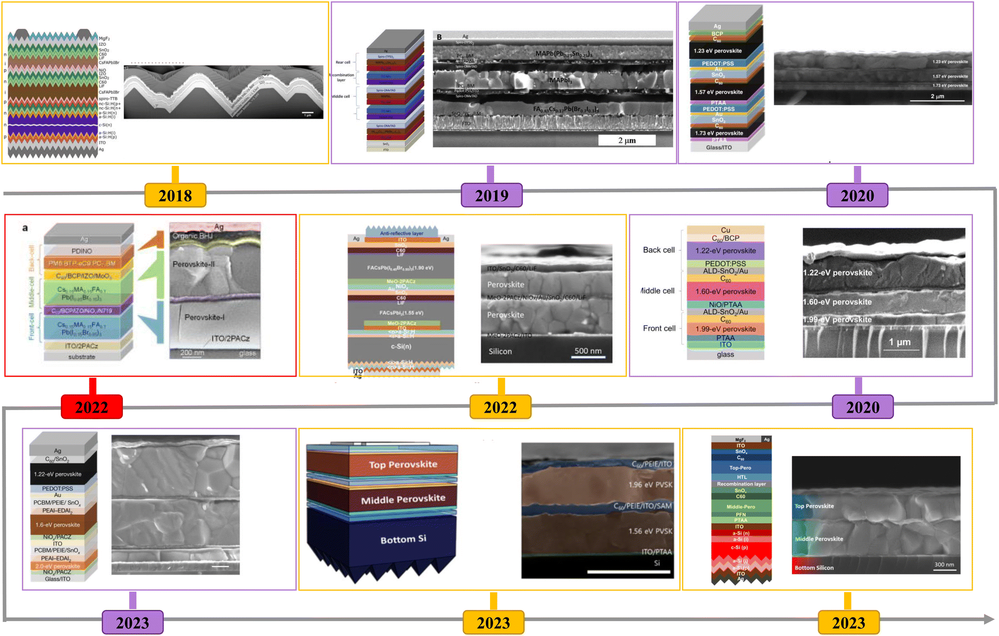 | ||
| Fig. 6 Structure evolution and cross sectional SEM images of perovskite-based triple-junction solar cells. Reproduced with permission from ref. 14–17, 22–26. Copyright © 2018, American Chemical Society. Copyright © 2019 Published by Elsevier Inc. Copyright © 2020, Wang et al., Published by Springer Nature, Copyright © 2020, American Chemical Society, Copyright © 2022, American Chemical Society, Copyright © 2022, American Chemical Society, Copyright © 2023,Wang et al. under exclusive licence to Springer Nature Limited, Copyright © 2023, American Chemical Society, Copyright © 2023 Heydarian et al., Published by American Chemical Society. | ||
Recently, Wang et al. published the first certified perovskite-based triple-junction solar cell.14 In this work, an all-perovskite triple-junction solar cell was made using Rb0.15Cs0.85PbI1.75Br1.25 (2.00 eV), Cs0.05FA0.90MA0.05Pb(I0.90Br0.10)3 (1.60 eV), and Cs0.05FA0.70MA0.25Pb0.50Sn0.50I3 with 5% SnF2 (1.22 eV) perovskite absorbers. This cell showed a certified PCE of 23.3%, a jSC of 9.6 mA cm−2, a VOC of 3.20 V and a FF of 76.2%. The encapsulated sample maintained 80% of its initial efficiency after 450 h of measurement in an ambient atmosphere. The main factor leading to this 23.3% efficient triple-junction cell was development of a rubidium (Rb), cesium (Cs) all-inorganic high bandgap perovskite absorber with improved stability. Details on this high bandgap perovskite are summarized in Section 4.3. Here, also a double HTL layer of NiOx/Me-4PACz was employed for both top and middle subcells. The high VOC of 3.2 V partially originated from the high-quality of the perovskite/charge transport layer interface. Me-4PACz has been shown to have a lossless interface with perovskite.37 In addition, in this work the perovskite/PCBM interface was passivated with phenethylammonium iodide and ethane-1,2-diammonium iodide (PEAI-EDAI2) to reduce the recombination loss at this interface. Moreover, to better protect the underlying layers, polyethyleneimine ethoxylated (PEIE) was spin coated on PCBM layer, prior to deposition of SnOx similar to the approach that has been previously reported by Palmstrom et al.38 As recombination layer between the top and middle cell, 20 nm of sputtered ITO was used whereas 1 nm evaporated Au served as the recombination layer between the middle and bottom cells. This work is the only perovskite-based triple-junction solar cell with certified efficiency.
The proof of concept for a perovskite/perovskite/silicon triple-junction solar cell was reported 1 year earlier than the all-perovskite triple-junction in 2018 by Werner et al. using a both-side textured silicon heterojunction (SHJ) bottom cell.22 In this work, perovskite solar cells had a p–i–n configuration. For deposition of perovskite layers on textured surfaces, a hybrid two-step deposition method was used, which the same group reported earlier for a both-side textured perovskite/silicon tandem solar cell.39 This hybrid method is a combination of co-evaporation of a scaffold of the inorganic precursors lead iodide (PbI2) and cesium bromide (CsBr) and subsequent spin coating of the organic precursors formamidinium iodide (FAI) and formamidinium bromide (FABr) from solution. Adaptation of the FAI/FABr ratio in the second step allows for control of the bandgap. The final perovskites had the general formula of CsxFA1−xPb(IyBr1−y)3 with non-specified values for x and y but bandgaps of 1.53 eV and 1.80 eV for middle and top cell absorbers, respectively. In this work, 150 nm indium zinc oxide (IZO) was used as a recombination layer between the two perovskite subcells. The champion cell exhibited 14.0% PCE with a FF of 68.0%, a VOC of 2.69 V and a jSC of 7.7 mA cm−2. The current of the final device was limited by the jSC of the middle cell. In order to estimate the ideal bandgap and thickness ranges for their material stack configuration, they performed optical simulations which showed that when the bandgap of the top cell is kept at 1.80 eV, the middle cell bandgap should be lowered to ∼1.40 eV to achieve current matching at a jSC of ∼12.2 mA cm−2 for a flat silicon bottom cell and a jSC > 13.0 mA cm−2 for a both-side textured bottom cell.
In 2022, Zheng et al. achieved 20.1% PCE for a perovskite/perovskite/silicon triple-junction solar cell.17 In contrast to the previous work, they employed solution-based spin coated perovskite absorbers on a SHJ bottom cell with flat front side and textured rear surface. Their champion device was based on a FA0.9Cs0.1PbI3 (1.55 eV) middle cell absorber and FA0.80Cs0.20Pb(I0.45Br0.55)3 (1.90 eV) top cell absorber and reached 20.1% PCE, 86.0% FF and 8.5 mA cm−2jSC with a VOC of 2.74 V. The cell showed acceptable stability measured for more than 40 s at maximum power point. In this work, 1 nm of Au was used as recombination layer between the perovskite subcells. The top perovskite absorber layer had a higher bandgap compared to the previous publication. This bandgap combinations for perovskite middle and top cells are closer to the optimum values suggested by simulations. As an antireflection layer, textured polydimethylsiloxane (PDMS) was used at the front side of the device. Overall, current matching was still not achieved in this work and the perovskite middle cell limited the jSC of the device.
Very recently, Choi et al. reported on a 22.2% perovskite/perovskite/silicon triple-junction solar cell15 on a flat front side and textured rear side SHJ. Perovskite middle and top cells in this work were Cs0.10FA0.85MA0.05PbI3 (1.56 eV) and MAPb(I0.50Br0.35Cl0.15)3 (1.96 eV), respectively. To avoid the solvent damage while processing the perovskite top cell, they followed a similar approach as the first all-perovskite triple-junction solar cell by McMeekin et al.23 They employed ACN/MA solvent system instead of DMF/DMSO for the top perovskite which was removed immediately after spin coating and prevented solvent penetration to the underlying layers. By taking advantage of this optimization, the perovskite top cell was fabricated without the ALD SnOx protection layer. Similar to the record all-perovskite triple-junction work,14 here PEIE was spin coated on top of C60. In addition, they employed a high-quality high bandgap perovskite achieved via additive engineering by adding urea into their perovskite precursor solution. With these two optimizations, the best performing cell showed 22.2% PCE, 78.6% FF and 10.2 mA cm−2jSC with a VOC of 2.78 V. The cell showed satisfactory stability for 600 s measured at maximum power point in ambient atmosphere at room temperature. The jSC of the final device was limited by the middle cell.
Our team recently fabricated perovskite/perovskite/silicon triple-junction solar cell with 20.0% PCE. A SHJ cell with flat front and textured rear side was employed as the bottom cell and perovskite middle and top cells were in p–i–n configuration similar to the previous works. Perovskite composition for the middle cell was Cs0.05(FA0.90MA0.10)0.95Pb(I0.95Br0.05)3 with a bandgap of 1.56 eV while the top perovskite absorber was a Cs0.05(FA0.55MA0.45)0.95Pb(I0.55Br0.45)3 perovskite with 1.83 eV bandgap. The champion cell exhibited 20.1% PCE with a FF of 78.1%, a jSC of 8.9 mA cm−2 and VOC of 2.87 eV. The open-circuit voltage was higher than the previously reported values for this structure. This has been achieved through optimizing the interconnection layers between the perovskite subcells with minimum voltage loss by replacing the Au/PTAA interlayer with ITO/2PACz as well as adapting the deposition technique for perovskite top cell to prevent solvent penetration to the middle cell. With regards to the latter, standard antisolvent deposition technique was replaced by an adapted gas quenching method. The solar cell showed acceptable stability for 360 s measured at fixed voltage close to the maximum power point voltage. In addition, for the first time the jV measurement of triple-junction perovskite-based solar cells were performed under a spectrum-adjusted solar simulator. More details on the measurement procedure are discussed in Section 6.2. Similar to the other reported perovskite/perovskite/silicon solar cells, the jSC of this device was limited by the middle cell.26
The only two-terminal perovskite/perovskite/organic triple-junction solar cell was developed by Isikgor and coworkers in 2022 with a p–i–n architecture achieving a VOC of more than 3.00 V. Cs0.15MA0.15FA0.70Pb(I0.15Br0.85)3 (2.05 eV) and Cs0.15MA0.15FA0.70Pb(I0.85Br0.15)3 (1.62 eV) were used as perovskite absorbers.16 A ternary organic bulk heterojunction (BHJ) PM6:BTP-eC9:PC71BM with 1.33 eV bandgap served as bottom cell. The champion perovskite/perovskite/organic triple-junction solar cell delivered a PCE of 19.4% with a VOC of 3.03 V, a jSC of 9.1 mA cm−2, and a FF of 70.4%. The cell showed satisfactory stability measured for 600 s at maximum power point in N2 environment. The limitation of their device stemmed mostly from the performance of the high bandgap perovskite top cell. Even though the VOC of this triple-junction solar cell is impressive through passivation of the top cell's perovskite/C60 interface with phenformin hydrochloride, it still can be improved by reducing the 0.78 V VOC deficit of the high bandgap perovskite.
The device structures and photovoltaic parameters VOC, jSC, FF and, PCE of the discussed perovskite-based triple-junction solar cells are summarized in Table 2.
| Year | 2018 | 2019 | 2020 | 2020 | 2022 | 2022 | 2023 | 2023 | 2023 | ||||||||||
| Triple Junction | Pero/pero/silicon | Pero/pero/pero | Pero/pero/pero | Pero/pero/pero | Pero/pero/silicon | Pero/pero/organic | Pero/pero/pero | Pero/pero/silicon | Pero/pero/silicon | ||||||||||
| Type | Substrate | Superstrate | Superstrate | Superstrate | Substrate | Superstrate | Superstrate | Substrate | Substrate | ||||||||||
| Structure | Texture SHJ/spiro TTB/1.53 eV pero/LiF/C60/SnOx/IZO/NiOx/1.8 eV pero/LiF/C60/SnOx/IZO/MgF2 | Glass/FTO/SnOx/PCBM/1.94 eV pero/spiro-OMeTAD/PEDOT:PSS/ITO/PCBM/1.55 eV pero/spiro-OMeTAD/PEDOT:PSS/ITO/PCBM/1.34 eV pero/spiro (TSFi)/Ag | Glass/ITO/PTAA/1.73 eV pero/C60/SnOx/Au/PEDOT:PSS/PTAA/1.57 eV pero/C60/SnOx/Au/PEDOT:PSS/1.23 eV pero/C60/BCP/Ag | Glass/ITO/PTAA/1.99 eV pero/C60/SnOx/Au/NiOx/PTAA/1.6 eV pero/C60/SnOx/Au/PEDOT:PSS/1.22 eV pero/C60/BCP/Cu | SHJ/ITO/MeO2PACz/1.55 eV pero/LiF/C60/SnO2/Au/NiOx/MeO-2PACz/1.9 eV pero/LiF/C60/SnOx/ITO/PDMS | Glass/ITO/2PACz/2.05 eV pero/Phen-HCl-C60/BCP/IZO/NiOx/N719/1.62 eV pero/C60/BCP/IZO/MoO3/1.33 eV organic/PDINO/Ag | Glass/ITO/NiOx/Me-4PACz/2.0 eV pero/PEAI-EDAI2/PCBM/PEIE/SnOx/ITO/NiOx/Me-4PACz/1.6 eV pero/PEAI-EDAI2/PCBM/PEIE/SnOx/Au/PEDOT:PSS/1.22 eV pero/C60/SnOx/Ag | SHJ/ITO/PTAA/1.56 eV pero/C60/PEIE/ITO/Me-4PACz/1.96 eV pero/C60/PEIE/ITO/Ag | SHJ/ITO/PTAA/PFN/1.56 eV pero/C60/SnOx/ITO/2PACz/1.83 eV pero/C60/SnOx/ITO/Ag/MgF2 | ||||||||||
| Config | p–i–n | n–i–p | p–i–n | p–i–n | p–i–n | p–i–n | p–i–n | p–i–n | p–i–n | ||||||||||
| Scan direction | Reverse | Forward | Reverse | Forward | Reverse | Forward | Reverse | Forward | Reverse | Forward | Reverse | Forward | Reverse | Forward | Certified | Reverse | Forward | Reverse | Forward |
| PCE (%) | 14.0 | 12.1 | 6.7 | NA | 16.8 | 16.4 | 20.1 | 19.9 | 20.1 | NA | 19.4 | 19.2 | 24.3 | 24.3 | 23.3 | 21.8 | 22.2 | 20.1 | 20.0 |
| FF (%) | 68.0 | 58.7 | 43.0 | NA | 82.0 | 81.0 | 81.1 | 80.7 | 86.0 | NA | 70.4 | 69.6 | 77.9 | 78.7 | 76.2 | 76.9 | 78.6 | 78.1 | 77.9 |
| j SC (mA cm−2) | 7.7 | 7.7 | 8.3 | NA | 7.3 | 7.3 | 8.8 | 8.8 | 8.5 | NA | 9.1 | 9.1 | 9.7 | 9.6 | 9.6 | 10.2 | 10.2 | 8.9 | 8.9 |
| V OC (V) | 2.69 | 2.69 | 2.70 | NA | 2.79 | 2.77 | 2.80 | 2.80 | 2.74 | NA | 3.03 | 3.03 | 3.20 | 3.20 | 3.20 | 2.78 | 2.78 | 2.87 | 2.86 |
| Area (cm2) | 1.420 | 0.092 | 0.068 | 0.049 | 1.030 | 0.100 | 0.049 | NA | 1.000 | ||||||||||
| Ref. | 22 | 23 | 25 | 24 | 17 | 16 | 14 | 15 | 26 | ||||||||||
3. Suitable perovskite absorbers for middle cell application
As mentioned in Section 1, in a triple-junction solar cell the optimum bandgap for the middle cell is in the range of 1.40–1.65 eV, depending on the choice of the bottom cell. This range overlays well with the current absorbers used in high-efficient single-junction devices; therefore, development of the middle cell perovskite can strongly benefit from previous research in the field.Perovskite has a general formula ABX3 where A is a monovalent organic or inorganic cation such as methylammonium (MA), formamidinium (FA), and cesium (Cs). B is typically divalent lead (Pb) or tin (Sn) and X is a halide, mostly iodide (I) and bromide (Br) or a combination of them.7 One outstanding property of metal halide perovskite is their bandgap tunability, which makes them ideal to be used in multi-junction solar cells. The perovskite's bandgap can be tuned from 1.2 eV to 3.1 eV40 by compositional engineering via cation or halide substitution (Fig. 7).34,40–43
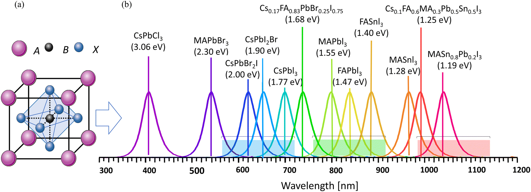 | ||
| Fig. 7 (a) ABX3 structure of perovskite material where A is a monovalent organic or inorganic cation such as methylammonium (MA), formamidinium (FA), and cesium (Cs). B is typically divalent lead (Pb) or tin (Sn) and X is a halide, mostly iodide (I) and bromide (Br) or a combination of them. (b) Perovskite bandgap tunability in the range from 1.2 eV to 3.1 eV. The bandgap range suitable for top cell, middle cell and bottom cell are highlighted by blue, green and red background accordingly. Adapted with permission from ref. 40 and 47 Copyright © 2020 Elsevier Inc and ref. 47 available from: https://doi.org/10.1021/nl5048779, Copyright © 2019 American Chemical Society. | ||
Primarily, the perovskite's bandgap is determined by the B- and X-site ions forming a [BX6] octahedral framework. The valence band maximum (VBM) consists of B-s and X-p orbital coupling, while CBM consists mainly of B-p orbital contribution.44 The A-site cation has ionic character and its electronic states do not contribute to the VBM or CBM.45 Nonetheless, the A cation can influence the [BX6] framework sterically or electrostatically. In this way, expansion or tilting of the lattice structure can lead to changes in the bandgap.46 Depending on the B-site cation used (Pb or Sn), smaller cations on the A-site (Cs < MA < FA) can either increase or reduce the bandgap.46 Most commonly, A- and X-sites are tuned at the same time to adjust the bandgap and ensure phase stability of the final composition.
The first reported perovskite solar cell was MAPbI3 absorber with a bandgap of 1.55 eV,48 however it is not regarded as promising middle cell absorber due to poor moisture and thermal stability above 85 °C.49 Improved performance as well as chemical and thermal stability have been achieved for multi cation (Cs/MA/FA) multi halide (Br/I) perovskite compositions that are now widely used in the community.50
3.1 Middle perovskite subcell in current triple-junction solar cells
The record PCE of p–i–n perovskite single-junction solar cells is 24.7% using a triple cation double halide absorber with a Cs0.05(FA0.95MA0.05)0.95Pb(I0.95Br0.05)3 composition and a 1.55 eV bandgap.51 Currently the perovskite middle cells in reported triple-junction solar cells have bandgaps in the range of 1.55 eV to 1.62 eV. Table 3 summarizes compositions and bandgaps of the middle perovskite absorbers implemented in current triple-junction solar cells, as well as device structures and jV performances of respective single-junction solar cells.| Year | 2019 | 2020 | 2020 | 2022 | 2022 | 2023 | 2023 | 2023 |
| Composition | MAPbI3 | FA0.66MA0.34PbI2.85Br0.15 | Cs0.05FA0.95PbI2.55Br0.45 | Cs0.1FA0.9PbI3 | Cs0.15MA0.15FA0.70Pb(I0.85Br0.15)3 | Cs0.05FA0.9MA0.05Pb(I0.9Br0.1)3 | Cs0.1FA0.85MA0.05PbI3 | Cs0.05(FA0.9MA0.1)0.95Pb(I0.95Br0.05)3 |
| Bandgap (eV) | 1.57 | 1.57 | 1.60 | 1.55 | 1.62 | 1.60 | 1.56 | 1.56 |
| Structure | Glass/FTO/SnOx/PCBM/perovskite/spiro-OMeTAD/Ag | Glass/ITO/PTAA/perovskite/C60/BCP/Al | Glass/ITO/NiOx/PTAA/perovskite/C60/BCP/Cu | Glass/ITO/HTL/perovskite/LiF/C60/BCP/Cu | Glass/ITO/NiOx/N719/perovskite/C60/BCP/Ag | Glass/ITO/NiOx/Me-4PACz/perovskite/PEAI-EDAI2/PCBM/PEIE/SnOx/Ag | Glass/ITO/PTAA/PFN-Br/perovskite/C60/PEIE/Ag | Glass/ITO/PTAA/PFN-Br/perovskite/C60/SnOx/Ag/MgF2 |
| Molarity (M) | 1.03![[thin space (1/6-em)]](https://www.rsc.org/images/entities/char_2009.gif) :1 MAI:PbI2 :1 MAI:PbI2 |
NA | 1.40 | 1.50 | 1.25 | 1.50 | 1.40 | 1.20 |
| Thickness (nm) | 530 | 450 | 280 | NA | NA | 780 | NA | 450 |
| PCE (%) | 15.3 | 16.5 | 19.4 | 18.1 | 21.0 | 21.1 | 20.1 | 15.6 |
| FF (%) | 70.0 | 76.0 | 80.2 | 78.0 | 79.4 | 77.3 | 80.3 | 77.2 |
| j SC (mA cm−2) | 20.8 | 21.0 | 22.4 | 23.3 | 22.4 | 22.5 | 24.5 | 19.8 |
| V OC (V) | 1.06 | 1.03 | 1.08 | 1.01 | 1.18 | 1.20 | 1.04 | 1.02 |
| Top cell in | Pero/pero/pero | Pero/pero/pero | Pero/pero/pero | Pero/pero/silicon | Pero/pero/organic | Pero/pero/pero | Pero/pero/silicon | Pero/pero/silicon |
| Ref. | 23 | 25 | 24 | 17 | 16 | 14 | 15 | 26 |
As mentioned before, so far, the reported perovskite/perovskite/silicon triple-junction solar cells suffer from current mismatch in a way that the middle cell is limiting the overall current of the device and highest current is being generated in the silicon bottom cell. For improved current matching, reducing the bandgap of the middle cell perovskite absorber is required. In the following sections, we discuss the two most promising perovskite candidates with bandgap lower than 1.50 eV.
3.2 Strategies for stable FAPbI3 perovskite with bandgap of 1.47 eV
Compared to MAPbI3, implementing FA on the A-site allows to form a nearly cubic structure, a reduced bandgap (1.47 eV), and improved thermal stability.52,53 Moreover, its bandgap is ideal to be used as middle cell absorber in a triple-junction structure with a 1.12 eV bottom cell. The work on FAPbI3 solar cell has mostly been in the n–i–p architecture which holds the record single-junction perovskite solar cell with a PCE of 25.8%.54 Despite the relatively fewer works on the FAPbI3 based p–i–n solar cells, recently an impressive PCE of 24.1%55 has been reported, which is promising for multi-junction solar cell's application.The major challenge of FAPbI3 perovskite lies in its limited structural stability. Due to disordered FA-I ion interaction, the asymmetrical FA cation takes an off-centered position, which results in the formation of a trigonal instead of a cubic structure. Experimentally, a 1D yellow non-perovskite polymorph (yellow δ-phase) is formed for usual low-temperature annealing around ∼100 °C. Annealing at 160 °C allows to form the desired cubic phase (black α-phase),56 which could harm temperature-sensitive underlying layers. Moreover, exposure to ambient environment, particularly high humidity, can trigger the phase transition from black α- to yellow δ-phase.56
Fig. 8 shows the PCE evolution of FAPbI3 perovskites for n–i–p and p–i–n structures.
 | ||
| Fig. 8 PCE evolution of FAPbI3 solar cells in p–i–n and n–i–p configuration discussed in this review for different strategies that resulted in efficient solar cells and improved stability (red: compositional engineering, orange: deposition technique, green: additive engineering, blue: surface and interface passivation and purple: charge transport layer). Data for n–i–p configuration are taken from ref. 54 and 57–64 and for p–i–n configuration from ref. 55 and 65–68. Certified values are marked with #. | ||
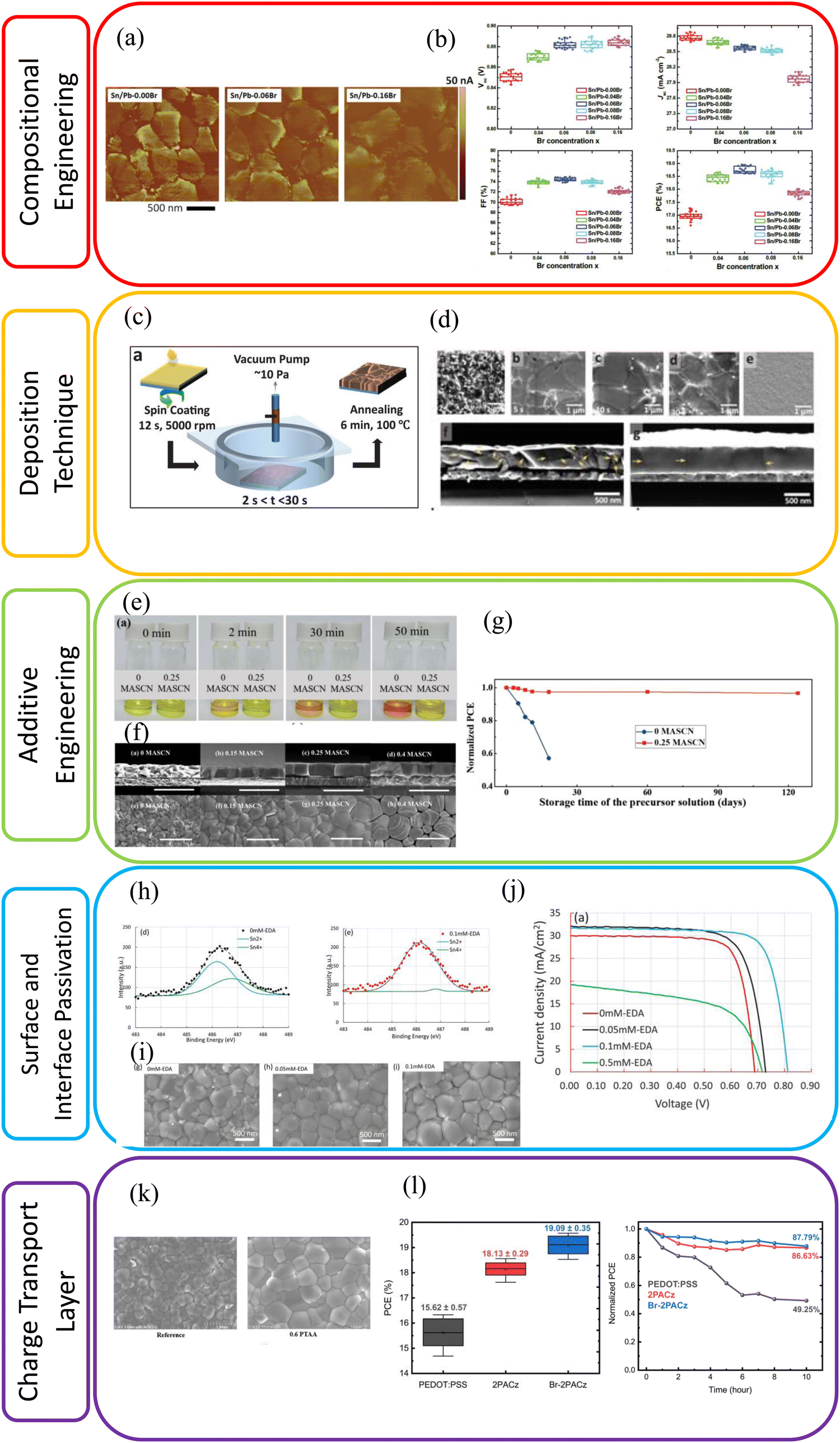
In order to improve the stability of FAPbI3 and achieve the black perovskite phase at low annealing temperature several strategies have been reported in the literature, which we briefly summarize below:
(1) Compositional engineering: the most famous approach to stabilize the black α-phase is alloying a small concentration of cations and anions with smaller ionic radius such as MA, Cs and Br to the composition. For example, Lee et al. showed that by adding a small amount of CsI to FAPbI3, a black perovskite phase can be formed even prior to the annealing step.69 This approach however has the drawback of increasing the bandgap of perovskite. Min et al. reported stable α-FAPbI3 by incorporation of small amount of methylenediammonium dichloride (MDACl2) into perovskite lattice. The film annealed for 10 minutes at 150 °C, showed almost identical bandgap compared to the control film, and the corresponding solar cell delivered 23.7% certified efficiency. This perovskite solar cell retained 90% of its PCE for 20 h in air under 150 °C with no encapsulation.58 Moreover, non-stoichiometric modified precursors have shown several advantages in film quality of different perovskite compositions. For FAPbI3 perovskite, excess FAI resulted in formation of the black film at low annealing temperature of 60 °C70 or even without annealing at room temperature.71 Zhang et al. systematically studied the effect of excess PbI2 in FAPbI3 precursor solution and found that it reduced charge trap densities and prolonged charge carrier lifetimes.66 Previous studies have confirmed the impact of excess PbI2 in passivating the grain boundaries of perovskite.72
(2) Deposition technique: the fabrication method employed to deposit the perovskite layer is known to influence film crystallization. Instead of common one-step spin coating deposition, a two-step sequential deposition is found to form stable α-phase FAPbI3 at low annealing temperature of 80 °C.73 In this technique, PbI2 is first deposited and then FAI solution is processed on top. It is crucial to obtain a highly porous thin film of PbI2 in first place to form stable phase-pure α-FAPbI3.74 Xu et al. showed that by using DMF/N-methyl-2-pyrrolidone (NMP) solvent mixture for PbI2, a porous morphology can be achieved. In addition, they introduced a dynamic spin coating method in which a pure α-phase FAPbI3 film formed even prior to the annealing step.74 Huang et al. used a mixture of isopropanol/hexafluorobenzene solvent for the organic salt of the second step and achieved a very high efficiency of 25.8% which retained 94% of its efficiency for more than 1000 h of MPP tracking.54 Vacuum deposition is an alternative method to conventional solution processing. Borchert at al. showed that by co-evaporation of FAI and PbI2, homogeneous and pinhole-free FAPbI3 film can be formed. They demonstrated that in contrast to the standard solution processing which requires long annealing steps, here only a very short annealing time of 1 minute at 170 °C was needed to convert δ-phase of FAPbI3 to the desired α-phase.75
(3) Additive engineering is reported to enhance phase stability of FAPbI3 by improving perovskite crystallization and defect passivation. For example, adding methylammonium chloride (MACl) into the perovskite precursor solution has been reported in both inverted67 and regular54,63,76 architectures. Park et al. reported a 25.7% PCE by adding propylammonium chloride (PACl) as a secondary additive to the FAPbI3 with MACl additive.64 Jeong et al. added 2% formamidine formate (FAHCOO) which is a pseudo-halide additive into the precursor solution and reported a certified PCE of 25.2% for a FAPbI3 perovskite solar cell with improved operational stability over 450 h with no encapsulation.60 Jiang et al. incorporated methylamine formate (MAFa) ionic liquid into FAPbI3 perovskite which resulted in crystallinity and morphology improvement and increase of charge carrier lifetime. As a result, record PCE of 24.1% for inverted architecture was achieved. In addition, this strategy led to prolong stability against moisture with only 10% loss of PCE after storing the sample for 1000 h in ambient without encapsulation.55 Furthermore, adding CsPbBr363 and MAPbBr357 into FAPbI3 solution are reported to reduce the deep level defects concentration and increase the performance.
(4) Interfacial and surface passivation: interfacial treatment by formation of thin two-dimensional perovskite capping layers, between the 3D perovskite and the subsequent charge transport layer can protect FAPbI3 from moisture penetration and stabilize its α-phase. Wang et al. demonstrated that post treatment of the perovskite surface with cyclopropylcarbamidine hydrochloride (CPAH) resulted in formation of a hydrophobic 2D layer of (CPA)2PbI2Cl2 on top of the perovskite surface which significantly improved the stability of the solar cells against humidity. CPAH treated samples retained 74% of the initial PCE after 150 h storage in ambient environment.77 In a similar approach Kareem et al. treated FAPbI3 surface with a 2-(4-fluorophenyl) ethyl ammonium iodide (FPEAI). The PCE of the not-passivated device maintained only 46% of its initial PCE, while the device with FPEAI showed 80% of its efficiency during more than 1000 h measurement due to the formation of 2D/3D heterostructure.62
(5) Charge transport layer: the charge transport layer plays an important role on phase stability of FAPbI3 films. Roß et al. studied the effect of the HTL on phase stability of co-evaporated FAPbI3 in p–i–n configuration and demonstrated that free phosphonic acids groups of the self-assembling molecule MeO-2PACz significantly improved the stability of the black FAPbI3 perovskite phase.71 Zhang et al. also compared the effect of different commonly used HTL materials in p–i–n configuration: PEDOT:PSS, PTAA, NiOx, and MeO-2PACz in FAPbI3 solar cells. Similarly, they reported that devices with MeO-2PACz showed higher PCE and much longer stability as 92% of the PCE was retained after 800 h storage at room temperature and high humidity with no encapsulation.66 Min et al. reported a 25.5% FAPbI3 solar cell which was achieved by chemical passivation of perovskite/ETL interface in an n–i–p configuration. By coating a Cl-containing perovskite on a Cl-bonded SnOx, a FASnClx interlayer was formed between the perovskite and the underlying ETL. The successful passivation not only resulted in improved charge extraction and reduced non-radiative recombination but also led to better long term stability (90% of the initial PCE was retained after 500 h of MPP tracking) of the device with no encapsulation.61 A study by Jeong et al. compared Spiro-OMeTAD, Spiro-mF and Spiro-oF as HTLs and showed that the fluorination of Spiro-OMeTAD helps to achieve high-efficient FAPbI3 cells with improved stability (Fig. 9).59
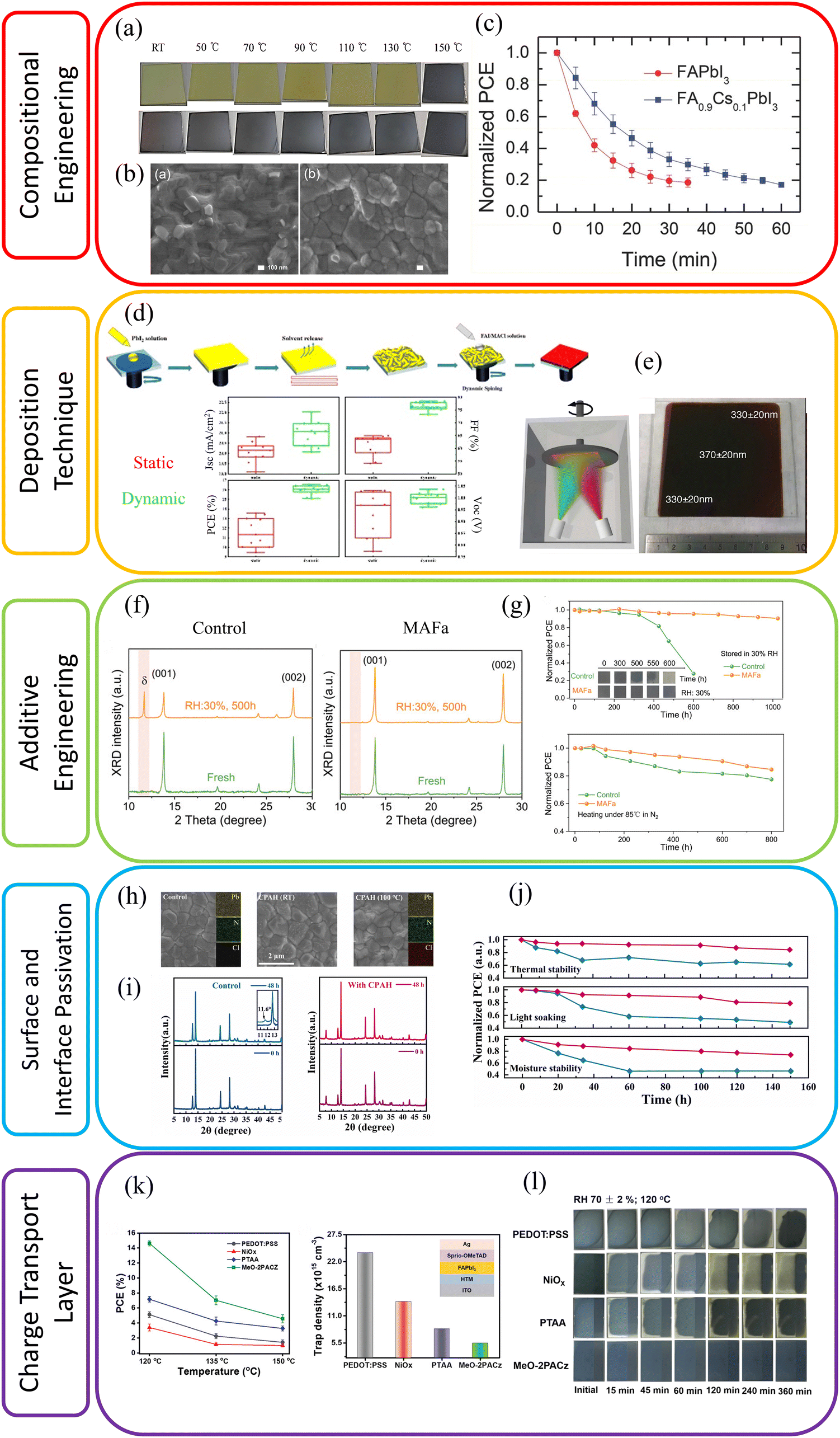 | ||
| Fig. 9 General approaches reported in literature to improve performance and stability of FAPbI3 perovskite solar cells. (a) FAPbI3 and FA0.9Cs0.1PbI3 films with different annealing temperatures, (b) Top view SEM images of FAPbI3 and FA0.9Cs0.1PbI3 and (c) normalized PCE of their respective solar cells without encapsulation measured over time in ambient. Cs incorporation resulted in formation of black perovskite even at room temperature. FA0.9Cs0.1PbI3 has improved film quality and stability compared to pure FAPbI3. Reproduced with permission from ref. 69. Copyright © 2015 WILEY-VCH Verlag GmbH & Co. KGaA, Weinheim. (d) Schematic illustration of perovskite processing of FAPbI3 solar cells processed with 2-step deposition method using dynamic spin coating for the organic salt and statistical photovoltaic parameters (jSC, PCE, FF and VOC) of FAPbI3 solar cells comparing static and dynamic spin coating for organic salt deposition. Reproduced with permission from ref. 74. Copyright © 2022, Rights managed by AIP Publishing. (e) Schematic illustration of evaporation method for processing of FAPbI3 and respective FAPbI3 film processed on large area with this method. Black FAPbI3 is formed after 1 minute annealing at 170 °C. Reproduced with permission from ref. 75 Copyright © 2017, American Chemical Society. (f) XRD measurement of fresh and aged FAPbI3 films with and without MAFa additive and (g) operational and thermal stability of FAPbI3 solar cells with and without MAFa additive. Adding MAFa into perovskite precursor leads to excellent phase stability for 500 h and the corresponding solar cell exhibited improved operational stability. Reproduced with permission from ref. 55. Copyright © 2023 Wiley-VCH GmbH. (h) Top view SEM images of FAPbI3 films with and without passivation with CPAH, (i) XRD measurement of fresh and aged FAPbI3 films with and without CPAH treatment and (j) operational and thermal stability of FAPbI3 solar cells with and without passivation. Passivating the perovskite surface with CPAH resulted in phase stability for 48 h and the corresponding solar cell exhibited improved operational stability. Reproduced with permission from ref. 77. Copyright © 2021 Elsevier Ltd. All rights reserved. (k) PCE of FAPbI3 solar cell in p–i–n configuration using different HTLs and varied annealing temperature along with the trap density calculated for perovskite films on different HTLs and (l) perovskite films with different HTLs kept under 70% RH and 120 °C condition. Solar cell with MeO-2PACz as HTL indicated highest PCE and lowest trap density. The FAPbI3 perovskite deposited on MeO-2PACz was more stable compared to other HTLs. Reproduced with permission from ref. 66. Copyright © 2022 Wiley-VCH GmbH. | ||
More detailed reviews on FAPbI3-based perovskites as well as strategies to overcome the challenges associated with them are presented in recent review articles.53,56,78,79
3.3 Strategies for stable Pb–Sn perovskite with bandgaps below 1.47 eV
Further lowering the bandgap of perovskite is possible by complete or partial substitution of Pb with Sn in B-site cation, which directly alters the conduction band.44,80,81 Sn-containing perovskites with mixture of halides in the composition (Br/I) cover a broad bandgap range from 1.2 eV to 2.0 eV.82 The reduction of bandgap however does not follow a linear trend when substituting Pb with Sn;80,81 studies have shown that in mixed Sn–Pb perovskites the bandgap continuously reduces by increasing Sn content and reaches its minimum at approximately 80% Sn content and then widens afterwards. Thus, MAPb0.20Sn0.80I3 shows a lower bandgap of 1.19 eV compared to MASnI3 with 1.28 eV bandgap.80 Sn-based perovskite solar cells were first explored in 201283 and significant progress has been made ever since; in 2023 the PCE of Sn-containing perovskite increased to 23.7% using a Cs0.2FA0.8Pb0.5Sn0.5I3 (1.29 eV) absorber.84Fig. 10 shows the PCE evolution of Pb–Sn perovskites along with their corresponding compositions and bandgaps.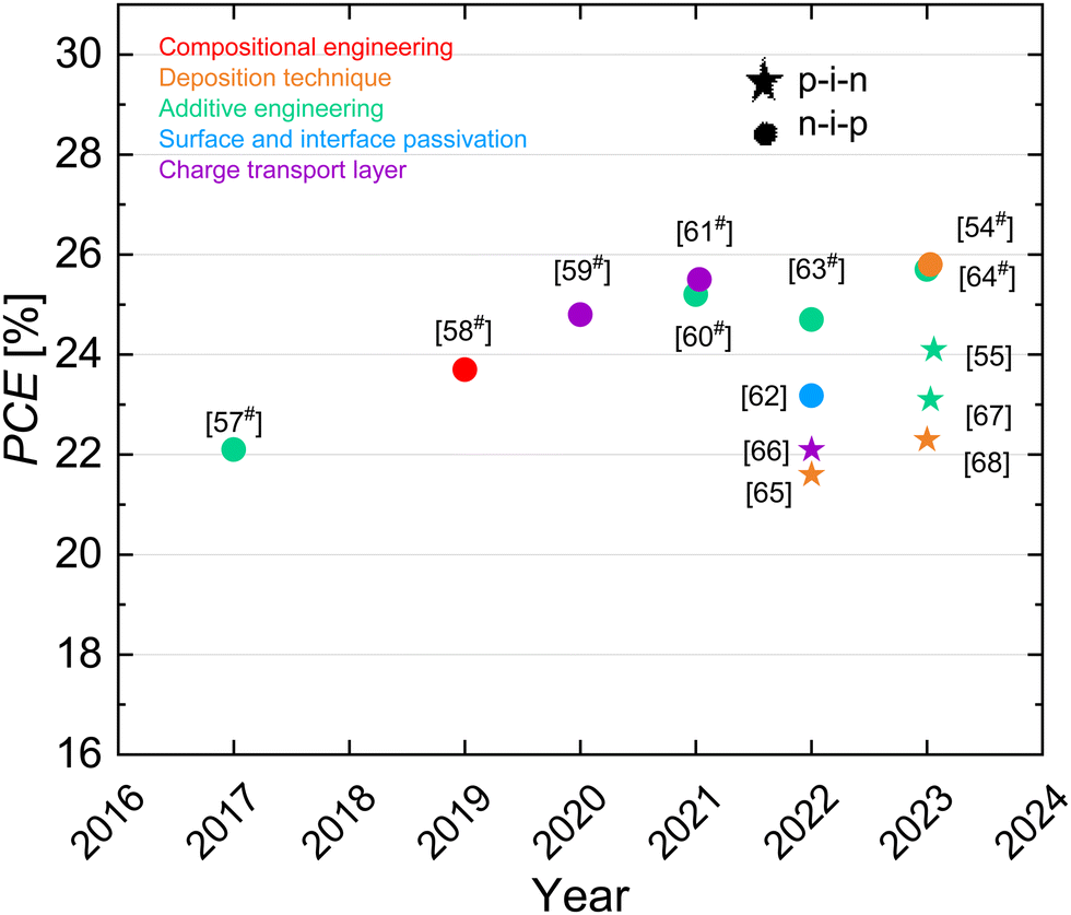 | ||
| Fig. 10 Composition, bandgap and PCE evolution of Sn-containing perovskites discussed in this review for different strategies that resulted in efficient solar cells and improved stability (red: compositional engineering, orange: deposition technique, green: additive engineering, blue: surface and interface passivation and purple: charge transport layer). Data are taken from ref. 84–92. Certified values are marked with #. | ||
Sn-containing perovskite absorbers have been widely used as low bandgap bottom cell in all-perovskites dual-junction and recently triple-junction devices. The community therefore has focused on perovskites with low bandgap ∼1.20 eV; less research is available on Sn-based perovskites with bandgaps above 1.35 eV suitable for the middle cell in triple-junction devices. Among them, pure Sn perovskite with FASnI3 composition could be an attractive option. First, its bandgap of ∼1.40 eV is suitable for the middle cell of triple-junction solar cell especially on top of silicon bottom cell, and secondly, employing such Pb-free perovskite in multi-junction solar cell relaxes the concern regarding the toxicity of Pb. However, the maximum certified PCE reported so far for FASnI3 solar cell is 14.1%92 which lags behind the performance of pure Pb and Pb–Sn perovskites.
In general, there are two major challenges associated with Sn-containing perovskite. First, Sn2+ can easily be oxidized to Sn4+ in the presence of small amounts of oxygen leading to defect formation that reduces carrier lifetime.93 Second, due to non-uniform nucleation and fast crystallization of Sn-containing perovskite, fabrication of high-quality, homogeneous, compact, and pinhole-free film is more challenging compared to pure Pb perovskite.91,94 Such non-ideal perovskite films with defects and large number of grain boundaries in turn accelerate the oxidation of Sn2+. Klug et al. reported that the photoluminescence intensity of perovskite film decreased by orders of magnitude when replacing only 1% of the Pb with Sn in the composition, which proves the challenges on the way of bringing Sn-based perovskite to the level of pure Pb perovskite.95
Some strategies reported in literature to overcome these challenges are:
(1) Compositional engineering: perovskite composition and solution preparation have a crucial impact on the quality of the perovskite film in general and consequently the device performance. This is particularly critical in the case of Sn-based perovskites since they are prone to defects as discussed before. Usually, the perovskite solution is prepared by dissolving the precursor powders in an appropriate solvent. Liao et al. introduced a new precursor system by preparing FASnI3 and MAPbI3 precursor solutions separately and mixed them subsequently at different molar ratios. The fabricated (FASnI3)0.6(MAPbI3)0.4 perovskite films showed dense grains with no visible pinholes.96 Li et al. demonstrated that incorporation of Br in mixed Pb–Sn perovskite improves perovskite film quality and effectively passivates the grain boundaries. Optimizing Br concentration to 6% led to 19.0% PCE.89 In another approach incorporation of Cs into FA0.8MA0.2Sn0.5Pb0.5I3 perovskite improved the operational stability and for the optimum Cs content of 2.5%, PCE of 18.2% was reported.97
(2) Deposition technique: as discussed in the previous section, fabrication method can have a huge impact on morphology of the formed perovskite film. Abdollahi Nejand et al. introduced processing of Sn-containing perovskite films via the vacuum-assisted growth control (VAGC). In this method, instead of using an antisolvent, a vacuum chamber is used to remove the solvents from the film. As a result of process optimization, homogeneous pinhole-free perovskite layers with large grains were achieved.94 Werner et al. employed the gas quenching method, in which a flow of nitrogen is used to remove the solvent from the film. Sn-containing perovskite films processed with N2 quenching also showed uniform, pinhole-free morphology.91 The improvement in morphology was shown to reduce defects at the grain boundaries and is a crucial factor to improve the performance and stability of Sn-containing perovskites.98
(3) Additive engineering: introducing inorganic Sn halide additives SnX2 (X = F, Cl, Br, I) into the precursor solution has widely been reported to limit the oxidation by reducing the formation of Sn vacancies. For example, employing SnF2 additive resulted in better crystallization and formation of pinhole-free perovskite layer.99 Incorporation of a small amount of metallic Sn powder not only helps to lower the oxidation of Sn2+ to Sn4+ but also is a step further and can convert Sn4+ back to Sn2+.87 Organic additives such Guanidinium thiocyanate (GuaSCN)100 and methylammonium thiocyanate (MASCN)101 have also been reported to increase the perovskite grain size and reduce the grain boundaries. In addition Sn2+ and SCN− interaction has shown to inhibit the degradation of Pb–Sn perovskite precursor.101 Xiao et al. added zwitterionic antioxidant into the perovskite precursor solution.86 The zwitterionic molecules hindered Sn2+ oxidation and passivated defects at the surface and grain boundaries of mixed Pb–Sn perovskite films, leading to certified PCE of 20.7%.86 Furthermore, introducing hydrazine sulfate (HS) additive into Sn-containing perovskite has been found to slow down the crystallization. This in turn resulted in homogeneous distribution of elements and high quality perovskite film which led to 23.2% PCE.102 Very recently 23.7% PCE was achieved for Pb–Sn perovskite by improving the film quality through addition of octyl ammonium tetrafluoroborate (OABF4) into the perovskite precursor.84
(4) Interfacial and surface passivation: oxidation of Sn mostly occurs at the perovskite surface. Therefore, passivating the surface with different treatment methods such as forming 2D/3D structure can protect the perovskite surface and reduce the degradation rate by blocking the diffusion of oxygen into the grains. Kapil et al. studied the effect of surface treatment of Pb–Sn perovskite with ethylenediamine (EDA). They showed that the EDA treated perovskite films had reduced Sn4+ concentration on their surface compared to the non-treated films. The champion cell with optimum EDA concentration showed 21.7% PCE.103 Hu et al. passivated top surface of Pb–Sn perovskite with ethylenediammonium idodide (EDAI2) and achieved 23.6% PCE.85 Passivated samples showed improved stability with 80% of the PCE retained after measuring for 200 h in inert atmosphere. In another study, passivating the surface and grain boundaries of Pb–Sn perovskite with phenethylamine acetate (PEAAc) effectively hindered the oxidation of Sn2+. In addition, this surface modification improved the band alignment of perovskite and ETL.104
(5) Charge transport layer: the charge transport layer plays an important role for the stability of Sn-containing perovskite solar cells. PEDOT:PSS is the most widely used HTL in p–i–n configuration for Pb–Sn perovskite solar cells. However, stability of solar cells employing this HTL is a concern due to its hygroscopic and acidic nature. Ghimire et al. employed a PEDOT:PSS/PTAA bilayer in their Pb–Sn perovskite which resulted in improved morphology and larger grain size. Moreover, due to hydrophobic nature of PTAA, devices incorporating this bilayer as the HTL, exhibited significantly improved stability when compared to those using PEDOT:PSS.105 Kapil et al. achieved 23.3% efficiency by employing a 2PACz/methyl phosphonic acid (MPA) bilayer as HTL in Pb–Sn perovskite. Perovskite films with 2PACz/MPA showed much slower oxidation rate.90 Pitaro et al. compared the formation of Pb–Sn perovskite on PEDOT:PSS, 2PACz and Br-2PACz. Their findings revealed that Br passivates the halogen vacancies at the perovskite/HTL interface. In addition, perovskite layers deposited on Br-2PACz exhibited better crystallinity. Consequently, solar cells utilizing Br-2PACz demonstrated superior performance and stability compared to PEDOT:PSS and 2PACz.106 In a later study they improved the wetting of the Sn-based perovskite on SAM by deposition of a carbazole alkylammonium iodide derivative (4CzNH3I) layer on top of Br-2PACz (Fig. 11).107
 | ||
| Fig. 11 General approaches reported in literature to improve performance and stability of Pb–Sn perovskite solar cells. (a) AFM images of Pb–Sn perovskite and (b) statistical photovoltaic parameters (jSC, VOC, FF, and PCE) of Pb–Sn perovskite with different Br concentrations. Br incorporation resulted in larger grain size, and the highest PCE is achieved for solar cells with 6% Br concentration. Reproduced with permission from ref. 89 Copyright © 2018 WILEY-VCH Verlag GmbH & Co. KGaA, Weinheim. (c) Schematic illustration of deposition of Pb–Sn perovskite with VAGC and (d) top view and cross sectional SEM images of perovskite films processed with antisolvent and VAGC methods. Perovskite processed with VAGC had larger grains compared to the film processed with antisolvent. Reproduced from ref. 94 Copyright © 2019 Abdollahi Nejand et al. Published by WILEY-VCH Verlag GmbH & Co. KGaA, Weinheim under the Creative Commons CC BY. (e) Aging Pb–Sn perovskite precursor solution with and withouth MASCN additive. (f) Top view and cross sectional SEM images of perovskite films with different concentrations of MASCN and (g) normalized PCE of the solar cells with and withouth MASCN additive as a function of precursor solution aging time. Pb–Sn precursor solution with additive showed no oxidation after 50 minutes exposure to air. Enlarged grain size is achieved for the films with additive in the precursor. Reproduced with permission from ref. 101 Copyright © 2018 WILEY-VCH Verlag GmbH & Co. KGaA, Weinheim. (h) XPS measuremet of untreated and EDA coated Pb–Sn perovskite films, (i) top view SEM images of perovskite surface and (j) jV characteristic of solar cells with no passivation and passivated with different concentration of EDA. Non-treated perovskite contains higher concentration of Sn4+ compared to the treated surface. Better film quality is achieved with EDA treatment. 0.1 mM was found to be optimum EDA concentration resulting in maximum PCE. Reproduced with permission from ref. 103. Copyright © 2021 Wiley-VCH GmbH. (k) Top view SEM images of Pb–Sn perovskite deposited on PEDOT:PSS and PEDOT:PSS/PTAA bilayer. Hydorophobic nature of PTAA compared to PEDOT:PSS resulted in larger grain size formation. Reproduced with permission from ref. 105. Copyright © 2022 Wiley-VCH GmbH. (l) Statistical PCE and stability of Pb–Sn perovskite with PEDOT:PSS, 2PACz and Br-2PACz as HTL. Devices with Br-2PACz exhibited higher PCE and stability. Reproduced from ref. 106. Copyright 2023 © Royal society of chemistry under creative Commons Attribution-NonCommercial 3.0 Unported Licence. | ||
Several reviews have summarized the progress of Pb–Sn perovskite solar cells82,108 with focus on bandgap tuning and their application in all-perovskite tandem solar cells,109 stability issues and how to overcome them110 as well as their optoelectronic properties.111
4. Suitable perovskite absorbers for top cell application
The bandgap required for the top cell in a triple-junction device is in the range of 1.85 eV to 2.15 eV depending on the choice of the other two subcells (see Section 1). So far, the focus of the research on high bandgap perovskite (HBG) in perovskite community has been mostly on the bandgap range suitable for dual-junction application (1.60–1.70 eV) and compositions with bandgaps greater than that have been explored relatively little.4.1 Strategies for stable mixed cation mixed halide perovskite with bandgaps above 1.75 eV
In a mixed cation (mainly Cs/MA/FA) mixed halide (mainly Br/I) perovskite composition, the most common practice to increase the perovskites’ bandgap is by increasing the amount of Br and/or Cs in the composition, which results in around 0.06 eV and 0.02 eV increase in bandgap by each 10% increase in Br and Cs content, respectively.41,43 However, the effective Br tuning introduces defect-assisted photo-induced phase segregation, which can be regarded as one of the key challenges associated with HBG perovskite. For the first time Hoke et al. reported that HBG perovskites with halide mixture of Br and I in the composition with Br/I > 20% segregate into Br-rich and I-rich regions upon continuous illumination112 (Fig. 12a). This phenomenon is also attributed to ion migration in mixed halide perovskite, where the generated electric field from electrical biasing breaks the halide's bond and leads to phase segregation as a result of this ionic movement.113 This goes along with a deficit in open-circuit voltage.112 In addition to phase segregation, non-radiative recombination losses and the non-ideal energetic band alignment between the perovskite and the charge transport layers limit the VOC of the final device114 (Fig. 12b and c). Therefore, high VOC deficit is reported for HBG perovskites (Fig. 12d).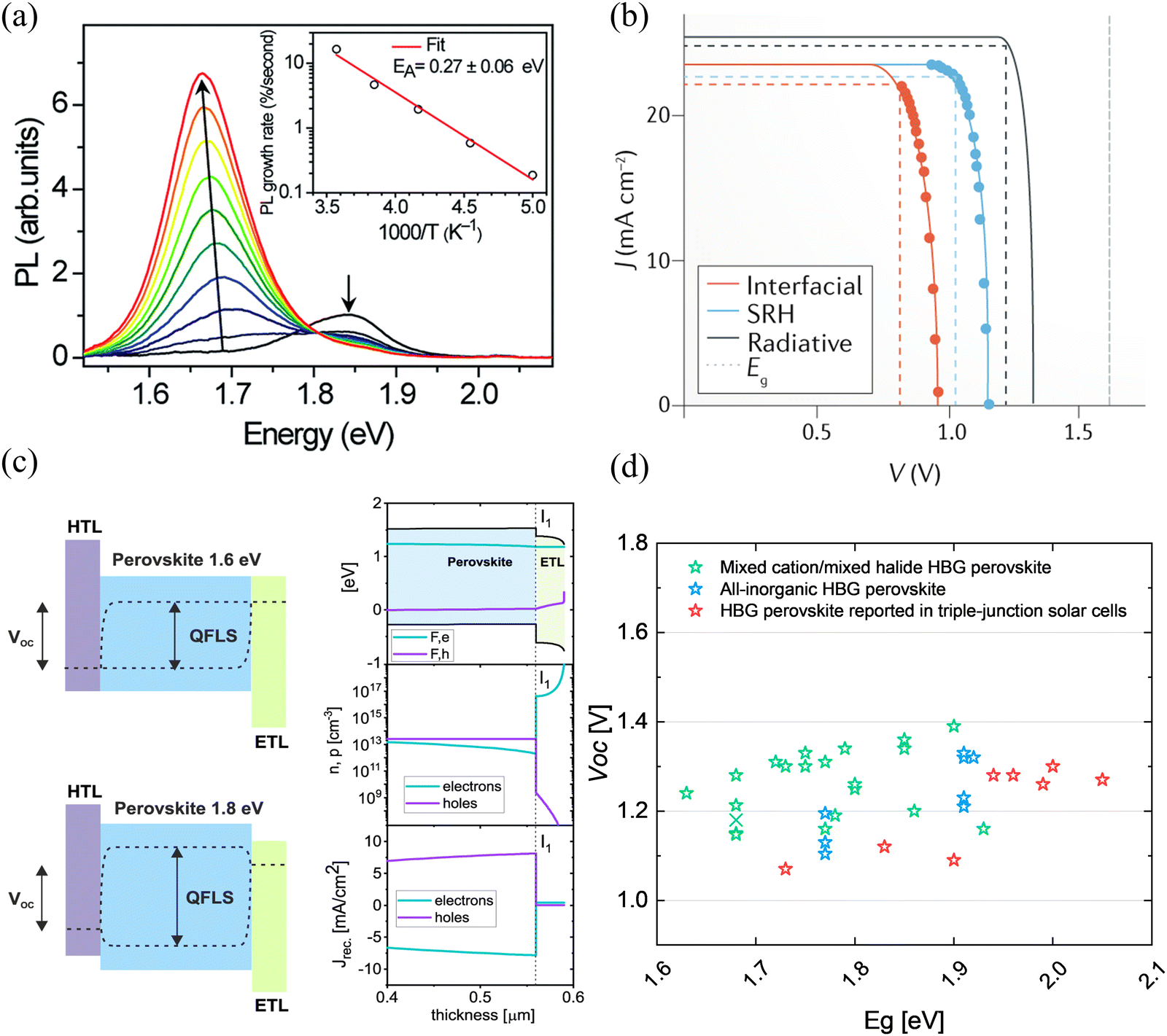 | ||
| Fig. 12 Origin of VOC limitation in HBG perovskite solar cells. (a) Phase segragation of mixed halide high bandgap perovskite. Reproduced from ref. 112 Copyright © 2015, The Royal Society of Chemistry used under a Creative Commons Attribution CC BY 3.0. (b) VOC loss of a solar cell due to non-radiative recombination loss. Reproduced from ref. 115. Copyright © 2020, Springer Nature Limited. (c) Band diagram of peroskite and its charge transport layers showing a band misalignemt for 1.8 eV perovskite due to the fact that the HTL and ETL were optimized for 1.6 eV perovskite. Reproduced from ref. 114 Copyright © 2023, Caprioglio et al. under a Creative Commons Attribution CC BY and (d) VOC of some of the high bandgap perovskite solar cells discussed in this review as a function of the reported bandgaps. The discrapency between VOC and bandgap increases for high bandgap perovskite solar cells. | ||
In order to tackle the above-mentioned issues and improve the VOC in respective compositions several strategies have been reported in literature, which we briefly summarize below.
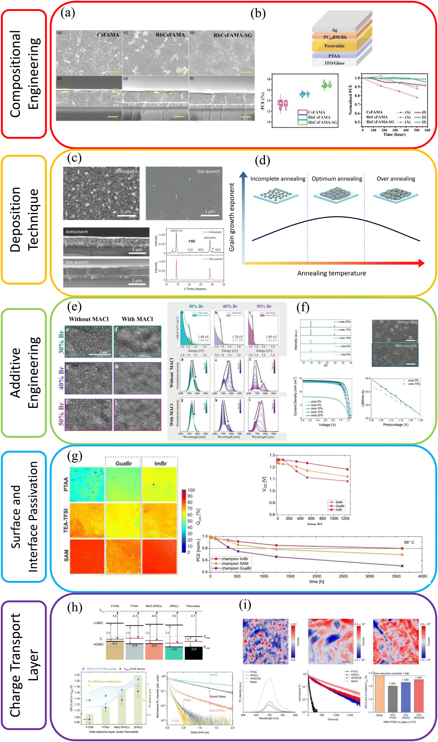
(1) Compositional engineering: the composition of HBG perovskites is an important factor influencing device performance and stability as each composition may induce a different electronic and crystal structure. Therefore, perovskites with same bandgap and different compositions do not necessarily exhibit similar trap states in their films. Bush et al. studied a wide range of double cation (FA/Cs)/double halide (Br/I) perovskite compositions and found that increasing the bandgap should not only be relied on Br content. Increasing the Cs content allows to reduce the Br content (to a certain extend) while maintaining similar bandgap and improving photostability.41 Incorporation of other small cations such as rubidium (Rb)116,117 and potassium (K)118 into the A-site cation of the perovskite composition is another method practiced to slow down phase segregation. This is attributed to increased lattice distortion which introduce a barrier to ion migration.14
(2) Solution preparation and deposition technique: in addition, how the precursor solution is made can have impact on perovskite film quality and consequently its photostability and device efficiency. For example, the standard precursor materials used for preparation of a perovskite solution with double cation composition (e.g., CsxFA1−xPbIyBr1−y) are typically FAI, CsI, PbBr2 and PbI2. Xiao et al. introduced a six precursor system of FAI, CsI, PbBr2 and PbI2, CsBr and FABr for preparation of HBG double cation perovskite (Cs0.2FA0.8PbI1.8Br1.2) and observed experimentally that perovskite solar cells prepared from the six precursor system showed improved photostability compared to the devices made from standard four precursor system.86 The phase segregation phenomenon has also been attributed to defects present at grain boundaries, the bulk or surface of the perovskite that provide channels for ion migration. Therefore, improving the perovskite's bulk quality by increasing the crystallinity and the grain size could lead to enhanced photostability.119 This can be achieved through adaption of the processing method,120 annealing time and annealing temperature.121 Jiang et al. employed a gentle gas quenching method instead of the conventional antisolvent method which resulted in better crystallization of their HBG perovskite and film morphology leading to more than 20.0% PCE for a 1.75 eV perovskite with a high VOC of 1.33 V.120
(3) Additive engineering: additive engineering is another strategy to improve the perovskite's quality as well as passivating the trap states at bulk and grain boundaries. Yu et al. added lead thiocyanate Pb(SCN)2 to their HBG perovskite precursors and achieved much larger grain size compared to their reference perovskite.122 Kim et al. improved the morphology and crystallinity of the HBG perovskite by adding Pb(SCN)2 and phenethylammonium iodide (PEAI) to the perovskite precursor.123 Chloride-based additives such as MACl have also successfully been implemented in HBG perovskite which resulted in more homogeneous halide distribution and mitigation of phase segregation.124–126 Moreover, Thiesbrummel et al. added small amount of oleylamine into HBG perovskite which resulted in improvement of VOC.127 An et al. added phenylethylammonium acetate (PEAAc) additive to a variety of perovskites in the bandgap range of 1.72–1.92 eV. They showed that PEAAc resulted in more homogeneous halide distribution and hence reduced traps.128 Urea as an additive has shown impressive improvement in film quality and performance of 1.96 eV perovskite15 which is discussed further in Section 4.3. It is worth mentioning that the amount of these additives must carefully be tuned with respect to the perovskite composition, bandgap and processing route.119
(4) Interfacial and surface passivation: employing surface and interfacial passivation with materials such as phenylethylammonium iodide (PEAI)129 and butylammonium bromide (BABr),130 which results in formation of a 2D layer on top of 3D perovskite, is an effective method to enable mitigation of halide segregation through passivating defects and blocking ion migration.131 Dual passivation of grain boundaries and surface with 4-fluoro-phenylethylammonium iodide (FPEAI)132 or phenformin hydrochloride are also reported in literature.131 Surface modification of perovskite with electron-donating ligand trioctylphosphine oxide (TOPO) is also reported to reduce the rate of phase segregation.133 Caprioglio et al. introduced a surface passivation between perovskite and PCBM using imidazolium bromide (ImBr) which resulted in growth of a low dimensional perovskite layer on top of perovskite and reduced the voltage loss of 1.80 eV perovskite.114 Similar to additive engineering, successful perovskite surface passivation requires thorough fine tuning of deposition parameters and controlled layer formation optimized for the respective device structure and perovskite composition.
(5) Underlying charge transport layer: proper choice of the charge transport layer can result in enhanced VOC. Up to 2020, PTAA and NiOx were the most widely used HTL of perovskite solar cells in p–i–n configuration, till a group of carbazole-based self-assembled monolayer (SAM) materials, namely 2PACz, MeO-2PACz and Me-4PACz, were introduced.134,135 HBG perovskite devices with SAM exhibited highly improved photostability compared to PTAA.37 Ever since, most of the efficient HBG perovskite solar cells employed SAM in their structure.114,124,127,129,136 Recently, He et al. developed a new SAM (4-(7H-dibenzo[c,g]carbazol-7-yl)butyl)phosphonic acid (4PADCB) as HTL of 1.77 eV perovskite and demonstrated the lowest VOC deficit for such HBG perovskite.137 Currently the HTLs are not specifically optimized for perovskites with bandgap exceeding 1.80 eV, therefore there could be a mismatch between the HTL and perovskite energy levels which needs to be studied and addressed in future.
Fig. 13 summarizes the approaches that has been successfully employed to enhance the performance and stability of HBG perovskite solar cells.
 | ||
| Fig. 13 Approaches reported in literature which successfully suppressed the light-induced phase segregation, non-radiative recombination and energetic band misalignment that improved the VOC and consequently the performance of high bandgap perovskite solar cells. (a) Top view and cross-sectional SEM images of 1.78 eV perovskite films and (b) schematic structure of perovskite solar cell, statistical PCE as well as operational stability over time for perovskite solar cells with and without Rb in the composition. Reproduced with permission from ref. 116. Incorporation of Rb resulted in better film quality, increase in PCE and long term stability. Copyright © 2021 Wiley-VCH GmbH. (c) Top view and cross-sectional SEM images and XRD patterns of 1.75 eV perovskite films deposited using antisolvent and gas quenching methods which shows smooth and dense perovskite film with gas quenching. Reproduced with permission from ref. 120. Copyright © 2022 Jiang et al. some rights reserved; exclusive licensee American Association for the Advancement of Science. (d) Schematic illustration of annealing temperature effect on grain growth of perovskite films. Reproduced with permission from ref. 121. Copyright © 2015, The Royal Society of Chemistry. (e) Top view SEM images and PL measurements over time for perovskite films with bandgap range of 1.68–1.86 eV with and without MACl additive. For HBG perovskite with up to 40% Br, MACl additive improved film quality and consequently suppressed light-induced phase segragation. Reproduced with permission from ref. 126. Copyright © 2023 Wiley-VCH GmbH. (f) XRD patterns, top view SEM images of perovskite films with 1.96 eV bandgap with and withouth urea additive together with jV curve and minority carrier lifetime of the corresponding solar cells. Better crystalinity and film quality for samples with urea additive. Highest PCE is achieved for 15% urea concentration. Reproduced with permission from ref. 15. Copyright © 2023, American Chemical Society. (g) PLQY images of 1.80 eV perovskite passivated with GuaBr and ImBr, VOC over time along with the operational stability of their corresponding solar cells. GuaBr and ImBr passivations, increased the homogeneities and charge collection. Only ImBr passivation resulted in better stability. Reproduced from ref. 114 Copyright © 2023, Caprioglio et al. under a Creative Commons Attribution CC BY. (h) Energetic band alignment, QFLS and transient PL measurements of 1.68 eV perovskite on different HTLs. SAMs as HTL has better energetic alignment with tested perovskite. Higher QFLS and carirer lifetime is achieved for perovskites deposited on SAM compared to PTAA. Reproduced with permission from ref. 135. Copyright © 2019 The Royal Society of Chemistry. (i) PL mapping, PL and transient PL measurements and QFLS of 1.77 eV perovskite with different HTLs. HBG perovskite deposited on 4PADCB showed homogenious PL, longer carrier lifetime, higher PL intensity and consequently QFLS comapred to PTAA and 4PACz. Reproduced with permission from ref. 137. Copyright © 2023, He et al., under exclusive licence to Springer Nature Limited. | ||
4.2 Strategies for stable all-inorganic high bandgap perovskites with bandgaps above 1.77 eV
All-inorganic perovskite compositions with general formula of CsPbX3 are promising to achieve bandgaps above 1.77 eV. They cover a bandgap range of 1.77 eV for CsPbI3 to 2.30 eV for CsPbBr3.40 Although the performances of all-inorganic perovskites still lag behind the standard organic inorganic compositions, they feature better photo-14 as well as thermal stability.138 Until now, the focus of research on all-inorganic perovskites has mostly been on the CsPbI3 composition due to its suitable bandgap for application in dual-junction solar cells. Pure CsPbI3 typically requires high annealing temperature of above 300 °C to form a black phase.138 This becomes challenging in the case of triple-junction solar cells with substrate structure (see Fig. 5) as the high bandgap perovskite is the last solar cell in the deposition order. However, advancement in the field have reduced this high temperature annealing requirement which we explain in this section. In addition, similar to FAPbI3 composition, CsPbI3 experiences phase instability under ambient conditions (at room temperature in presence of moisture) which changes its α-phase to a yellow non-perovskite phase. This is due to the small size of cesium ionic radii that results in non-ideal tolerance factor and structure distortion.139 Recently, the performance of all-inorganic perovskite solar cells has been rapidly improved and a certified PCE of 20.1% was reported for CsPbI3 with a VOC of 1.18 V, FF of 83% and a jSC of 11.5 mA cm−2.140 For CsPbBr3 based solar cells the highest efficiency reported is 11.1%, with an impressive VOC of 1.70 V, a FF of 83% and a jSC of 7.9 mA cm−2.141 However, the bandgaps of all-inorganic single halide perovskites (CsPbI3 with 1.77 eV or CsPbBr3 with 2.30 eV) do not lie within the optimum range of top cell in triple-junction solar cell. Hence, all-inorganic multi halide perovskites CsPbIxBr3−x are more suitable for this purpose.In order to achieve suitable all-inorganic perovskite absorbers at low annealing temperature, and stabilize its phase in ambient condition, several approaches have been reported.
(1) Compositional engineering: incorporation of Br into CsPbI3 lowers the required temperature for crystallization and therefore annealing temperature of CsPbIxBr3−x is lower than that of CsPbI3.138 For example, Beal et al. studied different all-inorganic compositions from pure CsPbBr3 to pure CsPbI3 and reported a structurally stable CsPbI2Br with 1.90 eV bandgap achieved at 135 °C annealing temperature.142 Partial substitution of Cs with Rb can also improve photostability14 as well as moisture stability. For example Cs0.99Rb0.01PbI2Br perovskite remained in black phase after 120 h exposure to ambient air.143 Duan et al. introduced a new precursor system by mixing Cs formate (HCOOCs) with hydrogen lead trihalide (HPbI3 and HPbBr3) powders instead of standard CsI, PbI2, and PbBr2. With this optimized precursor system, they processed CsPbI2Br without any antisolvent step and slowed down the crystallization process. Solar cells based on CsPbI2Br with the new precursor system retained 92% of the original efficiency after more than 800 h storage in ambient air with no encapsulation.144
(2) Solution preparation and deposition technique: Zhu et al. reported that, by aging the perovskite precursor solution up to 3 weeks a pure phase CsPbI2Br film can be achieved at 100 °C annealing temperature.145 Liu et al. processed CsPbI2Br at room temperature by replacing the standard solvent of DMF/DMSO with NMP and combining it with vacuum-assisted extraction of the solvent instead of conventional antisolvent method.146 In addition, samples prepared at room temperature showed prolonged stability against humidity compared to samples prepared with high annealing temperature.146 Mali et al. developed a hot-air assisted method for deposition of CsPbI2Br, in which a hot air gun is used to remove the solvent during spin coating. Employing this method improved the uniformity and crystallinity of black perovskite.147 Chen et al. fabricated CsPbBr3 solar cells by evaporation of CsBr and PbBr2. By optimizing the evaporation rate, high quality films with large grain size were achieved.148 Evaporation of such inorganic high bandgap perovskite shows promising potential for its use as the top cell in a perovskite/perovskite/silicon triple-junction solar cell.
(3) Additive engineering: a stable black CsPbI3 film at 100 °C annealing temperature was reported previously by Eperon et al. by adding small amount of hydroiodic acid (HI) into the perovskite precursor solution.149 Currently HI is the most widely used additive for this type of solar cells.150 Yu Han et al. studied the effect of adding calcium chloride (CaCl2) into CsPbI2Br perovskite and demonstrated that calcium can dope and passivate CsPbI2Br resulting in higher stability in air. Their single-junction perovskite solar cell retained 90% of its initial PCE after more than 1000 h storage in air.151
(4) Interfacial and surface passivation: one of the most important methods to improve moisture-resistance of all-inorganic perovskite is passivation of surface and grain boundaries, which protects the perovskite against moisture penetration. Zhang et al. passivated CsPbIBr2 surface with guanidinium iodide (GuaI) and achieved 9.7% PCE.152 Wang et al. improved moisture-resistance of CsPbI2Br by phenylethyl ammonium chlorine (PEACl) treatment.153 Similarly, post treatment of CsPbI3 with phenyltrimethylammonium bromide (PTABr) resulted in surface passivation of perovskite and improved the stability against humidity. After exposing the perovskite films for 30 minutes to humidity of 80 ± 5% and temperature of 35 °C, the control films turned yellow while the treated samples remained in black phase.154 Very recently Han et al, reported more than 19.0% efficient CsPbI3 perovskite with sequential treatment of the perovskite's surface with ammonium benzenesulfonate (ABS) and phenylethylammonium iodide (PEAI) materials. Samples could retain around 70% of their PCE after 300 h exposure to ambient environment with no encapsulation.155
Fig. 14 summarizes the approaches that have been successfully employed to enhance the stability and performance of all-inorganic HBG perovskite solar cells.
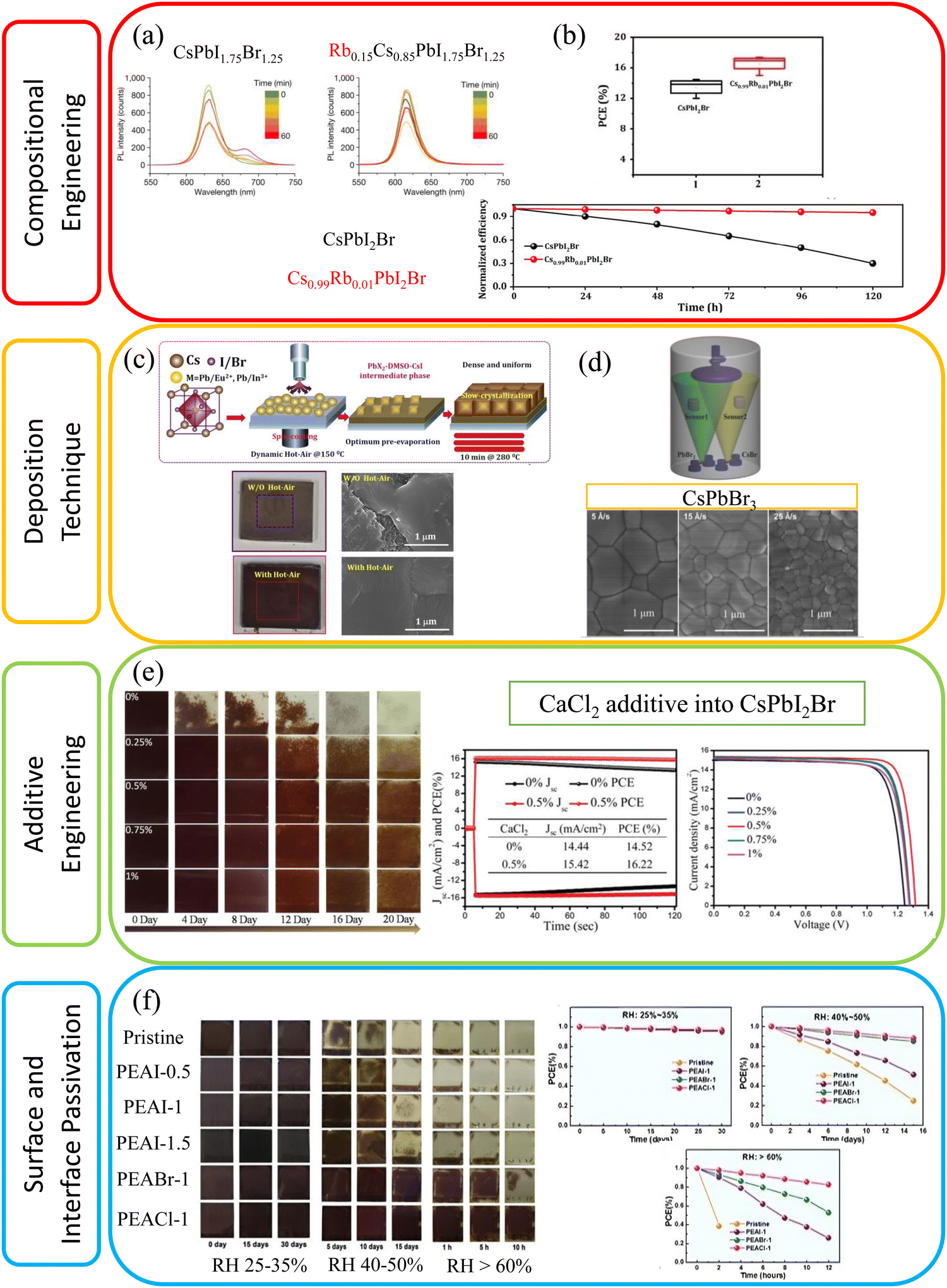 | ||
| Fig. 14 Approaches reported in literature which successfully improved performance and stability of all-inorganic perovskite. (a) PL measurements of CsPbI1.75Br1.25 and Rb0.15Cs0.85PbI1.75Br1.25 perovskites. Reproduced with permission from ref. 14. Copyright © 2023, Wang et al. under exclusive license to Springer Nature Limited. (b) Statistical PCE, stabilized jSC as well as long term stability of the all-inorganic perovskite solar cells with and without Rb in the composition. Better performance, photostability and long-term stability is achieved by incorporation of Rb. Reproduced with permission from ref. 143. Copyright © 2020 WILEY-VCH Verlag GmbH & Co. KGaA, Weinheim. (c) Schematic illustration of dynamic hot-air assisted deposition technique, optical and top view SEM images of CsPbI2Br perovskite processed with and without hot air quenching indicating improved film quality for samples prepared by dynamic hot-air assisted method. Reproduced with permission from ref. 147. Copyright © 2020 Elsevier Inc. (d) Schematic illustration of evaporation deposition of CsPbBr3 and top view SEM images of CsPbBr3 with different evaporation rates. The best film with large grain size is achieved for 5 Å s−1 evaporation rate. Reproduced with permission from ref. 148. Copyright © 2018 WILEY-VCH Verlag GmbH & Co. KGaA, Weinheim. (e) Images of CsPbI2Br films with different amount of CaCl2 additive over time stored at humidity of 40%, together with stabilized jSC and jV curves of the corresponding solar cells. Samples with high CaCl2 concentration are more stable under humidity. Highest PCE is achieved for 0.5% CaCl2 amount. Reproduced with permission from ref. 151. Copyright © 2020 WILEY-VCH Verlag GmbH & Co. KGaA, Weinheim. (f) Images of CsPbI2Br films with different passivation over time stored at humidity range from 25% to more than 60% as well as long-term stability of their corresponding solar cells. Passivated films showed better stability compared to non-passivated films under humidity. Best stability is achieved for PEACl treatment. Reproduced with permission from ref. 153. Copyright © 2018 WILEY-VCH Verlag GmbH & Co. KGaA, Weinheim. | ||
More details on strategies toward improving the PCE and stability of this type of solar cells have been well presented in recent review papers.139,150,156
4.3 High bandgap perovskite top cells in current triple-junction solar cells
On a final note, most of the reported triple-junction solar cells implemented a mixed cation mixed halide composition as top cell absorber. Table 4 summarizes compositions and bandgaps of the top perovskite absorbers in current triple-junction solar cells, as well as device structures and jV performances of respective single-junction solar cells. This section is described in more detail compared to the middle cell absorber as greater focus has been dedicated to suitable high bandgap absorbers for top cell application in triple-junction devices and their development so far.| Year | 2019 | 2020 | 2020 | 2022 | 2022 | 2023 | 2023 | 2023 |
| Composition | FA0.83Cs0.17Pb (Br0.7I0.3)3 | Cs0.1(FA0.66MA0.34)0.9PbI2Br | Cs0.2FA0.8PbI0.9Br2.1 | Cs0.2FA0.8Pb(I0.45Br0.55)3 | Cs0.15MA0.15FA0.70Pb (I0.15Br0.85)3 | Rb0.15Cs0.85PbI1.75Br1.25 | MAPb(I0.5Br0.35Cl0.15)3 | Cs0.05(FA0.55MA0.45)0.95Pb(I0.55Br0.45)3 |
| Bandgap (eV) | 1.94 | 1.73 | 1.99 | 1.90 | 2.05 | 2.00 | 1.96 | 1.83 |
| Structure | Glass/FTO/SnOx/PCBM/perovskite/Spiro-OMeTAD/Ag | Glass/ITO/PTAA/perovskite/C60/BCP/Al | Glass/ITO/PTAA/perovskite/C60/BCP/Cu | Glass/ITO/HTL/perovskite/LiF/C60/BCP/Cu | Glass/ITO/2PACz/perovskite/PhenHCl/C60/BCP/Ag | Glass/ITO/NiOx/Me-4PACz/perovskite/PEAI-EDAI2/PCBM/PEIE/SnOx/Ag | Glass/ITO/Me-4PACz/perovskite/C60/PEIE/Ag | Glass/ITO/2PACz/perovskite/C60/SnOx/Ag/MgF2 |
| Molarity (M) | 0.75 | 0.48 (CsI-PbI2) + 0.095 (FABr-MABr) | 0.80 | 1.00 | 1.10 | 0.80 | 0.75 | 1.20 |
| Thickness (nm) | 350 | 100 | 280 | 180–240 | 100 | 170 | NA | 450 |
| PCE (%) | 11.6 | 8.1 | 10.4 | 9.1 | 8.4 | 13.6 | 13.9 | 11.3 |
| FF (%) | 76.0 | 76.0 | 73.5 | 71.0 | 70.4 | 84.7 | 76.6 | 74.6 |
| j SC (mA cm−2) | 11.9 | 9.9 | 11.2 | 11.7 | 9.4 | 12.4 | 14.16 | 13.6 |
| V OC (V) | 1.28 | 1.07 | 1.26 | 1.09 | 1.27 | 1.30 | 1.28 | 1.12 |
| Top cell in | Pero/pero/pero | Pero/pero/pero | Pero/pero/pero | Pero/pero/silicon | Pero/pero/organic | Pero/pero/pero | Pero/pero/silicon | Pero/pero/silicon |
| Ref. | 23 | 25 | 24 | 17 | 16 | 14 | 15 | 26 |
In the first reported all-perovskite triple-junction solar cell, a FA0.83Cs0.17Pb(Br0.7I0.3)3 perovskite with 1.94 eV bandgap was used. Steps taken to stabilize the high bandgap perovskite were incorporation of 2% potassium (K+) in the precursor to help surpassing ion migration as well as utilizing hydroiodic and hydrobromic acids as additive, which enabled achieving apparent grains in micrometer range. In addition their solution was aged for 2 days prior to the processing.23 As the top cell in the second all-perovskite triple-junction solar cell Wang et al. employed a two-step deposition method for fabrication of their Cs0.1(FA0.66MA0.34)0.9PbI2Br perovskite (1.73 eV).25 Xiao et al. employed Cs0.2FA0.8PbI0.9Br2.1 (1.99 eV) with high bromide content deposited via a one-step antisolvent method. To improve the perovskite quality and increase the grain size, they added 5 mol% Pb(SCN)2 to the perovskite precursor solution.24 For fabrication of fully textured perovskite/perovskite/silicon solar cell, Werner et al. used a 1.80 eV double cation double halide perovskite composition achieved via sequential co-evaporation of PbI2 (layer thickness of 180–200 nm) and CsBr continued by spin coating of FABr solution.22 In the perovskite/perovskite/silicon triple-junction solar cell by Zheng et al. a 1.90 eV perovskite with Cs0.20FA0.80Pb(I0.45Br0.55)3 composition was used. No strategy is reported for stabilizing the high bandgap perovskite in this work.17 The reported perovskite/perovskite/organic triple-junction had a Cs0.15MA0.15FA0.70Pb (I0.15Br0.85)3 perovskite with a ∼2.05 eV bandgap which is the highest bandgap employed in a perovskite-based multi-junction solar cell so far. The perovskite is spin coated from solution with antisolvent method.16 They passivated the top surface of their perovskite layer with phenformin hydrochloride acid, which was previously shown to suppress phase segregation.131 For the first time, Wang et al. used an all-inorganic high bandgap perovskite with Rb0.15Cs0.85PbI1.75Br1.25 composition that has a 2.0 eV bandgap in the record all-perovskite triple-junction solar cell. The stable all-inorganic perovskite was developed by partially replacing Cs with Rb. Incorporation of Rb resulted in increase in lattice distortion that reduced the ion migration and therefore improved photostability under illumination.14 In the record perovskite/perovskite/silicon triple-junction solar cell, a triple halide perovskite composition of MAPb(I0.50Br0.35Cl0.15)3 with 1.96 eV bandgap was employed. Urea was added to the perovskite solution to improve crystallinity and achieve a high-quality perovskite film with large grains without pinholes. Consequently, the performance of the high bandgap perovskite cell significantly improved from 6.4% to 13.9%. The main improvement came from increase in (jSC) in the presence of the urea additive, which they attributed to the enhanced thin-film crystallinity and light absorption.15 We used a Cs0.05(FA0.55MA0.45)0.95Pb(I0.55Br0.45)3 perovskite composition with 1.83 eV bandgap as top cell absorber of perovskite/perovskite/silicon triple-junction cell. A dynamic gas quenching method was used to prevent solvent damage to the already deposited layers. The perovskite film deposited by the adapted method showed homogeneous and compact morphology with improved crystallinity.26
A comprehensive overview on high bandgap perovskite solar cells can be found in the recent review papers.157,158
5. Recombination layer between the perovskite subcells
In monolithic multi-junction solar cells, the subcells are connected in series through recombination layers. The recombination layer has shown to be one of the key factors influencing the performance of tandem solar cells as its electro-optical properties directly affect all photovoltaic parameters (jSC, VOC and FF) of the device.159,160 In a perovskite solar cell, electrons are extracted through an ETL, and holes are extracted through an HTL. In electrically series-connected perovskite subcells without any additional layer, the ETL and HTL of the subcells get in contact. However, there is usually a difference between the work functions of the middle cell's ETL and top cell's HTL.161 Therefore, directly connecting these two layers from different subcells introduce a barrier at this interface160,161 and has shown to result in S-shape jV curves and reduced FF of the device.162 Hence, introducing an additional layer between the subcells with a suitable work function could reduce the mentioned gap and provide recombination sites for the collected charge carriers at HTL and ETL of different subcells. There are several properties that a recombination layer between perovskite subcells must fulfill (Fig. 15) which can be categorized as follows: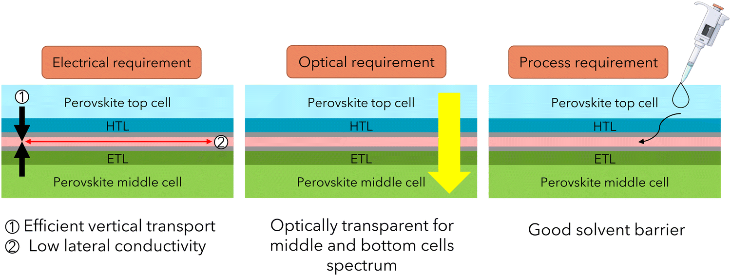 | ||
| Fig. 15 Schematic of relevant electrical, optical and processing requirements for the monolithical connection of perovskite subcells. | ||
1. Electrical requirements
• As the subcells are electrically connected in monolithic multi-junction solar cells, the recombination layer must have low contact resistance.
• It also requires low lateral conductivity to avoid current diffusion.
2. Optical requirements
• The parasitic absorption of this additional layer should be minimum to transmit the light to the underlying subcell. Given the bandgap combinations of the subcells in the dual-junction solar cell, the recombination layer needs to be transmitting especially in the infra-red (IR) range. This spectrum of interest is broader for the recombination layer between the top and middle cell in triple-junction solar cells and is not limited to IR region.
3. Processing requirements
• To avoid possible damages during the processing of the top layers, the recombination layer must protect the layers underneath.
• The processing of the recombination layer itself needs to be compatible in order not to damage the underlying layers.
Generally, there are two common approaches for the recombination layer between the subcells in perovskite-based multi-junction solar cells. Either employing a transparent conductive oxide (TCO) such as sputtered indium tin oxide (ITO) and indium zinc oxide (IZO) or ultrathin metal layer such as gold (Au) and silver (Ag).
A thick layer of sputtered ITO (∼100–120 nm) has been used as recombination layer between the perovskite subcells in early reports on all-perovskite dual-junction solar cells.163,164 In the first proof of concept perovskite/perovskite/silicon triple-junction cell, Werner et al. followed a similar approach and employed 150 nm IZO as the recombination layer between the perovskite middle cell and top cell.22 However, the thick TCO layers have several drawbacks such as low sheet resistance which has shown to result in shunting the solar cells.165 Such thick layers are also optically poor due to high parasitic absorption and possible back reflection.
Most of the recent, highly efficient all-perovskite dual-junction solar cells including the current certified record, employed 1 nm evaporated gold (Au) as recombination layer in their structure.10,120,166 The advantages of evaporated metal layer are its damage-free deposition method compared to sputtering as well as its very high conductivity. However, this layer should be kept as thin as possible (∼1 nm) to minimize parasitic absorption. Later, TCO layers with reduced thickness were employed. Abdollahi Nejand et al. showed that 15 nm of ITO is still optically favorable compared to 1 nm Au, and their all-perovskite dual-junction solar cell exhibited 0.9 mA cm−2 increase in jSC upon replacing Au with ITO as recombination layer.165 We observed similar behavior in our perovskite/perovskite/silicon triple-junction solar cell where the jSC of the device was severely limited by the middle cell. By replacing the Au with an ITO between the perovskite middle cell and top cell, more light was transmitted to middle cell which improved the jSC of the final triple-junction solar cell (Fig. 16f and g).26 Chen et al. developed a recombination layer based on a 4 nm IZO on perovskite/organic tandem solar cell (Fig. 16a and b).162 The perovskite/perovskite/organic triple-junction solar cell also employed only 2 nm IZO as the recombination layer between perovskite middle cell and top cell.16 Palmstrom et al. attempted to produce recombination layer-free all-perovskite dual-junction solar cells. However, based on their results at least 5–15 nm of IZO is needed to achieve high FF.38 Brinkmann et al. demonstrated perovskite/organic dual-junction solar cell with only 1.5 nm indium oxide (InOx) as recombination layer (Fig. 16c–e). Deposition by ALD instead of sputtering enabled formation of such thin and yet conformal InOx layer.129 Commonly, to avoid sputter damage, a buffer layer is deposited prior to sputtering of the TCO layers, which is usually a SnOx layer deposited by ALD. This additional layer also helps to prevent the penetration of solvent during the solution-based processing of the subsequent layers.26 Beyond this, Choi et al. fabricated perovskite/perovskite/silicon triple-junction solar cells without the SnOx buffer layer.15 To enable fabrication of ALD free interconnection layer, Polyethylenimine ethoxylated (PEIE) in methanol was first spin coated on C60 similar to the approach outlined in ref. 14 and 38. Subsequently 20 nm ITO was sputtered on top of the PEIE coated stack. However, to remove the ALD buffer layer, firstly, development of a soft sputtering process is required. Secondly, in the absence of a solvent barrier layer, alternative strategies such as change of the perovskite solvent system15,23 or employing evaporation technique is required for processing of the perovskite layer on top.
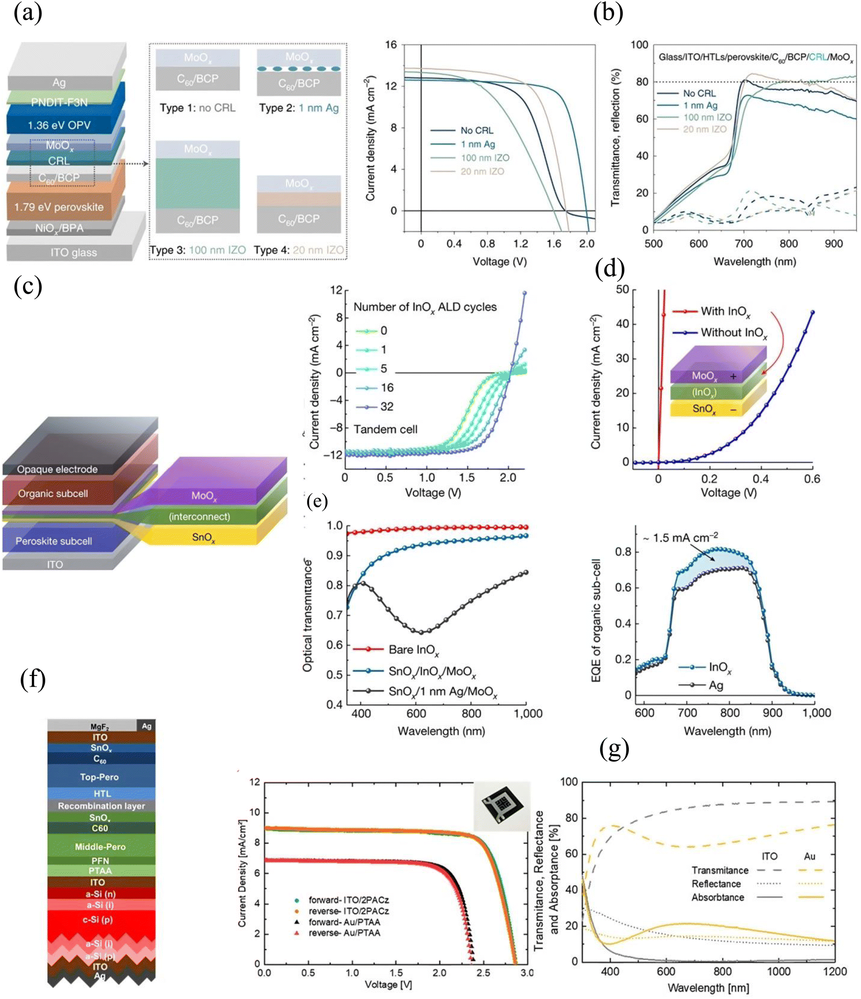 | ||
| Fig. 16 Replacing metal layer with thin TCO as recombination layer. (a) Schematic structure of perovskite/organic dual-junction solar cell with four types of recombination layers and their corresponding jV curves and (b) comparison of transmittance and reflectance of the tested recombination layers. Reproduced with permission from ref. 162. Copyright © 2022, Springer Nature. (c) Schematic structure of perovskite/organic dual-junction solar cell with different thicknesses of ALD deposited InOx as recombination layer and their corresponding jV curves. (d) Diode characteristic of (SnOx)/(InOx)/(MoOx). (e) Comparison of transmittance of ∼1.5 nm of InOx and 1 nm Ag, and EQE of the organic bototm cell with 1.5 nm of InOx and 1 nm Ag as recombination layer. Reproduced with permission from ref. 129 Copyright © 2022, Springer Nature. (f) Schematic structure of perovskite/perovskite/silicon triple-junction solar cell with Au/PTAA and ITO/2PACz as interconnection layers and their corresponding jV curves and (g) comparison of transmittance, reflectance and absorptance of the 1 nm of Au with 15 nm of ITO. Reproduced with permission from ref. 26 Copyright © 2023 Heydarian et al., Published by American Chemical Society. Under a Creative Commons Attribution CC-BY-NC-ND 4.0. All examples indicate improved optical properties of the recombination layer upon replacing the metal layer with thin TCO. Improved electrical property is achieved by optimizing the thickness of the TCO layer. | ||
Recently, a 23.7% efficient all-perovskite dual-junction solar cell with no TCO or metal based recombination layer was reported by directly contacting the SnOx buffer layer and the HTL (PEDOT:PSS) of the low bandgap perovskite.167 Even though this work highlights the potential of a simplified recombination layer, further study is needed to assess the possible formation of a Schottky barrier when the SnOx and other HTL materials get in contact. Future work should focus on developing an ideal recombination layer between the subcells in multi-junction solar cells. In addition to the high parasitic absorption, taking the production cost into account, gold is the least favorable material to be used and material availability of both gold and indium are critical. Another motivation to avoid using a metal layer, especially in the substrate configuration (Fig. 5) where HBG perovskite is processed on top of the recombination layer, is that the common self-assembled monolayer (SAM) hole transport materials for HBG perovskites (see Section 4) cannot directly be deposited on metal as they require hydroxyl (–OH) groups to bind to in a condensation reaction.168 In that respect the surface of the recombination layer should provide sufficient –OH groups to ensure homogeneous coverage of SAM.
Research on alternative indium-free recombination layers such as aluminum-doped zinc oxide (AZO) is ongoing. For example zinc oxide (ZnO)/AZO has been used as recombination layer in copper indium selenium (CuInSe2)/perovskite dual-junction solar cell.169 AZO has also been employed as front contact of SHJ solar cells170 which opens up the window for replacing the common TCO recombination layer between silicon and perovskite subcells. In addition, according to Messmer et al. the final cost of the solar cell significantly drops by replacing ITO layer with AZO.171
Finally, it is important to mention that optimizing the recombination layer between two subcells in a triple-junction solar cell is complex as one cannot evaluate the quality of the recombination layer independent from the effect of the connection to the third subcell.
6. Characterization of triple-junction solar cells
Precise characterization of solar cells is highly important in research and development. Solar cell's performance data reported in literature are mainly from in-house measurements. While for single-junction solar cells the measurement approach and interpretation of data is more straightforward, a sophisticated procedure is needed for multi-junction solar cells, especially in two-terminal structures where no direct electrical access to the individual subcells is possible and additional effects such as luminescent coupling can occur for current mismatched subcells. This gets more challenging by adding to the number of junctions. Even though perovskite-based triple-junction solar cells are at the early stage of development, there is extensive research and well-established measurement standards for multi-junction solar cells based on III–V materials,172–177 from which the perovskite community can benefit.6.1 External quantum efficiency (EQE) measurement
The general method for correct EQE measurement of monolithically series-connected solar cells has been first presented by Burdick and Glatfelter in 1986 for a-Si/Si dual-junction solar cells178 and was extended for a GaInP/GaInAs/Ge triple-junction solar cell by Meusel et al.173 The method is used to characterize multi-junction devices independent of their material. In summary, the EQE of each subcell in a two-terminal triple-junction solar cell can be measured individually provided that the subcell of interest limits the overall current. To achieve this, the solar cell is illuminated with spectrally selective bias lights to saturate the other subcells so that they generate larger photocurrents than the subcell under test. The suitable selective bias light depends on the spectral responses of the subcells and can be provided by wavelength specific bias lights such as LEDs or the use of optical filters in combination with broadband light sources.179 In addition, to determine the EQE correctly, the subcell under test needs to operate at its short-circuit condition, therefore an external voltage equal to the sum of the voltages of the other two subcells under the bias light condition needs to be applied. Estimating the appropriate bias voltage value requires further effort as the exact values of the subcell voltages at this low irradiance are often not known and in this case the procedure described in International Electrotechnical Commission (IEC) should be followed.179One common challenge in EQE measurement of multi-junction solar cells are measurement artifacts.174,175 Subcell properties (e.g., low parallel resistance (Rp), early reverse breakdown and high radiative recombination) in combination with non-correct measurement settings (bias voltage, spectrally tuned bias light) can cause interaction between them during measurement which introduce undesired measurement artifacts such that the EQE of other subcells appears in the measured EQE-data of the subcell of interest. At the same time the absolute EQE of the measured subcell is lower than expected. This effect usually happens when the solar cells have low parallel resistance or low breakdown voltages leading to a change in operating voltage during measurement.173 In addition, the luminescence coupling is another source of artifact in EQE measurement of multi-junction solar cells.176,180 However, EQE measurement of perovskite-based multi-junction solar cells with artifacts caused by luminescent coupling has not been reported yet. Therefore, in the following we will focus on artifacts caused by low parallel resistance or low breakdown voltage. This is one of the major challenges associated with EQE measurement of multi-junction solar cells that is widely discussed for III–V based multi-junction solar cells (Fig. 17a).173 The measurement artifact can be corrected mathematically as described in ref. 174 and 175. However, it has been shown by Reichmuth et al. that the typical correction procedure based on the assumption of a uniform Rp might lead to deviations from the true EQE.181 These lateral effects may become more relevant for industrial-size solar cells.
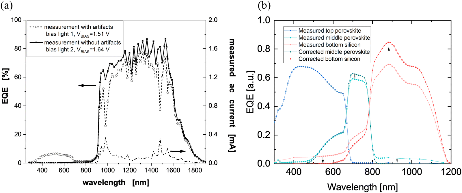 | ||
| Fig. 17 (a) Measurement artifact at spectral response (SR) range of top cell during EQE measurements of the germanium (Ge) bottom cell of a III–V/III–V/Ge triple-junction solar cell. With permission from ref. 173 Copyright © 2003 John Wiley & Sons, Ltd. (b) EQE curves of a perovskite/perovskite/silicon triple-junction solar cell measured at Fraunhofer ISE CalLab. Artifacts are visible for both middle cell and bottom cell EQEs. The EQE measurements with artifacts and the corrected curves are presented. | ||
For the case of perovskite/perovskite/silicon triple-junction solar cells, we have observed this effect in our lab when measuring the EQE of a silicon bottom cell in which the artifact in the spectral response range of the top and middle cells (300–750 nm) is visible (Fig. 17b) and also the as-measured EQE curve of the middle cell shows an artifact in the spectral response range of the bottom cell (800–1200 nm) (Fig. 17b). The artifacts have been corrected with the method described in ref. 174. In summary, for the case of middle cell, a scaling factor (S) is determined to bring the EQE of the bottom cell to the level of the artifact at 800–1200 nm. Then the scaled curve is subtracted from the measured EQE to remove the artifact. Additionally, the measured EQE up to 800 nm is divided by (1 − S). Similar procedure is applied to correct the EQE of the bottom cell.
Apart from the common challenges described above, several other factors and measurement conditions are shown to have an impact on the absolute EQE of perovskite solar cells due to their dynamic effects.182 Mundus et al. investigated the non-linearity of various single-junction perovskite solar cells and showed that the jSC has non-linear behavior with respect to the irradiance leading to a dependency of the EQE on bias illumination intensity.183,184 Mercaldo et al. reported similar effect.184 Other parameters such as chopper wheel frequency,184–188 preconditioning of the cell187 and applied bias voltage are also reported to affect the absolute EQE.187 Also, the common approach to measure the EQE with a monochromatic beam smaller than the active area of the solar cell can cause deviations in the signal compared to when illuminating the whole area including all metallization, the edges and spatially different absorber thickness, radiative properties etc.181 Therefore, calculating the generated current from measured EQE data obtained for individual subcells is not straightforward. Consequently, determining the current matching situation of the perovskite-based multi-junction solar cells from EQE measurement can result in misinterpretation.189 An alternative approach based on spectrometric characterization for precise determination of current matching could in the future be used for perovskite-based triple-junction solar cells.172 This approach has been successfully applied on perovskite/silicon dual-junction solar cells.189
6.2 Current density–voltage (jV) measurement
Accurate jV measurement of multi-junction solar cells require a different procedure than that necessary for the characterization of single-junction solar cells. In the case of single-junction solar cells, the difference between the AM 1.5g reference spectrum and the simulator spectrum can be calculated with the mismatch factor and the intensity (often of a single broad band lamp) is set for the specific solar cell under test. For multi-junction solar cells however, the simple intensity variation of a single lamp will for most cases not reach AM 1.5g reference conditions within all subcells. Although a solar simulator might be classified to have a closely matched spectrum, even small spectral differences will lead to incorrect subcell currents. Therefore, also the relative spectral irradiance of the solar simulator needs to be tuned based on the spectral response of each solar cell individually (usually with multiple light-sources).172,190For multi-junction solar cells, the solar simulator spectrum needs to generate the same current in each subcell as under the reference spectrum (normally the AM 1.5g spectrum). That means, in case of triple-junction solar cells the following equation system must be fulfilled:
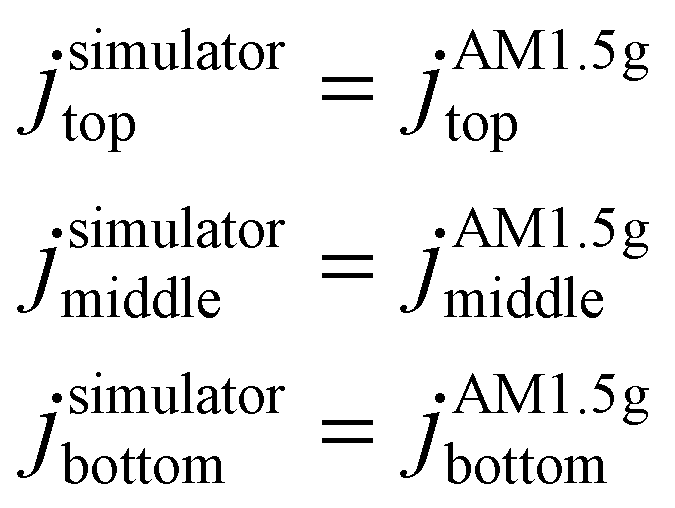
Since research on triple-junction solar cells is at an early stage, following the IEC measurement procedure for measurements in the research labs is necessary for comparison between reported data and therefore increase the reliability of this emerging photovoltaic technology.
Here we summarize the measurement protocol of Fraunhofer ISE CalLab using three light source solar simulator:
I. SR measurement of the individual subcells.
II. Solving the following equation system based on the discussed conditions.
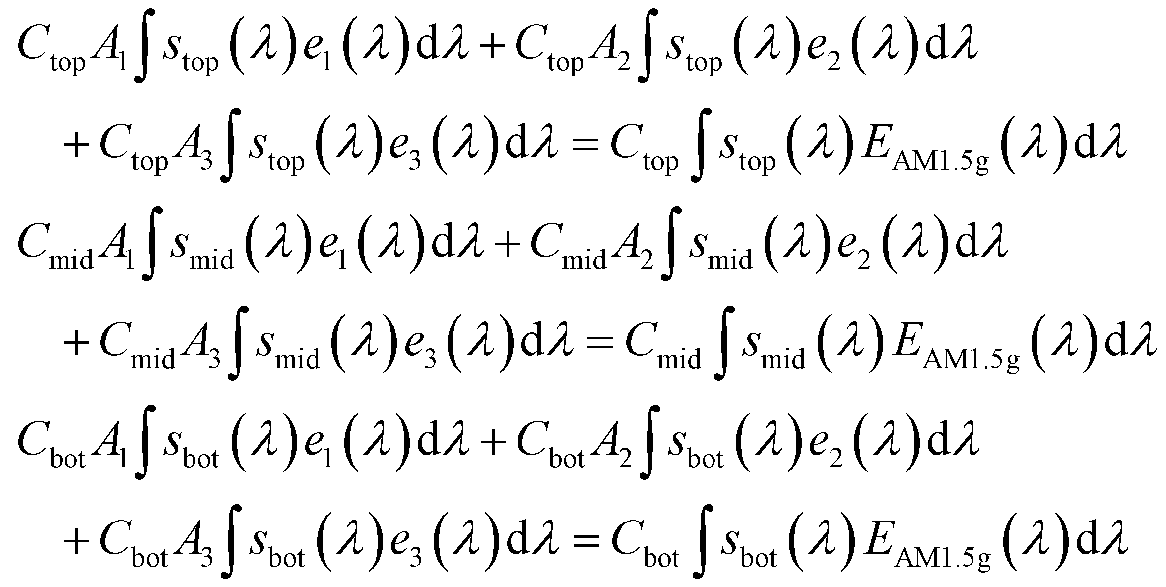
III. In case of measuring perovskite-based solar cells, measurements should be performed in forward and reverse scan directions.
IV. Reporting stabilized PCE determined from fixed voltage or maximum power point (MPP) tracking.
7. Summary and outlook
While the highly efficient perovskite-based dual-junction solar cells especially on silicon bottom cells have already shown to be an attractive option for further efficiency improvement of future PV modules, perovskite-based triple-junction solar cells have the potential to surpass the efficiency limit of dual-junction solar cells. So far, the perovskite community has mostly focused on the optimization of single and dual-junction solar cells and limited effort has been spent on development of triple-junction solar cells using perovskite semiconductors. Therefore, the PCE achieved for triple-junction solar cells is limited to 22.2%, 23.3%, and 19.4% on a silicon, perovskite, and organic bottom cell, respectively, well below their theoretical potential. We believe that the focus is now changing, and it is only a matter of time until the triple-junction solar cell development undergoes a fast efficiency increase similar to the trend of perovskite/silicon tandem solar cells or even faster as the learnings from single- and dual-junction can be transferred to triple-junction solar cells. In this review we summarized the recent advancements of perovskite-based triple-junction solar cells, their theoretical potential, and their challenges. Based on what has been discussed we identify the main losses and important topics for future work.Regarding the VOC, according to simulations,27 a practical VOC of 3.54 V for all-perovskite and 3.24 V for perovskite/perovskite/silicon triple-junction solar cells can be achieved, respectively. So far, the maximum VOC values realized for these two types of solar cells are limited to 3.20 V for all-perovskite and 2.87 V for perovskite/perovskite/silicon triple-junction cells. Analyzing the VOC values reported in the subcells of these two configurations, for middle bandgap single-junction cells, the VOC deficit ranges from 0.40 V to 0.54 V, while for high bandgap cells, it is between 0.66 V and 0.81 V. Given the higher VOC deficit in high bandgap perovskite subcells, there is a need for strategies to develop efficient and stable high bandgap perovskite in the optimum range of 1.85–2.15 eV with high voltage output. For this purpose, the high bandgap perovskite needs excellent material quality, which can be achieved by careful compositional engineering, additive engineering, processing control, surface treatment and interfacial passivation. In addition, so far even with the latest progress in the field, which resulted in high bandgap perovskite with satisfactory efficiency, the stability of such perovskite is not fully addressed. In terms of charge transport layer materials, the work function and band alignment of conventional materials with regard to adapted bandgap perovskites have not been fully studied and there has been little adjustment to the respective valence and conduction band levels. More work needs to be done on this topic, as it could bear a big leverage for VOC improvement.
In addition, development of a lossless recombination layer between the middle perovskite and high bandgap perovskite with proper barrier function is a relatively new research field but critical for process compatibility and high voltage output.
In terms of jSC, a practical maximum jSC of 12.0 mA cm−2 and 14.1 mA cm−2 can be achieved for all-perovskite and perovskite/perovskite/silicon triple-junction solar cells, respectively.27 However, the maximum jSC reported for these two structures are still lower than expected with 9.6 mA cm−2 for all-perovskite and 10.2 mA cm−2 for perovskite/perovskite/silicon triple-junction solar cells. There are two main origins for this jSC limitation. Firstly, triple-junction solar cells consist of many interlayers, which introduce parasitic absorption leading to lower jSC of the final device. In order to maximize the jSC, materials with high transparency need to be employed as electrodes, recombination and charge transport layers. In addition, the thickness of all layers except for the absorber layers should be optimized to introduce minimum parasitic absorption. Secondly, current matching has not been achieved for most of the reported triple-junction solar cells. Even though proper evaluation of current matching condition requires further effort, it is clear that current perovskite/perovskite/silicon solar cells are using non-optimum bandgap combinations and have a current limitation caused by the middle cell. Up to now, bandgaps employed for the middle cell of this structure are in the range of 1.50–1.60 eV. By lowering the bandgap of the perovskite middle cell (employing FAPbI3 or Sn-containing perovskite), a better current matching could be achieved in the final device.
In addition to what has been mentioned, depending on the technology, further development and adaptation is necessary.
• Perovskite/perovskite/silicon
Since the high bandgap perovskite cell is the last subcell processed in this structure, not only suitable bandgap with good stability is required, but also a deposition technique must be employed with no damage to the underlying layers. This adds to the challenges of high bandgap perovskite development. In this regard, fully evaporated high bandgap perovskite could be the next focus, as apart from the process compatibility, it has several other advantages e.g., in terms of upscaling.
• Perovskite/perovskite/perovskite
Development of a stable low bandgap perovskite in this structure is of great importance. Moreover, since the low bandgap perovskite is processed in the last step, it requires a deposition technique that introduces no damage to the two-underlying perovskite subcells. Therefore, all-perovskite multi-junction solar cells could highly benefit from development of efficient and stable evaporated Sn-based perovskite.
• Perovskite/perovskite/organic
So far, efficient organic solar cells have mostly been realized with a bandgap of 1.30 eV. Employing the organic solar cell as the low bandgap subcell in triple-junction solar cells requires further reduction of its bandgap.
Finally, it is worth mentioning that precise characterization in parallel to the development of triple-junction solar cells is crucial to increase the reliability of the measurements and get better insight into the limitation of this new technology. For comparable jV measurements, it is especially important to correctly adjust the spectrum of the solar simulator in a way that all subcells generate the same current as they would do under the reference spectrum. Furthermore, along with PCE enhancement, stability and scalability of perovskite-based solar cells need to be addressed for future commercialization of this technology. With regards to the triple-junction solar cells, so far, the focus has been on improving the efficiency, while the stability of the reported solar cells is less studied.
Author contributions
M. Heydarian and M. Heydarian (conceptualization, data curation, formal analysis, visualization, writing – original draft, writing – review & editing), P. Schygulla (data curation, formal analysis, visualization; writing – review & editing), S. K. Reichmuth (data curation, formal analysis, visualization, writing – review & editing), A. J. Bett (formal analysis, writing – review & editing), J. Hohl-Ebinger (project administration, supervision), F. Schindler (funding acquisition, project administration, supervision, writing – review & editing), M. Hermle (funding acquisition, project administration, supervision), M. C. Schubert (funding acquisition, project administration, supervision, writing – review & editing), P. S. C. Schulze (conceptualization, formal analysis, writing – review & editing, supervision), J. Borchert (conceptualization, funding acquisition, project administration, supervision, writing – review & editing), S. W. Glunz (conceptualization, funding acquisition, supervision, writing – review & editing).Conflicts of interest
The authors declare no competing financial interest.Acknowledgements
This work was partially supported by the European Union through the Horizon Europe project Triumph under the number 101075725 and the German Federal Ministry for Economic Affairs and Climate Action (BMWK) under contract number 03EE1132A (RIESEN).References
- S. P. Philipps and A. W. Bett, III–V Multi-junction solar cells and concentrating photovoltaic (CPV) systems, Adv. Opt. Technol., 2014, 3, 33, DOI:10.1515/aot-2014-0051.
- R. M. France, J. F. Geisz, T. Song, W. Olavarria, M. Young, A. Kibbler and M. A. Steiner, Triple-junction solar cells with 39.5% terrestrial and 34.2% space efficiency enabled by thick quantum well superlattices, Joule, 2022, 6, 1121–1135, DOI:10.1016/j.joule.2022.04.024.
- K. Derendorf, S. Essig, E. Oliva, V. Klinger, T. Roesener, S. P. Philipps, J. Benick, M. Hermle, M. Schachtner, G. Siefer, W. Jager and F. Dimroth, Fabrication of GaInP/GaAs//Si Solar Cells by Surface Activated Direct Wafer Bonding, IEEE J. Photovoltaics, 2013, 3, 1423–1428, DOI:10.1109/jphotov.2013.2273097.
- P. Schygulla, R. Müller, D. Lackner, O. Höhn, H. Hauser, B. Bläsi, F. Predan, J. Benick, M. Hermle, S. W. Glunz and F. Dimroth, Two-terminal III–V//Si triple-junction solar cell with power conversion efficiency of 35.9% at AM 1.5g, Prog. Photovoltaics, 2022, 30, 869–879, DOI:10.1002/pip.3503.
- L. Vauche, E. Veinberg-Vidal, C. Weick, C. Morales, V. Larrey, C. Lecouvey, M. Martin, J. Da Fonseca, C. Jany, T. Desrues, C. Brughera, P. Voarino, T. Salvetat, F. Fournel, M. Baudrit and C. Dupre, Wafer bonding approaches for III–V on Si multi-junction solar cells, in 2017 IEEE 44th Photovoltaic Specialist Conference (PVSC), IEEE, Washington, DC, 2017, pp. 2492–2497 Search PubMed.
- M. Feifel, D. Lackner, J. Schön, J. Ohlmann, J. Benick, G. Siefer, F. Predan, M. Hermle and F. Dimroth, Epitaxial GaInP/GaAs/Si Triple-Junction Solar Cell with 25.9% AM 1.5g Efficiency Enabled by Transparent Metamorphic AlxGa1−xAsyP1−y Step-Graded Buffer Structures, Sol. RRL, 2021, 2000763, DOI:10.1002/solr.202000763.
- M. A. Green, A. Ho-Baillie and H. J. Snaith, The emergence of perovskite solar cells, Nat. Photonics, 2014, 8, 506–514, DOI:10.1038/nphoton.2014.134.
- S. D. Stranks, G. E. Eperon, G. Grancini, C. Menelaou, M. J. P. Alcocer, T. Leijtens, L. M. Herz, A. Petrozza and H. J. Snaith, Electron-hole diffusion lengths exceeding 1 micrometer in an organometal trihalide perovskite absorber, Science, 2013, 342, 341–344, DOI:10.1126/science.1243982.
- C. S. Ponseca, T. J. Savenije, M. Abdellah, K. Zheng, A. Yartsev, T. Pascher, T. Harlang, P. Chabera, T. Pullerits, A. Stepanov, J.-P. Wolf and V. Sundström, Organometal halide perovskite solar cell materials rationalized: ultrafast charge generation, high and microsecond-long balanced mobilities, and slow recombination, J. Am. Chem. Soc., 2014, 136, 5189–5192, DOI:10.1021/ja412583t.
- R. Lin, Y. Wang, Q. Lu, B. Tang, J. Li, H. Gao, Y. Gao, H. Li, C. Ding, J. Wen, P. Wu, C. Liu, S. Zhao, K. Xiao, Z. Liu, C. Ma, Y. Deng, L. Li, F. Fan and H. Tan, All-perovskite tandem solar cells with 3D/3D bilayer perovskite heterojunction, Nature, 2023, 620, 994–1000, DOI:10.1038/s41586-023-06278-z#.
- M. Jošt, E. Köhnen, A. Al-Ashouri, T. Bertram, Š. Tomšič, A. Magomedov, E. Kasparavicius, T. Kodalle, B. Lipovšek, V. Getautis, R. Schlatmann, C. A. Kaufmann, S. Albrecht and M. Topič, Perovskite/CIGS Tandem Solar Cells: From Certified 24.2% toward 30% and Beyond, ACS Energy Lett., 2022, 7, 1298–1307, DOI:10.1021/acsenergylett.2c00274.
- X. Wang, D. Zhang, B. Liu, X. Wu, X. Jiang, S. Zhang, Y. Wang, D. Gao, L. Wang, H. Wang, Z. Huang, X. Xie, T. Chen, Z. Xiao, Q. He, S. Xiao, Z. Zhu and S. Yang, Highly Efficient Perovskite/Organic Tandem Solar Cells Enabled by Mixed-Cation Surface Modulation, Adv. Mater., 2023, e2305946, DOI:10.1002/adma.202305946.
- NREL, Best Research-Cell Efficiencies, https://www.nrel.gov/pv/cell-efficiency.html (accessed: October 2023).
- Z. Wang, L. Zeng, T. Zhu, H. Chen, B. Chen, D. J. Kubicki, A. Balvanz, C. Li, A. Maxwell, E. Ugur, R. Dos Reis, M. Cheng, G. Yang, B. Subedi, D. Luo, J. Hu, J. Wang, S. Teale, S. Mahesh, S. Wang, S. Hu, E. Jung, M. Wei, S. M. Park, L. Grater, E. Aydin, Z. Song, N. J. Podraza, Z.-H. Lu, J. Huang, V. P. Dravid, S. de Wolf, Y. Yan, M. Grätzel, M. Kanatzidis and E. Sargent, Suppressed phase segregation for triple-junction perovskite solar cells, Nature, 2023, 618, 74–79, DOI:10.1038/s41586-023-06006-7.
- Y. J. Choi, S. Y. Lim, J. H. Park, S. G. Ji and J. Y. Kim, Atomic Layer Deposition-Free Monolithic Perovskite/Perovskite/Silicon Triple-Junction Solar Cells, ACS Energy Lett., 2023, 8, 3141–3146, DOI:10.1021/acsenergylett.3c00919.
- F. H. Isikgor, T. Maksudov, X. Chang, B. Adilbekova, Z. Ling, W. T. Hadmojo, Y. Lin and T. D. Anthopoulos, Monolithic Perovskite–Perovskite–Organic Triple-Junction Solar Cells with a Voltage Output Exceeding 3 V, ACS Energy Lett., 2022, 7, 4469–4471, DOI:10.1021/acsenergylett.2c02340.
- J. Zheng, G. Wang, W. Duan, M. A. Mahmud, H. Yi, C. Xu, A. Lambertz, S. Bremner, K. Ding, S. Huang and A. W. Y. Ho-Baillie, Monolithic Perovskite–Perovskite–Silicon Triple-Junction Tandem Solar Cell with an Efficiency of over 20%, ACS Energy Lett., 2022, 7, 3003–3005, DOI:10.1021/acsenergylett.2c01556.
- M. Feifel, D. Lackner, J. Ohlmann, J. Benick, M. Hermle and F. Dimroth, Direct Growth of a GaInP/GaAs/Si Triple-Junction Solar Cell with 22.3% AM 1.5g Efficiency, Sol. RRL, 2019, 1900313, DOI:10.1002/solr.201900313.
- M. Feifel, J. Ohlmann, J. Benick, M. Hermle, J. Belz, A. Beyer, K. Volz, T. Hannappel, A. W. Bett, D. Lackner and F. Dimroth, Direct Growth of III–V/Silicon Triple-Junction Solar Cells With 19.7% Efficiency, IEEE J. Photovoltaics, 2018, 8, 1590–1595, DOI:10.1109/JPHOTOV.2018.2868015.
- R. Cariou, J. Benick, F. Feldmann, O. Höhn, H. Hauser, P. Beutel, N. Razek, M. Wimplinger, B. Bläsi, D. Lackner, M. Hermle, G. Siefer, S. W. Glunz, A. W. Bett and F. Dimroth, III–V-on-silicon solar cells reaching 33% photoconversion efficiency in two-terminal configuration, Nat. Energy, 2018, 3, 326–333, DOI:10.1038/s41560-018-0125-0.
- D. Lackner, O. Höhn, R. Müller, P. Beutel, P. Schygulla, H. Hauser, F. Predan, G. Siefer, M. Schachtner, J. Schön, J. Benick, M. Hermle and F. Dimroth, Two-Terminal Direct Wafer-Bonded GaInP/AlGaAs//Si Triple-Junction Solar Cell with AM 1.5g Efficiency of 34.1%, Sol. RRL, 2020, 2000210, DOI:10.1002/solr.202000210.
- J. Werner, F. Sahli, F. Fu, J. J. Diaz Leon, A. Walter, B. A. Kamino, B. Niesen, S. Nicolay, Q. Jeangros and C. Ballif, Perovskite/Perovskite/Silicon Monolithic Triple-Junction Solar Cells with a Fully Textured Design, ACS Energy Lett., 2018, 3, 2052–2058, DOI:10.1021/acsenergylett.8b01165.
- D. P. McMeekin, S. Mahesh, N. K. Noel, M. T. Klug, J. Lim, J. H. Warby, J. M. Ball, L. M. Herz, M. B. Johnston and H. J. Snaith, Solution-Processed All-Perovskite Multi-junction Solar Cells, Joule, 2019, 3, 387–401, DOI:10.1016/j.joule.2019.01.007.
- K. Xiao, J. Wen, Q. Han, R. Lin, Y. Gao, S. Gu, Y. Zang, Y. Nie, J. Zhu, J. Xu and H. Tan, Solution-Processed Monolithic All-Perovskite Triple-Junction Solar Cells with Efficiency Exceeding 20%, ACS Energy Lett., 2020, 5, 2819–2826, DOI:10.1021/acsenergylett.0c01184.
- J. Wang, V. Zardetto, K. Datta, D. Zhang, M. M. Wienk and R. A. Janssen, 16.8% Monolithic all-perovskite triple-junction solar cells via a universal two-step solution process, Nat. Commun., 2020, 11, 5254, DOI:10.1038/s41467-020-19062-8.
- M. Heydarian, M. Heydarian, A. J. Bett, M. Bivour, F. Schindler, M. Hermle, M. C. Schubert, P. S. C. Schulze, J. Borchert and S. W. Glunz, Monolithic Two-Terminal Perovskite/Perovskite/Silicon Triple-Junction Solar Cells with Open Circuit Voltage >2.8 V, ACS Energy Lett., 2023, 8, 4186–4192, DOI:10.1021/acsenergylett.3c01391.
- M. T. Hörantner, T. Leijtens, M. E. Ziffer, G. E. Eperon, M. G. Christoforo, M. D. McGehee and H. J. Snaith, The Potential of Multijunction Perovskite Solar Cells, ACS Energy Lett., 2017, 2, 2506–2513, DOI:10.1021/acsenergylett.7b00647.
- L. Zhu, T. Mochizuki, M. Yoshita, S. Chen, C. Kim, H. Akiyama and Y. Kanemitsu, Conversion efficiency limits and bandgap designs for multi-junction solar cells with internal radiative efficiencies below unity, Opt. Express, 2016, 24, A740–51, DOI:10.1364/OE.24.00A740.
- W. Guter, J. Schöne, S. P. Philipps, M. Steiner, G. Siefer, A. Wekkeli, E. Welser, E. Oliva, A. W. Bett and F. Dimroth, Current-matched triple-junction solar cell reaching 41.1% conversion efficiency under concentrated sunlight, Appl. Phys. Lett., 2009, 94, 223504 CrossRef.
- E. Aydin, T. G. Allen, M. de Bastiani, L. Xu, J. Ávila, M. Salvador, E. van Kerschaver and S. de Wolf, Interplay between temperature and bandgap energies on the outdoor performance of perovskite/silicon tandem solar cells, Nat. Energy, 2020, 5, 851–859, DOI:10.1038/s41560-020-00687-4.
- M. de Bastiani, A. J. Mirabelli, Y. Hou, F. Gota, E. Aydin, T. G. Allen, J. Troughton, A. S. Subbiah, F. H. Isikgor, J. Liu, L. Xu, B. Chen, E. van Kerschaver, D. Baran, B. Fraboni, M. F. Salvador, U. W. Paetzold, E. H. Sargent and S. de Wolf, Efficient bifacial monolithic perovskite/silicon tandem solar cells via bandgap engineering, Nat. Energy, 2021, 6, 167–175, DOI:10.1038/s41560-020-00756-8.
- M. Babics, H. Bristow, A. R. Pininti, T. G. Allen and S. de Wolf, Temperature coefficients of perovskite/silicon tandem solar cells, ACS Energy Lett., 2023, 3013–3015, DOI:10.1021/acsenergylett.3c00930.
- J. P. Mailoa, C. D. Bailie, E. C. Johlin, E. T. Hoke, A. J. Akey, W. H. Nguyen, M. D. McGehee and T. Buonassisi, A 2-terminal perovskite/silicon multijunction solar cell enabled by a silicon tunnel junction, Appl. Phys. Lett., 2015, 106, 121105, DOI:10.1063/1.4914179.
- P. S. C. Schulze, A. J. Bett, M. Bivour, P. Caprioglio, F. M. Gerspacher, Ö. Ş. Kabaklı, A. Richter, M. Stolterfoht, Q. Zhang, D. Neher, M. Hermle, H. Hillebrecht, S. W. Glunz and J. C. Goldschmidt, 25.1% High-Efficient Monolithic Perovskite Silicon Tandem Solar Cell with a High Band Gap Perovskite Absorber, Solar RRL, 2020, 4, 2000152, DOI:10.1002/solr.202000152.
- J. Roger, L. K. Schorn, M. Heydarian, A. Farag, T. Feeney, D. Baumann, H. Hu, F. Laufer, W. Duan, K. Ding, A. Lambertz, P. Fassl, M. Worgull and U. W. Paetzold, Laminated Monolithic Perovskite/Silicon Tandem Photovoltaics, Adv. Energy Mater., 2022, 12, 2200961, DOI:10.1002/aenm.202200961.
- M. Jošt, T. Bertram, D. Koushik, J. A. Marquez, M. A. Verheijen, M. D. Heinemann, E. Köhnen, A. Al-Ashouri, S. Braunger, F. Lang, B. Rech, T. Unold, M. Creatore, I. Lauermann, C. A. Kaufmann, R. Schlatmann and S. Albrecht, 21.6%-Efficient Monolithic Perovskite/Cu(In,Ga)Se2 Tandem Solar Cells with Thin Conformal Hole Transport Layers for Integration on Rough Bottom Cell Surfaces, ACS Energy Lett., 2019, 4, 583–590, DOI:10.1021/acsenergylett.9b00135.
- A. Al-Ashouri, E. Köhnen, B. Li, A. Magomedov, H. Hempel, P. Caprioglio, J. A. Márquez, A. B. Morales Vilches, E. Kasparavicius, J. A. Smith, N. Phung, D. Menzel, M. Grischek, L. Kegelmann, D. Skroblin, C. Gollwitzer, T. Malinauskas, M. Jošt, G. Matič, B. Rech, R. Schlatmann, M. Topič, L. Korte, A. Abate, B. Stannowski, D. Neher, M. Stolterfoht, T. Unold, V. Getautis and S. Albrecht, Monolithic perovskite/silicon tandem solar cell with 29% efficiency by enhanced hole extraction, Science, 2020, 370, 1300–1309, DOI:10.1126/science.abd4016.
- A. F. Palmstrom, G. E. Eperon, T. Leijtens, R. Prasanna, S. N. Habisreutinger, W. Nemeth, E. A. Gaulding, S. P. Dunfield, M. Reese, S. Nanayakkara, T. Moot, J. Werner, J. Liu, B. To, S. T. Christensen, M. D. McGehee, M. F. van Hest, J. M. Luther, J. J. Berry and D. T. Moore, Enabling Flexible All-Perovskite Tandem Solar Cells, Joule, 2019, 3, 2193–2204, DOI:10.1016/j.joule.2019.05.009.
- F. Sahli, J. Werner, B. A. Kamino, M. Bräuninger, R. Monnard, B. Paviet-Salomon, L. Barraud, L. Ding, J. J. Diaz Leon, D. Sacchetto, G. Cattaneo, M. Despeisse, M. Boccard, S. Nicolay, Q. Jeangros, B. Niesen and C. Ballif, Fully textured monolithic perovskite/silicon tandem solar cells with 25.2% power conversion efficiency, Nat. Mater., 2018, 17, 820–826, DOI:10.1038/s41563-018-0115-4.
- S. Gholipour and M. Saliba, Bandgap tuning and compositional exchange for lead halide perovskite materials, in Characterization Techniques for Perovskite Solar Cell Materials, Elsevier, 2020, pp. 1–22 Search PubMed.
- K. A. Bush, K. Frohna, R. Prasanna, R. E. Beal, T. Leijtens, S. A. Swifter and M. D. McGehee, Compositional Engineering for Efficient Wide Band Gap Perovskites with Improved Stability to Photoinduced Phase Segregation, ACS Energy Lett., 2018, 3, 428–435, DOI:10.1021/acsenergylett.7b01255.
- T. Jesper Jacobsson, J.-P. Correa-Baena, M. Pazoki, M. Saliba, K. Schenk, M. Grätzel and A. Hagfeldt, Exploration of the compositional space for mixed lead halogen perovskites for high efficiency solar cells, Energy Environ. Sci., 2016, 9, 1706–1724, 10.1039/C6EE00030D.
- J. Sala, M. Heydarian, S. Lammar, Y. Abdulraheem, T. Aernouts, A. Hadipour and J. Poortmans, Compositional Investigation for Bandgap Engineering of Wide Bandgap Triple Cation Perovskite, ACS Appl. Energy Mater., 2021, 4, 6377–6384, DOI:10.1021/acsaem.1c00810.
- A. Walsh, Principles of Chemical Bonding and Band Gap Engineering in Hybrid Organic-Inorganic Halide Perovskites, J. Phys. Chem. C, 2015, 119, 5755–5760, DOI:10.1021/jp512420b.
- K. A. Bush, K. Frohna, R. Prasanna, R. E. Beal, T. Leijtens, S. A. Swifter and M. D. McGehee, Compositional Engineering for Efficient Wide Band Gap Perovskites with Improved Stability to Photoinduced Phase Segregation, ACS Energy Lett., 2018, 3, 428–435, DOI:10.1021/acsenergylett.7b01255.
- R. Prasanna, A. Gold-Parker, T. Leijtens, B. Conings, A. Babayigit, H.-G. Boyen, M. F. Toney and M. D. McGehee, Band Gap Tuning via Lattice Contraction and Octahedral Tilting in Perovskite Materials for Photovoltaics, J. Am. Chem. Soc., 2017, 139, 11117–11124, DOI:10.1021/jacs.7b04981.
- L. Protesescu, S. Yakunin, M. I. Bodnarchuk, F. Krieg, R. Caputo, C. H. Hendon, R. X. Yang, A. Walsh and M. V. Kovalenko, Nanocrystals of Cesium Lead Halide Perovskites (CsPbX3, X = Cl, Br, and I): Novel Optoelectronic Materials Showing Bright Emission with Wide Color Gamut, Nano Lett., 2015, 15, 3692–3696, DOI:10.1021/nl5048779.
- A. Kojima, K. Teshima, Y. Shirai and T. Miyasaka, Organometal halide perovskites as visible-light sensitizers for photovoltaic cells, J. Am. Chem. Soc., 2009, 131, 6050–6051, DOI:10.1021/ja809598r.
- B. Conings, J. Drijkoningen, N. Gauquelin, A. Babayigit, J. D'Haen, L. D'Olieslaeger, A. Ethirajan, J. Verbeeck, J. Manca, E. Mosconi, F. de Angelis and H.-G. Boyen, Intrinsic Thermal Instability of Methylammonium Lead Trihalide Perovskite, Adv. Energy Mater., 2015, 5, 1500477, DOI:10.1002/aenm.201500477.
- M. Saliba, T. Matsui, J.-Y. Seo, K. Domanski, J.-P. Correa-Baena, M. K. Nazeeruddin, S. M. Zakeeruddin, W. Tress, A. Abate, A. Hagfeldt and M. Gratzel, Cesium-containing triple cation perovskite solar cells: improved stability, reproducibility and high efficiency, Energy Environ. Sci., 2016, 9, 1989–1997, 10.1039/c5ee03874j.
- W. Peng, K. Mao, F. Cai, H. Meng, Z. Zhu, T. Li, S. Yuan, Z. Xu, X. Feng, J. Xu, M. D. McGehee and J. Xu, Reducing nonradiative recombination in perovskite solar cells with a porous insulator contact, Science, 2023, 379, 683–690, DOI:10.1126/science.ade3126.
- G. E. Eperon, S. D. Stranks, C. Menelaou, M. B. Johnston, L. M. Herz and H. J. Snaith, Formamidinium lead trihalide: a broadly tunable perovskite for efficient planar heterojunction solar cells, Energy Environ. Sci., 2014, 7, 982–988, 10.1039/c3ee43822h.
- H. Chen, Y. Chen, T. Zhang, X. Liu, X. Wang and Y. Zhao, Advances to High-Performance Black-Phase FAPbI3 Perovskite for Efficient and Stable Photovoltaics, Small Struct., 2021, 2, 2000130, DOI:10.1002/sstr.202000130.
- Z. Huang, Y. Bai, X. Huang, J. Li, Y. Wu, Y. Chen, K. Li, X. Niu, N. Li, G. Liu, Y. Zhang, H. Zai, Q. Chen, T. Lei, L. Wang and H. Zhou, Anion–π interactions suppress phase impurities in FAPbI3 solar cells, Nature, 2023, 623, 531–537, DOI:10.1038/s41586-023-06637-w.
- X. Jiang, X. Wang, X. Wu, S. Zhang, B. Liu, D. Zhang, B. Li, P. Xiao, F. Xu, H. Lu, T. Chen, A. K.-Y. Jen, S. Yang and Z. Zhu, Strain Regulation via Pseudo Halide-Based Ionic Liquid toward Efficient and Stable α-FAPbI3 Inverted Perovskite Solar Cells, Adv. Energy Mater., 2023, 13, 2300700, DOI:10.1002/aenm.202300700.
- Z. Zheng, S. Wang, Y. Hu, Y. Rong, A. Mei and H. Han, Development of formamidinium lead iodide-based perovskite solar cells: efficiency and stability, Chem. Sci., 2022, 13, 2167–2183, 10.1039/D1SC04769H.
- W. S. Yang, B.-W. Park, E. H. Jung, N. J. Jeon, Y. C. Kim, D. U. Lee, S. S. Shin, J. Seo, E. K. Kim, J. H. Noh and S. I. Seok, Iodide management in formamidinium-lead-halide-based perovskite layers for efficient solar cells, Science, 2017, 356, 1376–1379, DOI:10.1126/science.aan2301.
- H. Min, M. Kim, S.-U. Lee, H. Kim, G. Kim, K. Choi, J. H. Lee and S. I. Seok, Efficient, stable solar cells by using inherent bandgap of α-phase formamidinium lead iodide, Science, 2019, 366, 749–753, DOI:10.1126/science.aay7044.
- M. Jeong, I. W. Choi, E. M. Go, Y. Cho, M. Kim, B. Lee, S. Jeong, Y. Jo, H. W. Choi, J. Lee, J.-H. Bae, S. K. Kwak, D. S. Kim and C. Yang, Stable perovskite solar cells with efficiency exceeding 24.8% and 0.3-V voltage loss, Science, 2020, 369, 1615–1620, DOI:10.1126/science.abb7167.
- J. Jeong, M. Kim, J. Seo, H. Lu, P. Ahlawat, A. Mishra, Y. Yang, M. A. Hope, F. T. Eickemeyer, M. Kim, Y. J. Yoon, I. W. Choi, B. P. Darwich, S. J. Choi, Y. Jo, J. H. Lee, B. Walker, S. M. Zakeeruddin, L. Emsley, U. Rothlisberger, A. Hagfeldt, D. S. Kim, M. Grätzel and J. Y. Kim, Pseudo-halide anion engineering for α-FAPbI3 perovskite solar cells, Nature, 2021, 1–5, DOI:10.1038/s41586-021-03406-5.
- H. Min, D. Y. Lee, J. Kim, G. Kim, K. S. Lee, J. Kim, M. J. Paik, Y. K. Kim, K. S. Kim, M. G. Kim, T. J. Shin and S. Il Seok, Perovskite solar cells with atomically coherent interlayers on SnO2 electrodes, Nature, 2021, 598, 444–450, DOI:10.1038/s41586-021-03964-8.
- S. Hassan Kareem, M. Harjan Elewi, A. Muhson Naji, D. S. Ahmed and M. K. A. Mohammed, Efficient and stable pure α-phase FAPbI3 perovskite solar cells with a dual engineering strategy: additive and dimensional engineering approaches, Chem. Eng. J., 2022, 443, 136469, DOI:10.1016/j.cej.2022.136469.
- X. Li, X. Wu, B. Li, Z. Cen, Y. Shang, W. Lian, R. Cao, L. Jia, Z. Li, D. Gao, X. Jiang, T. Chen, Y. Lu, Z. Zhu and S. Yang, Modulating the deep-level defects and charge extraction for efficient perovskite solar cells with high fill factor over 86%, Energy Environ. Sci., 2022, 15, 4813–4822, 10.1039/D2EE02543D.
- J. Park, J. Kim, H.-S. Yun, M. J. Paik, E. Noh, H. J. Mun, M. G. Kim, T. J. Shin and S. I. Seok, Controlled growth of perovskite layers with volatile alkylammonium chlorides, Nature, 2023, 616, 724–730, DOI:10.1038/s41586-023-05825-y.
- T. Du, T. J. Macdonald, R. X. Yang, M. Li, Z. Jiang, L. Mohan, W. Xu, Z. Su, X. Gao, R. Whiteley, C.-T. Lin, G. Min, S. A. Haque, J. R. Durrant, K. A. Persson, M. A. McLachlan and J. Briscoe, Additive-Free, Low-Temperature Crystallization of Stable α-FAPbI3 Perovskite, Adv. Mater., 2022, 34, e2107850, DOI:10.1002/adma.202107850.
- D. Zhang, H. Zhang, H. Guo, F. Ye, S. Liu and Y. Wu, Stable α-FAPbI3 in Inverted Perovskite Solar Cells with Efficiency Exceeding 22% via a Self-Passivation Strategy, Adv. Funct. Mater., 2022, 32, 2200174, DOI:10.1002/adfm.202200174.
- L. Bi, Q. Fu, Z. Zeng, Y. Wang, F. R. Lin, Y. Cheng, H.-L. Yip, S. W. Tsang and A. K.-Y. Jen, Deciphering the Roles of MA-Based Volatile Additives for α-FAPbI3 to Enable Efficient Inverted Perovskite Solar Cells, J. Am. Chem. Soc., 2023, 145, 5920–5929, DOI:10.1021/jacs.2c13566.
- H. Hu, D. B. Ritzer, A. Diercks, Y. Li, R. Singh, P. Fassl, Q. Jin, F. Schackmar, U. W. Paetzold and B. A. Nejand, Void-free buried interface for scalable processing of p–i–n-based FAPbI3 perovskite solar modules, Joule, 2023, 7, 1574–1592, DOI:10.1016/j.joule.2023.05.017.
- J.-W. Lee, D.-H. Kim, H.-S. Kim, S.-W. Seo, S. M. Cho and N.-G. Park, Formamidinium and Cesium Hybridization for Photo- and Moisture-Stable Perovskite Solar Cell, Adv. Energy Mater., 2015, 5, 1501310, DOI:10.1002/aenm.201501310.
- F. Ma, J. Li, W. Li, N. Lin, L. Wang and J. Qiao, Stable α/δ phase junction of formamidinium lead iodide perovskites for enhanced near-infrared emission, Chem. Sci., 2017, 8, 800–805, 10.1039/c6sc03542f.
- M. Roß, S. Severin, M. B. Stutz, P. Wagner, H. Köbler, M. Favin-Lévêque, A. Al-Ashouri, P. Korb, P. Tockhorn, A. Abate, B. Stannowski, B. Rech and S. Albrecht, Co-Evaporated Formamidinium Lead Iodide Based Perovskites with 1000 h Constant Stability for Fully Textured Monolithic Perovskite/Silicon Tandem Solar Cells, Adv. Energy Mater., 2021, 11, 2101460, DOI:10.1002/aenm.202101460.
- Y. C. Kim, N. J. Jeon, J. H. Noh, W. S. Yang, J. Seo, J. S. Yun, A. Ho-Baillie, S. Huang, M. A. Green, J. Seidel, T. K. Ahn and S. I. Seok, Beneficial Effects of PbI2 Incorporated in Organo-Lead Halide Perovskite Solar Cells, Adv. Energy Mater., 2016, 6, 1502104, DOI:10.1002/aenm.201502104.
- P. Ahlawat, A. Hinderhofer, E. A. Alharbi, H. Lu, A. Ummadisingu, H. Niu, M. Invernizzi, S. M. Zakeeruddin, M. I. Dar, F. Schreiber, A. Hagfeldt, M. Grätzel, U. Rothlisberger and M. Parrinello, A combined molecular dynamics and experimental study of two-step process enabling low-temperature formation of phase-pure α-FAPbI3, Sci. Adv., 2021, 7, eabe3326, DOI:10.1126/sciadv.abe3326.
- T. Xu, H. Cai, X. Ye, Y. Zhu, J. Ni, J. Li and J. Zhang, Stable α-FAPbI 3 via porous PbI2 for efficient perovskite solar cells, J. Chem. Phys., 2022, 157, 194704, DOI:10.1063/5.0122201.
- J. Borchert, R. L. Milot, J. B. Patel, C. L. Davies, A. D. Wright, L. Martínez Maestro, H. J. Snaith, L. M. Herz and M. B. Johnston, Large-Area, Highly Uniform Evaporated Formamidinium Lead Triiodide Thin Films for Solar Cells, ACS Energy Lett., 2017, 2, 2799–2804, DOI:10.1021/acsenergylett.7b00967.
- M. Kim, G.-H. Kim, T. K. Lee, I. W. Choi, H. W. Choi, Y. Jo, Y. J. Yoon, J. W. Kim, J. Lee, D. Huh, H. Lee, S. K. Kwak, J. Y. Kim and D. S. Kim, Methylammonium Chloride Induces Intermediate Phase Stabilization for Efficient Perovskite Solar Cells, Joule, 2019, 3, 2179–2192, DOI:10.1016/j.joule.2019.06.014.
- J. Wang, L. Liu, S. Chen, G. Ran, W. Zhang, M. Zhao, C. Zhao, F. Lu, T. Jiu and Y. Li, Growth of 2D passivation layer in FAPbI3 perovskite solar cells for high open-circuit voltage, Nano Today, 2022, 42, 101357, DOI:10.1016/j.nantod.2021.101357.
- Y. Tang, Z. Gu, C. Fu, Q. Xiao, S. Zhang, Y. Zhang and Y. Song, FAPbI3 Perovskite Solar Cells: From Film Morphology Regulation to Device Optimization, Sol. RRL, 2022, 6, 2200120, DOI:10.1002/solr.202200120.
- T. Niu, L. Chao, X. Dong, L. Fu and Y. Chen, Phase-Pure α-FAPbI3 for Perovskite Solar Cells, J. Phys. Chem. Lett., 2022, 13, 1845–1854, DOI:10.1021/acs.jpclett.1c04241.
- B. Zhao, M. Abdi-Jalebi, M. Tabachnyk, H. Glass, V. S. Kamboj, W. Nie, A. J. Pearson, Y. Puttisong, K. C. Gödel, H. E. Beere, D. A. Ritchie, A. D. Mohite, S. E. Dutton, R. H. Friend and A. Sadhanala, High Open-Circuit Voltages in Tin-Rich Low-Bandgap Perovskite-Based Planar Heterojunction Photovoltaics, Adv. Mater. Weinheim., 2017, 29, 1604744, DOI:10.1002/adma.201604744.
- C. C. Stoumpos, C. D. Malliakas and M. G. Kanatzidis, Semiconducting Tin and Lead Iodide Perovskites with Organic Cations: Phase Transitions, High Mobilities, and Near-Infrared Photoluminescent Properties, Inorg. Chem., 2013, 52, 9019–9038, DOI:10.1021/ic401215x.
- M. Konstantakou and T. Stergiopoulos, A critical review on tin halide perovskite solar cells, J. Mater. Chem. A, 2017, 5, 11518–11549, 10.1039/C7TA00929A.
- Z. Chen, J. J. Wang, Y. Ren, C. Yu and K. Shum, Schottky solar cells based on CsSnI3 thin-films, Appl. Phys. Lett., 2012, 101, 93901, DOI:10.1063/1.4748888.
- J. Wang, M. A. Uddin, B. Chen, X. Ying, Z. Ni, Y. Zhou, M. Li, M. Wang, Z. Yu and J. Huang, Enhancing Photostability of Sn–Pb Perovskite Solar Cells by an Alkylammonium Pseudo-Halogen Additive, Adv. Energy Mater., 2023, 13, 2204115, DOI:10.1002/aenm.202204115.
- S. Hu, K. Otsuka, R. Murdey, T. Nakamura, M. A. Truong, T. Yamada, T. Handa, K. Matsuda, K. Nakano, A. Sato, K. Marumoto, K. Tajima, Y. Kanemitsu and A. Wakamiya, Optimized carrier extraction at interfaces for 23.6% efficient tin–lead perovskite solar cells, Energy Environ. Sci., 2022, 15, 2096–2107, 10.1039/D2EE00288D.
- K. Xiao, R. Lin, Q. Han, Y. Hou, Z. Qin, H. T. Nguyen, J. Wen, M. Wei, V. Yeddu, M. I. Saidaminov, Y. Gao, X. Luo, Y. Wang, H. Gao, C. Zhang, J. Xu, J. Zhu, E. H. Sargent and H. Tan, All-perovskite tandem solar cells with 24.2% certified efficiency and area over 1 cm2 using surface-anchoring zwitterionic antioxidant, Nat. Energy, 2020, 1–11, DOI:10.1038/s41560-020-00705-5.
- R. Lin, K. Xiao, Z. Qin, Q. Han, C. Zhang, M. Wei, M. I. Saidaminov, Y. Gao, J. Xu, M. Xiao, A. Li, J. Zhu, E. H. Sargent and H. Tan, Monolithic all-perovskite tandem solar cells with 24.8% efficiency exploiting comproportionation to suppress Sn(II) oxidation in precursor ink, Nat. Energy, 2019, 4, 864–873, DOI:10.1038/s41560-019-0466-3.
- H. L. Zhu, J. Xiao, J. Mao, H. Zhang, Y. Zhao and W. C. H. Choy, Controllable Crystallization of CH3NH3Sn0.25Pb0.75I3 Perovskites for Hysteresis-Free Solar Cells with Efficiency Reaching 15.2%, Adv. Funct. Mater., 2017, 27, 1605469, DOI:10.1002/adfm.201605469.
- C. Li, Z. Song, D. Zhao, C. Xiao, B. Subedi, N. Shrestha, M. M. Junda, C. Wang, C.-S. Jiang, M. Al-Jassim, R. J. Ellingson, N. J. Podraza, K. Zhu and Y. Yan, Reducing Saturation-Current Density to Realize High-Efficiency Low-Bandgap Mixed Tin-Lead Halide Perovskite Solar Cells, Adv. Energy Mater., 2019, 9, 1803135, DOI:10.1002/aenm.201803135.
- G. Kapil, T. Bessho, Y. Sanehira, S. R. Sahamir, M. Chen, A. K. Baranwal, D. Liu, Y. Sono, D. Hirotani, D. Nomura, K. Nishimura, M. A. Kamarudin, Q. Shen, H. Segawa and S. Hayase, Tin–Lead Perovskite Solar Cells Fabricated on Hole Selective Monolayers, ACS Energy Lett., 2022, 7, 966–974, DOI:10.1021/acsenergylett.1c02718.
- J. Werner, T. Moot, T. A. Gossett, I. E. Gould, A. F. Palmstrom, E. J. Wolf, C. C. Boyd, M. F. A. M. van Hest, J. M. Luther, J. J. Berry and M. D. McGehee, Improving Low-Bandgap Tin–Lead Perovskite Solar Cells via Contact Engineering and Gas Quench Processing, ACS Energy Lett., 2020, 5, 1215–1223, DOI:10.1021/acsenergylett.0c00255.
- B.-B. Yu, Z. Chen, Y. Zhu, Y. Wang, B. Han, G. Chen, X. Zhang, Z. Du and Z. He, Heterogeneous 2D/3D Tin-Halides Perovskite Solar Cells with Certified Conversion Efficiency Breaking 14, Adv. Mater., 2021, 33, e2102055, DOI:10.1002/adma.202102055.
- L. Ma, F. Hao, C. C. Stoumpos, B. T. Phelan, M. R. Wasielewski and M. G. Kanatzidis, Carrier Diffusion Lengths of over 500 nm in Lead-Free Perovskite CH3NH3SnI3 Films, J. Am. Chem. Soc., 2016, 138(44), 14750–14755, DOI:10.1021/jacs.6b09257.
- B. Abdollahi Nejand, I. M. Hossain, M. Jakoby, S. Moghadamzadeh, T. Abzieher, S. Gharibzadeh, J. A. Schwenzer, P. Nazari, F. Schackmar, D. Hauschild, L. Weinhardt, U. Lemmer, B. S. Richards, I. A. Howard and U. W. Paetzold, Vacuum-Assisted Growth of Low-Bandgap Thin Films (FA0.8MA0.2Sn0.5Pb0.5I3) for All-Perovskite Tandem Solar Cells, Adv. Energy Mater., 2020, 10, 1902583, DOI:10.1002/aenm.201902583.
- M. T. Klug, R. L. Milot, J. B. Patel, T. Green, H. C. Sansom, M. D. Farrar, A. J. Ramadan, S. Martani, Z. Wang, B. Wenger, J. M. Ball, L. Langshaw, A. Petrozza, M. B. Johnston, L. M. Herz and H. J. Snaith, Metal composition influences optoelectronic quality in mixed-metal lead–tin triiodide perovskite solar absorbers, Energy Environ. Sci., 2020, 13, 1776–1787, 10.1039/d0ee00132e.
- W. Liao, D. Zhao, Y. Yu, N. Shrestha, K. Ghimire, C. R. Grice, C. Wang, Y. Xiao, A. J. Cimaroli, R. J. Ellingson, N. J. Podraza, K. Zhu, R.-G. Xiong and Y. Yan, Fabrication of Efficient Low-Bandgap Perovskite Solar Cells by Combining Formamidinium Tin Iodide with Methylammonium Lead Iodide, J. Am. Chem. Soc., 2016, 138, 12360–12363, DOI:10.1021/jacs.6b08337.
- S. Moghadamzadeh, I. M. Hossain, T. Duong, S. Gharibzadeh, T. Abzieher, H. Pham, H. Hu, P. Fassl, U. Lemmer, B. A. Nejand and U. W. Paetzold, Triple-cation low-bandgap perovskite thin-films for high-efficiency four-terminal all-perovskite tandem solar cells, J. Mater. Chem. A, 2020, 8, 24608–24619, 10.1039/D0TA07005J.
- Y. Li, W. Sun, W. Yan, S. Ye, H. Rao, H. Peng, Z. Zhao, Z. Bian, Z. Liu, H. Zhou and C. Huang, 50% Sn-Based Planar Perovskite Solar Cell with Power Conversion Efficiency up to 13.6%, Adv. Energy Mater., 2016, 6, 1601353, DOI:10.1002/aenm.201601353.
- H. Liu, Z. Zhang, W. Zuo, R. Roy, M. Li, M. M. Byranvand and M. Saliba, Pure Tin Halide Perovskite Solar Cells: Focusing on Preparation and Strategies, Adv. Energy Mater., 2023, 13, 2202209, DOI:10.1002/aenm.202202209.
- J. Tong, Z. Song, D. H. Kim, X. Chen, C. Chen, A. F. Palmstrom, P. F. Ndione, M. O. Reese, S. P. Dunfield, O. G. Reid, J. Liu, F. Zhang, S. P. Harvey, Z. Li, S. T. Christensen, G. Teeter, D. Zhao, M. M. Al-Jassim, M. F. A. M. van Hest, M. C. Beard, S. E. Shaheen, J. J. Berry, Y. Yan and K. Zhu, Carrier lifetimes of 1 μs in Sn-Pb perovskites enable efficient all-perovskite tandem solar cells, Science, 2019, 364, 475–479, DOI:10.1126/science.aav7911.
- X. Lian, J. Chen, Y. Zhang, M. Qin, J. Li, S. Tian, W. Yang, X. Lu, G. Wu and H. Chen, Highly Efficient Sn/Pb Binary Perovskite Solar Cell via Precursor Engineering: A Two-Step Fabrication Process, Adv Funct Materials, 2019, 29, 1807024, DOI:10.1002/adfm.201807024.
- W. Zhang, H. Yuan, X. Li, X. Guo, C. Lu, A. Liu, H. Yang, L. Xu, X. Shi, Z. Fang, H. Yang, Y. Cheng and J. Fang, Component Distribution Regulation in Sn-Pb Perovskite Solar Cells through Selective Molecular Interaction, Adv. Mater., 2023, 35, e2303674, DOI:10.1002/adma.202303674.
- G. Kapil, T. Bessho, T. Maekawa, A. K. Baranwal, Y. Zhang, M. A. Kamarudin, D. Hirotani, Q. Shen, H. Segawa and S. Hayase, Tin-Lead Perovskite Fabricated via Ethylenediamine Interlayer Guides to the Solar Cell Efficiency of 21.74%, Adv. Energy Mater., 2021, 11, 2101069, DOI:10.1002/aenm.202101069.
- X. Xue, L. Zhang, Y. Hao, J. Ren, Y. Wu, Q. Sun, Y. Cui, A. Wang, Y. Hao and S. Li, High Performance 2D/3D Tin–Lead Perovskite Solar Cells Achieved by Phenethylamine Acetate Post-Treatment, ACS Materials Lett., 2023, 5, 1601–1610, DOI:10.1021/acsmaterialslett.3c00188.
- N. Ghimire, A. Gurung, R. S. Bobba, K. M. Reza, B. S. Lamsal, M. A. R. Laskar, J. Pokharel, W. He, A. Baniya, Y. Zhou and Q. Qiao, Interface Engineering of Pb–Sn Low-Bandgap Perovskite Solar Cells for Improved Efficiency and Stability, Sol. RRL, 2022, 6, 2100945, DOI:10.1002/solr.202100945.
- M. Pitaro, J. S. Alonso, L. Di Mario, D. Garcia Romero, K. Tran, T. Zaharia, M. B. Johansson, E. M. J. Johansson and M. A. Loi, A carbazole-based self-assembled monolayer as the hole transport layer for efficient and stable Cs0.25FA0.75Sn0.5Pb0.5I3 solar cells, J. Mater. Chem. A, 2023, 11, 11755–11766, 10.1039/D3TA01276J.
- M. Pitaro, J. E. S. Alonso, L. Di Mario, D. G. Romero, K. Tran, J. Kardula, T. Zaharia, M. B. Johansson, E. M. J. Johansson, R. C. Chiechi and M. A. Loi, Tuning the Surface Energy of Hole Transport Layers Based on Carbazole Self-Assembled Monolayers for Highly Efficient Sn/Pb Perovskite Solar Cells, Adv. Funct. Mater., 2023, 2306571, DOI:10.1002/adfm.202306571.
- J. Cao and F. Yan, Recent progress in tin-based perovskite solar cells, Energy Environ. Sci., 2021, 14, 1286–1325, 10.1039/D0EE04007J.
- C. Wang, Z. Song, C. Li, D. Zhao and Y. Yan, Low-Bandgap Mixed Tin-Lead Perovskites and Their Applications in All-Perovskite Tandem Solar Cells, Adv. Funct. Mater., 2019, 29, 1808801, DOI:10.1002/adfm.201808801.
- S. Lv, W. Gao, Y. Liu, H. Dong, N. Sun, T. Niu, Y. Xia, Z. Wu, L. Song, C. Ran, L. Fu and Y. Chen, Stability of Sn–Pb mixed organic–inorganic halide perovskite solar cells: progress, challenges, and perspectives, J. Energy Chem., 2022, 65, 371–404, DOI:10.1016/j.jechem.2021.06.011.
- K. Dey, B. Roose and S. D. Stranks, Optoelectronic Properties of Low-Bandgap Halide Perovskites for Solar Cell Applications, Adv. Mater., 2021, 33, e2102300, DOI:10.1002/adma.202102300.
- E. T. Hoke, D. J. Slotcavage, E. R. Dohner, A. R. Bowring, H. I. Karunadasa and M. D. McGehee, Reversible photo-induced trap formation in mixed-halide hybrid perovskites for photovoltaics, Chem. Sci., 2015, 6, 613–617, 10.1039/C4SC03141E.
- H. Zhang, X. Fu, Y. Tang, H. Wang, C. Zhang, W. W. Yu, X. Wang, Y. Zhang and M. Xiao, Phase segregation due to ion migration in all-inorganic mixed-halide perovskite nanocrystals, Nat. Commun., 2019, 10, 1088, DOI:10.1038/s41467-019-09047-7.
- P. Caprioglio, J. A. Smith, R. D. J. Oliver, A. Dasgupta, S. Choudhary, M. D. Farrar, A. J. Ramadan, Y.-H. Lin, M. G. Christoforo, J. M. Ball, J. Diekmann, J. Thiesbrummel, K.-A. Zaininger, X. Shen, M. B. Johnston, D. Neher, M. Stolterfoht and H. J. Snaith, Open-circuit and short-circuit loss management in wide-gap perovskite p–i–n solar cells, Nat. Commun., 2023, 14, 932, DOI:10.1038/s41467-023-36141-8.
- N.-G. Park and K. Zhu, Scalable fabrication and coating methods for perovskite solar cells and solar modules, Nat. Rev. Mater., 2020, 5, 333–350, DOI:10.1038/s41578-019-0176-2.
- K. M. Reza, A. Gurung, B. Bahrami, A. H. Chowdhury, N. Ghimire, R. Pathak, S. I. Rahman, M. A. R. Laskar, K. Chen, R. S. Bobba, B. S. Lamsal, L. K. Biswas, Y. Zhou, B. Logue and Q. Qiao, Grain Boundary Defect Passivation in Quadruple Cation Wide-Bandgap Perovskite Solar Cells, Sol. RRL, 2021, 5, 2000740, DOI:10.1002/solr.202000740.
- M. Saliba, T. Matsui, K. Domanski, J.-Y. Seo, A. Ummadisingu, S. M. Zakeeruddin, J.-P. Correa-Baena, W. R. Tress, A. Abate, A. Hagfeldt and M. Gratzel, Incorporation of rubidium cations into perovskite solar cells improves photovoltaic performance, Science, 2016, 354, 206–209, DOI:10.1126/science.aah5557.
- S. Zhang, M.-C. Tang, Y. Fan, R. Li, N. V. Nguyen, K. Zhao, T. D. Anthopoulos and C. A. Hacker, Role of Alkali-Metal Cations in Electronic Structure and Halide Segregation of Hybrid Perovskites, ACS Appl. Mater. Interfaces, 2020, 12, 34402–34412, DOI:10.1021/acsami.0c08396.
- Y. Zhou, Y.-H. Jia, H.-H. Fang, M. A. Loi, F.-Y. Xie, L. Gong, M.-C. Qin, X.-H. Lu, C.-P. Wong and N. Zhao, Composition-Tuned Wide Bandgap Perovskites: From Grain Engineering to Stability and Performance Improvement, Adv. Funct. Mater., 2018, 28, 1803130, DOI:10.1002/adfm.201803130.
- Q. Jiang, J. Tong, R. A. Scheidt, X. Wang, A. E. Louks, Y. Xian, R. Tirawat, A. F. Palmstrom, M. P. Hautzinger, S. P. Harvey, S. Johnston, L. T. Schelhas, B. W. Larson, E. L. Warren, M. C. Beard, J. J. Berry, Y. Yan and K. Zhu, Compositional texture engineering for highly stable wide-bandgap perovskite solar cells, Science, 2022, 378, 1295–1300, DOI:10.1126/science.adf0194.
- M. Jaysankar, W. Qiu, J. Bastos, J. G. Tait, M. Debucquoy, U. W. Paetzold, D. Cheyns and J. Poortmans, Crystallisation dynamics in wide-bandgap perovskite films, J. Mater. Chem. A, 2016, 27, 10524–10531, 10.1039/C6TA02769E.
- Y. Yu, C. Wang, C. R. Grice, N. Shrestha, D. Zhao, W. Liao, L. Guan, R. A. Awni, W. Meng, A. J. Cimaroli, K. Zhu, R. J. Ellingson and Y. Yan, Synergistic Effects of Lead Thiocyanate Additive and Solvent Annealing on the Performance of Wide-Bandgap Perovskite Solar Cells, ACS Energy Lett., 2017, 2, 1177–1182, DOI:10.1021/acsenergylett.7b00278.
- D. H. Kim, C. P. Muzzillo, J. Tong, A. F. Palmstrom, B. W. Larson, C. Choi, S. P. Harvey, S. Glynn, J. B. Whitaker, F. Zhang, Z. Li, H. Lu, M. F. van Hest, J. J. Berry, L. M. Mansfield, Y. Huang, Y. Yan and K. Zhu, Bimolecular Additives Improve Wide-Band-Gap Perovskites for Efficient Tandem Solar Cells with CIGS, Joule, 2019, 3, 1734–1745, DOI:10.1016/j.joule.2019.04.012.
- X. Shen, B. M. Gallant, P. Holzhey, J. A. Smith, K. A. Elmestekawy, Z. Yuan, P. V. G. M. Rathnayake, S. Bernardi, A. Dasgupta, E. Kasparavicius, T. Malinauskas, P. Caprioglio, O. Shargaieva, Y.-H. Lin, M. M. McCarthy, E. Unger, V. Getautis, A. Widmer-Cooper, L. M. Herz and H. J. Snaith, Chloride-Based Additive Engineering for Efficient and Stable Wide-Bandgap Perovskite Solar Cells, Adv. Mater., 2023, 35, e2211742, DOI:10.1002/adma.202211742.
- B. Chen, Z. Yu, K. Liu, X. Zheng, Y. Liu, J. Shi, D. Spronk, P. N. Rudd, Z. Holman and J. Huang, Grain Engineering for Perovskite/Silicon Monolithic Tandem Solar Cells with Efficiency of 25.4%, Joule, 2019, 3, 177–190, DOI:10.1016/j.joule.2018.10.003.
- M. G. D. Guaita, R. Szostak, F. M. C. Da Silva, A. de Morais, R. F. Moral, T. Kodalle, V. C. Teixeira, C. M. Sutter-Fella, H. C. N. Tolentino and A. F. Nogueira, Influence of Methylammonium Chloride on Wide-Bandgap Halide Perovskites Films for Solar Cells, Adv Funct Materials, 2023, 2307104, DOI:10.1002/adfm.202307104.
- J. Thiesbrummel, F. Peña-Camargo, K. O. Brinkmann, E. Gutierrez-Partida, F. Yang, J. Warby, S. Albrecht, D. Neher, T. Riedl, H. J. Snaith, M. Stolterfoht and F. Lang, Understanding and Minimizing VOC Losses in All-Perovskite Tandem Photovoltaics, Adv. Energy Mater., 2023, 13, 2202674, DOI:10.1002/aenm.202202674.
- Y. An, N. Zhang, Z. Zeng, Y. Cai, W. Jiang, F. Qi, L. Ke, F. R. Lin, S.-W. Tsang, T. Shi, A. K.-Y. Jen and H.-L. Yip, Optimizing Crystallization in Wide-Bandgap Mixed Halide Perovskites for High-Efficiency Solar Cells, Adv. Mater., 2023, e2306568, DOI:10.1002/adma.202306568.
- K. O. Brinkmann, T. Becker, F. Zimmermann, C. Kreusel, T. Gahlmann, M. Theisen, T. Haeger, S. Olthof, C. Tückmantel, M. Günster, T. Maschwitz, F. Göbelsmann, C. Koch, D. Hertel, P. Caprioglio, F. Peña-Camargo, L. Perdigón-Toro, A. Al-Ashouri, L. Merten, A. Hinderhofer, L. Gomell, S. Zhang, F. Schreiber, S. Albrecht, K. Meerholz, D. Neher, M. Stolterfoht and T. Riedl, Perovskite-organic tandem solar cells with indium oxide interconnect, Nature, 2022, 604, 280–286, DOI:10.1038/s41586-022-04455-0.
- S. Gharibzadeh, B. Abdollahi Nejand, M. Jakoby, T. Abzieher, D. Hauschild, S. Moghadamzadeh, J. A. Schwenzer, P. Brenner, R. Schmager, A. A. Haghighirad, L. Weinhardt, U. Lemmer, B. S. Richards, I. A. Howard and U. W. Paetzold, Record Open-Circuit Voltage Wide-Bandgap Perovskite Solar Cells Utilizing 2D/3D Perovskite Heterostructure, Adv. Energy Mater., 2019, 9, 1803699, DOI:10.1002/aenm.201803699.
- F. H. Isikgor, F. Furlan, J. Liu, E. Ugur, M. K. Eswaran, A. S. Subbiah, E. Yengel, M. de Bastiani, G. T. Harrison, S. Zhumagali, C. T. Howells, E. Aydin, M. Wang, N. Gasparini, T. G. Allen, Au Rehman, E. van Kerschaver, D. Baran, I. McCulloch, T. D. Anthopoulos, U. Schwingenschlögl, F. Laquai and S. de Wolf, Concurrent cationic and anionic perovskite defect passivation enables 27.4% perovskite/silicon tandems with suppression of halide segregation, Joule, 2021, 5, 1566–1586, DOI:10.1016/j.joule.2021.05.013.
- Y. Yu, R. Liu, C. Liu, X.-L. Shi, H. Yu and Z.-G. Chen, Synergetic Regulation of Oriented Crystallization and Interfacial Passivation Enables 19.1% Efficient Wide-Bandgap Perovskite Solar Cells, Adv. Energy Mater., 2022, 12, 2201509, DOI:10.1002/aenm.202201509.
- R. A. Belisle, K. A. Bush, L. Bertoluzzi, A. Gold-Parker, M. F. Toney and M. D. McGehee, Impact of Surfaces on Photoinduced Halide Segregation in Mixed-Halide Perovskites, ACS Energy Lett., 2018, 3, 2694–2700, DOI:10.1021/acsenergylett.8b01562.
- A. Magomedov, A. Al-Ashouri, E. Kasparavičius, S. Strazdaite, G. Niaura, M. Jošt, T. Malinauskas, S. Albrecht and V. Getautis, Self-Assembled Hole Transporting Monolayer for Highly Efficient Perovskite Solar Cells, Adv. Energy Mater., 2018, 356, 1801892, DOI:10.1002/aenm.201801892.
- A. Al-Ashouri, A. Magomedov, M. Roß, M. Jošt, M. Talaikis, G. Chistiakova, T. Bertram, J. A. Márquez, E. Köhnen, E. Kasparavičius, S. Levcenco, L. Gil-Escrig, C. J. Hages, R. Schlatmann, B. Rech, T. Malinauskas, T. Unold, C. A. Kaufmann, L. Korte, G. Niaura, V. Getautis and S. Albrecht, Conformal monolayer contacts with lossless interfaces for perovskite single junction and monolithic tandem solar cells, Energy Environ. Sci., 2019, 12, 3356–3369, 10.1039/C9EE02268F.
- S. Mariotti, E. Köhnen, F. Scheler, K. Sveinbjörnsson, L. Zimmermann, M. Piot, F. Yang, B. Li, J. Warby, A. Musiienko, D. Menzel, F. Lang, S. Keßler, I. Levine, D. Mantione, A. Al-Ashouri, M. S. Härtel, K. Xu, A. Cruz, J. Kurpiers, P. Wagner, H. Köbler, J. Li, A. Magomedov, D. Mecerreyes, E. Unger, A. Abate, M. Stolterfoht, B. Stannowski, R. Schlatmann, L. Korte and S. Albrecht, Interface engineering for high-performance, triple-halide perovskite-silicon tandem solar cells, Science, 2023, 381, 63–69, DOI:10.1126/science.adf5872.
- R. He, W. Wang, Z. Yi, F. Lang, C. Chen, J. Luo, J. Zhu, J. Thiesbrummel, S. Shah, K. Wei, Y. Luo, C. Wang, H. Lai, H. Huang, J. Zhou, B. Zou, X. Yin, S. Ren, X. Hao, L. Wu, J. Zhang, J. Zhang, M. Stolterfoht, F. Fu, W. Tang and D. Zhao, All-perovskite tandem 1 cm2 cells with improved interface quality, Nature, 2023, 618, 80–86, DOI:10.1038/s41586-023-05992-y.
- R. J. Sutton, G. E. Eperon, L. Miranda, E. S. Parrott, B. A. Kamino, J. B. Patel, M. T. Hörantner, M. B. Johnston, A. A. Haghighirad, D. T. Moore and H. J. Snaith, Bandgap-Tunable Cesium Lead Halide Perovskites with High Thermal Stability for Efficient Solar Cells, Adv. Energy Mater., 2016, 6, 1502458, DOI:10.1002/aenm.201502458.
- F.-Z. Qiu, M.-H. Li, J.-J. Qi, Y. Jiang and J.-S. Hu, Engineering inorganic lead halide perovskite deposition toward solar cells with efficiency approaching 20%, Aggregate, 2021, 2, 66–83, DOI:10.1002/agt2.19.
- S. Tan, B. Yu, Y. Cui, F. Meng, C. Huang, Y. Li, Z. Chen, H. Wu, J. Shi, Y. Luo, D. Li and Q. Meng, Temperature-Reliable Low-Dimensional Perovskites Passivated Black-Phase CsPbI3 toward Stable and Efficient Photovoltaics, Angew. Chem., 2022, 61, e202201300, DOI:10.1002/ange.202201300.
- Q. Zhou, J. Duan, J. Du, Q. Guo, Q. Zhang, X. Yang, Y. Duan and Q. Tang, Tailored Lattice “Tape” to Confine Tensile Interface for 11.08%-Efficiency All-Inorganic CsPbBr3 Perovskite Solar Cell with an Ultrahigh Voltage of 1.702 V, Adv. Sci., 2021, 8, e2101418, DOI:10.1002/advs.202101418.
- R. E. Beal, D. J. Slotcavage, T. Leijtens, A. R. Bowring, R. A. Belisle, W. H. Nguyen, G. F. Burkhard, E. T. Hoke and M. D. McGehee, Cesium Lead Halide Perovskites with Improved Stability for Tandem Solar Cells, J. Phys. Chem. Lett., 2016, 7, 746–751, DOI:10.1021/acs.jpclett.6b00002.
- J. V. Patil, S. S. Mali and C. K. Hong, A-Site Rubidium Cation-Incorporated CsPbI2Br All-Inorganic Perovskite Solar Cells Exceeding 17% Efficiency, Sol. RRL, 2020, 4, 2000164, DOI:10.1002/solr.202000164.
- C. Duan, J. Cui, M. Zhang, Y. Han, S. Yang, H. Zhao, H. Bian, J. Yao, K. Zhao, Z. Liu and S. Liu, Precursor Engineering for Ambient-Compatible Antisolvent-Free Fabrication of High-Efficiency CsPbI2Br Perovskite Solar Cells, Adv. Energy Mater., 2020, 10, 2000691, DOI:10.1002/aenm.202000691.
- W. Zhu, Q. Zhang, C. Zhang, Z. Zhang, D. Chen, Z. Lin, J. Chang, J. Zhang and Y. Hao, Aged Precursor Solution toward Low-Temperature Fabrication of Efficient Carbon-Based All-Inorganic Planar CsPbIBr2 Perovskite Solar Cells, ACS Appl. Energy Mater., 2018, 1, 4991–4997, DOI:10.1021/acsaem.8b00972.
- D. Liu, C. Yang, M. Bates and R. R. Lunt, Room Temperature Processing of Inorganic Perovskite Films to Enable Flexible Solar Cells, iScience, 2018, 6, 272–279, DOI:10.1016/j.isci.2018.08.005.
- S. S. Mali, J. V. Patil, P. S. Shinde, G. de Miguel and C. K. Hong, Fully Air-Processed Dynamic Hot-Air-Assisted M:CsPbI2Br (M: Eu2+, In3+) for Stable Inorganic Perovskite Solar Cells, Matter, 2021, 4, 635–653, DOI:10.1016/j.matt.2020.11.008.
- W. Chen, J. Zhang, G. Xu, R. Xue, Y. Li, Y. Zhou, J. Hou and Y. Li, A Semitransparent Inorganic Perovskite Film for Overcoming Ultraviolet Light Instability of Organic Solar Cells and Achieving 14.03% Efficiency, Adv. Mater., 2018, 30, e1800855, DOI:10.1002/adma.201800855.
- G. E. Eperon, G. M. Paternò, R. J. Sutton, A. Zampetti, A. A. Haghighirad, F. Cacialli and H. J. Snaith, Inorganic caesium lead iodide perovskite solar cells, J. Mater. Chem. A, 2015, 3, 19688–19695, 10.1039/c5ta06398a.
- W. Chen, X. Li, Y. Li and Y. Li, A review: crystal growth for high-performance all-inorganic perovskite solar cells, Energy Environ. Sci., 2020, 13, 1971–1996, 10.1039/D0EE00215A.
- Y. Han, H. Zhao, C. Duan, S. Yang, Z. Yang, Z. Liu and S. Liu, Controlled n-Doping in Air-Stable CsPbI2Br Perovskite Solar Cells with a Record Efficiency of 16.79%, Adv. Funct. Mater., 2020, 30, 1909972, DOI:10.1002/adfm.201909972.
- B. Zhang, W. Bi, Y. Wu, C. Chen, H. Li, Z. Song, Q. Dai, L. Xu and H. Song, High-Performance CsPbIBr2 Perovskite Solar Cells: Effectively Promoted Crystal Growth by Antisolvent and Organic Ion Strategies, ACS Appl. Mater. Interfaces, 2019, 11, 33868–33878, DOI:10.1021/acsami.9b09171.
- H. Wang, H. Bian, Z. Jin, L. Liang, D. Bai, Q. Wang and S. F. Liu, Synergy of Hydrophobic Surface Capping and Lattice Contraction for Stable and High-Efficiency Inorganic CsPbI2Br Perovskite Solar Cells, Sol. RRL, 2018, 2, 1800216, DOI:10.1002/solr.201800216.
- Y. Wang, T. Zhang, M. Kan and Y. Zhao, Bifunctional Stabilization of All-Inorganic α-CsPbI3 Perovskite for 17% Efficiency Photovoltaics, J. Am. Chem. Soc., 2018, 140, 12345–12348, DOI:10.1021/jacs.8b07927.
- H. Han, J. Xu, H. Liu, Y. Fu, C. Zhao, R. Shi, H. Zhang and J. Yao, Formation of Low-Dimensional Double Perovskite Layers by ABS and PEAI Sequential Treatment for Achieving High-Performance CsPbI3 Solar Cells, ACS Energy Lett., 2023, 4608–4616, DOI:10.1021/acsenergylett.3c01765.
- R. Montecucco, E. Quadrivi, R. Po and G. Grancini, All-Inorganic Cesium-Based Hybrid Perovskites for Efficient and Stable Solar Cells and Modules, Adv. Energy Mater., 2021, 11, 2100672, DOI:10.1002/aenm.202100672.
- T. Nie, Z. Fang, X. Ren, Y. Duan and S. F. Liu, Recent Advances in Wide-Bandgap Organic–Inorganic Halide Perovskite Solar Cells and Tandem Application, Nano-Micro Lett., 2023, 15, 70, DOI:10.1007/s40820-023-01040-6.
- Y. Tong, A. Najar, L. Wang, L. Liu, M. Du, J. Yang, J. Li, K. Wang and S. F. Liu, Wide-Bandgap Organic-Inorganic Lead Halide Perovskite Solar Cells, Adv. Sci., 2022, 9, e2105085, DOI:10.1002/advs.202105085.
- M. de Bastiani, A. S. Subbiah, E. Aydin, F. H. Isikgor, T. G. Allen and S. de Wolf, Recombination junctions for efficient monolithic perovskite-based tandem solar cells: physical principles, properties, processing and prospects, Mater. Horiz., 2020, 7, 2791–2809, 10.1039/D0MH00990C.
- M. Zhang and Z. Lin, Efficient interconnecting layers in monolithic all-perovskite tandem solar cells, Energy Environ. Sci., 2022, 15, 3152–3170, 10.1039/D2EE00731B.
- B. Yu, F. Zhu, H. Wang, G. Li and D. Yan, All-organic tunnel junctions as connecting units in tandem organic solar cell, J. Appl. Phys., 2008, 104, 114503, DOI:10.1063/1.3033485.
- W. Chen, Y. Zhu, J. Xiu, G. Chen, H. Liang, S. Liu, H. Xue, E. Birgersson, J. W. Ho, X. Qin, J. Lin, R. Ma, T. Liu, Y. He, A. M.-C. Ng, X. Guo, Z. He, H. Yan, A. B. Djurišić and Y. Hou, Monolithic perovskite/organic tandem solar cells with 23.6% efficiency enabled by reduced voltage losses and optimized interconnecting layer, Nat. Energy, 2022, 7, 229–237, DOI:10.1038/s41560-021-00966-8.
- G. E. Eperon, T. Leijtens, K. A. Bush, R. Prasanna, T. Green, J. T.-W. Wang, D. P. McMeekin, G. Volonakis, R. L. Milot, R. May, A. Palmstrom, D. J. Slotcavage, R. A. Belisle, J. B. Patel, E. S. Parrott, R. J. Sutton, W. Ma, F. Moghadam, B. Conings, A. Babayigit, H.-G. Boyen, S. Bent, F. Giustino, L. M. Herz, M. B. Johnston, M. D. McGehee and H. J. Snaith, Perovskite-perovskite tandem photovoltaics with optimized bandgaps, Science, 2016, 354, 861–865, DOI:10.1126/science.aaf9717.
- D. Zhao, C. Chen, C. Wang, M. M. Junda, Z. Song, C. R. Grice, Y. Yu, C. Li, B. Subedi, N. J. Podraza, X. Zhao, G. Fang, R.-G. Xiong, K. Zhu and Y. Yan, Efficient two-terminal all-perovskite tandem solar cells enabled by high-quality low-bandgap absorber layers, Nat. Energy, 2018, 3, 1093–1100, DOI:10.1038/s41560-018-0278-x.
- B. Abdollahi Nejand, D. B. Ritzer, H. Hu, F. Schackmar, S. Moghadamzadeh, T. Feeney, R. Singh, F. Laufer, R. Schmager, R. Azmi, M. Kaiser, T. Abzieher, S. Gharibzadeh, E. Ahlswede, U. Lemmer, B. S. Richards and U. W. Paetzold, Scalable two-terminal all-perovskite tandem solar modules with a 19.1% efficiency, Nat. Energy, 2022, 7, 620–630, DOI:10.1038/s41560-022-01059-w.
- R. Lin, J. Xu, M. Wei, Y. Wang, Z. Qin, Z. Liu, J. Wu, K. Xiao, B. Chen, S. M. Park, G. Chen, H. R. Atapattu, K. R. Graham, J. Xu, J. Zhu, L. Li, C. Zhang, E. H. Sargent and H. Tan, All-perovskite tandem solar cells with improved grain surface passivation, Nature, 2022, 603, 73–78, DOI:10.1038/s41586-021-04372-8.
- X. Zhou, H. Lai, T. Huang, C. Chen, Z. Xu, Y. Yang, S. Wu, X. Xiao, L. Chen, C. J. Brabec, Y. Mai and F. Guo, Suppressing Nonradiative Losses in Wide-Band-Gap Perovskites Affords Efficient and Printable All-Perovskite Tandem Solar Cells with a Metal-Free Charge Recombination Layer, ACS Energy Lett., 2023, 8, 502–512, DOI:10.1021/acsenergylett.2c02156.
- J. A. Bardecker, H. Ma, T. Kim, F. Huang, M. S. Liu, Y.-J. Cheng, G. Ting and A. K.-Y. Jen, Self-assembled electroactive phosphonic acids on ITO: maximizing hole-injection in polymer light-emitting diodes, Adv. Funct. Mater., 2008, 18, 3964–3971, DOI:10.1002/adfm.200800033.
- Y. H. Jang, J. M. Lee, J. W. Seo, I. Kim and D.-K. Lee, Monolithic tandem solar cells comprising electrodeposited CuInSe2 and perovskite solar cells with a nanoparticulate ZnO buffer layer, J. Mater. Chem. A, 2017, 5, 19439–19446, 10.1039/C7TA06163C.
- A. B. Morales-Vilches, A. Cruz, S. Pingel, S. Neubert, L. Mazzarella, D. Meza, L. Korte, R. Schlatmann and B. Stannowski, ITO-Free Silicon Heterojunction Solar Cells With ZnO:Al/SiO2 Front Electrodes Reaching a Conversion Efficiency of 23%, IEEE J. Photovoltaics, 2019, 9, 34–39, DOI:10.1109/JPHOTOV.2018.2873307.
- C. Messmer, B. S. Goraya, S. Nold, P. S. Schulze, V. Sittinger, J. Schön, J. C. Goldschmidt, M. Bivour, S. W. Glunz and M. Hermle, The race for the best silicon bottom cell: efficiency and cost evaluation of perovskite–silicon tandem solar cells, Prog. Photovoltaics Res. Appl., 2020, 29(7), 744–759, DOI:10.1002/pip.3372.
- M. Meusel, R. Adelhelm, F. Dimroth, A. W. Bett and W. Warta, Spectral mismatch correction and spectrometric characterization of monolithic III–V multi-junction solar cells, Prog. Photovoltaics Res. Appl., 2002, 10, 243–255, DOI:10.1002/pip.407.
- M. Meusel, C. Baur, G. Létay, A. W. Bett, W. Warta and E. Fernandez, Spectral response measurements of monolithic GaInP/Ga(In)As/Ge triple-junction solar cells: measurement artifacts and their explanation, Prog. Photovoltaics Res. Appl., 2003, 11, 499–514, DOI:10.1002/pip.514.
- G. Siefer, C. Baur and A. W. Bett, External quantum efficiency measurements of Germanium bottom subcells: measurement artifacts and correction procedures, in 2010 35th IEEE Photovoltaic Specialists Conference, IEEE, Honolulu, HI, USA, 2010, pp. 704–707 Search PubMed.
- M. A. Steiner, J. F. Geisz, T. E. Moriarty, R. M. France, W. E. McMahon, J. M. Olson, S. R. Kurtz and D. J. Friedman, Measuring IV Curves and Subcell Photocurrents in the Presence of Luminescent Coupling, IEEE J. Photovoltaics, 2013, 3, 879–887, DOI:10.1109/JPHOTOV.2012.2228298.
- S. H. Lim, J.-J. Li, E. H. Steenbergen and Y.-H. Zhang, Luminescence coupling effects on multijunction solar cell external quantum efficiency measurement, Prog. Photovolt. Res. Appl., 2013, 21, 344–350, DOI:10.1002/pip.1215.
- T. Moriarty, J. Jablonski and K. Emery, Algorithm for building a spectrum for NREL's One-Sun Multi-Source Simulator, in Proceedings of the 38th IEEE Photovoltaic Specialists Conference (PVSC), IEEE, Austin, Texas; USA, Piscataway, NJ, Piscataway, NJ, 2012, pp. 1291–1295 Search PubMed.
- J. Burdick and T. Glatfelter, Spectral response and I–V measurements of tandem amorphous-silicon alloy solar cells, Sol. Cells, 1986, 18, 301–314, DOI:10.1016/0379-6787(86)90129-8.
- IEC, Comission, International ELectrotechnical, Photovoltaic devices – Part 8-1: Measurement of spectral responsivity of multi-junction photovoltaic (PV) devices, 1st edn, 2017 Search PubMed.
- M. A. Steiner and J. F. Geisz, Non-linear luminescent coupling in series-connected multijunction solar cells, Appl. Phys. Lett., 2012, 100, 251106, DOI:10.1063/1.4729827.
- S. K. Reichmuth, A. Fell, G. Siefer, M. Schachtner, D. Chojniak, O. Fischer, M. Mühleis, M. Rauer, J. Hohl-Ebinger and M. C. Schubert. Impact of Lateral Effects on EQE Measurements of Large Scale Tandem Solar Cells, 2022, 222–226, DOI:10.4229/WCPEC-82022-2AO.1.6.
- M. Saliba and L. Etgar, Current Density Mismatch in Perovskite Solar Cells, ACS Energy Lett., 2020, 5, 2886–2888, DOI:10.1021/acsenergylett.0c01642.
- M. Mundus, B. Venkataramanachar, R. Gehlhaar, M. Kohlstädt, B. Niesen, W. Qiu, J. P. Herterich, F. Sahli, M. Bräuninger, J. Werner, J. Hohl-Ebinger, G. Uytterhoeven, U. Würfel, C. Ballif, M. C. Schubert, W. Warta and S. W. Glunz, Spectrally resolved nonlinearity and temperature dependence of perovskite solar cells, Sol. Energy Mater. Sol. Cells, 2017, 172, 66–73, DOI:10.1016/j.solmat.2017.07.013.
- L. V. Mercaldo, E. Bobeico, A. de Maria, M. Della Noce, M. Ferrara, L. Lancellotti, A. Romano, G. V. Sannino, G. Nasti, A. Abate and P. Delli Veneri, Procedure Based on External Quantum Efficiency for Reliable Characterization of Perovskite Solar Cells, Energy Technol., 2022, 10, 2200748, DOI:10.1002/ente.202200748.
- S. Ravishankar, C. Aranda, P. P. Boix, J. A. Anta, J. Bisquert and G. Garcia-Belmonte, Effects of Frequency Dependence of the External Quantum Efficiency of Perovskite Solar Cells, J. Phys. Chem. Lett., 2018, 3099–3104, DOI:10.1021/acs.jpclett.8b01245.
- Y. Hishikawa, H. Shimura, T. Ueda, A. Sasaki and Y. Ishii, Precise performance characterization of perovskite solar cells, Curr. Appl. Phys., 2016, 16, 898–904, DOI:10.1016/j.cap.2016.05.002.
- M. Bliss, A. Smith, T. R. Betts, J. Baker, F. de Rossi, S. Bai, T. Watson, H. Snaith and R. Gottschalg, Spectral Response Measurements of Perovskite Solar Cells, IEEE J. Photovoltaics, 2019, 9, 220–226, DOI:10.1109/JPHOTOV.2018.2878003.
- J. Werner, G. Dubuis, A. Walter, P. Löper, S.-J. Moon, S. Nicolay, M. Morales-Masis, S. de Wolf, B. Niesen and C. Ballif, Sputtered rear electrode with broadband transparency for perovskite solar cells, Sol. Energy Mater. Sol. Cells, 2015, 141, 407–413, DOI:10.1016/j.solmat.2015.06.024.
- A. J. Bett, D. Chojniak, M. Schachtner, S. K. Reichmuth, Ö. Ş. Kabaklı, P. S. C. Schulze, O. Fischer, F. Schindler, J. Hohl-Ebinger, G. Siefer and M. C. Schubert, Spectrometric Characterization of Monolithic Perovskite/Silicon Tandem Solar Cells, Sol. RRL, 2023, 7, 2200948, DOI:10.1002/solr.202200948.
- in A method for determining the conversion efficiency of multiple-cell photovoltaic devices, (ed.) T. Glatfelter and J. Burdick, Institute of Electrical and Electronics Engineers, Inc., New York, 1987 Search PubMed.
- IEC, Comission, International ELectrotechnical, Photovoltaic devices – Part 1-1: Measurement of Current-Voltage Characteristics of Multi-Junction Photovoltaic (PV) Devices, 1st edn, 2017.
- S. K. Reichmuth, G. Siefer, M. Schachtner, M. Muhleis, J. Hohl-Ebinger and S. W. Glunz, Measurement Uncertainties in I–V Calibration of Multi-junction Solar Cells for Different Solar Simulators and Reference Devices, IEEE J. Photovoltaics, 2020, 10, 1076–1083, DOI:10.1109/JPHOTOV.2020.2989144.
- D. Chojniak, A. J. Bett, J. Hohl-Ebinger, S. K. Reichmuth, M. Schachtner and G. Siefer, LED solar simulators – A spectral adjustment procedure for tandem solar cells, in SILICONPV 2022, THE 12TH INTERNATIONAL CONFERENCE ON CRYSTALLINE SILICON PHOTOVOLTAICS, AIP Publishing, Konstanz, Germany, 2023, p. 30003 Search PubMed.
Footnote |
| † Contributed equally to this work. |
| This journal is © The Royal Society of Chemistry 2024 |