
Review on synthetic approaches and PEC activity performance of bismuth binary and mixed-anion compounds for potential applications in marine engineering
Jiaji
Zhang
 abcde,
Bingchu
Mei
b,
Huiyu
Chen
bc and
Zaichun
Sun
*be
abcde,
Bingchu
Mei
b,
Huiyu
Chen
bc and
Zaichun
Sun
*be
aSanya Science and Education Innovation Park, Wuhan University of Technology, Sanya 572025, China
bSchool of Materials Science and Engineering, Wuhan University of Technology, Wuhan 430070, China. E-mail: sun.zaichun@whut.edu.cn
cSchool of Civil Engineering and Architecture, Wuhan University of Technology, Wuhan 430070, China
dBirmingham Centre for Energy Storage & School of Chemical Engineering, University of Birmingham, Birmingham, B152TT, UK
eHainan Yourui Cohesion Technology Co., Ltd, Sanya, 572025, China
First published on 17th May 2024
Abstract
Photoelectrochemical (PEC) technology in marine engineering holds significant importance due to its potential to address various challenges in the marine environment. Currently, PEC-type applications in marine engineering offer numerous benefits, including sustainable energy generation, water desalination and treatment, photodetection, and communication. Finding novel efficient photoresponse semiconductors is of great significance for the development of PEC-type techniques in the marine space. Bismuth-based semiconductor materials possess suitable and tunable bandgap structures, high carrier mobility, low toxicity, and strong oxidation capacity, which gives them great potential for PEC-type applications in marine engineering. In this paper, the structure and properties of bismuth binary and mixed-anion semiconductors have been reviewed. Meanwhile, the recent progress and synthetic approaches were discussed from the point of view of the application prospects. Finally, the issues and challenges of bismuth binary and mixed-anion semiconductors in PEC-type photodetection and hydrogen generation are analyzed. Thus, this perspective will not only stimulate the further investigation and application of bismuth binary and mixed-anion semiconductors in marine engineering but also help related practitioners understand the recent progress and potential applications of bismuth binary and mixed-anion compounds.
1. General introduction
The photoelectrochemical (PEC) conversion process plays a significant role in various fields like marine engineering, owing to various advantages such as high efficiency, integration of renewable energy, grid stabilization, compact size, and environmental benefits.1–3 The PEC process reaction involves the utilization of light energy to drive electrochemical processes at the surface between the photoelectrode and electrolyte (Fig. 1). Under the illumination of sunlight, PEC water splitting occurred on the surface of the photoelectrodes, offering a sustainable pathway for hydrogen production through the reduction of H+.4–6 Meanwhile, the PEC-type photodetectors have been regarded as a kind of self-powered photodetector with high photoresponsivity and a fast response speed, which can be used for underwater optical communication and display.7 In addition, PEC-type devices can be used as sensors for the detection of heavy metal ions and degradation of pollutants.8 Thus, embracing PEC technology can help establish a greener and more sustainable strategy for marine industries and coastal communities.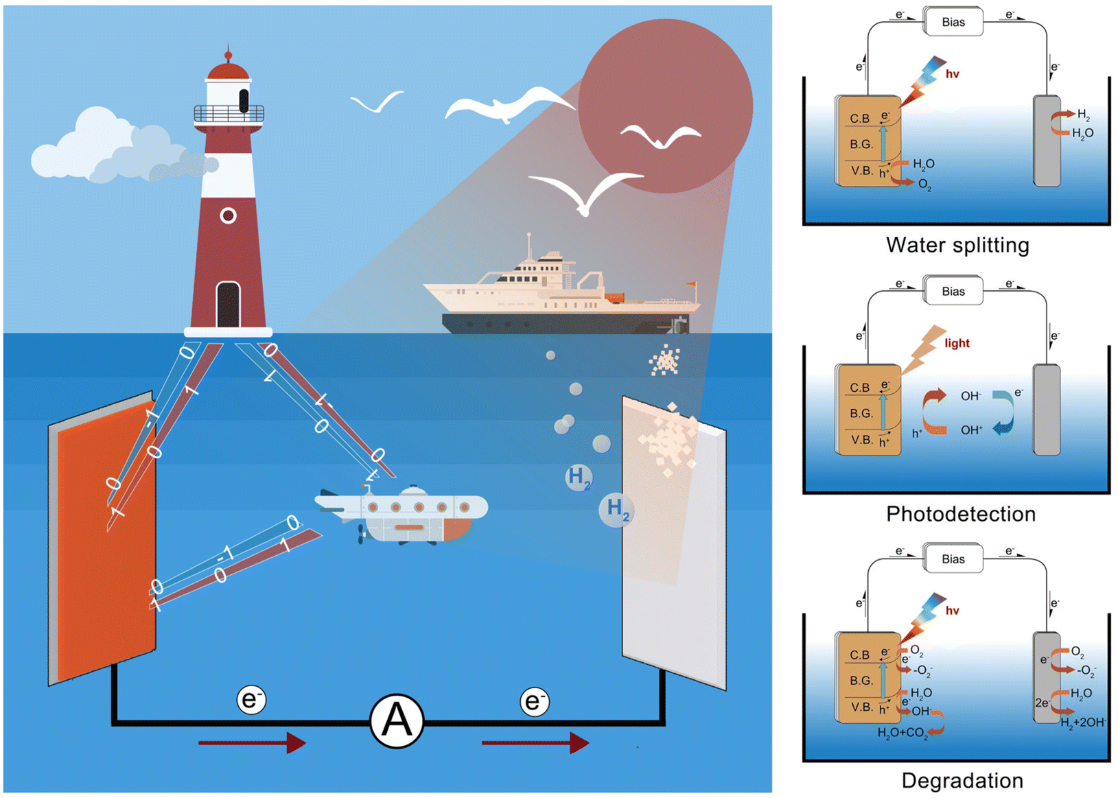 | ||
| Fig. 1 Schematical mechanism for PEC activity. | ||
Since TiO2 electrodes have been used for photoelectrochemical degradation and hydrogen production under ultraviolet light, the PEC-type technique has become a hot research area in academia and industry and attracted widespread attention.9 However, due to its wide bandgap, TiO2 can only utilize the ultraviolet portion of sunlight, resulting in a low energy conversion efficiency.1–3,10–12 Finding suitable visible light-driven semiconductors has been regarded as one of the main research themes in PEC-type applications. Recently, bismuth-based semiconductors have received widespread attention due to their promising optical and electrical properties.13–17 Bismuth (Bi) is a rare heavy metal element in nature with low toxicity and radioactivity, and can be called a “green element”.18 Owing to the existence of 6s2 lone pair electrons, bismuth ions tend to form asymmetrical coordinations with anisotropic crystal structures.19 Hence, Bi-based ionic crystals can be used as multiferroics, superconductors, high ionic conductors, photocatalysts, and photovoltaics.16,17,20–23
Bismuth-based semiconductors are a class of materials with special electronic and optical structures.13–15,20,24 Due to the positive valence band position and strong oxidation ability of most bismuth-based semiconductors, they are ideal catalysts for water splitting and photocatalytic degradation of pollutants.25,26 The optical and electrical properties, like bandgap and carrier mobility, of bismuth-based compounds can be tuned by controlling the anion composition.25,26 Based on these characteristics, the bandgap of bismuth-based compounds can be tuned between 0.1 eV and around 6.0 eV, suitable for broadband photoenergy conversion and detection.25,26 Some bismuth-based compounds possessed very high carrier mobility; for example, the carrier mobility of Bi2O2Se reached up to 450 cm2 V−1 s−1 at room temperature, which was even higher than that of the well-investigated 2D material.27 In addition, bismuth-based semiconductor materials have excellent chemical stability so that BiOI is stable in the laboratory environment for at least 197 days.28 Also, very recently, the 2D in nature bismuth-based semiconductors, like BiOI and Bi2O2Se, have been determined as a kind of novel room-temperature ferroelectric material,29,30 which would be fruitful for PEC-type and electrical applications.
According to the elemental composition, bismuth-based compounds can be mainly divided into binary compounds and ternary compounds. The binary compounds mainly include bismuth oxide, bismuth sulfide, bismuth selenide, bismuth telluride, etc.,26,31–34 while the ternary compounds include bismuth vanadate, bismuth oxyhalides and bismuth oxychalogenides,25,26etc. Until now, there have been over 20![[thin space (1/6-em)]](https://www.rsc.org/images/entities/char_2009.gif) 000 articles containing the keywords Bismuth-based compounds and PEC. Among the investigated bismuth-based semiconductors is bismuth vanadate (BiVO4): BiVO4 is a well-studied bismuth-based oxide that has shown promising performance as a photoanode for PEC water splitting.35–37 BiVO4 has a suitable bandgap for visible light absorption, good charge separation properties, and relatively high catalytic activity. Until now, there are a large number of review articles on BiVO4.38,39 Thus, we just summarized the progress of bismuth binary and mixed-anion compounds in this manuscript. This article mainly discussed bismuth oxide, bismuth sulfide, bismuth oxyhalides, and bismuth oxychalogenides (Fig. 2). This review first introduced the crystal structures and intrinsic properties of these compounds. Then, this article summarized the reported synthesis techniques and challenges that are faced, especially for thin films, although there are few reviews focusing on the film deposition. Lately, the recent PEC-type photodetection and water splitting was introduced and the main issue of PEC stability was analyzed. Finally, this perspective provides an outlook on the application prospects of bismuth-based semiconductors in the field of marine engineering.
000 articles containing the keywords Bismuth-based compounds and PEC. Among the investigated bismuth-based semiconductors is bismuth vanadate (BiVO4): BiVO4 is a well-studied bismuth-based oxide that has shown promising performance as a photoanode for PEC water splitting.35–37 BiVO4 has a suitable bandgap for visible light absorption, good charge separation properties, and relatively high catalytic activity. Until now, there are a large number of review articles on BiVO4.38,39 Thus, we just summarized the progress of bismuth binary and mixed-anion compounds in this manuscript. This article mainly discussed bismuth oxide, bismuth sulfide, bismuth oxyhalides, and bismuth oxychalogenides (Fig. 2). This review first introduced the crystal structures and intrinsic properties of these compounds. Then, this article summarized the reported synthesis techniques and challenges that are faced, especially for thin films, although there are few reviews focusing on the film deposition. Lately, the recent PEC-type photodetection and water splitting was introduced and the main issue of PEC stability was analyzed. Finally, this perspective provides an outlook on the application prospects of bismuth-based semiconductors in the field of marine engineering.
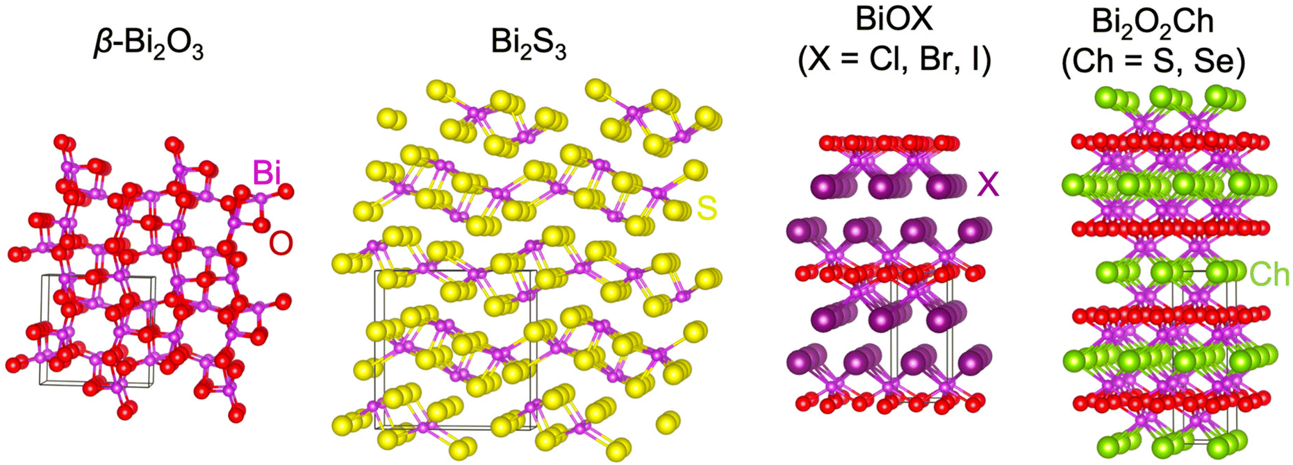 | ||
| Fig. 2 Crystal structure of β-Bi2O3, Bi2S3, BiOX, and Bi2O2Ch. | ||
2. Introduction of bismuth binary and mixed-anion compounds
2.1 Bismuth binary compounds
Bismuth-based binary compounds mainly include Bi2O3, Bi2S3, Bi2Se3, and Bi2Te3etc.26,31–34 Among them, Bi2O3 and Bi2S3 possessed promising photoelectric and photocatalytic properties, which were widely used in photovoltaic devices, optoelectronic devices, and photocatalytic applications.33,34,40 Bi2Se3 is a kind of topological insulator with non-trivial surface states and electronic structures, demonstrating research significance in the fields of topological insulators and quantum bits.31,41 Bi2Te3 is a kind of excellent thermoelectric material, which can be used as thermoelectric modules, converting waste heat into electrical energy, and demonstrates potential applications in energy utilization and energy conservation.42,43 These bismuth binary compounds not only possess rich physical and chemical properties, but also exhibit diverse application prospects, which have important research and application significance. Due to the limitations of the topic selection, this article focused on introducing Bi2O3 and Bi2S3 for PEC-type applications.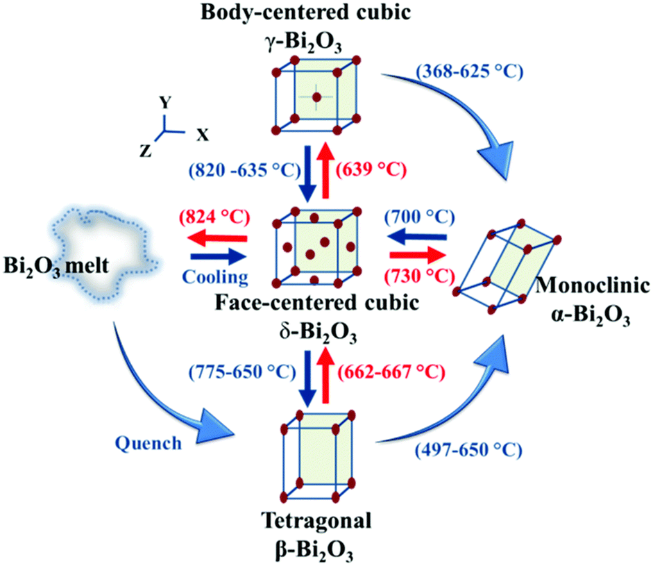 | ||
| Fig. 3 Phase transformation among α-, β-, γ-, and δ-Bi2O3. This figure has been reproduced from ref. 40 with permission from the Royal Society of Chemistry, copyright 2021. | ||
Generally, all the Bi2O3 are direct bandgap semiconductors, with a bandgap between 2–3.96 eV, depending on the crystal structure.40 At the same time, Bi2O3 has a high refractive index, high dielectric constant, excellent photoconductivity, and photoluminescence properties. Among the Bi2O3, δ-Bi2O3 has a complex disordered distribution of oxygen vacancies within the fluorite-like structure, beneficial for ionic conductivity.44 Thus, δ-Bi2O3 has the highest oxygen ion conductivity and can be used as electrolyte materials for solid-state oxide fuel cells and oxygen sensors.45
Metastable β-Bi2O3 is the most attractive for photocatalysis among the Bi2O3, with a minimum bandgap width of 2.1–2.4 eV.40 The narrow bandgap might be raised from the shallow valence band maximum hybridized by the Bi 6s and O 2p orbital.46 The narrow bandgap and suitable conduction and valence band positions of β-Bi2O3 make it a promising photocatalyst for water splitting and other oxidation–reduction reactions.40 In addition, β-Bi2O3 possessed a tunnel-like structure, where the anisotropic structure can efficiently promote the transfer of photogenerated carriers.47 For instance, M. Kim proved the preparation of textured β-Bi2O3 exhibited high stability and photocurrent density owing to the short charge transfer pathway.47,48 Sometimes, α-Bi2O3 was used for photocatalysis, but the performance was not good owing to the large bandgap.40 Based on these characteristics, this review mainly focuses on the β-Bi2O3.
Bi2S3 belongs to n-type semiconductor materials, and its conduction band is formed by hybridization of the 6p level of Bi with the 3p level of S, while the valence band is composed of the 3p level of S, and the contribution of the 6p level of Bi is the smallest.50 The direct bandgap of bismuth sulfide is about 1.3 eV and the absorption coefficient reached about 104–105 cm−1, suitable for harvesting visible light for PEC activity.50,51 Its bandgap energy can be tuned by controlling the size, shape, and composition of the nanoparticles or thin films.50–52 Meanwhile, Bi2S3 has a good electrical property. The resistivity (ρ) of Bi2S3 is measured at 105 Ω cm and the conductivity ranges from 10−6 to 10−7 Ω−1 cm−1 at 300 K.53 The abovementioned advantages made Bi2S3 suitable for photocatalysts,54,55 PEC,56–58 photovoltaics,59–61 energy storage,62,63 and photothermal applications.64
In addition, Bi2S3 has attracted attention for its thermoelectric properties, which make it suitable for thermoelectric applications.52,65,66 Thermoelectric materials can convert waste heat into usable electrical energy or provide efficient cooling by utilizing the Seebeck effect.64,65 In this review, we just focused on the PEC-type applications and the potential applications in marine engineering.
2.2 Bismuth oxyhalide BiOX (X = Cl, Br, I)
Bismuth oxyhalide, BiOX (X = Cl, Br, I), is a class of V–VI–VII mixed-anion semiconductor materials. BiOX is a tetragonal matlockite-type layered material with the asymmetry of P4/nmm, stacking by [X–Bi–O–Bi–X] layers through van der Waals (vdW) interactions (Fig. 2). Each bismuth atom is surrounded by four oxygen and four halogen atoms in the [X–Bi–O–Bi–X] motif, producing an asymmetric decahedral symmetry. The strong intralayer covalent bonds and interlayer van der Waals attraction give BiOX anisotropic structures and properties. Due to induced polarization, this layered structure promotes the formation of an internal electrostatic field perpendicular to the layer.67–69 The built-in electric field is considered to be beneficial for the separation of photogenerated charge carriers and enhancement of the photoelectric chemical conversion efficiency.67–69For all the BiOX, the conduction band minimum is occupied by the Bi 6p orbital. The top of the valence band is dominated by the 2p orbital of the oxygen and the np orbital of the halogen.70,71 However, the contribution of the halogen np state increases with the increase of the atomic number, resulting in a narrower band gap. Generally speaking, the band gap is BiOCl > BiOBr > BiOI in order from largest to smallest.72 BiOI (Eg = 1.8 eV) with a smaller bandgap has better absorption performance in the visible region, while BiOCl with a larger bandgap (Eg > 3.2 eV) is better at absorbing ultraviolet light and can hardly absorb visible light.28,72 Due to the different optical properties, these three compounds behaved differently in PEC reactions.
Carrier mobility also relied on halogen composition and crystallization orientation. Regarding the hole effective mass, BiOCl and BiOBr have a smaller mass along the [010] directions compared with BiOI.70,73,74 Overall, BiOBr generally performs well in terms of electron mobility, followed by BiOCl and BiOI. BiOI shows a heavier electron and hole effective mass in either direction, which may be affected by its small bandgap and larger atom weight. The relatively low electron mobility of BiOCl may be limited by a large bandgap. The worse carrier mobility would lead to an increase in the recombination of the photogenerated carriers. In addition, the crystal orientation and defects may affect the electron transport performance of BiOX.75–78 The electron effective mass of BiOX along the out-of-plane [001] direction is much smaller than the in-plane [010] direction.70,73 Besides, several reports have indicated that the (102) preferred growth of BiOX exhibited a much superior PEC performance to that of (001) orientated BiOX, which might be attributed to the significant band bending, large carrier density, and narrower bandgap.75,76,79 Now, the crystallographic orientation of BiOX has not been carefully controlled via suitable deposition techniques. In addition, there are other phases for the bismuth oxyhalides, like Bi4O5X2, Bi5O7X, etc., which are easily formed during the synthesis process of BiOX.13,25,26,76 The deficiency of halogens also affected the optical and electronic structures of bismuth oxyhalides, like broadening the bandgap. Hence, further research from the point of view of experiment and theory is highly necessary. An in-depth understanding of the bandgap structure and intrinsic properties of these compounds can help guide relevant application research and materials design.
BiOX was widely investigated as the photocatalyst for pollutant degradation and water splitting for dozens of years. Recently, BiOX has been gradually used in photovoltaics like solar cells80,81 and photodetectors,82,83 sensors,8,58 and piezoelectrical devices,84,85 stimulated by their interesting physical properties. Among the BiOX, BiOBr with a moderate bandgap and carrier mobility exhibited better performance in visible light PEC reactions,76 and BiOI showed promising performance in the construction of solar cells80,81 and photodetection.80,82 In summary, the selection of the appropriate material depends on the specific application requirements, which should take into account factors such as bandgap, optical properties, and electronic structure.
2.3 Bismuth oxychalogenides Bi2O2Ch (Ch = S, Se, Te)
Bismuth oxychalogenides, Bi2O2Ch, mainly include Bi2O2S, Bi2O2Se and Bi2O2Te.86–88 Bi2O2S crystallized into orthogonal structures (Table 1 and Fig. 2), and there is a slight distortion between the adjacent [Bi2O2]2+ layers.89 The structure of Bi2O2Se and Bi2O2Te is highly symmetrical, with a tetragonal lattice (I4/mmm), where each Se2− and Te2− is located precisely in the center of a cube composed of 8 Bi atoms, and the [Bi2O2]2+ layers are uniformly arranged along the c-axis. Different from the famous 2D vdWs layered materials like MoS2, Bi2O2Ch is an ionic layered material in which the [Bi2O2]2+ cationic layer and the [Ch]2− anionic layer are alternately stacked along the c-axis through weak electrostatic interactions. The layers are formed by strong covalent or ionic bonds within the layers, while the layers are stacked together by relatively weak electrostatic forces.86,90 Its atomically thin layered structure allows for better electrostatic control and mechanical flexibility. Bi2O2X has the following advantages: (1) high carrier mobility. For example, the carrier mobility of Bi2O2Se reaches 450 and 40000 cm2 V−1 s−1 at 300 and 2 K, respectively, due to their small carrier effective mass.91,92 The carrier mobility is much higher than the famous investigated 2D materials like MoS2.93 (2) Moderate and tunable bandgap.86,90,94 The bandgap of Bi2O2Ch is highly determined by anionic elements, morphology, and thickness. The bandgap of Bi2O2S, Bi2O2Se, and Bi2O2Te was around 1.3, 0.8, and 0.1 eV, covering the ultraviolet to infrared band.87,95–98 (3) Good stability at room temperature, and the bismuth element is less toxic and is abundant.86,91,92
| Material | Crystal system | Space group | Lattice parameters (Å) | Bandgap (eV) | Effective mass (m0) |
|---|---|---|---|---|---|
| Bi2O2S | Orthorhombic | Pnnm | a = 3.874 | 1.3 indirect |
|
| b = 3.84 |
|
||||
| c = 11.92 | |||||
| Bi2O2Se | Tetragonal | I4/mmm | a = 3.88 | 0.8 indirect |

|
| b = 3.88 |
|
||||
| c = 12.16 | |||||
| Bi2O2Te | Tetragonal | I4/mmm | a = 3.98 | 0.1 indirect |
|
| b = 3.98 |
|
||||
| c = 12.70 |
The band structure characteristics of the Bi2O2Ch system are calculated and analyzed using first principles. The conduction band minimum of Bi2O2Ch is mainly composed of both the 2p orbital of the O atom and the 6p orbital of the Bi atom.96,97 At the same time, the valence band maximum consists of the oxygen 2p orbital and the chalcogenide np orbital. As the atomic mass of the chalcogenide increases, the contribution of the oxygen 2p orbital to the electronic state decreased.96,97 Therefore, from Bi2O2S to Bi2O2Se to Bi2O2Te, the bandgap decreased. The optical properties of Bi2O2Ch are anisotropic, as evidenced by the significant disparity in absorption intensity between the in-plane (x/y) and out-of-plane (z) directions, particularly within an energy range of approximately 2 eV above the absorption edge. This anisotropy aligns with the structural anisotropy of the material, where in-plane bonds exhibit strength while out-of-plane bonds are relatively weak.99,100 The observed anisotropy and heightened absorption intensity suggest potential applications for Bi2O2Ch in optoelectronic devices.
Compared with bulk materials like silicon, the Bi2O2Ch have the advantage of flexibility, which makes them capable of overcoming short-channel effects and following Moore's law in terms of scalability.92,101 The unique surface structure and 2D crystal structure of Bi2O2Se make it widely applicative in sensors, memristors and nanogenerators. Various research groups have already demonstrated the potential of Bi2O2Ch-based electronic devices, with Bi2O2Ch FETs exhibiting high carrier mobility and a large driving current.86,94,102–104 Simple logic gates have been made from Bi2O2Ch. Besides, Bi2O2Ch is also an exceptional choice for infrared photodetectors due to its narrow bandgap and high mobility,105–109 and its strong spin–orbit coupling effect and ferroelectricity contributing to a large thermoelectric ZT value.110 Among the Bi2O2Ch, Bi2O2Se is intensively investigated followed by Bi2O2S. Compared with Bi2O2S and Bi2O2Se, the bandgap of Bi2O2Te is only about 0.1 eV, which is not suitable for application in photocatalytic hydrogen production and pollutant degradation alone.111 Perhaps it can play a certain role as an electron transport layer and broaden the light absorption range. Given this, this review article does not discuss Bi2O2Te.
3. Fabrication techniques of bismuth binary and mixed-anion compounds
Generally, bismuth binary and mixed-anion compound nanoparticles have been widely synthesized through various simple techniques such as chemical precipitation, sol–gel methods, hydrothermal methods, solid phase reactions etc.14,33,40 The high surface-to-volume ratio and controllable surface morphology of 3D state nanostructures have endowed various potential applications including catalysis, drug delivery, and sensors. To achieve the PEC reaction, spin-coating or drop-casting the as-synthesized nanoparticles on the conducting substrate is necessary for the photoelectrodes’ construction (Fig. 4). While these methods are very simple, it is challenging to fully cover the substrate with nanostructures. In addition, coated nanostructures were easily peeled off from the substrates once immersed in an electrolyte owing to the poor attachment.14,112 Compared with the micron or nanoscale structures, continuous thin films deposited via advanced techniques are more suitable for the construction of large-area PEC-type devices. Besides, thin films are beneficial for the investigation of intrinsic properties such as electrical conductivity and optical coefficient. However, the deposition techniques for the thin films are usually complicated and expensive. Thus, in this part, we reviewed the fabrication techniques of bismuth binary and mixed-anion compounds from the perspective of nanoparticle synthesis and thin film deposition.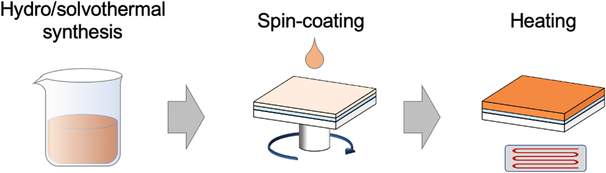 | ||
| Fig. 4 Typical schematical image for the preparation of photoelectrodes from nanoparticles. | ||
3.1 Nanoparticle synthesis
There are a large number of reports and reviews on the nanoparticle synthesis of bismuth binary and mixed-anion compounds.14,33,40 Thus, in this part, the authors did not introduce it in detail but just point out the facing challenges and recent report.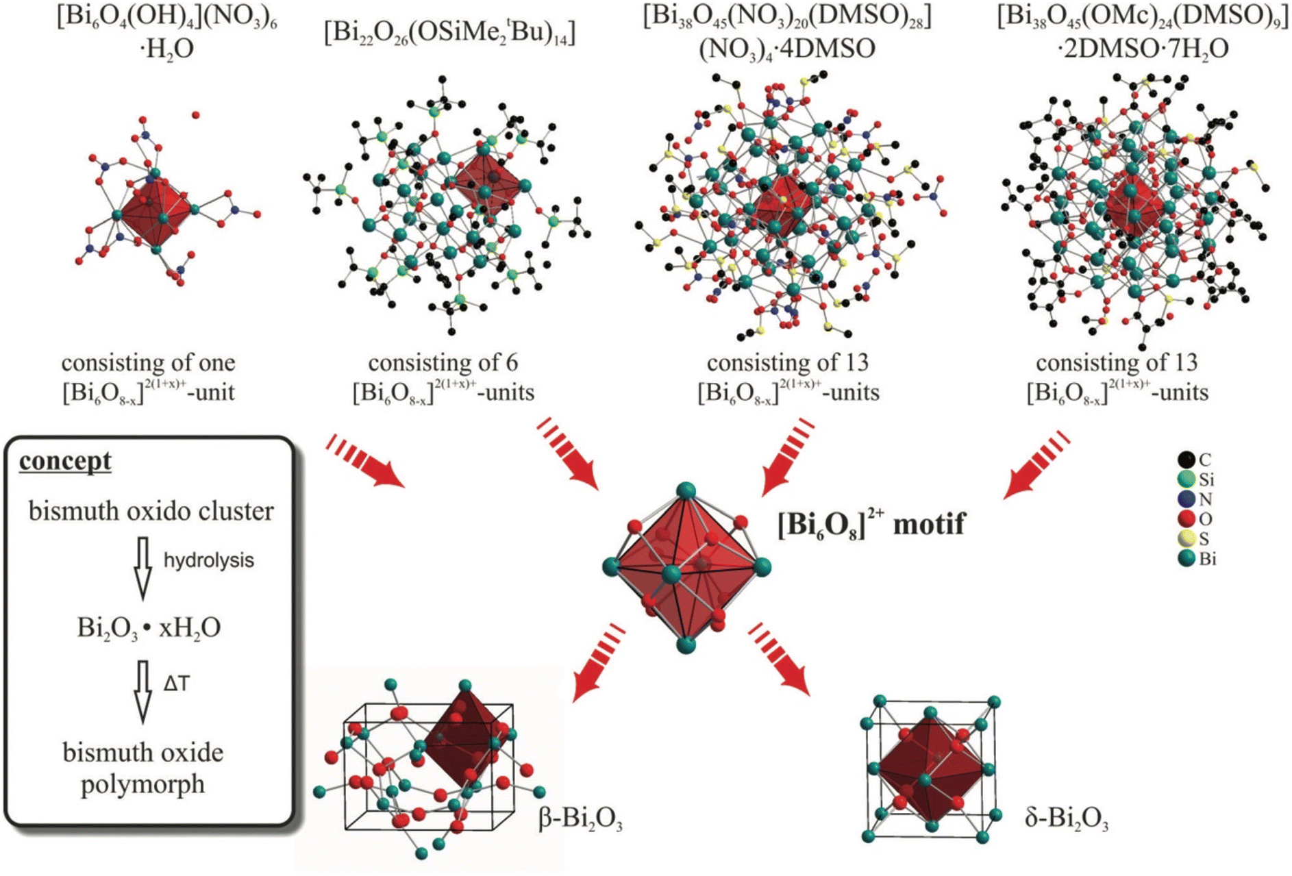 | ||
| Fig. 5 Hydrolysis synthesis of β- and δ-Bi2O3 starting from various bismuth oxide clusters with a similar structure to Bi2O3.120 This figure has been adapted/reproduced from ref. 120 with permission from the Royal Society of Chemistry, copyright 2013. | ||
β-Bi2O3 nanowires were synthesized by metal oxide vapor transport deposition and metal–organic chemical vapor deposition (CVD).121,122 In the former method, nanoscale bismuth droplets are oxidized by O2 at a moderate temperature of 250–350 °C, resulting in ultrathin β-Bi2O3 nanowires with a diameter of 7 nm and a length of several micrometers, which can be controlled by the collection zone temperature of the CVD furnace.121,122 For metal–organic CVD, O2 and trimethyl bismuth are used as precursors of oxygen and bismuth, respectively.122 At 400 °C, β-Bi2O3 wire with a diameter between 30–90 nm is obtained, while a cluster or membrane structure is obtained between 450 °C and 500 °C. To further increase the reaction surface area, hollow microsphere-like β-Bi2O3 was successfully prepared by using the carbon nanospheres as sacrifice templates.123
In summary, choosing a suitable precursor is the prerequisite for the controllable synthesis of β-Bi2O3. Besides, the formation of the beta-phase is kinetically controlled. Achieving high phase purity and avoiding the conversion to the α phase often requires the precise control of reaction parameters such as temperature, reaction time, and heating/cooling rates. In addition, controlling the particle size, shape, and morphology of β-Bi2O3 during synthesis is still challenging. Overcoming these difficulties often requires a combination of careful experimental design, optimization of synthesis parameters, and the use of appropriate additives, precursors, or reaction conditions.
In the case of Bi2S3 synthesis, the hydrothermal approach is typically conducted at temperatures below 200 °C.52,125,126 In some cases, continuous stirring is employed alongside the hydrothermal method. By utilizing this method, one-dimensional structures of Bi2S3 including nanotubes, nanowires, and nanorods have been successfully synthesized. A unique approach involves the synthesis of hedgehog-like Bi2S3 micro/nanostructures using a soft-template composed of trimetallic acid and cetyltrimethylammonium bromide, which acts as a cationic surfactant.127 Another variation of the hydrothermal method utilizes thiourea as a sulfur source, resulting in diverse Bi2S3 morphologies such as nanorods and nanoflowers. The reaction carried out at 180 °C involves a 2:3 ratio of hydrated bismuth and thiourea with the addition of nitric acid under continuous stirring.128 Benefiting from the merits of solution-based methods, it is easy to modulate the morphology of nanoparticles by changing the solvent. To enhance the efficiency of the hydrothermal synthesis of Bi2S3, certain chemicals should be added, which promote the crystallization of Bi2S3.
Compared with hydrothermal methods, the solvothermal process requires the organic solvent as the medium for the preparation of Bi2S3, while the organic solvent may contain toxins and is more expensive than water. Both methods are low-cost in setup and energy. In addition, the sol–gel method,129 mechanical milling,130,131 microwave-assisted methods,132 and solid phase reaction133 were used for the synthesis of Bi2S3. Although these methods exhibited special merits in the synthesis of Bi2S3, the purity of the synthesized Bi2S3 is not very high owing to the difficulties in controlling the reaction process precisely. Currently, achieving the fast and green synthesis of Bi2S3 is highly necessary. Bismuth and sulfur precursors used in the synthesis of Bi2S3 can be difficult to handle due to their reactivity and sensitivity to air and moisture. Special precautions need to prevent oxidation or undesirable reactions during precursor handling and synthesis. Meanwhile, the synthesis of Bi2S3 involved slow reaction kinetics and required long reaction times or elevated temperatures. Optimizing the reaction conditions, such as temperature, reactant concentrations, and reaction time, is necessary to promote a complete reaction and obtain high-quality Bi2S3 crystals. In addition, achieving the desired stoichiometry of Bi2S3 can be challenging. The reaction conditions and ratios of bismuth and sulfur sources need to be carefully controlled to obtain the desired composition and avoid the formation of undesired phases or impurities.
1D nanostructures like wires and fibers, owing to the large surface area–volume ratio, are suitable for photocatalytic and PEC applications. Recently, the templated method was used for the deposition of nanowires/fibers in which nano-porous anodized alumina and activated carbon fiber can be used as templates. BiOCl nanofibers were synthesized by adding polyacrylonitrile to viscous N,N-dimethylformamide solution.139
As for 2D sheets like BiOX, these are generally synthesized with CVD on very flat substrates, like mica and oxide single crystals.140,141 The crystals of BiOX generally exhibit a sheet-like morphology, which is characteristic of their layered crystal structure. To synthesize these crystals, precursors such as powder BiOX and BiX3 are placed in a reactor tube and thermally vaporized.80,83,141 The resulting vapors are transferred onto a substrate surface positioned at a lower temperature region. By adjusting the experimental conditions and deposition time, the size of the crystals can be controlled, typically ranging from micro- to nano-scale in the lateral direction and the vertical direction, respectively.77 These crystals often possess a flat surface, making them suitable for constructing multilayer devices and facilitating the measurement of physical properties such as conductivity.
Compared with 1D and 2D BiOX, 3D BiOX, like nanoflowers, was easily formed during the synthesis process. These 3D nanostructures are typically composed of aggregated 2D sheets, reflecting the layered crystal structure and its anisotropic nature.142–144 The morphology of these microcrystals is heavily influenced by experimental conditions, including the pH and reaction temperature. For instance, a solution containing Bi(NO3)3 dissolved in nitric acid can be subjected to heat treatment with the addition of sodium halide, polyvinylpyrrolidone, and citric acid to produce spherical microstructures of BiOX.145,146 The halogen composition can be precisely controlled by adjusting the concentration of sodium halide, which is a significant advantage of the solution-based process. The concentration of additives, such as polyvinylpyrrolidone and citric acid, plays a crucial role in determining the morphology of the resulting microstructures.145,146 In the solvothermal reaction, where BiCl3 is dissolved in a mixture of ethanol and water, the morphology of BiOCl can be altered by varying the concentration of citric acid.145 Nanosheets can transform into nanoplates, and nested structures can form hollow spheres as the concentration of citric acid is increased. This result demonstrates that citric acid not only serves as a crystal growth inducer but also acts as a structural guide agent, influencing the morphology of BiOCl.
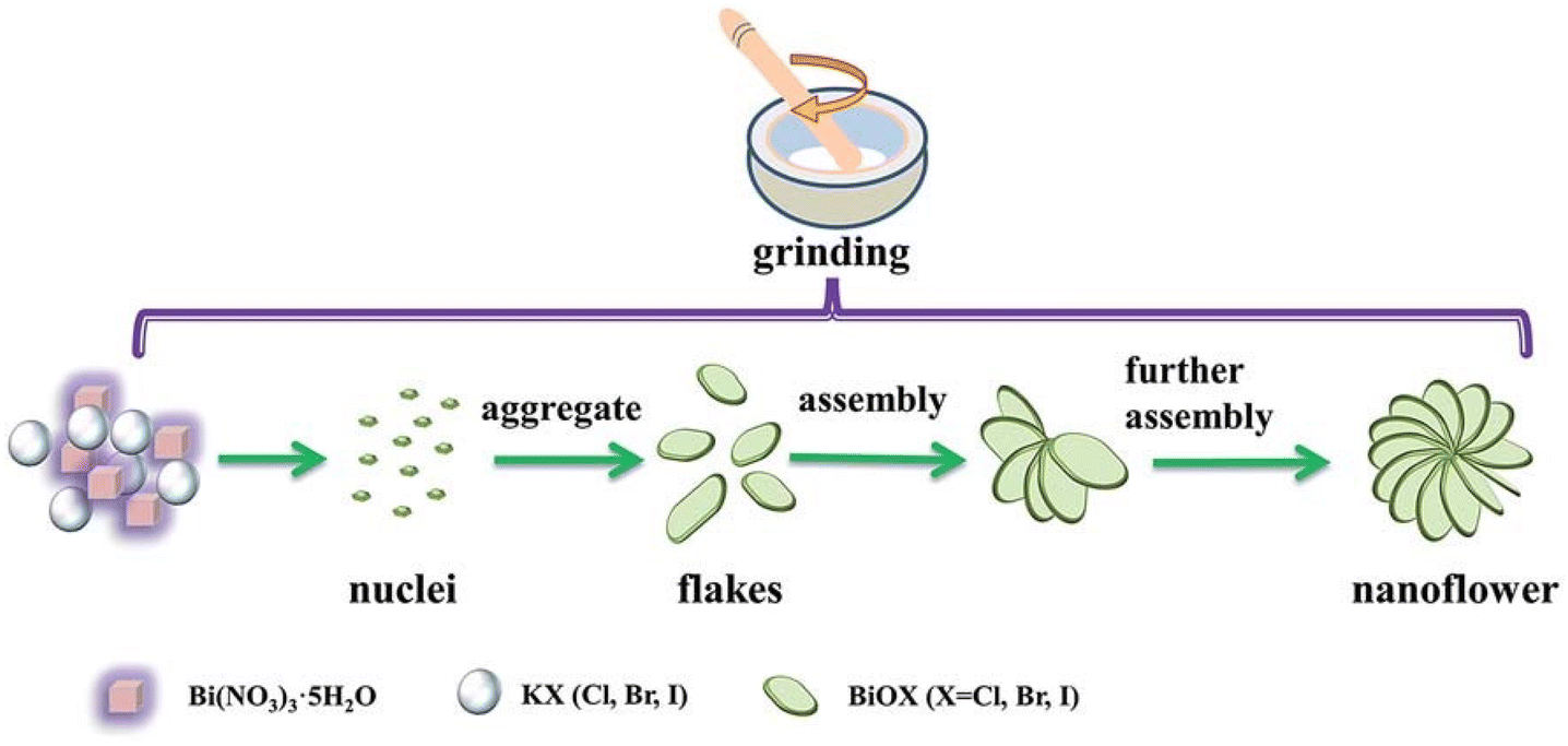
Recently, solvent-free mechanical grinding methods have also been used for the preparation of BiOX (Fig. 6).135 BiOX fractional flower-like nanostructures were synthesized by mixing and grinding Bi(NO3)3 with KX. During the grinding, the HNO3 acid formed in the product promotes the further reaction of Bi(NO3)3 and the nucleation of BiOX. With the increase in grinding time, the single-layer laminate was assembled into a flower-like nanostructure. This method is much simpler and greener than the conventional solvent-based synthesis techniques, which are suitable for industrial application. However, further optimization of the synthesis condition is necessary to enhance the purity and control the surface morphology of BiOX. Besides, achieving and maintaining the desired stoichiometry of bismuth oxyhalide nanoparticles is challenging. Variations in the reaction parameters, such as temperature, time, precursor concentration, and other reaction conditions, can impact the stoichiometry and composition of the synthesized nanoparticles. In addition, BiOX nanoparticles are prone to aggregation or stability issues, leading to unwanted particle growth or changes in properties. Incorporating appropriate stabilizing agents or surface modifications, such as surfactants or ligands, can enhance the stability and prevent the aggregation of the nanoparticles.
3.2 Thin film deposition
Although thin film is much more suitable for the PEC-type applications, the number of reports on the thin film deposition of bismuth binary and mixed-anion compounds is much less than that on the format of nanopowders. Also, compared with well-investigated oxide and 2D materials, the deposition techniques of bismuth binary and mixed-anion compounds still need further investigation. This part mainly discussed the previously reported film deposition techniques for the bismuth binary and mixed-anion compounds and pointed out the challenges.| Method | Temperature | Precursor | Ref. | |
|---|---|---|---|---|
| PVD | Thermal evaporation and post annealing | Annealing at 300 °C | Bi (001) film, BiOx amorphous film | 156 |
| Sputtering and post annealing | 200–600 °C | Bismuth metal, Bi2O3 | 157–159 | |
| CVD | Aerosol-assisted CVD | 300–450 °C | Bismuth carbamate | 161 |
| MOCVD | 450 °C | Bi(OtBu)3 | 162 | |
| Mist CVD | 350–600 °C | Bismuth(III) 2-ethylhexanoate | 163 | |
| Solution-based techniques | Photochemical synthesis | 250 °C | Bismuth(III)-N-methyldiethanolamine complex | 45 |
| Spray pyrolysis | 450 °C | Bismuth(III) acetate | 164 | |
| Spin-coating and post annealing | 370 °C | Bi38O45(OMc)24(DMSO)9·2DMSO·7H2O | 165 | |
| 300–450 °C | Bi(NO3)3·5H2O | 166 | ||
| Electrodeposition and post annealing | RT and annealing at 200–600 °C | Bi(NO3)3·5H2O, acid/NaOH | 167 and 168 | |
| Microwave-assisted chemical synthesis and post annealing | 300 °C | Bi(NO3)3·5H2O | 169 | |
CVD involves transferring gaseous precursors onto a heated substrate surface, where they undergo a chemical reaction to form a thin film.162 The quality of the film largely depends on the specific precursor used. In previous studies on the chemical vapor deposition of β-Bi2O3, bismuth(III) tert-butanol was used as a precursor, resulting in microcrystals with diameters ranging from 0.4 to 2 μm.162 By controlling the flow rate of bismuth precursors, homogeneous β-Bi2O3 films were successfully obtained on Si (100) and Al2O3 substrates.170
In comparison with traditional physical and chemical vapor deposition methods, the solution deposition method is commonly employed for the thin film growth of β-Bi2O3.45,164–169,171 This approach offers several advantages, such as the wide choice of precursors and a simple experimental setup that can be adjusted based on the chemical properties of the reactants and products. Atmospheric pressure is favorable for preventing bismuth evaporation, while low temperatures are conducive to obtaining metastable β-Bi2O3. Various solution-based methods for β-Bi2O3 deposition have been reported. For example, one approach involves the ultrasonic spraying of a tetrahydrofuran solution containing [Bi38O45(O2CC3H5)24 (DMSO)9]·2DMSO·7H2O, which is then hydrolyzed and annealed to obtain a thin film with an α- or β-Bi2O3 bulk structure at 550 and 370 °C, respectively.165
In another report, a solution of bismuth(III) N-methyldiethanolamine was spun onto a glass or polyimide substrate to form an amorphous film that crystallized to β-Bi2O3 under ultraviolet irradiation in O2 at 250 °C (Fig. 7a).45 Deposition from bismuth metal electrodes at room temperature by electrochemical methods has been reported (Fig. 7b).167,168,171 β-Bi2O3 films are formed on platinum or graphite rods by the anodic oxidation of citric acid or NaOH aqueous solutions, and subsequent annealing improves the crystallinity of the films. To achieve the electrochemical deposition, the substrate is limited to conducting materials. Very recently, (201) β-Bi2O3 epitaxial thin films on α-Al2O3 (0001) single crystal substrates were deposited through mist CVD via choosing bismuth(III) 2-ethylhexanoate as the precursor (Fig. 7c). The morphology and crystallinity of β-Bi2O3 were highly dependent on the deposition temperature: a high temperature led to the aggregation of thin films and a low temperature resulted in formation of the amorphous film. Short-time high-temperature (600 °C) post-annealing was beneficial for the enhancement of the crystallinity and surface flatness, while slightly long-time annealing will cause the degradation of thin film quality (surface roughness and crystallinity).163 As far as we know, this is the first report on the epitaxial growth of β-Bi2O3; however, owing to the complicated deposition process, this method is not suitable for industrial application.
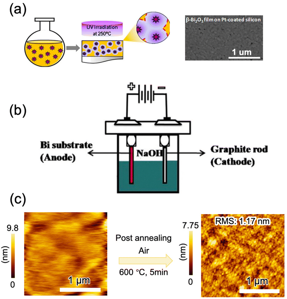 | ||
| Fig. 7 β-Bi2O3 thin film deposited by (a) a photochemical solution method,45 adapted from ref. 45 with permission from Springer Nature, copyright 2016; (b) electrochemical deposition,172 adapted from ref. 172 with permission from Elsevier, copyright 2016; and (c) solid-phase epitaxy via mist CVD,163 adapted from ref. 163 with permission from the American Chemical Society, copyright, copyright 2019. | ||
Similar to nanoparticles, special synthesis techniques, optimization of deposition conditions, and the inclusion of additives may be necessary to stabilize the β phase and prevent phase transformation. Normally, post annealing to improve the crystallinity of β-Bi2O3 is necessary for most film deposition methods, which posed challenges in controlling phase purity and energy saving. In addition, annealing at higher temperatures than 200 °C would cause the decomposition of β-Bi2O3. In that sense, annealing at high temperatures to stabilize β-Bi2O3 is not a good method. Meanwhile, organic compounds are usually used as precursors for the deposition of β-Bi2O3, where the issue of carbon residues needs to be considered. To some extent, carbon residues will degrade the photoresponse performance. Thus, overcoming these challenges is necessary for the broad practical usage of β-Bi2O3.
 | ||
| Fig. 8 Bi2S3 deposited by (a) spin-coating method,176 adapted from ref. 176 with permission from the American Chemical Society, copyright 2018; (b) CVD deposition,178 adapted from ref. 178 with permission from Wiley, copyright 2020; and (c) dual-source mist CVD,181 adapted from ref. 181 with permission from the American Chemical Society, copyright 2022. | ||
| Technique | Precursors | Process | Ref. | |
|---|---|---|---|---|
| Two-step | Electrochemical deposition | CH3CSNH2, C12H10BiK3O14 or Bi(NO3)3·5H2O | (1) Deposition of bismuth film | 182 and 183 |
| (2) Oxidized into Bi2O3 | ||||
| (3) Vulcanized to Bi2S3 | ||||
| Sputtering and solution-assisted method | Bi2O3, CH4N2S | (1) Synthesis of Bi2O3 thin film by radiofrequency sputtering | 179 | |
| (2) Hydrothermal treatment for 3 h | ||||
| Chemical vapor deposition (CVD) | Bi metal, S | (1) Synthesis of Bi2O3 exfoliated from Bi | 178 | |
| (2) Vulcanized to Bi2S3 | ||||
| Spin coating | Bi(NO3)3·5H2O, Na2S·9H2O | (1) Synthesis of Bi2S3 powder | 184 | |
| (2) Film deposition | ||||
| C6H9BiO6, CH4N2S | (1) Deposition of amorphous Bi2S3 film | 176 | ||
| (2) Crystallized under H2S gas | ||||
| Hydrothermal method | Na2S2O3, Bi(NO3)3 | (1) Deposition of intermediates films at 600 °C for 12 h | 185 | |
| (2) Annealed at 150–250 °C | ||||
| Successive ionic layer adsorption and reaction | Bi(NO3)3, Na2S·9H2O | (1) Two-step dipping process | 186 | |
| (2) Post annealing | ||||
| One-step | CVD | Bi2S3 nanopowders | Evaporation of precursor at 600 °C and deposited at 500 °C | 59 |
| Metal–organic CVD | Secondary amine, CS2, Bi2O3 | (1) Synthesis of the metal–organic precursor Bi(S2CNEt2)3 | 180 | |
| (2) Film deposition | ||||
| Mist CVD | BiCl3, thiourea | Dissolved in DMF solvent, atomized into mist, deposited at 450 °C | 181 | |
Very recently, mist CVD, a kind of green and open-air pressure solution-based method, has demonstrated the fast deposition of Bi2S3 thin films via applying the less toxic, cheap, and commercially available BiCl3 and thiourea as the precursors (Fig. 8c).181 To our knowledge, this is the simplest method for the synthesis of high-quality Bi2S3 film, while the surface morphology is rough and discontinuous. Hence, developing facile techniques to prepare uniform and continuous Bi2S3 thin films is still highly necessary. Until now, discontinuous thin films were obtained in which the synthesized Bi2S3 thin films were composed of nanowires and/or nanoplates. Especially, enormous efforts should be devoted to the surface morphology modulation of Bi2S3 thin films.181 Besides, the crystallization temperature is normally higher than 400 °C which is not suitable for some organic-based flexible substrates and energy saving. Besides, there are no epitaxial Bi2S3 thin films, which might be attributed to the anisotropic crystal structure. Thus, finding suitable precursors to decrease the deposition temperature of Bi2S3 may be beneficial for broadening the application of Bi2S3.
3.3 BiOX (X = Cl, Br, I)
CVD is one of the most commonly used techniques for the deposition of BiOX from bismuth halides. Dating back to 1998, BiOxIy thin films were deposited on MgO (100) substrates with CVD from BiI3 and O2.187 In the conditions examined, the growth window of stoichiometric BiOI was very small, and iodine deficiency was observed in the most of checking experimental conditions. In addition, the surface of the substrate was not fully covered by the film. Recently, BiOX in the format of nanoplates with the size of around tens of micrometers was deposited via CVD in which the substrate is not fully covered by the nanoplates (Fig. 9a).80,82,83,141,188–191 Currently, there are nearly no reports of BiOX thin films deposited via the vacuum-based technique, which might be attributed to the difficulty of controlling the chemical composition due to very volatile halides and bismuth. | ||
| Fig. 9 Schematic diagram of preparing BiOX thin films using (c) CVD,83 adapted from ref. 83 with permission from Wiley, copyright 2020; (b) SILAR,193 adapted from ref. 193 with permission from Wiley, Elsevier, copyright 2018; and (c) aerosol-assisted CVD.76 adapted from ref. 76 with permission from the Royal Society of Chemistry, copyright 2016. | ||
Instead, solution-based approaches for depositing continuous BiOX thin films are frequently documented.76,79,192–196 One of the simplest methods is the SILAR method (Fig. 9b).193 Immersing the glass substrate coated with FTO in a solution containing bismuth and halogen precursors resulted in the formation of a BiOX film.193 The film comprises aggregated nanosheets that grow vertically on the substrate. Immersing the substrate in HF, HCl, and KBr solution also facilitates the conversion of Bi2O3 film into BiOX at room temperature.72 However, the conversion is not fully complete for bismuth oxyiodide. As in the case of the SILAR method, the obtained film consists of nanosheets.
Another straightforward solution-based technique is spray pyrolysis.197 In this process, a solution of Bi(NO3)3 and NH4I glycol solutions is sprayed onto a heated substrate, where a film is formed through the evaporation and chemical reaction of the precursor. The deposition temperature played a crucial role in determining the morphology and composition of the films.197 Like the impregnation method, the resulting film is composed of nanosheets. AACVD, combing the merits of vapor and solution deposition techniques, is applied to BiOX films (Fig. 9c).76,194 The bismuth halide N,N-dimethylformamide solution was atomized with a piezoelectric device and transferred to a heated FTO-coated glass substrate. The resulting film consists of nanosheets with improved flatness and density. Very recently, mist CVD, similar to AACVD, was widely used for the deposition of BiOX epitaxial and polycrystalline thin films. By choosing perovskite-type oxides like SrTiO3 as the substrates, the BiOX showed epitaxial growth so that the obtained thin film possessed high crystallinity and an atomic flat surface.198 Also, on the polycrystalline conducting glass substrate, the preferred orientation of BiOX was tuned by controlling the deposition temperatures.79,195,196 Also, the thickness of BiOX thin films was controlled by tuning the precursor concentration and deposition time.189,198 However, it is very hard to obtain very thick BiOX thin films with mist CVD. In addition, BiX3 is very easily hydrolysed into other compounds which is not suitable for the deposition of BiOX. Adding an acid reagent can prevent the hydrolysis of BiX3, which also degrades the obtained BiOX thin films. The epitaxial thin films are suitable for the construction of high-performance PEC-type devices. However, the epitaxial growth is highly dependent on the single crystal substrates. Until now, commercially available conducting single crystal substrates have been very limited. Overall, finding suitable precursors, substrates, and deposition techniques is highly necessary for the deposition of BiOX thin films.
3.4 Bi2O2Ch (X = S, Se)
Attracted by the very high carrier mobility of Bi2O2Ch, film deposition techniques have shown great improvement during recent years. At present, the Bi2O2Ch film deposition techniques mainly include the liquid phase method,101,199 physical/chemical vapor deposition,200 molecular beam epitaxy,201 and other technologies.150,199Table 4 briefly summarized the reported Bi2O2Ch thin film deposition techniques. Bi2O2S films are mainly prepared by chemical bath deposition and spin coating. Bi(NO3)3·5H2O and thiourea or Na2S were used as precursors, and alkaline solutions (KOH, NaOH) were added to accelerate the formation of Bi2O2S. The reaction time of the Bi2O2S prepared by this method is usually long, and the surface of the Bi2O2S prepared is rough and nanoflower-like.147,150,202 The primary method for preparing Bi2O2Se is chemical vapor deposition, which typically uses Bi2O3 or Bi2Se3 as the precursor.91,140,203 By precisely controlling the parameters of the film deposition and selenization or oxidation processes, the deposition of Bi2O2Se films can be successfully achieved (Fig. 10a). Bi2O2Se epitaxial thin films with precise control over thickness down to the monolayer were demonstrated on TiO2-terminated SrTiO3 through MOCVD.204 In addition, high-quality Bi2O2Se epitaxial thin films with high crystallinity and a flat surface have been synthesized by molecular beam epitaxy (MBE, Fig. 10b).201 However, the MBE method is not suitable for industrial-scale production owing to the expensive setup and difficulties in the synthesis of large-size epitaxial thin films.201 | ||
| Fig. 10 Schematic diagram of preparing Bi2O2Se thin films using (a) CVD,206,207 adapted from ref. 206 and 207 with permission from the American Chemical Society, copyright 2017 and 2019; (b) molecular beam epitaxy,201 adapted from ref. 201 with permission from Wiley, copyright 2019 and (c) solution-assisted deposition with spin-coating deposition and annealing,101 adapted from ref. 101 with permission from the American Chemical Society, copyright 2019. | ||
| Method | Bi Source | Ch Source | Condition | Sample form | Ref. | |
|---|---|---|---|---|---|---|
| Bi2O2S | Hydrothermal + spin coating | Bi(NO3)3·5H2O | Thiourea | Alkaline solution, 12 h | Nanosheet ∼ 100 nm | 147 |
| C6H13BiN2O7·H2O | Thiourea | KOH solution | Nanosheet ∼ 2 μm | 150 | ||
| Bi2O3 | Thiourea | 40 h, 180 °C | Nanosheet ∼ 100 nm | 202 | ||
| Chemical bath deposition | Bi(NO3)3·5H2O | Thiourea | 200 °C, 80 min | Nano-flower-like film | 199 | |
| Bi(NO3)3·5H2O | Na2S | 30 °C, 4 h | Continuous film | 205 | ||
| Bi2O2Se | CVD | Bi2O3, Bi2Se3 | 500–700 °C | Nanosheet ∼ 200 μm | 140 | |
| Bi2O3 | Se | 680 °C | Nanosheet ∼ 250 μm | 91 | ||
| Bi2Se3, O2 | Salt assisted, 500 °C | Nanosheet ∼ 500 μm | 203 | |||
| MOCVD | Bi(Ph)3, (CH3)2Se2 | 350 °C | Epitaxial thin films | 204 | ||
| Pulsed laser deposition | Bi2O2Se prepared by Bi2O3, Bi, Se | 375 °C, 0.71Pb(Mg1/3Nb2/3)O3–0.29PbTiO3 | Epitaxial thin films | 200 | ||
| Molecular beam epitaxy | Bi | Se | SrTiO3 | Epitaxial thin films | 201 | |
| Hydrothermal + spin coating | Bi(NH3)2C6H7O7 | Na2SeO3 | Alkaline solution, 12 h | Nanosheet ∼ 2 μm | 150 | |
| Solution-assisted | Bi2O3 film by spin coating | Se | Air annealed, selenized | Continuous film | 101 | |
In recent studies, wafer-scale Bi2O2Se epitaxial thin films have been successfully grown on perovskite-type oxide single crystal substrates such as LaAlO3, SrTiO3, and (La, Sr)(Al, Ta)O3.86,204,206 These perovskite-type oxides possess a similar crystal structure to Bi2O2Se, resulting in a small lattice mismatch between the substrate and the film. By utilizing these perovskite-type oxide single crystals as substrates, high-quality Bi2O2Se thin films with controllable thicknesses and wafer sizes were obtained.206 Except for the small lattice mismatch, the strong interatomic interaction at the interface of the Bi2O2Se and SrTiO3 promoted the epitaxial growth of Bi2O2Se, which initiates at the Bi–O layer at the SrTiO3 interface.204 These findings emphasized the significance of selecting suitable substrates for achieving large-size 2D single crystals and provided insights for the synthesis of large-size Bi2O2S and Bi2O2Se epitaxial thin films.
To achieve the epitaxial growth of Bi2O2Se, it is commonly necessary to utilize oxide single-crystal substrates. However, there are several challenges arising from the limitations associated with these substrates. The size of the oxide single crystal substrate limits the preparation of large-size Bi2O2Se epitaxial thin films.86,206,207 Most of these substrates are insulators, which are not suitable for the construction of PEC-type devices. Achieving the exfoliation of thin film is necessary. However, the Bi2O2Se epitaxial thin films grown on oxide single crystal substrates are limited by the strong binding force between the Bi2O2Se and the substrate, making it difficult to exfoliate the thin film from the substrate.208,209 Additionally, Bi2O2Se grown on a mica substrate is prone to achieving thin film exfoliation and transfer, but mica is hard to remove completetly during the transfer process.208,209 Besides, some perovskite-type oxide single crystal substrates are expensive and not suitable for large-scale applications.
Although the advanced thin film techniques, like CVD and MBE,200,201 exhibited various advantages in high-quality Bi2O2Se thin film deposition; these abovementioned thin film deposition methods have high requirements for atmosphere and temperature, and the deposition equipment is relatively expensive. Compared with these techniques, solution-based techniques probably achieve the facile synthesis of Bi2O2Se thin films.210–212 The solution-assisted method first spin-coated Bi2O3 thin films, which were annealed under Se vapor to generate Bi2O2Se (Fig. 10c).101 The prepared thin film has a large size of 2 cm, a controllable thickness, and a continuous and smooth surface, demonstrating high potential in the large-scale preparation of Bi2O2Se. However, there are few reports on the efficient preparation of Bi2O2Se thin films using solution-based deposition techniques, possibly due to the limitations of traditional liquid-phase methods in precursor selection and film rate control. To achieve the efficient preparation of Bi2O2Se thin films by the liquid-phase method, further optimization is needed in selecting suitable precursors, simplifying the deposition process, improving the quality of thin films, and preparing large-sized thin films.
For the deposition of Bi2O2Se and Bi2O2S, it is very important to ensure the phase purity as Bi2Se3 or Bi2S3 might be formed during the synthesis process.213 Therefore, conditions such as temperature, pressure, and reaction time affected phase purity and crystallinity. In addition, the morphology of the material determined its application in photoelectric chemistry and photocatalysis. It may be necessary to achieve the preparation of Bi2O2Se and Bi2O2S with specific morphologies, like nanoflower or nanowire. As pointed out in the nanoparticle part, understanding the crystal growth mechanism of Bi2O2Se is necessary. By overcoming these challenges, high-quality Bi2O2Se and Bi2O2S thin films can be facilely synthesized, and their application potential in PEC, photocatalysis, photovoltaic, and other fields can be expanded.
4. PEC applications of bismuth binary and mixed-anion compounds
4.1 PEC-type photodetection
PEC-type photodetectors are a class of photodetectors that utilize the photoelectrochemical reaction to convert light into electrical signals. PEC-type photodetectors consist of a photoactive material, electrolyte, and appropriate electrode configurations (Fig. 11).7,214,215 The photoactive material serves as a light absorber and generates electron–hole pairs when exposed to light. These photoexcited charge carriers then migrate to the electrode–electrolyte interface, where they engage in redox reactions with the electrolyte. The resulting photocurrent or photovoltage is measured to detect and quantify the incident light. | ||
| Fig. 11 Setup of a PEC-type photodetector.216 This figure was adapted from ref. 216 with permission from Wiley, copyright 2024. | ||
PEC-type photodetectors offer several advantages, such as high sensitivity, tunable spectral response, and the ability to operate under various lighting conditions.7,214,215 They are highly sensitive to light due to their efficient conversion of absorbed photons into photocurrent or photovoltage. The spectral response of PEC-type photodetectors can be tuned by selecting or engineering the photoactive materials with specific bandgaps. Moreover, PEC-type photodetectors can be designed to be flexible and conformable, enabling integration onto unconventional substrates or curved surfaces. This flexibility opens up opportunities for use in wearable devices, flexible electronics, and integrated systems.
Different types of photoactive material can be utilized in PEC-type photodetectors, including semiconductor materials like metal oxides, organic semiconductors, quantum dots, or hybrid structures. The choice of materials depends on factors such as the desired spectral response, stability, and efficiency. Additionally, PEC-type photodetectors can be combined with other functionalities, such as energy conversion or sensing capabilities, to create multifunctional devices. This integration enables the development of compact and versatile systems for various applications. Overall, PEC-type photodetectors offer a promising approach for sensitive and efficient light detection, with potential for further applications in solar energy conversion, environmental monitoring, and optoelectronic devices.
Recently, bismuth binary and mixed-anion compounds have been gradually used for the construction of PEC-type photodetectors.79,147,149,217–224 The photodetection performance of bismuth binary and mixed-anion compound-based PEC-type photodetectors is summarized in Table 5. Remarkably, these photodetectors demonstrate a performance that is comparable to, and sometimes even superior to, the well-studied compound-based PEC-type photodetectors (Fig. 12). They exhibit a broad spectral response, enabling light detection across a wide range of wavelengths. For instance, Bi2O2S has been reported to respond to light up to 850 nm, covering ultraviolet (UV) to infrared wavelengths, making it suitable for diverse applications.149 Meanwhile, the low toxic and Earth-abundant nature of bismuth-based semiconductors endow it with possibilities for use in the construction of wearable devices.
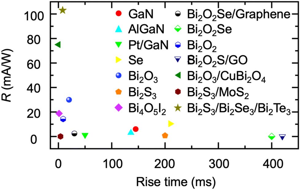 | ||
| Fig. 12 Comparison of the photodetection performance of bismuth-based semiconductors and other well investigated PEC-type photodetectors. | ||
| Sample | Fabrication method | Electrolyte | Light (nm) | Voltage (V) | R (mA W−1) | D* (Jones) | τ r/τd (ms) | Ref. |
|---|---|---|---|---|---|---|---|---|
| Bi2O3 | Drop-casting | Polysulfide | 365 | 0 | 29.92 | 7.46 × 10¹⁰ | 20/70 | 224 |
| Template-assisted | Iodine electrolyte | 365 | 0 | 1.01 | 7.79 × 10¹⁰ | 28/40 | 217 | |
| Bi2S3 | Liquid-phase exfoliation | 0.1 M KOH | 365 | 0.6 | 0.7 | 3.75 × 10⁸ | 200/200 | 218 |
| BiOI | Mist CVD | 0.5 M Na2SO4 with 0.5 M Na2SO3 | 420 | 0 | 78.33 | 4.61 × 10¹¹ | 5/90 | 79 |
| 520 | 28.89 | 1.68 × 10¹⁰ | — | |||||
| Bi2O2S | Drop-casting | 1 M KOH | 365 | 0 | 2.4 | 6.06 × 10⁹ | 30/50 | 149 |
| 0.6 | 13 | 2.34 × 10¹⁰ | 10/45 | |||||
| Coating | 0.5 M KOH | Sunlight | 0.6 | 0.23 | — | 80/70 | 147 | |
| Drop-casting | Solid-state | Sunlight | 0 | 0.0102 | — | 45/13 | 219 | |
| CBD | Iodine | 850 | 0 | 9.48 | 9.96 × 10¹⁰ | 27/47 | 221 | |
| Bi2O2Se | Drop-casting | 1 M KOH | 365 | 0 | 0.26 | 0.73 × 10⁸ | 100/140 | 222 |
| 0.6 | 0.68 | 2.44 × 10⁸ | 85/103 | |||||
| Coating | Na2SO3 | 365 | 0 | 14.24 | 3.16 × 10⁸ | 9/12 | 223 | |
| Bi2O2Se/graphene | Drop-casting | KOH/PVP | Xenon lamp | 0 | 0.0065 | — | 400/310 | 225 |
| Bi2O2S/GO | Drop-casting | KOH | Xenon lamp | 0 | 0.035 | 4.5 × 10⁸ | 420/2300 | 220 |
| Bi2S3/Bi2Se3/Bi2Te3 | CVD/PVD | 0.1 M Na2S + 0.02 M Na2SO3 | 475 | −0.1 | 103 | 8.96 × 10⁹ | 8/6.9 | 226 |
| Bi2S3/MoS2 | CVD | 0.1 M Na2SO3 | 420 | 0 | 0.218 | — | 4/15 | 227 |
| Bi2O3/CuBi2O4 | Sputtering | 0.2 M K2SO4 + 0.2 M K3PO4 + H2O2 | 380 | 0 | 75 | — | 0.18/0.19 | 228 |
Bismuth-based PEC-type photodetectors offered high photocurrent and photoresponsivity, indicating their ability to generate significant electrical signals in response to low-intensity light (Fig. 13a–c). The performance of bismuth-based PEC-type photodetectors was heavily dependent on the electrolyte composition (Fig. 13d). With the increase of electrolyte concentration, the interfacial resistance would decrease. The introduction of a hole scavenger to the electrolyte effectively promotes the separation of photogenerated electron–hole pairs, preventing the photodegradation of photoelectrodes.79 For some cases, the electrolyte may react with the bismuth-based compound, leading to corrosion, degradation, or alterations in material properties, thus compromising the stability of the device.229 Bismuth-based PEC-type photodetectors displayed fast response times, with rise and decay times in the microsecond order.79,226–228 This rapid response is essential for real-time or high-speed light sensing and optical communications. These advantages make them highly appealing for large-scale manufacturing and integration into practical devices.
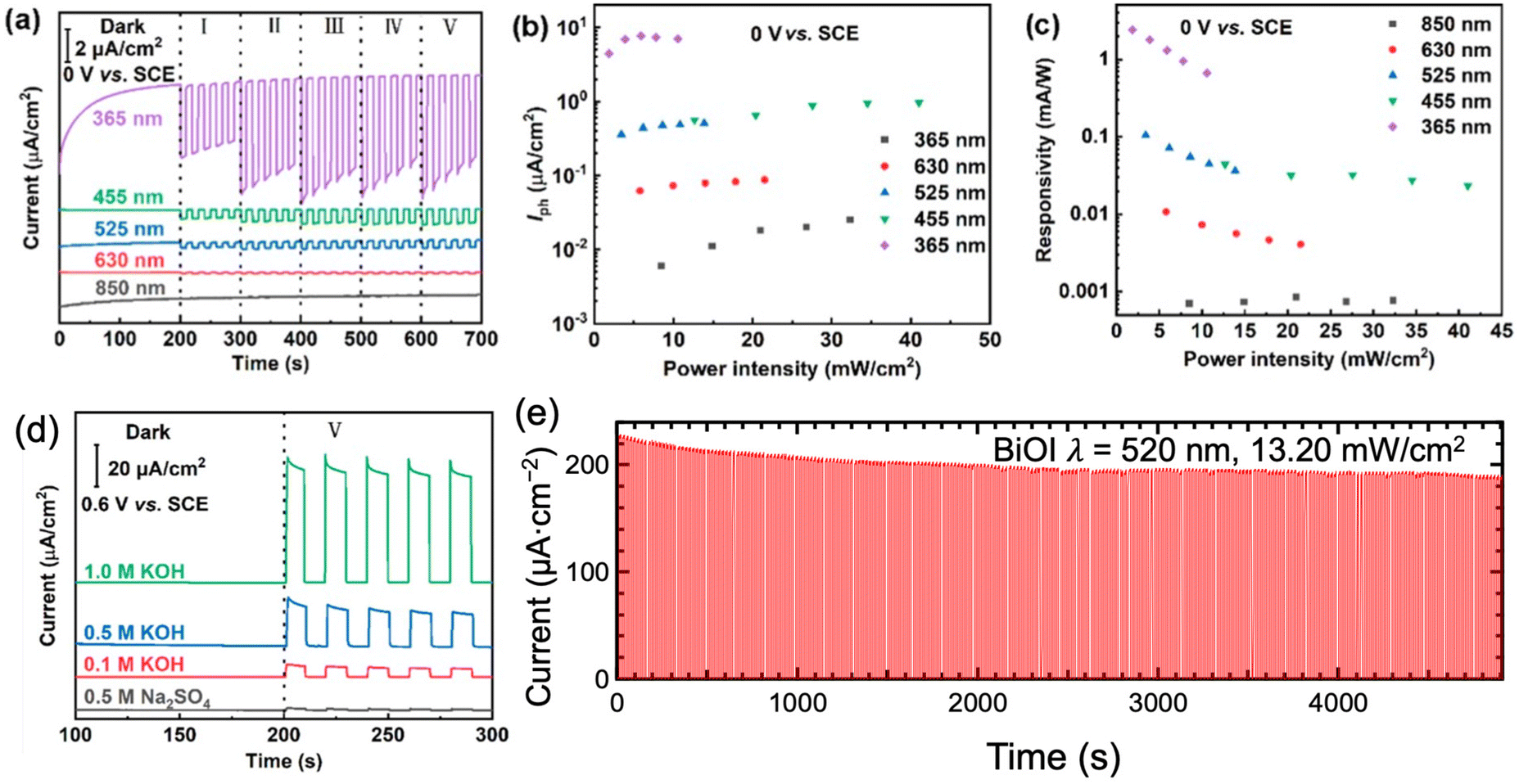 | ||
| Fig. 13 (a) Current density, (b) Iph, and (c) responsivity of Bi2O2S PEC-type photodetectors under the illumination of various wavelengths of light. (d) Effect of electrolytes on Bi2O2S PEC-type photodetectors. (e) Stability of BiOI PEC-type photodetectors. These figures have been adapted/reproduced from ref. 149 with permission from the American Chemical Society, copyright 2022 and from ref. 229 with permission from the American Chemical Society, copyright 2023. | ||
While bismuth-based compounds PEC-type photodetectors exhibited high responsivity, a broad-band range, and a rapid response time, the photoresponse stability deserved attention. To enhance the photoresponse stability, choosing a suitable electrolyte or applying a bias voltage is necessary.79,149 Appling a voltage would lose the merits of self-powering so external electrics should be supplied. Adding a hole scavenger to the electrolyte or choosing a high-conductivity electrolyte can effectively improve the PEC-type photodetection stability, where the photogenerated holes can be promptly consumed by the hole scavenger.79 However, with the increase in working time, the consumption would decrease the PEC photodetection performance.
The instability of bismuth-based compounds in the electrolyte is a major factor affecting the stability of PEC-type photodetectors. Bismuth-based compounds undergo chemical reactions when exposed to harsh environmental conditions or prolonged light illumination, leading to degradation.230 Additionally, uncontrolled charge carrier recombination at the surface or within the bismuth-based material can contribute to the deterioration of performance and stability in PEC-type photodetectors. This recombination process results in the loss of photoexcited charges before they can contribute to the photocurrent, diminishing the device's stability over time.7,214,215 The packaging and protection of bismuth-based PEC-type photodetectors are vital for their long-term stability. Inadequate encapsulation or exposure to environmental factors, such as moisture or oxygen, can accelerate device degradation and impair stability. Furthermore, peeling off the thin films or nanoplates can also lead to a decrease in photodetection performance. Potential chemical degradation reactions affecting the stability of these compounds will be discussed later.
Addressing these stability challenges requires a comprehensive understanding and control over the material structure, device construction, and environmental conditions. Ongoing research should focus on developing strategies to mitigate these stability issues through interface engineering, material modifications, protective coatings, encapsulation techniques, and device architecture. These efforts aim to enhance the stability and durability of bismuth-based PEC-type photodetectors for practical applications in marine environments. Additionally, although the PEC performance of the bismuth-based compounds is comparable to the well-investigated compounds, there are few solar-blind photodetectors for the bismuth-based semiconductors, like GaN, which might be attributed to the relatively narrow bandgap.
4.2 PEC water splitting for H2 generation
PEC water splitting is a kind of environmentally friendly, sustainable, and renewable technology to produce hydrogen energy. PEC water splitting in the sea holds significant importance from several aspects.4,5 By harnessing the abundant solar energy available in marine environments, PEC water splitting can contribute to the production of clean hydrogen, benefiting both the marine industry and the broader energy sector. Meanwhile, PEC water splitting in the sea can contribute to reducing greenhouse gas emissions and marine pollution.4,5 At present, PEC water splitting for H2 generation in the sea mainly focuses on the following aspects:2 (1) finding suitable sunlight absorption materials, and (2) optimization of the architecture of the photoelectrodes. By optimizing the configuration of the whole reaction system, including the optimization of the electrodes, the PEC performances can be much improved.Currently, bismuth binary and mixed-anion compounds possess a high enough band level for H2 (or O2) production and a narrow band gap (<3.0 eV) for efficient visible light absorption.13–15,20,24 It is indicated that the bismuth-based compounds discussed in this review showed great potential applications in H2 generation, while there are no realistic applications.13–15,20,24 Thus, this part just introduces PEC water splitting from the angle of laboratory experiments. For the bismuth binary and mixed-anion compounds in this review, most of them are n-type semiconductors. When the n-type bismuth-based semiconductor absorbed photons with energies higher than its own bandgap,25,26 the photogenerated electrons moved to a counterelectrode, like Pt, used for the H2 generation. Meanwhile, the holes migrate to the surface of the bismuth-based semiconductor and oxidize water to form O2. To promote the efficient separation and transfer of the photogenerated carriers, an external electrical or chemical potential would be necessary to reduce the resistance at the electrode interfaces and within the solution. However, relying on a large external bias would result in high energy consumption.
Table 6 comprehensively summarized the recent PEC performance for the bare bismuth binary and mixed-anion compounds photoelectrodes. It can be summarized that the crystallinity, surface morphology, crystallographic orientation, and thickness would determine the PEC performance of bismuth-based semiconductor photoelectrodes. β-Bi2O3 thin film photoanodes with nanoporous surfaces showed better PEC activity at a bias of 0.197 V VNHE than film photoanodes with dense surfaces.157 Due to the nanoporous surface, the incident light reflected between the grains and electrolyte on the surface, rather than directly passing through the film, which significantly enhanced the photon absorption ability. However, to some extent, the very rough surface morphology would cause the recombination of electron holes at the boundary of the nanoplates.231 However, it should be noted the relatively large bandgap for β-Bi2O3 was not efficient in absorbing the sunlight, leading to a moderate PEC performance among the bismuth binary and mixed-anion compounds.
| Sample | Format | Fabrication method | Bias voltage | Photocurrent density (μA cm−2) | Electrolyte | Light source | Ref. |
|---|---|---|---|---|---|---|---|
| Bi2O3 | Thin film | Coating | 1.23 V vs. RHE | 1500 | 1 M Na2SO3 | 100 mW cm−2 Xe lamp | 232 |
| CBD | 1.23 V vs. RHE | 480 | K2SO4 | 100 mW cm−2 Xe lamp | 233 | ||
| Electrochemical deposition | 0.5 V vs. Ag/AgCl | 970 | 1 M KOH | 100 mW cm−2 Xe lamp | 234 | ||
| Electrochemical deposition | 0.5 V vs. Ag/AgCl | 1000 | 0.5 M Na2SO4 | 100 mW cm−2 Xe lamp | 46 | ||
| Chemical bath deposition | 0.8 V vs. Ag/AgCl | 300 | 0.1 M Na2SO4 | 35 mW cm−2 Xe lamp | 235 | ||
| Bi2S3 | Nanosheet | Sputtering | 1 V vs. Ag/AgCl | 83 | 0.2 mol L−1 Na2SO4 | 100 W Xe lamp | 179 |
| Thin film | Coating | 1.23 V vs. RHE | 2500 | 0.1 mol L−1 Na2S and 0.1 mol L−1 Na2SO3 | 100 mW cm−2 Xe lamp | 56 | |
| Spin coating | 0.3 V vs. Ag/AgCl | 520 | 0.1 mol L−1 Na2SO3 | 50 mW cm−2 Xe lamp | 184 | ||
| Chemical bath deposition | 0 V vs. Ag/AgCl | 125 | Iodolyte AN-50 | 100 mW cm−2 Xe lamp | 236 | ||
| SILAR | 0.1 V vs. SCE | 800 | 0.1 mol L−1 Na2S | 30 mW cm−2 Xe lamp | 237 | ||
| Electrochemical deposition | 1.23 V vs. RHE | 9300 | 0.5 mol L−1 Na2S | 100 mW cm−2 Xe lamp | 183 | ||
| Mist CVD | 0.6 V vs. Ag/AgCl | 2600 | 0.5 mol L−1 Na2SO3 | 30 mW cm−2 420 nm LED light | 181 | ||
| BiOCl | Thin film | Dip-coating | 0 V | 0.05 | 0.1 mol L−1 Na2SO4 | 500 W Xe lamp | 135 |
| Spin-coating | 0 V | 0.4 | 0.1 mol L−1 Na2SO4 | 300 W Xe lamp | 238 | ||
| Mist CVD | −0.6 V vs. Ag/AgCl | 2300 | 0.5 M Na2SO4 with 0.5 M Na2SO3 | 15.2 mW cm−2 365 nm | 195 | ||
| BiOBr | Thin film | AACVD | 1 V vs. Ag/AgCl | 380 | 0.5 M Na2SO4 | 35 mW cm−2 Xe lamp | 76 |
| Electrodeposition | 0.2 V vs. RHE | 200 | 0.5 M Na2SO4 + 50 mM KBr + 20 mM Br2 | 375 W Hg quartz lamp | 239 | ||
| Mist CVD | 0.6 V vs. Ag/AgCl | 330 | 0.5 M Na2SO4 | 50 mW cm−2 420 nm | 196 | ||
| CBD | 0.9 V vs. Ag/AgCl | 70 | 0.1 M Na2SO4 | 500 W Xe lamp | 240 | ||
| BiOI | Nanosheets | Chemical transformation | 0.6 V vs. Ag/AgCl | 6.5 | 0.5 mol L−1 Na2SO4 | 100 mW cm−2 | 241 |
| Thin film | Solvothermal synthesis | 0 V | 10 | 0.1 mol L−1 Na2SO4 | 800 | 242 | |
| Spray pyrolysis deposition | 0.5 V | 100 | 1 mol L−1 Na2SO4 | 100 | 197 | ||
| AACVD | 0.5 V | ca. 80 | 0.5 mol L−1 Na2SO4 | 100 | 76 | ||
| (001) orientated thin film | Mist CVD | 0 V | 3 | 0.5 mol L−1 Na2SO4 | 70 | 79 | |
| 0.6 V | 110 | ||||||
| (102) orientated thin film | 0 V | 25 | |||||
| 0.6 V | 1360 | ||||||
| Bi2O2S | Thin film | Coating | 0 V | 2.5 | 0.5 M Na2SO4 | 300 W Xe lamp | 243 |
| Bi2O2Se | Nanosheet | Drop-casting | 1.2 V | 18 | 1 M Na2SO4 | 300 W Xe lamp | 151 |
For the Bi2S3, the deposition of continuous thin films is still very difficult, which limits the PEC performance. Meanwhile, the crystallinity influenced the photoresponse activity so that crystallized Bi2S3 thin films exhibited a much superior PEC performance to that of amorphous thin films.181 In addition, the substrate would influence the PEC performance, and the observed photovoltage trend of the Bi2S3 electrodes (FTO > ITO > Mo > Au) inversely correlates with the Schottky barrier height at the Bi2S3 and substrate interface. FTO forms an ohmic contact, resulting in the smallest barrier height, which leads to the largest photovoltage and photocurrent. This trend suggests that the choice of electrode material significantly impacts the performance of Bi2S3-based photovoltaic devices.183 Among the BiOX, BiOCl possessed a large bandgap higher than 3.0 eV, which is not suitable for harvesting solar light for the PEC applications.195 In addition, due to the long transfer distance of charge carriers, excessively thick films can lead to electron–hole recombination.196 As for the BiOBr and BiOI, there is a large number of reports confirming that BiOBr (Fig. 14a) exhibited better PEC performance than that of BiOI (Fig. 14b), although the BiOI possessed a stronger absorption ability for sunlight.76 According to the calculation report, the large electron and hole mass for the BiOI would degrade the transfer and separation efficiency of photogenerated carriers. Prof. Carmalt's group demonstrated a preferred growth of the BiOBr film resulting in internal electric fields that minimized charge carrier recombination.76 Recently, the effect of the crystallographic orientation on the PEC performance of BiOI was investigated. The intensive surface band bending and larger donor density for (102)-oriented BiOI effectively enhanced the charge separation and transfer.79 However, as for the detailed mechanism, further investigation is necessary. Unlike other compounds, the investigation of Bi2O2S and Bi2O2Se in PEC water splitting is still at the early stage, which might be attributed to the immature thin films’ deposition techniques. However, due to the narrower bandgap and high carrier mobility, it should exhibit a much more promising PEC performance.
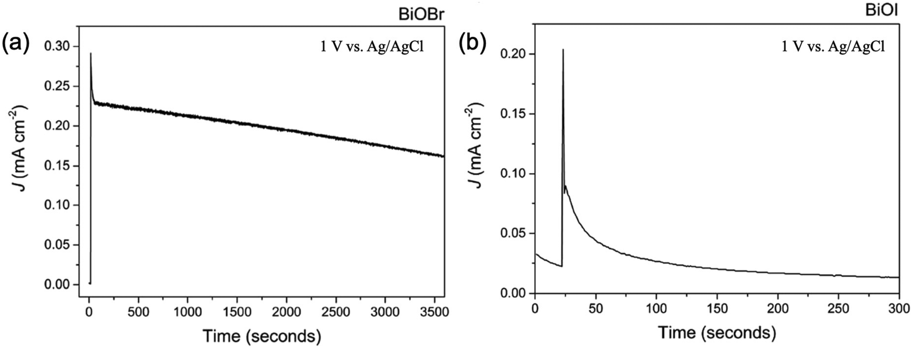 | ||
| Fig. 14 The PEC stability of the (a) BiOBr and (b) BiOI thin film under illumination.76 This figure was adapted from ref. 76 with permission from the Royal Society of Chemistry, copyright 2016. | ||
Developing effective strategies to suppress electrode degradation, such as surface passivation or introducing appropriate heterojunctions, is essential for achieving high PEC performance. Efficient and durable catalysts are required on the surface of bismuth-based photoelectrodes to facilitate the water-splitting reactions. Although there are some reports on the heterostructure construction, doping, and modification of bismuth-based photoelectrodes, this review did not comment on this point in detail. However, nearly all the reports are on the format of nanoparticles.13,14 As introduced in the above section, constructing photoelectrodes from nanoparticles via spin or dip coating is not an ideal method. Thus, exploring cost-effective synthesis methods and scalable manufacturing techniques is crucial to enable the widespread adoption of bismuth-based PEC devices.
In addition, the integration of “tandem” systems is a kind of promising strategy for enhancing PEC performance.244 In a tandem configuration, one system includes a photoelectrode paired with a solar cell that provides the necessary external bias between the photoelectrode and the counterelectrode. The other system comprises an n-type semiconductor electrode alongside a suitable p-type semiconductor electrode. At the same time, these kinds of tandem device would also broaden the light absorption range. Very recently, BiVO4–BiOI-based photoelectrodes exhibited a comparable PEC performance to that of the well-investigated photoelectrodes,244 indicating the potential of bismuth-based semiconductors in PEC water splitting. Although the bismuth-based semiconductors did not exhibit much promising performance like other well-investigated compounds like Cu2O and TiO2, under continuous efforts from the point of innovative material design and advanced fabrication techniques, it is possible to realize the full potential of bismuth-based photoelectrodes in PEC applications.
3.3 Challenges and issues for PEC applications
PEC-type photodetection and water splitting based on bismuth binary and mixed-anion compounds showed promising potential in marine engineering. However, since 1990, the stability of bismuth-based compounds in electrolytes has attracted the attention of researchers.245 Understanding the degradation mechanisms of bismuth-based photoelectrodes is critical for enhancing their stability and durability in PEC-type applications.One degradation mechanism is photocorrosion, where electrochemical reactions occurred within the material under light illumination, leading to its deterioration. Photocorrosion involves reduction, dissolution, or the formation of self-passivating surface layers.197 Additionally, bismuth-based photoelectrodes undergo surface oxidation in the presence of oxygen or water.197 Another factor contributing to degradation is rapid electron–hole recombination within the bismuth-based material. This recombination process hampers the charge separation efficiency, resulting in a reduced photocurrent and overall photoelectrode performance.76 Previous reports suggest that changing the electrolytes, with or without hole scavengers like Na2SO3, simplifies the degradation mechanism.195 If electrons cannot be promptly consumed, photogenerated electrons may reduce Bi3+ into Bi (0) following the equation:
| BiOX + 2H+ + 3e− → Bi + X− + H2O |
5. Prospects and outlook of recent advances
5.1 Optimization of electrode architecture
To some extent, bismuth binary and mixed-anion compounds for PEC-type device construction were underexplored for a long time owing to the not good stability. Very recently, Andrei and coworkers confirmed that bismuth-based semiconductor BiOl–BiVO4 tandem photoelectrodes can approach and even challenge the performance of well-established light absorbers with an appropriate device architecture.244 In this work, the p-type amorphous NiOx and n-type ZnO were used as a hole transport and electron layer respectively, and graphite composite epoxy was used as a conductive encapsulator to improve the transfer and separation efficiency of photogenerated electron–hole pairs. In addition, multiple-pixel devices were found that would be useful in overcoming the current leakage in the grain boundary and defects of thin films.244In addition, Feng proposed the planar interdigital photoelectrode structure (Fig. 15), which has been successfully applied in p-Se and CuSe PEC-type photodetectors, showing various advantages, like a simplified design and excellent photoresponse.246 The planar interdigital photoelectrode structure offers a novel approach to the development of high-performance, cost-effective, photoelectrodes.246 Shortly, further optimization of the lateral and vertical structure would be necessary for the enhancement of the PEC performance of conventional PEC-type devices.
 | ||
| Fig. 15 Setup of the planar interdigital photoelectrodes.246 This figure was adapted from ref. 246 with permission from Wiley, copyright 2024. | ||
5.2 Fabrication of freestanding membranes
Freestanding membranes, also known as self-supporting membranes, are thin, flexible structures or films that are capable of standing or existing independently without the need for additional external support.247 Freestanding membranes are typically thin and flexible, allowing them to conform to different shapes and surfaces. This flexibility enables their integration into complex structures or devices, making them suitable for applications that require conformable materials. Meanwhile, the freestanding membranes are free of solid-state bulk substrates like single crystal and glass substrates, which effectively reduce the cost and weight.248 Importantly, freestanding membranes minimize interfacial effects between the membrane and the supporting substrate. This allows for a more accurate characterization of intrinsic membrane properties and mitigates potential limitations associated with interfacial interactions, such as diffusion barriers or catalytic effects.249,250Currently, there are nearly no reports on bismuth-based binary and mixed-anion compound freestanding membranes, while there are several reports on the exfoliation and transfer of Bi2O2Se nanoplates.208,209 Thus, future research should be devoted to the perspective of selecting suitable substrates, and optimization of exploitation-transfer techniques. Coupling the freestanding membranes with flexible organic conduction layers will be suitable for practical PEC device construction with low cost and weight, better flexibility, and enhanced PEC performance. In addition, the successful fabrication of freestanding membranes would promote the investigation of intrinsic properties and enhancement of transfer and separation efficiency of photogenerated electron–hole pairs. Advances in material science and manufacturing techniques should continue to expand the capabilities and explore new applications for freestanding membranes. Freestanding membranes offer a versatile platform for various applications like flexible smart devices.
5.3 Underwater communication through PEC-type photodetectors
PEC-type photodetectors can play a crucial role in underwater communication systems by enabling the wireless transmission of data using light.7 PEC-type photodetectors excel at detecting light signals and converting them into electrical signals. In wireless communication, these devices can receive optical signals carrying information and convert them into electrical signals that can be processed by electronic systems. PEC-type photodetectors can be integrated into optical communication systems to receive data encoded in optical signals (Fig. 16).216 For instance, in free-space optical communication or optical wireless communication, PEC-type photodetectors can detect modulated light signals, such as those from laser diodes or light-emitting diodes (LEDs), and convert them into electrical signals for further processing. As depicted in section 4.1, the PEC-type photodetectors constructed from the bismuth binary and mixed-anion compounds can operate with self-powered, high-photoresponse speeds, excellent sensitivity, and a broad photoresponse to light signals, making them suitable for applications such as wireless communication links between remote locations, the transmission of data at high speeds, and supporting a large data transfer capacity.216 However, the development of PEC-type photodetectors in the field of underwater communication is still at an early stage. Shortly, the PEC-type photodetectors can be paired with other electronic and optical components, like optical transmitters, to establish a complete wireless underwater communication link, allowing for bidirectional communication.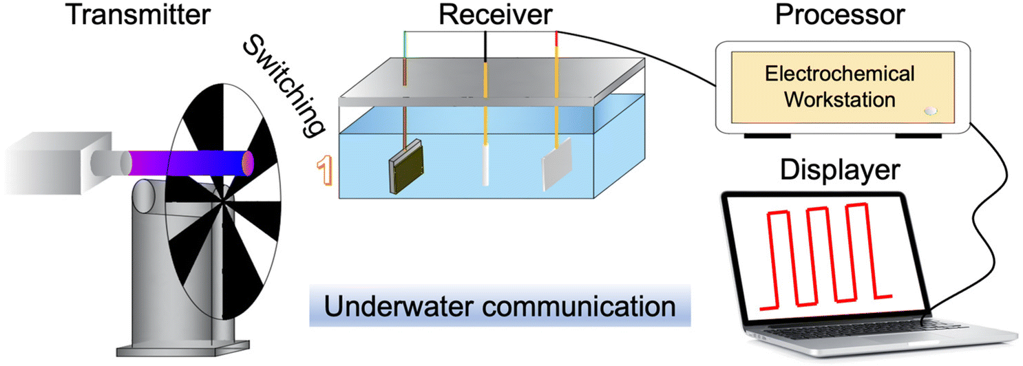 | ||
| Fig. 16 The schematic diagram for the underwater optical communication system.216 This figure was adapted with permission from Wiley, copyright 2024. | ||
5.4 Finding novel mixed-anion compounds
Bismuth-based binary and mixed-anion compounds have been regarded as a kind of important functional material due to their various extraordinary properties, like the tunable bandgap and ultrahigh carrier mobility.251 In the past decades, the investigation of bismuth-based binary and mixed-anion compounds was mainly focused on simple ternary compounds like bismuth oxyhalides,14 though slightly changing the chemical composition would bring unprecedented properties. For instance, despite the similar Bi:S molar ratio and crystal structure for Bi2S3 and Bi13S18I2, the bandgap of Bi13S18I2 (0.8 eV)252 was much narrower than that of Bi2S3 (1.3 eV).181 Benefiting from the narrow bandgap, Bi13S18I2 attracted much attention for various applications, like solar cells, photoelectrodes, and photodetectors.253–255 Thus, for fruitful applications of bismuth-based binary and mixed-anion compounds, controlling the anion composition would be a promising way to optimize the physical and chemical properties of bismuth-based compounds to meet the high demand of PEC-type device construction.
In addition, doping elements, introducing oxygen vacancies, and constructing heterostructures can significantly enhance the PEC performance of bismuth-based compounds.256 Most of the previously published reports on bismuth-based compounds have focused on nanoparticles. Achieving modifications in the format of thin films remains challenging, and this can be attributed to the immaturity of deposition techniques for thin film fabrication. Despite these challenges, the modification of bismuth-based compounds holds promise for improving their properties and expanding their potential applications in PEC systems. Efforts in research and development are necessary to overcome the current limitations and fully unlock the potential of bismuth-based compounds. Progress in materials synthesis techniques, especially in developing reliable methods for thin film deposition, will be essential to advance the modification of bismuth-based compounds for practical applications. Continued research is vital to address these challenges and achieve the desired improvements in the properties and performance of bismuth-based compounds.
5.5 Challenges for practical applications in marine engineering
PEC-type devices based on bismuth-based compounds hold great potential for practical applications in marine engineering. However, there are several challenges associated with PEC activities in marine environments. One of the main challenges is corrosion. Marine environments are highly corrosive due to the presence of salts, minerals, and other impurities in seawater. Therefore, PEC materials and electrodes used in water splitting systems must be corrosion-resistant to ensure long-term performance and durability. Another challenge is fouling. Marine environments are prone to fouling, where organisms such as algae, barnacles, and mussels attach and grow on the surfaces of PEC systems. This can hinder water flow and reduce the efficiency of light absorption, leading to decreased performance and increased maintenance requirements. Moreover, seawater has higher light absorption and scattering properties compared with freshwater or air, which can further reduce the efficiency of light absorption in PEC systems. As mentioned above, the stability and durability of bismuth-based materials in marine environments are also crucial for their practical applications. Research and development efforts are required to improve the stability and durability of these materials under marine conditions. Lastly, the manufacturing, installation, and maintenance of large-scale PEC systems in marine environments require significant investments and infrastructure. Future research should focus on improving the corrosion resistance, anti-fouling properties, light absorption, stability, and cost-effectiveness of PEC materials and systems in marine engineering applications.6. Conclusion
This review initially discusses the crystal structure and intrinsic properties of bismuth binary and mixed-anion compounds. Their excellent optical and electrical properties make them promising candidates for potential applications in marine environments. Currently, PEC-type devices based on bismuth binary and mixed-anion compounds can effectively harness photon energy and perform various functions in marine engineering, such as hydrogen production and photodetection. However, it is important to recognize that further research and development are required to optimize the performance and stability of bismuth-based PEC devices for marine engineering applications. While the application of bismuth optoelectronic semiconductor materials in marine engineering is still in the research stage, the deepening exploration of marine spaces will unveil the unique advantages of bismuth-based semiconductor materials in multiple scenarios, including underwater communication, desalination and water treatment, corrosion protection, and environmental monitoring. Meanwhile, these materials can contribute to realize the zero carbon and smart ocean.Author contributions
Jiaji Zhang and Zaichun Sun conceived this review. All authors did the literature survey, wrote the manuscript, and commented on the paper. All authors have approved the final version of this manuscript.Conflicts of interest
The authors declare no competing financial interests.Acknowledgements
This work was supported by the National Natural Science Foundation of China (No. 52272161), Key R&D Project of Hainan Yourui Cohesion Technology Co., Ltd (20231201ZZKY002), Wuhan Key R&D Plan (2023020402010590), and Fundamental Research Funds for the Central Universities (WUT: 2024IVA007). We thank Mr Yao Chen, Guoxiao Zhao, Qinna Ren, and Weibojie Lu for their assistance in the literature survey.References
- R. Tang, S. Zhou, Z. Zhang, R. Zheng and J. Huang, Adv. Mater., 2021, 33, 2005389 CrossRef CAS PubMed.
- A. Vilanova, P. Dias, T. Lopes and A. Mendes, Chem. Soc. Rev., 2024, 53, 2388–2434 RSC.
- C. S. Gopinath and N. Nalajala, J. Mater. Chem. A, 2021, 9, 1353–1371 RSC.
- X. Zeng, Y. Liu, X. Hu and X. Zhang, Green Chem., 2021, 23, 1466–1494 RSC.
- N. S. Lewis, Science, 2016, 351, 353 CrossRef CAS PubMed.
- Y. Ding, S. Maitra, C. Wang, S. Halder, R. Zheng, T. Barakat, S. Roy, L. Chen and B. Su, Interdiscip. Mater., 2022, 1, 213–255 CrossRef CAS.
- H. Qiao, Z. Huang, X. Ren, S. Liu, Y. Zhang, X. Qi and H. Zhang, Adv. Opt. Mater., 2020, 8, 1900765 CrossRef CAS.
- J. Gao, X. Yao, Y. Chen, Z. Gao and J. Zhang, Anal. Chem., 2021, 93, 677–682 CrossRef CAS PubMed.
- K. Fujishima and A. Honda, Nature, 1972, 238, 38–40 CrossRef PubMed.
- C. Ros, T. Andreu and J. R. Morante, J. Mater. Chem. A, 2020, 8, 10625–10669 RSC.
- R. Siavash Moakhar, S. M. Hosseini-Hosseinabad, S. Masudy-Panah, A. Seza, M. Jalali, H. Fallah-Arani, F. Dabir, S. Gholipour, Y. Abdi, M. Bagheri-Hariri, N. Riahi-Noori, Y. F. Lim, A. Hagfeldt and M. Saliba, Adv. Mater., 2021, 33, 2007285 CrossRef CAS PubMed.
- R. Gao and D. Yan, Adv. Energy Mater., 2020, 10, 1900954 CrossRef CAS.
- S. Wang, L. Wang and W. Huang, J. Mater. Chem. A, 2020, 8, 24307–24352 RSC.
- X. Wu, C. Y. Toe, C. Su, Y. H. Ng, R. Amal and J. Scott, J. Mater. Chem. A, 2020, 8, 15302–15318 RSC.
- A. Zhao, L. Zhang, Y. Guo, H. Li, S. Ruan and Y. J. Zeng, 2D Mater., 2021, 8, 012004 CrossRef CAS.
- K. Hoshi and Y. Mizuguchi, J. Phys.: Condens. Matter, 2021, 33, 473001 CrossRef CAS PubMed.
- J. He, X. Hu, Z. Liu, W. Chen and G. Longo, Adv. Funct. Mater., 2023, 33, 2306075 CrossRef CAS.
- R. Mohan, Nat. Chem., 2010, 2, 336 CrossRef CAS PubMed.
- A. Walsh, D. J. Payne, R. G. Egdell and G. W. Watson, Chem. Soc. Rev., 2011, 40, 4455–4463 RSC.
- X. Meng and Z. Zhang, J. Mol. Catal. A: Chem., 2016, 423, 533–549 CrossRef CAS.
- J. Di, J. Xia, H. Li, S. Guo and S. Dai, Nano Energy, 2017, 41, 172–192 CrossRef CAS.
- N. C. Miller and M. Bernechea, APL Mater., 2018, 6, 084503 CrossRef CAS.
- P. Xia, Y. J. Song, Y. Z. Liu, M. X. Long, C. Yang, X. Y. Zhang and T. Zhang, J. Mater. Chem. C, 2023, 12, 1609–1624 RSC.
- L. Ye, Y. Deng, L. Wang, H. Xie and F. Su, ChemSusChem, 2019, 12, 3671–3701 CrossRef CAS PubMed.
- Z. Ran, X. Wang, Y. Li, D. Yang, X. G. Zhao, K. Biswas, D. J. Singh and L. Zhang, npj Comput. Mater., 2018, 4, 1–7 CrossRef CAS.
- E. Wlaźlak, A. Blachecki, M. Bisztyga-Szklarz, S. Klejna, T. Mazur, K. Mech, K. Pilarczyk, D. Przyczyna, M. Suchecki, P. Zawal and K. Szaciłowski, Chem. Commun., 2018, 54, 12133–12162 RSC.
- J. Wu, H. Yuan, M. Meng, C. Chen, Y. Sun, Z. Chen, W. Dang, C. Tan, Y. Liu, J. Yin, Y. Zhou, S. Huang, H. Q. Xu, Y. Cui, H. Y. Hwang, Z. Liu, Y. Chen, B. Yan and H. Peng, Nat. Nanotechnol., 2017, 12, 530–534 CrossRef CAS PubMed.
- R. L. Z. Hoye, L. C. Lee, R. C. Kurchin, T. N. Huq, K. H. L. Zhang, M. Sponseller, L. Nienhaus, R. E. Brandt, J. Jean, J. A. Polizzotti, A. Kursumović, M. G. Bawendi, V. Bulović, V. Stevanović, T. Buonassisi and J. L. MacManus-Driscoll, Adv. Mater., 2017, 29, 1702176 CrossRef PubMed.
- M. Wu, Z. Lou, C. M. Dai, T. Wang, J. Wang, Z. Zhu, Z. Xu, T. Sun, W. Li, X. Zheng and X. Lin, Adv. Mater., 2023, 35, 2300450 CrossRef CAS PubMed.
- T. Ghosh, M. Samanta, A. Vasdev, K. Dolui, J. Ghatak, T. Das, G. Sheet and K. Biswas, Nano Lett., 2019, 19, 5703–5709 CrossRef CAS PubMed.
- S. Abhirami, E. P. Amaladass, S. Amirthapandian, C. David and A. Mani, Phys. Chem. Chem. Phys., 2023, 26, 2745–2767 Search PubMed.
- M. Channegowda, R. Mulla, Y. Nagaraj, S. Lokesh, S. Nayak, S. Mudhulu, C. K. Rastogi, C. W. Dunnill, H. K. Rajan and A. Khosla, ACS Appl. Energy Mater., 2022, 5, 7913–7943 CrossRef CAS.
- C. Yang, Y. Zhao, P. Liu, D. Wang, Y. Sun, C. Li, Y. Dong, M. Ye, N. Zhang, Z. Zhu, H. Jiang, J. Zhu, M. Shuai, T. Wei and Y. Zhao, Cryst. Res. Technol., 2023, 58, 2300081 CrossRef CAS.
- M. Sahu and C. Park, Mater. Today Sustain., 2023, 23, 100441 CrossRef.
- X. Wang, B. Liu, Y. Zhang, T. Butburee, K. (Ken) Ostrikov, S. Wang and W. Huang, EcoEnergy, 2023, 1, 108–153 CrossRef.
- Y. Zhang, L. Xu, B. Liu, X. Wang, T. Wang, X. Xiao, S. Wang and W. Huang, ACS Catal., 2023, 13, 5938–5948 CrossRef CAS.
- S. Wang, T. He, J. H. Yun, Y. Hu, M. Xiao, A. Du and L. Wang, Adv. Funct. Mater., 2018, 28, 1802685 CrossRef.
- B. Guan, J. Chen, Z. Li, Z. Zhuang, Y. Chen, Z. Ma, J. Guo, C. Zhu, X. Hu, S. Zhao, H. Dang, L. Chen, K. Shu, Z. Guo, K. Shi, Y. Li, C. Yi, J. Hu and Z. Huang, Energy Fuels, 2024, 38, 806–853 CrossRef CAS.
- S. Wang, X. Wang, B. Liu, Z. Guo, K. Ostrikov, L. Wang and W. Huang, Nanoscale, 2021, 13, 17989–18009 RSC.
- A. H. Zahid and Q. Han, Nanoscale, 2021, 13, 17687–17724 RSC.
- F. K. Wang, S. J. Yang and T. Y. Zhai, iScience, 2021, 24, 103291 CrossRef CAS PubMed.
- P. Ngabonziza, Nanotechnology, 2022, 33, 192001 CrossRef PubMed.
- X. Tang, Z. Li, W. Liu, Q. Zhang and C. Uher, Interdiscip. Mater., 2022, 1, 88–115 CrossRef CAS.
- A. J. Lovett, M. P. Wells, Z. He, J. Lu, H. Wang and J. L. Macmanus-Driscoll, J. Mater. Chem. A, 2022, 10, 3478–3484 RSC.
- D. Pérez-Mezcua, I. Bretos, R. Jiménez, J. Ricote, R. J. Jiménez-Rioboó, C. G. Da Silva, D. Chateigner, L. Fuentes-Cobas, R. Sirera and M. L. Calzada, Sci. Rep., 2016, 6, 39561 CrossRef PubMed.
- M. W. Kim, B. Joshi, E. Samuel, K. Kim, Y. Il Kim, T. G. Kim, M. T. Swihart and S. S. Yoon, J. Alloys Compd., 2018, 764, 881–889 CrossRef CAS.
- Y. Li, J. Song, Y. Ji, X. Lu, Q. Tian, J. Chen and Z. Sui, J. Phys. Chem. Solids, 2022, 163, 110562 CrossRef CAS.
- Z. Wu, M. C. Chong, S. Zhang, J. Li and Y. Zhu, Sci. China: Chem., 2024 DOI:10.1007/s11426-023-1943-5.
- B. Wu, Z. Su, Q. Wu, D. H. Kuo, P. Zhang, L. Chen, A. B. Abdeta, M. T. Mosisa, J. Lin, X. Chen and X. Liu, Mater. Today Chem., 2023, 33, 101697 CrossRef CAS.
- Z. Zhu, S. K. Iyemperumal, K. Kushnir, A. D. Carl, L. Zhou, D. R. Brodeur, R. L. Grimm, L. V. Titova, N. A. Deskins and P. M. Rao, Sustainable Energy Fuels, 2017, 1, 2134–2144 RSC.
- P. S. Sonawane and L. A. Patil, Mater. Chem. Phys., 2007, 105, 157–161 CrossRef CAS.
- Z. Hu, D. Zhao, Y. Li, X. Lv, J. Song, L. Meng, S. Y. Lien and P. Gao, ACS Mater. Lett., 2023, 5, 2987–2999 CrossRef CAS.
- M. Bernechea, Y. Cao and G. Konstantatos, J. Mater. Chem. A, 2015, 3, 20642–20648 RSC.
- M. Zargazi and M. H. Entezari, J. Hazard. Mater., 2020, 384, 121300 CrossRef CAS PubMed.
- L. Zhao, J. Zhou, L. Zhang, X. Sun, X. Sun, T. Yan, X. Ren and Q. Wei, ACS Appl. Mater. Interfaces, 2020, 12, 55838–55843 CrossRef CAS PubMed.
- P. Subramanyam, T. Vinodkumar, M. Deepa and C. Subrahmanyam, J. Mater. Chem. C, 2019, 7, 6398–6405 RSC.
- M. F. Afsar, M. A. Rafiq, A. Jamil, S. Fareed, F. Siddique, A. I. Y. Tok and M. M. U. Hasan, ACS Omega, 2019, 4, 2030–2039 CrossRef CAS PubMed.
- W. Yang, J. Yang, K. Zhao, Q. Gao, L. Liu, Z. Zhou, S. Hou, X. Wang, G. Shen, X. Pang, Q. Xu and Z. Wei, Adv. Sci., 2021, 8, 2100075 CrossRef CAS PubMed.
- Y. Hu, L. Mao, X. Yuan, J. Lu, R. Chen, T. Chen, W. Zhang, X. Xue, W. Yan, M. Shokouhimehr, X. L. Zhang and Z. Jin, Nano Res., 2020, 13, 2226–2232 CrossRef CAS.
- N. Huo, A. Figueroba, Y. Yang, S. Christodoulou, A. Stavrinadis, C. Magén and G. Konstantatos, Adv. Opt. Mater., 2019, 7, 1900258 CrossRef.
- P. Rong, S. Gao, S. Ren, H. Lu, J. Yan, L. Li, M. Zhang, Y. Han, S. Jiao and J. Wang, Adv. Funct. Mater., 2023, 33, 2300159 CrossRef CAS.
- Y. Zhao, L. Ma, Y. Zhu, P. Qin, H. Li, F. Mo, D. Wang, G. Liang, Q. Yang, W. Liu and C. Zhi, ACS Nano, 2019, 13, 7270–7280 CrossRef CAS PubMed.
- B. Long, Z. Qiao, J. Zhang, S. Zhang, M. S. Balogun, J. Lu, S. Song and Y. Tong, J. Mater. Chem. A, 2019, 7, 11370–11378 RSC.
- J. Jiang, X. Che, Y. Qian, L. Wang, Y. Zhang and Z. Wang, Front. Mater., 2020, 7, 234 CrossRef.
- J. Guo, J. Yang, Z. Ge, B. Jiang, Y. Qiu, Y. Zhu and X. Wang, Adv. Funct. Mater., 2021, 12, 202102838 Search PubMed.
- S. Sharma, H. H. Singh, S. Kumar and N. Khare, Nanotechnology, 2021, 32, 335705 CrossRef CAS.
- J. Yang, Y. Xue, C. Han, X. Zhang, K. Sa, J. Jia, H. Ye and Y. Liang, Catal. Sci. Technol., 2023, 13, 5313–5325 RSC.
- X. D. Dong, Y. M. Zhang and Z. Y. Zhao, Inorg. Chem., 2021, 60, 8461–8474 CrossRef CAS PubMed.
- S. Rieger, T. Fürmann, J. K. Stolarczyk and J. Feldmann, Nano Lett., 2021, 21, 7887–7893 CrossRef CAS PubMed.
- T. Li, X. Zhang, C. Zhang, R. Li, J. Liu, R. Lv, H. Zhang, P. Han, C. Fan and Z. Zheng, Phys. Chem. Chem. Phys., 2019, 21, 868–875 RSC.
- D. Kato, K. Hongo, R. Maezono, M. Higashi, H. Kunioku, M. Yabuuchi, H. Suzuki, H. Okajima, C. Zhong, K. Nakano, R. Abe and H. Kageyama, J. Am. Chem. Soc., 2017, 139, 18725–18731 CrossRef CAS PubMed.
- L. S. Gómez-Velázquez, A. Hernández-Gordillo, M. J. Robinson, V. J. Leppert, S. E. Rodil and M. Bizarro, Dalton Trans., 2018, 47, 12459–12467 RSC.
- A. M. Ganose, M. Cuff, K. T. Butler, A. Walsh and D. O. Scanlon, Chem. Mater., 2016, 28, 1980–1984 CrossRef CAS PubMed.
- W. L. Huang and Q. Zhu, Comput. Mater. Sci., 2009, 46, 1076–1084 CrossRef CAS.
- H. Zhang, L. Liu and Z. Zhou, RSC Adv., 2012, 2, 9224–9229 RSC.
- D. S. Bhachu, S. J. A. Moniz, S. Sathasivam, D. O. Scanlon, A. Walsh, S. M. Bawaked, M. Mokhtar, A. Y. Obaid, I. P. Parkin, J. Tang and C. J. Carmalt, Chem. Sci., 2016, 7, 4832–4841 RSC.
- R. A. Jagt, T. N. Huq, K. M. Börsig, D. Sauven, L. C. Lee, J. L. Macmanus-Driscoll and R. L. Z. Hoye, J. Mater. Chem. C, 2020, 8, 10791–10797 RSC.
- M. Shi, G. Li, J. Li, X. Jin, X. Tao, B. Zeng, E. A. Pidko, R. Li and C. Li, Angew. Chem., Int. Ed., 2020, 59, 6590–6595 CrossRef CAS PubMed.
- Z. Sun, H. Zhang and B. Mei, Inorg. Chem., 2023, 62, 5512–5519 CrossRef CAS PubMed.
- W. Zeng, J. Li, L. Feng, H. Pan, X. Zhang, H. Sun and Z. Liu, Adv. Funct. Mater., 2019, 29, 1900129 CrossRef.
- B. S. Defects, T. N. Huq, L. C. Lee, L. Eyre, W. Li, R. A. Jagt, C. Kim, S. Fearn, V. Pecunia, F. Deschler, J. L. Macmanus-driscoll and R. L. Z. Hoye, Adv. Funct. Mater., 2020, 11, 1909983 Search PubMed.
- R. A. Jagt, I. Bravić, L. Eyre, K. Gałkowski, J. Borowiec, K. R. Dudipala, M. Baranowski, M. Dyksik, T. W. J. van de Goor, T. Kreouzis, M. Xiao, A. Bevan, P. Płochocka, S. D. Stranks, F. Deschler, B. Monserrat, J. L. MacManus-Driscoll and R. L. Z. Hoye, Nat. Commun., 2023, 14, 1–12 Search PubMed.
- C. Gong, J. Chu, S. Qian, C. Yin, X. Hu, H. Wang, Y. Wang, X. Ding, S. Jiang, A. Li, Y. Gong, X. Wang, C. Li, T. Zhai and J. Xiong, Adv. Mater., 2020, 32, 1908242 CrossRef CAS PubMed.
- C. Wang, C. Hu, F. Chen, H. Li, Y. Zhang, T. Ma and H. Huang, Adv. Funct. Mater., 2023, 33, 2301144 CrossRef CAS.
- P. Lei, H. Duan, L. Qin, X. Wei, R. Tao, Z. Wang, F. Guo, M. Song, W. Jie and J. Hao, Adv. Funct. Mater., 2022, 32, 2201276 CrossRef CAS.
- T. Li and H. Peng, Acc. Mater. Res., 2021, 2, 842–853 CrossRef CAS.
- M. Wu and X. C. Zeng, Nano Lett., 2017, 17, 6309–6314 CrossRef CAS PubMed.
- Y. Sun, J. Zhang, S. Ye, J. Song and J. Qu, Adv. Funct. Mater., 2020, 30, 2004480 CrossRef CAS.
- F. Wang, S. Yang, J. Wu, X. Hu, Y. Li, H. Li, X. Liu, J. Luo and T. Zhai, InfoMat, 2021, 3, 1251–1271 CrossRef CAS.
- Y. Liang, X. Zhou, W. Li and H. Peng, APL Mater., 2021, 9, 060905 CrossRef CAS.
- J. Wu, C. Qiu, H. Fu, S. Chen, C. Zhang, Z. Dou, C. Tan, T. Tu, T. Li, Y. Zhang, Z. Zhang, L. M. Peng, P. Gao, B. Yan and H. Peng, Nano Lett., 2019, 19, 197–202 CrossRef CAS PubMed.
- J. Wu, H. Yuan, M. Meng, C. Chen, Y. Sun, Z. Chen, W. Dang, C. Tan, Y. Liu, J. Yin, Y. Zhou, S. Huang, H. Q. Xu, Y. Cui, H. Y. Hwang, Z. Liu, Y. Chen, B. Yan and H. Peng, Nat. Nanotechnol., 2017, 12, 530–534 CrossRef CAS PubMed.
- Z. Guan, H. Hu, X. Shen, P. Xiang, N. Zhong, J. Chu and C. Duan, Adv. Electron. Mater., 2020, 6, 1900818 CrossRef CAS.
- M. T. Hossain, T. Jena and P. K. Giri, Small Struct., 2024, 5, 2300511 CrossRef.
- H. Guo, J. Xiao, J. Qu, D. Legut and Q. Zhang, J. Phys. Chem. C, 2019, 123, 24024–24030 CrossRef CAS.
- C. W. Hu, Y. Yang, C. Hou and T. X. Liang, Mater. Today Commun., 2020, 25, 101619 CrossRef CAS.
- H. Tang, B. Shi, Y. Wang, C. Yang, S. Liu, Y. Li, R. Quhe and J. Lu, Phys. Rev. Appl., 2021, 15, 1 Search PubMed.
- Q. Wei, C. Lin, Y. Li, X. Zhang, Q. Zhang, Q. Shen, Y. Cheng and W. Huang, J. Appl. Phys., 2018, 124, 055701 CrossRef.
- T. Cheng, C. Tan, S. Zhang, T. Tu, H. Peng and Z. Liu, J. Phys. Chem. C, 2018, 122, 19970–19980 CrossRef CAS.
- H. Y. Song, X. J. Ge, M. Y. Shang, J. Zhang and J. T. Lü, Phys. Chem. Chem. Phys., 2019, 21, 18259–18264 RSC.
- C. Zhang, J. Wu, Y. Sun, C. Tan, T. Li, T. Tu, Y. Zhang, Y. Liang, X. Zhou, P. Gao and H. Peng, J. Am. Chem. Soc., 2020, 142, 2726–2731 CrossRef CAS PubMed.
- H. Tao, T. Wang, D. Li, J. Xing and G. Li, J. Semicond., 2023, 44, 031001 CrossRef.
- C. Tan, S. Xu, Z. Tan, L. Sun, J. Wu, T. Li and H. Peng, InfoMat, 2019, 1, 390–395 CrossRef CAS.
- W. Chen, R. Zhang, Y. Sun, J. Wang, Y. Fan and B. Liu, Adv. Powder Mater., 2023, 2, 100080 CrossRef.
- Y. Chen, W. Ma, C. Tan, M. Luo, W. Zhou, N. Yao, H. Wang, L. Zhang, T. Xu, T. Tong, Y. Zhou, Y. Xu, C. Yu, C. Shan, H. Peng, F. Yue, P. Wang, Z. Huang and W. Hu, Adv. Funct. Mater., 2021, 31, 202009554 Search PubMed.
- P. Luo, F. Wang, J. Qu, K. Liu, X. Hu, K. Liu and T. Zhai, Adv. Funct. Mater., 2021, 31, 202008351 Search PubMed.
- J. Li, Z. Wang, J. Chu, Z. Cheng, P. He, J. Wang, L. Yin, R. Cheng, N. Li, Y. Wen and J. He, Appl. Phys. Lett., 2019, 114, 5094192 Search PubMed.
- M. Yu, C. Fang, J. Han, W. Liu, S. Gao and K. Huang, ACS Appl. Mater. Interfaces, 2022, 14, 13507–13515 CrossRef CAS PubMed.
- H. Yang, C. Tan, C. Deng, R. Zhang, X. Zheng, X. Zhang, Y. Hu, X. Guo, G. Wang, T. Jiang, Y. Zhang, G. Peng, H. Peng, X. Zhang and S. Qin, Small, 2019, 15, 201904482 Search PubMed.
- L. Pan, X. L. Shi, C. Song, W. Di Liu, Q. Sun, C. Lu, Q. Liu, Y. Wang and Z. G. Chen, Adv. Funct. Mater., 2022, 32, 202202927 Search PubMed.
- W. Ai, J. Chen, X. Dong, Z. Gao, Y. He, Z. Liu, H. Fu, F. Luo and J. Wu, Nano Lett., 2022, 22, 7659–7666 CrossRef CAS PubMed.
- Y. Yan, Y. Xu, S. Lei, X. Ou, L. Chen, J. Xiong, Y. Xiao and B. Cheng, Dalton Trans., 2018, 47, 3408–3416 RSC.
- J. Tang, T. Zhang, Z. Duan, C. Li, C. Meng, Y. Zhang, Q. Zhang, D. Hou, Q. Xv and Y. Zhu, Chem. Phys. Lett., 2021, 768, 138354 CrossRef CAS.
- V. G. Ilves, V. S. Gaviko, A. M. Murzakaev, S. Y. Sokovnin, M. A. Uimin and M. G. Zuev, Ceram. Int., 2023, 49, 21848–21854 CrossRef CAS.
- P. Guo, F. Yin, J. Zhang, B. Chen, Z. Ni, L. Shi, M. Han, Z. Wu and G. Li, ACS Appl. Mater. Interfaces, 2024, 16, 17540–17552 CrossRef CAS PubMed.
- Y. C. Liang and K. W. Liang, CrystEngComm, 2023, 25, 5035–5049 RSC.
- Y. Lu, Y. Zhao, J. Zhao, Y. Song, Z. Huang, F. Gao, N. Li and Y. Li, Cryst. Growth Des., 2015, 15, 1031–1042 CrossRef CAS.
- M. Weber, M. Schlesinger and M. Mehring, Cryst. Growth Des., 2016, 16, 5678–5688 CrossRef CAS.
- T. Selvamani, S. Anandan, L. Granone, D. W. Bahnemann and M. Ashokkumar, Mater. Chem. Front., 2018, 2, 1664–1673 RSC.
- M. Schlesinger, S. Schulze, M. Hietschold and M. Mehring, Dalton Trans., 2013, 42, 1047–1056 RSC.
- H. W. Kim, J. W. Lee and C. Lee, J. Korean Phys. Soc., 2007, 50, 1308–1311 CrossRef CAS.
- Y. Qiu, D. Liu, J. Yang and S. Yang, Adv. Mater., 2006, 18, 2604–2608 CrossRef CAS.
- Y. Huang, X. Zhang, F. Zheng, S. Zou, M. Li, P. Huang and Y. Zeng, Mater. Today Commun., 2022, 33, 104304 CrossRef CAS.
- M. Mombrú Frutos, C. Grosso, Á. Olivera, H. Bentos Pereira, L. Fornaro and I. Aguiar, Inorg. Chem., 2022, 61, 9231–9241 CrossRef PubMed.
- S. Sharma, D. Kumar and N. Khare, Int. J. Hydrogen Energy, 2019, 44, 3538–3552 CrossRef CAS.
- X. Yang, J. Guo, Z. Y. Wang, W. H. Gu, Q. Shan, J. Feng and Z. H. Ge, J. Alloys Compd., 2022, 922, 166252 CrossRef CAS.
- M. Ye, F. Shi, M. Shen, W. Qin, C. Ren and Z. Yang, Colloids Surf., A, 2021, 613, 126094 CrossRef CAS.
- T. Thongtem, A. Phuruangrat, S. Wannapop and S. Thongtem, Mater. Lett., 2010, 64, 122–124 CrossRef CAS.
- B. Roy, A. P. Chattopadhyay, A. Samadder and A. R. Khuda-Bukhsh, J. Sol-Gel Sci. Technol., 2016, 77, 446–452 CrossRef CAS.
- F. Chang, C. Yang, X. Wang, S. Zhao, J. Wang, W. Yang, F. Dong, G. Zhu and Y. Kong, J. Cleaner Prod., 2022, 380, 135167 CrossRef CAS.
- M. Y. Malca, H. Bao, T. Bastaille, N. K. Saadé, J. M. Kinsella, T. Friščić and A. Moores, Chem. Mater., 2017, 29, 7766–7773 CrossRef CAS.
- S. Boughdachi, Y. Azizian-Kalandaragh, Y. Badali and Ş. Altındal, J. Mater. Sci.: Mater. Electron., 2017, 28, 17948–17960 CrossRef CAS.
- Z. Y. Wang, J. Guo, Y. Wang, Y. X. Zhang, J. Feng and Z. H. Ge, Small, 2023, 12, 2310306 CrossRef PubMed.
- G. J. Lee, Y. C. Zheng and J. J. Wu, Catal. Today, 2018, 307, 197–204 CrossRef CAS.
- Y. Long, Q. Han, Z. Yang, Y. Ai, S. Sun, Y. Wang, Q. Liang and M. Ding, J. Mater. Chem. A, 2018, 6, 13005–13011 RSC.
- M. Marks, H. S. Jeppesen and N. Lock, ACS Appl. Mater. Interfaces, 2022, 14, 23496–23506 CrossRef CAS PubMed.
- J. Zhang, T. Shi, T. Liu, F. Gao, D. Cai, P. Liu, S. Yang and Y. Zhang, Appl. Surf. Sci., 2024, 653, 159346 CrossRef CAS.
- J. Henle, P. Simon, A. Frenzel, S. Scholz and S. Kaskel, Chem. Mater., 2007, 19, 366–373 CrossRef CAS.
- C. Wang, C. Shao, Y. Liu and L. Zhang, Scr. Mater., 2008, 59, 332–335 CrossRef CAS.
- Q. Fu, C. Zhu, X. Zhao, X. Wang, A. Chaturvedi, C. Zhu, X. Wang, Q. Zeng, J. Zhou, F. Liu, B. K. Tay, H. Zhang, S. J. Pennycook and Z. Liu, Adv. Mater., 2019, 31, 1804945 CrossRef PubMed.
- W. Han, C. Li, S. Yang, P. Luo, F. Wang, X. Feng, K. Liu, K. Pei, Y. Li, H. Li, L. Li, Y. Gao and T. Zhai, Small, 2020, 16, 2000228 CrossRef CAS PubMed.
- L. Wang, S. Guo, Y. Chen, M. Pan, E. H. Ang and Z. Yuan, ChemPhotoChem, 2020, 4, 110–119 CrossRef CAS.
- L. Zhang, A. A. S. Gonçalves, B. Jiang and M. Jaroniec, Nanoscale, 2020, 12, 8277–8284 RSC.
- J. Yang, T. Xie, Q. Zhu, J. Wang, L. Xu and C. Liu, J. Mater. Chem. C, 2020, 8, 2579–2588 RSC.
- K. Zhan, J. Liang, S. Wang, J. Liu, K. Ren, X. Zheng, H. Luo, Y. Peng, X. Zou, X. Bo, J. Li and X. Yu, Cryst. Growth Des., 2012, 12, 793–803 CrossRef.
- K. Ren, J. Liu, J. Liang, K. Zhang, X. Zheng, H. Luo, Y. Huang, P. Liu and X. Yu, Dalton Trans., 2013, 42, 9706–9712 RSC.
- K. Wang, H. Qiao, J. Li and X. Qi, Appl. Surf. Sci., 2021, 565, 150444 CrossRef CAS.
- J. Dong, L. Zhang, K. Lau, Y. Shu, S. Wang, Z. Fu, Z. Wu, X. Liu, B. Sa, J. Pei, J. Zheng, H. Zhan and Q. Wang, Small, 2023, 11, 2309595 CrossRef PubMed.
- X. Yang, L. Qu, F. Gao, Y. Hu, H. Yu, Y. Wang, M. Cui, Y. Zhang, Z. Fu, Y. Huang, W. Feng, B. Li and P. Hu, ACS Appl. Mater. Interfaces, 2022, 14, 7175–7183 CrossRef CAS PubMed.
- M. Q. Li, L. Y. Dang, G. G. Wang, F. Li, M. Han, Z. P. Wu, G. Z. Li, Z. Liu and J. C. Han, Adv. Mater. Technol., 2020, 5, 2000180 CrossRef CAS.
- Y. Sun, S. Ye, J. Zhang, J. Song, F. Zhou and J. Qu, J. Mater. Chem. C, 2020, 8, 14711–14717 RSC.
- M. Q. Li, L. Y. Dang, G. G. Wang, F. Li, M. Han, Z. P. Wu, G. Z. Li, Z. Liu and J. C. Han, Adv. Mater. Technol., 2020, 5, 2000180 CrossRef CAS.
- X. Tian, H. Luo, R. Wei, C. Zhu, Q. Guo, D. Yang, F. Wang, J. Li and J. Qiu, Adv. Mater., 2018, 30, 1801021 CrossRef PubMed.
- L. Y. Dang, M. Liu, G. G. Wang, D. Q. Zhao, J. C. Han, J. Q. Zhu and Z. Liu, Adv. Funct. Mater., 2022, 32, 2201020 CrossRef CAS.
- C. Liu, C. Wang, M. Chen, H. Hu and Q. Zhang, J. Environ. Chem. Eng., 2021, 9, 106096 CrossRef CAS.
- C. C. Yu, H. Chang, A. C. Sun and J. W. Chiou, Vacuum, 2019, 169, 108918 CrossRef CAS.
- X. Yang, X. Lian, S. Liu, G. Wang, C. Jiang, J. Tian, J. Chen and R. Wang, J. Phys. D: Appl. Phys., 2013, 46, 035103 CrossRef.
- M. Camacho-López, M. Ballesteros-Balbuena, A. Esparza-García, M. Flores-Castañeda, S. Camacho-López and M. A. Camacho-López, Mater. Chem. Phys., 2022, 291, 126685 CrossRef.
- H. Akazawa, Ceram. Int., 2023, 49, 9069–9089 CrossRef CAS.
- Z. He, J. A. Koza, Y. C. Liu, Q. Chen and J. A. Switzer, RSC Adv., 2016, 6, 96832–96836 RSC.
- S. D. Cosham, M. S. Hill, G. A. Horley, A. L. Johnson, L. Jordan, K. C. Molloy and D. C. Stanton, Inorg. Chem., 2014, 53, 503–511 CrossRef CAS PubMed.
- S. J. A. Moniz, C. S. Blackman, C. J. Carmalt and G. Hyett, J. Mater. Chem., 2010, 20, 7881–7886 RSC.
- Z. Sun, D. Oka and T. Fukumura, Cryst. Growth Des., 2019, 19, 7170–7174 CrossRef CAS.
- T. A. Gadhi, L. S. Gómez-Velázquez, M. Bizarro, A. Hernández-Gordillo, A. Tagliaferro and S. E. Rodil, Thin Solid Films, 2017, 638, 119–126 CrossRef CAS.
- M. Hofmann, L. Rößner, M. Armbrüster and M. Mehring, ChemistryOpen, 2020, 9, 277–284 CrossRef CAS PubMed.
- X. Yang, X. Lian, S. Liu, C. Jiang, J. Tian, G. Wang, J. Chen and R. Wang, Appl. Surf. Sci., 2013, 282, 538–543 CrossRef CAS.
- A. I. Alharthi, M. N. Shaddad, T. F. Qahtan, M. A. Alotaibi, A. A. Alanazi and P. Arunachalam, J. Alloys Compd., 2023, 967, 171733 CrossRef CAS.
- L. Peng, W. Lou, L. Li, Y. Zhang, X. Luo, N. Xu and J. Qiao, Sep. Purif. Technol., 2024, 330, 125372 CrossRef CAS.
- P. V. Shinde, B. G. Ghule, S. F. Shaikh, N. M. Shinde, S. S. Sangale, V. V. Jadhav, S. Y. Yoon, K. H. Kim and R. S. Mane, J. Alloys Compd., 2019, 802, 244–251 CrossRef CAS.
- G. Bandoli, D. Barreca, E. Brecacin, G. A. Rizzi and E. Tondello, Chem. Vap. Deposition, 1996, 2, 238–242 CrossRef CAS.
- K. C. Chitrada, R. Gakhar, D. Chidambaram, E. Aston and K. S. Raja, J. Electrochem. Soc., 2016, 163, H546–H558 CrossRef CAS.
- M. Ahila, M. Malligavathy, E. Subramanian and D. P. Padiyan, Solid State Ionics, 2016, 298, 23–34 CrossRef CAS.
- A. J. Maclachlan, F. T. F. O'Mahony, A. L. Sudlow, M. S. Hill, K. C. Molloy, J. Nelson and S. A. Haque, ChemPhysChem, 2014, 15, 1019–1023 CrossRef CAS PubMed.
- S. Sharma and N. Khare, Colloid Polym. Sci., 2018, 296, 1479–1489 CrossRef CAS.
- M. A. Becker, J. G. Radich, B. A. Bunker and P. V. Kamat, J. Phys. Chem. Lett., 2014, 5, 1575–1582 CrossRef CAS PubMed.
- R. Nishikubo and A. Saeki, J. Phys. Chem. Lett., 2018, 9, 5392–5399 CrossRef CAS PubMed.
- S. S. Raut, J. A. Dhobale and B. R. Sankapal, Phys. E, 2017, 87, 209–212 CrossRef CAS.
- K. A. Messalea, A. Zavabeti, M. Mohiuddin, N. Syed, A. Jannat, P. Atkin, T. Ahmed, S. Walia, C. F. McConville, K. Kalantar-Zadeh, N. Mahmood, K. Khoshmanesh and T. Daeneke, Adv. Mater. Interfaces, 2020, 7, 2001131 CrossRef CAS.
- Y. C. Liang and T. H. Li, Nanotechnol. Rev., 2021, 11, 284–297 CrossRef.
- O. C. Monteiro, T. Trindade, J. H. Park and P. O'Brien, Chem. Vap. Deposition, 2000, 6, 230–232 CrossRef CAS.
- Y. Chen, B. Mei, H. Liu, Z. Sun and H. Zhang, Cryst. Growth Des., 2022, 22, 4203–4209 CrossRef CAS.
- F. Ding, Q. Wang, S. Zhou, G. Zhao, Y. Ye and R. Ghomashchi, R. Soc. Open Sci., 2020, 7, 200479 CrossRef CAS PubMed.
- S. Khan, S. Daemi, M. Kanwal, C. Xiao and F. E. Osterloh, J. Mater. Chem. A, 2023, 11, 23418–23429 RSC.
- B. Sun, T. Feng, J. Dong, X. Li, X. Liu, J. Wu and S. Ai, CrystEngComm, 2019, 21, 1474–1481 RSC.
- E. Chavez-Mendiola, M. C. Acosta-Enríquez, A. Carrillo-Castillo, O. Arellano-Tánori, J. O. Rivera-Nieblas and S. J. Castillo, Chalcogenide Lett., 2018, 15, 395–404 CAS.
- Y. Wang, J. Chen, L. Jiang, K. Sun, F. Liu and Y. Lai, J. Alloys Compd., 2016, 686, 684–692 CrossRef CAS.
- M. Schuisky, J. Electrochem. Soc., 1998, 145, 4234–4239 CrossRef CAS.
- W. Zeng, L. P. Feng, J. Li, H. Pan, X. Zhang, X. Zheng, Y. Huang, R. Zhang and Z. Liu, Chem. Mater., 2019, 31, 9715–9720 CrossRef CAS.
- Z. Sun, Y. Wang and B. Mei, J. Mater. Chem. C, 2023, 11, 3805–3811 RSC.
- P. Liu, L. Yin, L. Feng, Y. Sun, H. Sun, W. Xiong, C. Xia, Z. Wang and Z. Liu, Sci. China Mater., 2021, 64, 189–197 CrossRef CAS.
- W. Han, C. Li, S. Yang, P. Luo, F. Wang, X. Feng, K. Liu, K. Pei, Y. Li, H. Li, L. Li, Y. Gao and T. Zhai, Small, 2020, 16, 1–9 Search PubMed.
- T. Feeney, G. Aygur, T. Nguyen, S. Farooq, J. Mendes, H. Tuohey, D. E. Gómez, E. Della Gaspera and J. van Embden, Nanotechnology, 2023, 34, 305404 CrossRef PubMed.
- H. Jia, W. He, B. Zhang, L. Yao, X. Yang and Z. Zheng, Appl. Surf. Sci., 2018, 441, 832–840 CrossRef CAS.
- M. Wang, R. Quesada-Cabrera, S. Sathasivam, M. O. Blunt, J. Borowiec and C. J. Carmalt, ACS Appl. Mater. Interfaces, 2023, 15, 49270–49280 CrossRef CAS PubMed.
- Z. Sun, S. Qin, D. Oka, H. Zhang, T. Fukumura, Y. Matsumoto and B. Mei, Inorg. Chem., 2023, 62, 8914–8922 CrossRef CAS PubMed.
- Z. Sun, B. Mei, H. Zhou, S. Qin and H. Zhang, Ceram. Int., 2022, 48, 25521–25527 CrossRef CAS.
- N. T. Hahn, S. Hoang, J. L. Self and C. B. Mullins, ACS Nano, 2012, 6, 7712–7722 CrossRef CAS PubMed.
- Z. Sun, D. Oka and T. Fukumura, Chem. Commun., 2020, 56, 9481–9484 RSC.
- S. J. Fang, P. Du, J. F. Zhang, C. H. Wang, Z. M. Xiao, B. Zhang, L. Cao, X. M. Fan and X. Ou, Rare Met., 2022, 41, 2567–2574 CrossRef CAS.
- Y. Song, Z. Li, H. Li, S. Tang, G. Mu, L. Xu, W. Peng, D. Shen, Y. Chen, X. Xie and M. Jiang, Nanotechnology, 2020, 31, 165704 CrossRef CAS PubMed.
- Y. Liang, Y. Chen, Y. Sun, S. Xu, J. Wu, C. Tan, X. Xu, H. Yuan, L. Yang, Y. Chen, P. Gao, J. Guo and H. Peng, Adv. Mater., 2019, 31, 1901964 CrossRef PubMed.
- Z. Wu, H. Yu, S. Shi and Y. Li, J. Mater. Chem. A, 2019, 7, 14776–14789 RSC.
- U. Khan, A. Nairan, K. Khan, S. Li, B. Liu and J. Gao, Small, 2023, 19, 1–8 Search PubMed.
- M. Kang, H. B. Jeong, Y. Shim, H. J. Chai, Y. S. Kim, M. Choi, A. Ham, C. Park, M. K. Jo, T. S. Kim, H. Park, J. Lee, G. Noh, J. Y. Kwak, T. Eom, C. W. Lee, S. Y. Choi, J. M. Yuk, S. Song, H. Y. Jeong and K. Kang, ACS Nano, 2024, 18, 819–828 CrossRef CAS PubMed.
- Z. Xing, J. Hu, M. Ma, H. Lin, Y. An, Z. Liu, Y. Zhang, J. Li and S. Yang, J. Am. Chem. Soc., 2020, 141, 19715–19727 CrossRef PubMed.
- C. Tan, M. Tang, J. Wu, Y. Liu, T. Li, Y. Liang, B. Deng, Z. Tan, T. Tu, Y. Zhang, C. Liu, J. H. Chen, Y. Wang and H. Peng, Nano Lett., 2019, 19, 2148–2153 CrossRef CAS PubMed.
- J. Wu, C. Tan, Z. Tan, Y. Liu, J. Yin, W. Dang, M. Wang and H. Peng, Nano Lett., 2017, 17, 3021–3026 CrossRef CAS PubMed.
- W. Chen, U. Khan, S. Feng, B. Ding, X. Xu and B. Liu, Adv. Funct. Mater., 2020, 30, 2004960 CrossRef CAS.
- Q. Fu, C. Zhu, X. Zhao, X. Wang, A. Chaturvedi, C. Zhu, X. Wang, Q. Zeng, J. Zhou, F. Liu, B. K. Tay, H. Zhang, S. J. Pennycook and Z. Liu, Adv. Mater., 2019, 31, 1804945 CrossRef PubMed.
- I. Bretos, R. Jiménez, J. Ricote and M. L. Calzada, Chem. Soc. Rev., 2018, 47, 291–308 RSC.
- A. T. Hoang, K. Qu, X. Chen and J. H. Ahn, Nanoscale, 2021, 13, 615–633 RSC.
- C. Song, G. Noh, T. S. Kim, M. Kang, H. Song, A. Ham, M. K. Jo, S. Cho, H. J. Chai, S. R. Cho, K. Cho, J. Park, S. Song, I. Song, S. Bang, J. Y. Kwak and K. Kang, ACS Nano, 2020, 14, 16266–16300 CrossRef CAS PubMed.
- W. X. Yu, B. Liu, W. Q. Huang, H. Zhou and S. Y. Xie, J. Phys.: Condens. Matter, 2023, 35, 075401 CrossRef CAS PubMed.
- J. Zhou, L. Chen, Y. Wang, Y. He, X. Pan and E. Xie, Nanoscale, 2016, 8, 50–73 RSC.
- M. Kaur, P. Kumar and H. S. Ghotra, Int. J. Hydrogen Energy, 2024, 49, 1095–1112 CrossRef CAS.
- G. Zhao, Z. Sun and B. Mei, Adv. Opt. Mater., 2024, 12, 1–10 Search PubMed.
- S. Ren, S. Gao, H. Lu, P. Rong, X. Zhang, L. Li, S. Jiao, D. Wang, Y. Zhang and J. Wang, Appl. Surf. Sci., 2022, 590, 153049 CrossRef CAS.
- W. Huang, C. Xing, Y. Wang, Z. Li, L. Wu, D. Ma, X. Dai, Y. Xiang, J. Li, D. Fan and H. Zhang, Nanoscale, 2018, 10, 2404–2412 RSC.
- G. Zhang, N. Zhao, K. Wang and J. Li, Appl. Phys. A: Mater. Sci. Process., 2023, 129, 411 CrossRef CAS.
- X. Yan, B. Shi, H. Cao, Z. Tian, C. Dai, W. Liu, Q. Yang and Y. Wang, J. Mater. Chem. C, 2023, 11, 6928–6934 RSC.
- P. Rong, S. Gao, M. Zhang, S. Ren, H. Lu, J. Jia, S. Jiao, Y. Zhang and J. Wang, J. Alloys Compd., 2022, 928, 167128 CrossRef CAS.
- J. Li, M. Wu, H. Zhang, S. Li, C. Wang, P. Wang, J. Sha and X. Zhou, ACS Appl. Nano Mater., 2024, 7, 594–605 CrossRef CAS.
- X. Y. Zhang, D. Wang, Z. Zeng, C. Zhao, Y. Liu, B. Zhang, J. Pan, D. Liu and J. Wang, J. Sol. Energy Res. Updates, 2022, 9, 1–8 CrossRef CAS.
- S. Yang, S. Jiao, Y. Nie, H. Lu, S. Liu, Y. Zhao, S. Gao, D. Wang, J. Wang and Y. Li, J. Mater. Chem. C, 2022, 10, 8364–8372 RSC.
- G. Chen, Y. Zhou, G. Zhang, J. Li and X. Qi, Ceram. Int., 2021, 47, 25255–25263 CrossRef CAS.
- C. Lu, M. Luo, W. Dong, Y. Ge, T. Han, Y. Liu, X. Xue, N. Ma, Y. Huang, Y. Zhou and X. Xu, Adv. Sci., 2023, 10, 2205460 CrossRef CAS PubMed.
- J. Hui, Appl. Phys. Express, 2023, 16, 015507 CrossRef.
- B. Dong, X. Zhang, H. Cheng, X. Jiang and F. Wang, Nanoscale, 2023, 15, 6333–6342 RSC.
- H. Zhang, W. Luo, Z. Sun and C. Li, Cryst. Growth Des., 2023, 23, 2852–2859 CrossRef CAS.
- G. Zhao, Z. Sun and B. Mei, Adv. Opt. Mater., 2024, 12, 2302029 CrossRef CAS.
- S. Y. Jeong, K. S. Choi, H. M. Shin, T. L. Kim, J. Song, S. Yoon, H. W. Jang, M. H. Yoon, C. Jeon, J. Lee and S. Lee, ACS Appl. Mater. Interfaces, 2017, 9, 505–512 CrossRef CAS PubMed.
- S. Majumder, M. Gu and K. H. Kim, Mater. Sci. Semicond. Process., 2022, 141, 106439 CrossRef CAS.
- M. Karimi Sahnesarayi, H. Sarpoolaky and S. Rastegari, Int. J. Hydrogen Energy, 2022, 47, 7214–7227 CrossRef CAS.
- K. C. Chitrada, K. S. Raja, R. Gakhar and D. Chidambaram, J. Electrochem. Soc., 2015, 162, H380–H391 CrossRef CAS.
- P. Hajra, S. Shyamal, H. Mandal, P. Fageria, S. Pande and C. Bhattacharya, Electrochim. Acta, 2014, 123, 494–500 CrossRef CAS.
- S. A. Patil, Y. T. Hwang, V. V. Jadhav, K. H. Kim and H. S. Kim, J. Photochem. Photobiol., A, 2017, 332, 174–181 CrossRef CAS.
- Y. Wang, J. Chen, L. Jiang, K. Sun, F. Liu and Y. Lai, J. Alloys Compd., 2016, 686, 684–692 CrossRef CAS.
- B. Li, L. Shao, B. Zhang, R. Wang, M. Zhu and X. Gu, J. Colloid Interface Sci., 2017, 505, 653–663 CrossRef CAS PubMed.
- M. E. Kazyrevich, E. A. Streltsov, V. Malashchonak, A. V. Mazanik, A. I. Kulak, P. Ščajev and V. Grivickas, Electrochim. Acta, 2018, 290, 63–71 CrossRef CAS.
- Y. Ling, Y. Dai and J. Zhou, J. Colloid Interface Sci., 2020, 578, 326–337 CrossRef CAS PubMed.
- L. W. Shan, L. Q. He, J. Suriyaprakash and L. X. Yang, J. Alloys Compd., 2016, 665, 158–164 CrossRef CAS.
- S. Cui, G. Shan and L. Zhu, Appl. Catal., B, 2017, 219, 249–258 CrossRef CAS.
- L. Jiang, J. Li, Y. Li, X. Wu and G. Zhang, Appl. Catal., B, 2021, 294, 120249 CrossRef CAS.
- V. Andrei, R. A. Jagt, M. Rahaman, L. Lari, V. K. Lazarov, J. L. MacManus-Driscoll, R. L. Z. Hoye and E. Reisner, Nat. Mater., 2022, 21, 864–868 CrossRef CAS PubMed.
- S. K. Poznyak and A. I. Kulak, Electrochim. Acta, 1990, 35, 1941–1947 CrossRef CAS.
- Q. Gao, Z. Shao, S. Sun, H. Guan, X. Gao, N. Zhang, J. Yao, F. Gao and W. Feng, Adv. Opt. Mater., 2024, 2302658 CrossRef CAS.
- J. Zhang, T. Lin, L. Si, A. Wang, Q. He, H. Ye, J. Lu, Q. Wang, Z. Liang, F. Jin, S. Chen, M. Fan, E.-J. Guo, Q. Zhang, L. Gu, Z. Luo, W. Wu and L. Wang, Science, 2024, 383, 388–394 CrossRef CAS PubMed.
- R. Xu, J. Huang, E. S. Barnard, S. S. Hong, P. Singh, E. K. Wong, T. Jansen, V. Harbola, J. Xiao, B. Y. Wang, S. Crossley, D. Lu, S. Liu and H. Y. Hwang, Nat. Commun., 2020, 11, 3141 CrossRef CAS PubMed.
- X. Hao, T. Huang, M. Li, Y. Pan, L. Liao, K. Zhang and A. Qin, J. Mater. Chem. A, 2023, 11, 16403–16413 RSC.
- A. K. Singh and D. Sarkar, Nanoscale, 2018, 10, 13130–13139 RSC.
- A. Zhao, L. Zhang, Y. Guo, H. Li, S. Ruan and Y. J. Zeng, 2D Mater., 2020, 8, 012004 CrossRef.
- G. Zhao, B. Mei, Y. Chen and Z. Sun, Inorg. Chem., 2024, 63, 3460–3466 CrossRef CAS PubMed.
- H. Sun, G. Yang, J. Chen, C. Kirk and N. Robertson, J. Mater. Chem. C, 2020, 8, 13253–13262 RSC.
- S. Li, L. Xu, X. Kong, T. Kusunose, N. Tsurumachi and Q. Feng, J. Mater. Chem. C, 2020, 8, 3821–3829 RSC.
- S. Li, L. Xu, X. Kong, T. Kusunose, N. Tsurumachi and Q. Feng, Phys. Rev. Appl., 2021, 15, 034040 CrossRef CAS.
- L. Xu, Y. Zhang, B. Liu, X. Wang, G. Zhu, L. Wang, S. Wang and W. Huang, Nano Res., 2024, 17, 1140–1150 CrossRef CAS.
| This journal is © The Royal Society of Chemistry 2024 |