
Fabrication of highly conductive, flexible, and hydrophobic Kevlar®@Ni–P–B@Cu@CS fabric with excellent self-cleaning performance for electromagnetic interference shielding†
Qinsi
Shao
 *a,
Hao
Wang
a,
Leilei
Zhang
a,
Xihai
Wang
a,
Hengxin
Zhang
b,
Ruicheng
Bai
*b and
Hongshan
Fu
*c
*a,
Hao
Wang
a,
Leilei
Zhang
a,
Xihai
Wang
a,
Hengxin
Zhang
b,
Ruicheng
Bai
*b and
Hongshan
Fu
*c
aInstitute for Sustainable Energy, School of Sciences, Shanghai University, Shanghai, 200444, P.R. China. E-mail: qinsishao@shu.edu.cn
bResearch Center for Composite Materials, School of Materials Science and Engineering, Shanghai University, Shanghai, 200444, P. R. China. E-mail: rcbai@shu.edu.cn
cShanghai Institute of Space Power-Sources, Shanghai, 200245, P. R. China. E-mail: hongshanfu@126.com
First published on 2nd February 2024
Abstract
In this work, a simple and cost-effective method was proposed and developed to prepare a novel multilayer-structured Kevlar®@nickel-phosphorus-boron@copper@copper stearate (Kevlar®@Ni–P–B@Cu@CS) composite fabric with high conductivity, high flexibility, high hydrophobicity, and high durability to effectively shield electromagnetic interference (EMI). In this method, an amorphous Ni–P–B alloy nanolayer was initially deposited onto a Kevlar® fabric via electroless plating. Afterward, a crystalline Cu nanolayer was deposited as the second layer via electroplating. Finally, a monolayer of copper stearate was innovatively self-assembled as the outermost protective layer. The Cu deposition was effectively adjusted and designed by controlling the plating current and plating time. The electrical resistance and contact angle of the optimized Kevlar®@Ni–P–B@Cu@CS composite fabric were as low as 3.2 mΩ sq−1 and as high as 115.39°, respectively, indicating that the fabric could withstand bending, tape-off, corrosion, and accelerated environmental tests. The average EMI-shielding efficiency of the durable composite fabric was 93.9 dB in the frequency range of 8.2–12.4 GHz, which was mainly attributed to the absorption loss. Thus, the proposed material configuration has promise for applications in aviation, aerospace, telecommunication, wearable devices, and military industries.
1. Introduction
As the applications of electronic science and technology advance, the unavoidable electromagnetic interference (EMI) problem has attracted considerable attention due to the negative effect of excessive electromagnetic (EM) waves on equipment and human health.1–10 EMI shielding is the most effective way to eliminate EMI. Consequently, researchers have devoted considerable effort to the development of high-performance EMI-shielding materials.In recent years, smart electronics and wearable devices have become promising technologies. Thus, textile-based EMI materials have attracted considerable attention owing to their inherent flexibility, outstanding wearability, and easy processability as textiles.11–17 These textile-based shielding materials are usually required to have strong EM-absorption ability to prevent secondary pollution caused by strong EM wave reflection.18–21 Coating various active materials onto a textile substrate is a facile and efficient approach to prepare textile-based EMI-shielding materials. Metallic nanomaterials (including nanoparticles22 and nanowires5,23), carbon materials (such as carbon nanotubes,24 graphene,4,25,26 and carbon fibers27), 2D transition-metal carbides (MXenes),28–31 and intrinsically conductive polymers (ICPs)32 are the most commonly used active materials.
Among numerous active materials, metallic nanomaterials have a considerable amount of free electrons,33 which can enhance the absorption dissipation of EM waves through eddy current loss. The shallow skin depth of the metallic nanomaterials also ensures a thin decorating thickness, thus maintaining the flexibility and light weight of the textiles. The most commonly used metallic nanomaterials include gold (Au),34 silver (Ag),35–39 copper (Cu),40 and nickel (Ni).41,42 Their loading methods include chemical or physical vapor deposition40,43,44 and electroless plating.35,45 Electroplating46,47 can also be conducted when the textile has been endowed with the necessary electrical conductivity. Among these loading methods, electroless plating is considered a highly efficient method for creating homogenous coatings over nonconductive substrates with complex shapes owing to its advantages of simple equipment, easy operation, and high efficiency.48 Shao et al. prepared silver-deposited polysulfonamide fibers (PSA) with an excellent EMI-shielding efficiency (EMI-SE) of 78.50 dB.35 Lee et al. prepared Cu@ACFs through electroless deposition, and the prepared composite exhibited EMI-SE values of 55–85 dB in the low-frequency band (30 MHz–1.5 GHz) and 70–90 dB in the high-frequency band (1.5–10 GHz).45
Generally, electroless Ni42,48 and Ni alloy (including Ni–P,33,49 Ni–W–P,50 and Ni–Co–Fe–P51) plating account for the dominant portion of the electroless plating field due to their low cost, stable plating solution, and great adherence to the substrates. Moreover, Cu electrodeposition is the main component of electroplating due to its excellent conductivity/cost ratio compared with gold and silver.52–54 Cu has a high electrode potential and good corrosion resistance in normal application scenarios. However, Cu can be corroded and can develop rust on its surface when exposed to environments containing corrosive ions (such as Cl− and NH4+).55,56 Thus, inertness to corrosive substances, self-cleaning performance, and durability are important considerations for coated flexible electromagnetic-shielding textiles in practical applications, particularly for use under damp, corrosive, and other adverse conditions.
Poly(p-phenylene terephthamide) (PPTA) fabric, also known as para-aramid fabric (Trademark Kevlar®), is recognized as an important high-performance textile owing to its many favorable properties, including chemical stability, flame retardancy, high strength, light weight, and thermal resistance.57 Decorating metallic nanolayers onto the para-aramid fabric is of great importance, especially for applications where a combination of properties of the composite is required, such as in aircraft, aerospace, microelectronics, telecommunications, and wearable technologies. The combined properties endow the resulting composite with excellent performance, enabling the composite to meet the requirement for EMI shielding. Previous related studies have mainly focused on electroless plating. Because of the high crystallinity and surface inertness of the para-aramid, researchers have devoted much effort to the development of innovative pretreatment methods (such as etching33 and no-Pd activation38) that will not cause degradation of the mechanical strength.58 However, the obtained single-coating structures are still generally ineffective for EMI shielding in harsh and complex environments.
Thus, in this study, a facile and cost-effective method was successfully developed to prepare a novel multilayer-structured Kevlar®@nickel-phosphorus-boron@copper@copper stearate (Kevlar®@Ni–P–B@Cu@CS) composite fabric with outstanding properties. Consecutive procedures involving electroless Ni alloy plating without palladium activation and Cu electroplating were successively conducted. In particular, the morphology, microstructure, composition, physical properties, and EMI-shielding performance of the Cu coating were thoroughly investigated using various techniques to examine the impacts of the plating current and plating time. Moreover, a monolayer of copper stearate (CS) was innovatively self-assembled as the outermost protective layer on the optimized Kevlar®@Ni–P–B@Cu substrate via stearic acid (SA) treatment. The contact angle, electrical resistance, EMI shielding, stability, and durability performance were measured for both the SA-treated and untreated composite fabrics to validate their practicability.
2. Experimental
2.1 Materials and reagents
The plain weave fabric was made of DuPont Kevlar® 29 filament yarn (linear density of 220 D), and the chemical formula is shown in Fig. S1 of the ESI.†All chemicals used in the experiments were of analytical grade and used as received without further purification. Potassium hydroxide (KOH), sodium dodecyl sulfate (SDS), silver nitrate (AgNO3), dimethyl sulfoxide (DMSO), sodium borohydride (NaBH4), nickel sulfate hexahydrate (NiSO4·6H2O), sodium citrate dihydrate (Na3C6H5O7·2H2O), sodium hypophosphite monohydrate (NaH2PO2·H2O), dimethylamino borane (DMAB), ammonia (NH3·H2O), citric acid monohydrate (C6H10O8·H2O), basic copper carbonate (Cu2(OH)2CO3), sodium potassium tartrate tetrahydrate (NaKC4H4O6·4H2O), sodium bicarbonate (NaHCO3), potassium hydroxide (KOH), tin dioxide (SeO2), triethanolamine (TEA), stearic acid (SA, C18H36O2), anhydrous ethanol, sodium chloride (NaCl), and hydrochloric acid (HCl) were supplied by Sinopharm Chemical Reagent Co., Ltd.
2.2. Preparation of hydrophobic EMI-shielding composite fabrics
The complete preparation process of the highly conductive and hydrophobic Kevlar®@Ni–P–B@Cu@CS composite fabric, as shown in Fig. 1, was divided into the following four steps:(i) Pretreatment of the Kevlar® fabric
First, the original Kevlar® fabric was ultrasonically treated in a mixed aqueous solution of 1 g L−1 KOH and 1 g L−1 SDS for 45 min to remove any oil and then rinsed in deionized water. Afterward, the Kevlar® fabric was immersed in DMSO solution containing 0.15 mol L−1 of AgNO3 for swelling treatment at 120 °C for 120 min and then reduced in NaBH4 solution (with a concentration of 3 g L−1) for 15 min. Finally, the sample was washed three times with deionized water and dried at 80 °C in a vacuum oven.
(ii) Fabrication of the Kevlar®@Ni–P–B fabric
The Kevlar®@Ni–P–B fabric was prepared through electroless plating to impart the necessary conductivity. The preparation was conducted by immersing the pretreated Kevlar® fabric in an electroless plating bath containing 20–25 g L−1 of NiSO4·6H2O, 30–35 g L−1 of Na3C6H5O7·2H2O, 10–15 g L−1 of NaH2PO2·H2O, 2.0–2.5 g L−1 of DMAB, and 0.03 g L−1 of SDS for 30, 60, 90, 120, 150, and 180 min, respectively. The pH was adjusted to 7.4–7.5 with ammonia, and the plating temperature was maintained at 43 °C.
(iii) Fabrication of the Kevlar®@Ni–P–B@Cu fabric
The optimized Kevlar®@Ni–P–B fabric prepared with the electroless plating time of 120 min was used as the cathode, pure copper sheet was used as the anode, and the bath composition and operating conditions for the electroplating were as shown in Table 1. A classic acidic copper plating system was initially attempted but could not achieve good results, an alkaline complex plating system with potassium sodium tartrate and citrate was carefully designed and optimized. The obtained Kevlar®@Ni–P–B@Cu fabric was rinsed with deionized water to remove excessive impurities on the surface.
(iv) Fabrication of the Kevlar®@Ni–P–B@Cu@CS fabric
To achieve better hydrophobicity and durability, the optimized Kevlar®@Ni–P–B@Cu fabric was immersed into a stearic acid/anhydrous ethanol solution (weight ratio of 1![[thin space (1/6-em)]](https://www.rsc.org/images/entities/char_2009.gif) :100) for 24 h to form an outermost self-assembled monolayer and was subsequently dried at 80 °C in a vacuum oven for 4 h.
:100) for 24 h to form an outermost self-assembled monolayer and was subsequently dried at 80 °C in a vacuum oven for 4 h.
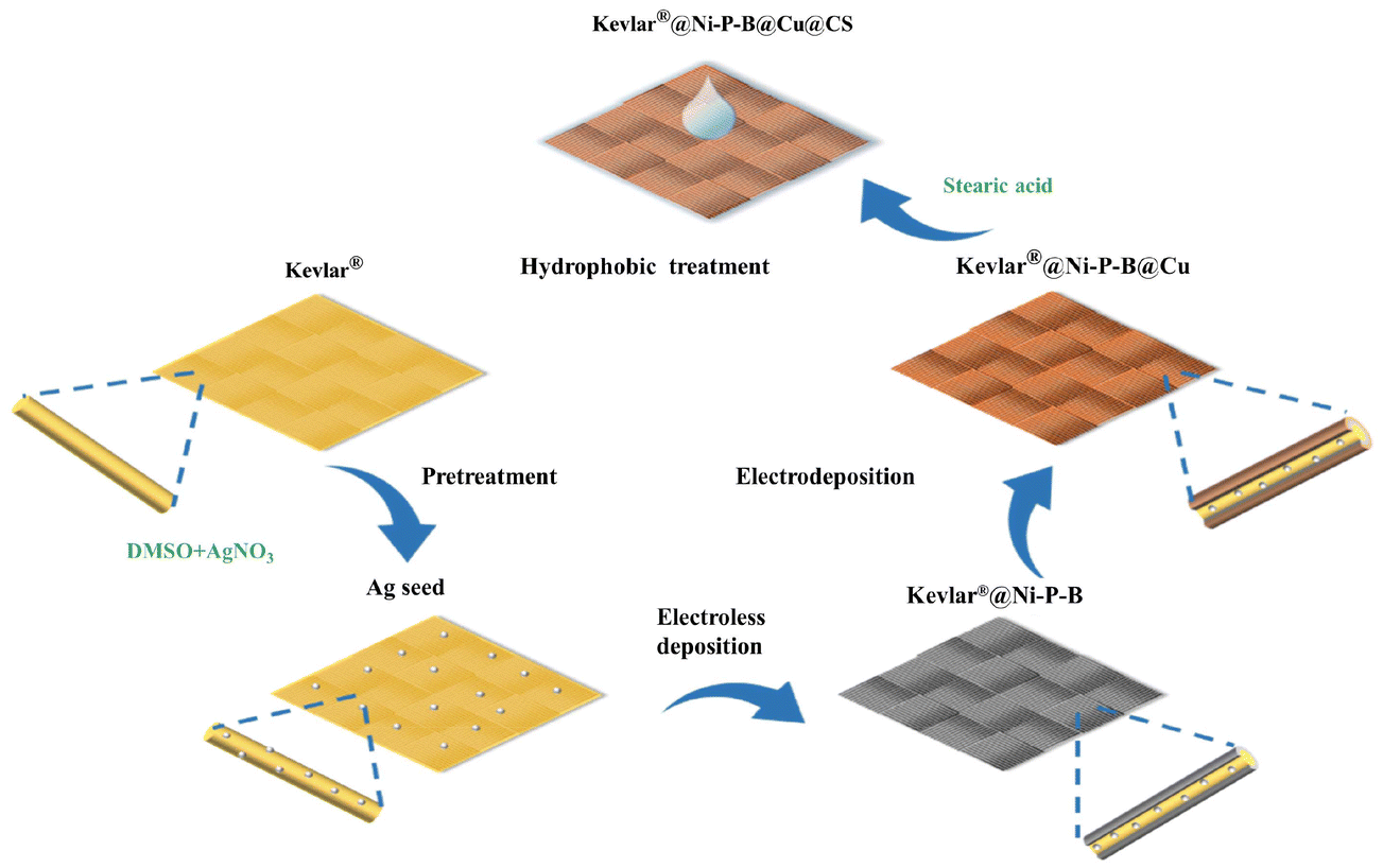 | ||
| Fig. 1 Schematic of the preparation route for the Kevlar®@Ni–P–B@Cu@CS composite fabric. | ||
| Composition | Role | Concentration and condition |
|---|---|---|
| Cu2(OH)2CO3 | Copper salt | 45–55 g L−1 |
| C6H10O8·H2O | Complexant | 200–250 g L−1 |
| NaKC4H4O6·4H2O | 20–40 g L−1 | |
| NaHCO3 | Conducting salt | 20–25 g L−1 |
| KOH | pH adjuster | 180–230 g L−1 |
| TEA | 2–3 mL L−1 | |
| NH3·H2O | 2–3 mL L−1 | |
| SeO2 | Additive | 0.01–0.02 g L−1 |
| pH | 9–9.5 | |
| T | 45–55 °C |
2.3 Characterization
The surface morphologies of the coated Kevlar® fabric were investigated using scanning electron microscopy (SEM, Nova NanoSEM 450, FEI). Elemental mapping was performed using an energy-dispersive spectroscopy system (EDS, X-act, Oxford) equipped with SEM. The surface chemical compositions of the samples were examined using an X-ray photoelectron spectroscopy instrument (XPS, ESCALAB 250Xi, Thermo Scientific) with an Al Kα X-ray source (1486.6 eV). The crystal structures of the Ni–P–B layer and Cu layer on the Kevlar® fabric were characterized by X-ray diffractometry (XRD) on a D8 Advance instrument (Bruker). The contact angle (CA) was measured three times at different positions with a water volume using a contact angle meter (OCA20, Dataphysics) and then averaged. The areal weight gain of the coating was calculated using the following equation:| W = (m1 − m0)/S, | (1) |
The surface electrical resistance of the sample was measured using a four-probe meter (RTS-8, 4-Probs Tech Ltd). An electrochemical analyzer (CHI760E, Chenhua) was used to conduct potentiodynamic polarization measurements to assess the corrosion resistance of the samples. Specifically, the test was conducted in 3.5 wt% NaCl solution under ambient conditions after a stable open circuit was potentially established using a classic three-electrode system with platinum as the counter electrode, saturated calomel electrode as the reference electrode, and the sample as the working electrode.
A vector network analyzer (Agilent E5071C) was used to measure the EMI-shielding efficiency (EMI-SE) using the waveguide method according to ASTM D5568-14 standard. The scattering parameters (S11 and S21) of the fabrics (22.9 × 10.2 mm) in the frequency range of 8.2–12.4 GHz (X-band) were investigated using the vector network analyzer to calculate the reflection coefficient (R), transmission coefficient (T), and absorption coefficient (A). The total EMI-SE (SET), microwave reflection (SER), and microwave absorption (SEA) of the samples were calculated using the following equations:
| R = |S11|2 | (2) |
| T = |S12|2 | (3) |
| A = 1 − R − T | (4) |
 | (5) |
 | (6) |
 | (7) |
The sample was wrapped around a cylindrical glass rod with a diameter of 10 mm for the bending test. The tape-peeling test was conducted by initially attaching a tape to the fabric surface, then rolling a balance weight of 200 g twice on the tape to make it evenly adhere to the surface of the fabric, and finally pulling it off quickly. A four-probe resistance meter was used to measure the resistance values every 100 times (for the bending test) and every 50 times (for the tape-peeling test). Finally, the CA of the sample was tested after 500 times of bending test and 300 times of the tape test, respectively. The samples were placed in an extreme environment (T = 80 °C, RH = 98%) for 12 h to conduct the accelerated environmental test. The resistance was measured every 2 h, and the CA was tested after 12 h.
3. Results and discussion
As shown in Fig. S2a,† the original Kevlar® fabric exhibited a smooth surface without significant protrusions or grooves. After pretreatment of the sample, a large number of silver nanoparticles were successfully anchored on the substrate surface (Fig. S2b and S2c†), which served as the nucleation centers and riveting points for the subsequent electroless plating. Different plating times were chosen to investigate the formation process of the base coating (Fig. S3†). When the deposition time was 120 min (Fig. S3d†), the metallic particles began to interconnect within the thin film firmly bonded on the fabric substrate, forming a complete and continuous conductive metal network with a smooth and dense surface. When the plating time continued to be extended, local aggregation of the metallic particles occurred and formed a rough surface, which was detrimental to the successive electrodeposition. Therefore, the optimal time for the electroless plating was 120 min; at this time, the areal weight gain of the coating was approximately 69.12 g m−2 with a sheet electrical resistance of 542.3 mΩ sq−1. Moreover, XPS analysis confirmed the coating was composed of Ni, P, and B elements (Fig. S4†), while the XRD pattern confirmed its amorphous structure (Fig. S5†). The obtained sample was denoted as Kevlar®@120-Ni–P–B in this study and used as the substrate for the subsequent Cu electroplating.3.1 Selection of the optimal plating current density
Fig. 2a–2e show the SEM images demonstrating the surface morphologies of the Cu coatings formed after electroplating for 30 min at different electrical current densities. It could be seen that Cu particles were clustered on the surface of the Kevlar®@120-Ni–P–B fabric at a current density (I) of 20 mA cm−2 (Fig. 2a). The coating continued with smaller Cu grains at the current density of I = 25 mA cm−2, but the surface remained rough (Fig. 2b). When the current density increased to I = 30 mA cm−2, the deposited Cu nanoparticles were refined, resulting in a smooth and compact coating (Fig. 2c). As the current density increased further (I = 35 mA cm−2), the surface of the Cu coating gradually became undulating. Pinholes and nodules began to appear on the coating surface at the current density of I = 40 mA cm−2 (Fig. 2e). The coating nucleation rate was low at a low current density, thus making the particles aggregated and locally grown. Both the metal ion-transport rate and the coating nucleation rate were enhanced at higher current densities, resulting in a uniform distribution of the coating grains. However, when the current density became extremely large, the rapid deposition rate and the intensification of hydrogen evolution would lead to local singeing and nodulation of the coating surface. From the above discussion, a relatively flat surface morphology could be obtained at current densities of I = 25, 30, and 35 mA cm−2. The areal weight gain and the sheet electrical resistance of the obtained coating at different current densities are shown in Fig. S6.† The areal weight gain continued to increase with the increase in current density (also accompanied by an increase in stiffness), whereas the electrical resistance gradually decreased as the current density exceeded 30 mA cm−2.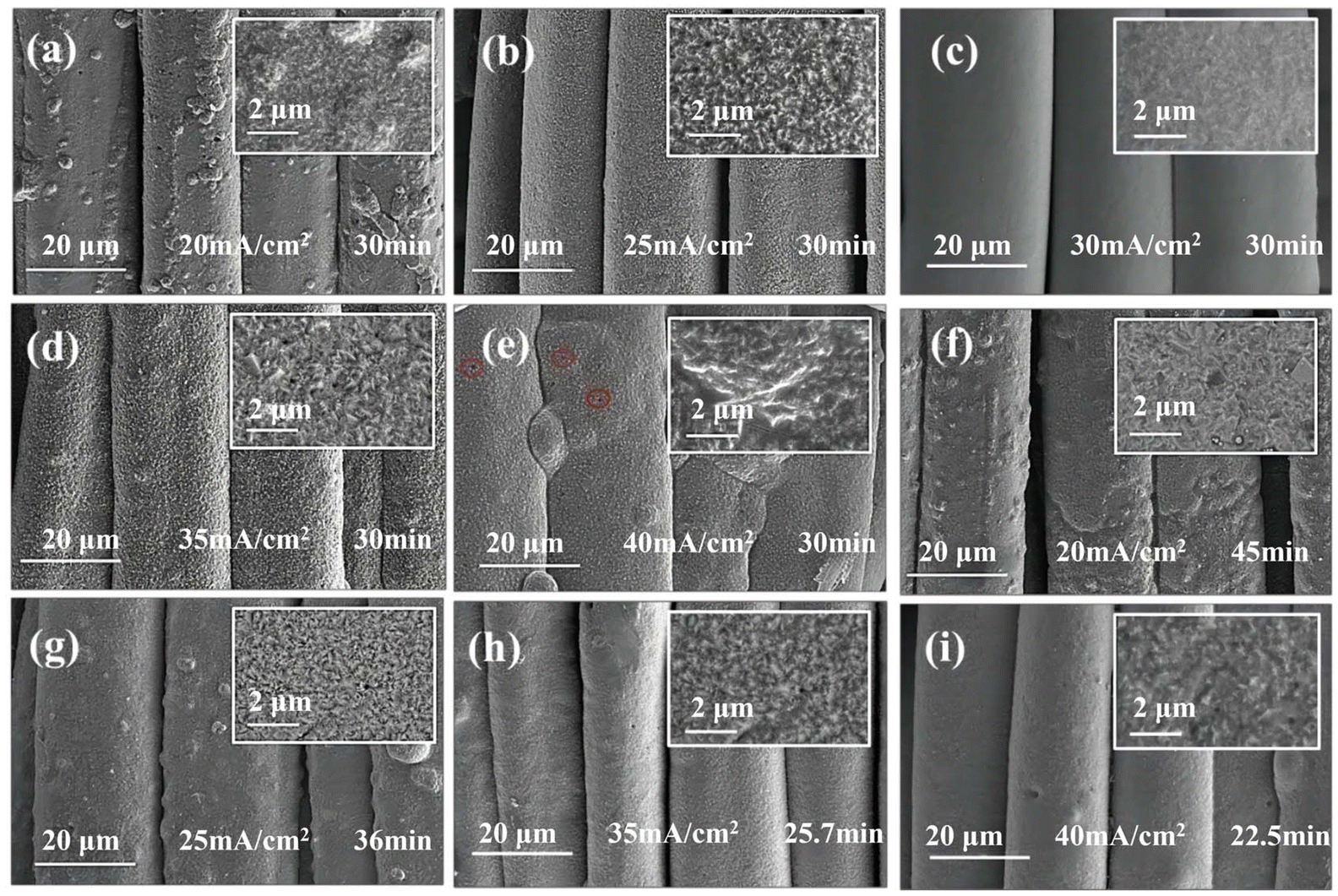 | ||
| Fig. 2 Surface morphology of the Kevlar®@Ni–P–B@Cu fabrics: (a–e) at different current densities; (f–i) at the same weight gain. | ||
By varying the plating current and time, different Cu coatings with the same weight gain (a moderate value of 188.11 g m−2) were prepared to further investigate the influence of the current density. The specific approach was to extend the coating time at low current density and reduce the coating time at high current density. The surface of the Kevlar®@Ni–P–B@Cu fabric remained rough at a low current density. The Cu nanoparticles continued to aggregate even with compensation from the time extension (Fig. 2f and g). At higher current density, a smoother surface was achieved by reducing the plating time (Fig. 2h and 2i). Although the deposition efficiency was improved, defects, such as pinholes and nodulations, appeared at the early stage of deposition. Therefore, it can be inferred from the comparison between Fig. 2(c) and (f–i) that the optimal current density was I = 30 mA cm−2.
3.2 Effect of time on Cu electrodeposition
After the optimal current density (I = 30 mA cm−2) was determined, the evolution of the deposition morphology was studied by adjusting the electroplating time (T) to prepare Kevlar®@Ni–P–B@Cu fabrics with different morphologies and properties. As shown in Fig. 3a–c, a limited number of spherical Cu nanoparticles (CuNPs) were uniformly dispersed and anchored on the surface of the Kevlar®@Ni–P–B fabric substrate, and the Ni–P–B base coating layer was visible within the first 5 min of electroplating. As the plating time increased, the deposition of the spherical CuNPs continued to grow and gradually covered the whole substrate with the extension of the plating time (Fig. 3d and e). A preliminary conductive Cu network was formed as all the CuNPs linked together (Fig. 3f). However, the metal luster on the surface was weak at this time due to the insufficient thickness (Fig. 3i). When the plating time was 30 min, the Kevlar®@Ni–P–B@Cu fabric exhibited a dense, smooth, and flat surface coating without aggregates or gullies (Fig. 3g), considerably improving the metal luster. The Kevlar®@Ni–P–B@Cu composite fabric retained its great inherent flexibility and lightweight characteristics (Fig. 3i), allowing for easy bending and curling, making it suitable for flexible device applications. As time progressed, the surface of the coating gradually became rough (Fig. 3h) again, and the softness of the composite fabric decreased as the thickness of the Cu layer increased.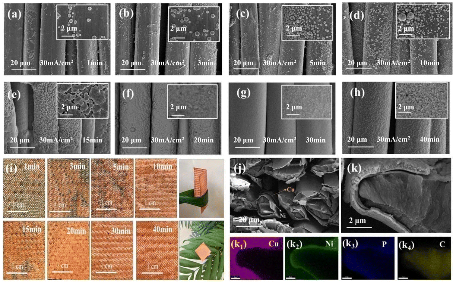 | ||
| Fig. 3 (a–h) SEM images of the Kevlar®@Ni–P–B@Cu fabric surfaces, and (i) the corresponding digital photos; (j–k) SEM images of the cross-sectional morphology; (k1–k4) EDS mapping images. | ||
Successful preparation of the Kevlar®@Ni–P–B@Cu fabric with a double-coating structure was confirmed using the SEM imaging of the cross-sectioned plated fabric (at a plating time of 30 min) (Fig. 3j–k). The results show that the thickness of the Ni–P–B layer on the Kevlar® was approximately 200–300 nm, while the Cu layer on the Ni–P–B layer was approximately 400–600 nm. The thinness of both coatings could preserve the softness of the fabric to a significant degree. Furthermore, both loaded layers presented a fascinating cross-sectional morphology, implying the high density and uniformity of each coating and the controllable deposition. Fig. 3k1–4 depicts the element distribution of the inner Ni–P–B coating and the outer Cu coating. Because EDS has low resolution, it could not automatically detect and identify the presence of the boron element.
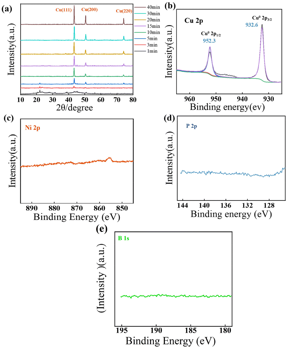
Fig. 4a shows the XRD patterns of the Kevlar®@Ni–P–B@Cu composite fabrics prepared with different plating times. Broad diffraction peaks appeared at 2θ = 20.0°–30.0°, which were the characteristic peaks of the poly(p-phenylene terephthalamide) polymer crystal structure of Kevlar®. The peaks at 2θ = 43.3°, 50.4°, and 74.1° were assigned to the (111), (200), and (220) lattice planes of the face-centered cubic Cu crystalline structure, which were completely in accordance with the standard PDF card #04-0836. The peak intensity of the (111), (200), and (220) crystal planes considerably increased with the increasing plating time, while the diffraction peaks of the Kevlar® substrate declined and disappeared. This phenomenon was attributed to the continuously increasing Cu load and the improvement of the crystal structure. Furthermore, no signals of oxide impurities (such as CuO and Cu2O) were observed from the XRD results. In addition, as the deposition of Cu increased, the broad, amorphous peak of the underlying Ni–P–B coating was almost invisible.
 | ||
| Fig. 4 (a) XRD patterns of the Kevlar®@Ni–P–B@Cu fabrics at different electroplating times; high-resolution XPS spectra of (b) Cu 2p,59 (c) Ni 2p, (d) P 2p, and (e) B 1s for Kevlar®@Ni–P–B@Cu at the electroplating time of 30 min. | ||
To validate the chemical state of the Cu coating, XPS characterization was conducted on the Kevlar®@Ni–P–B@Cu composite fabric at an electroplating time of 30 min, and the results are shown in Fig. 4b–d. The Cu 2p peaks consisted of a small peak at 932.6 eV assigned to Cu0 2p3/2, and a large peak at 952.6 eV assigned to Cu0 2p1/2. No other peaks were observed except for these two splitting peaks, indicating that the surface composition of the composite contained only metallic Cu0 with no oxidation components. As the Cu coating completely covered the underlying Ni–P–B layer, the constituent elements of the latter could not be detected by XPS.
We then investigated the trends for the areal weight gain, sheet electrical resistance, and EMI-shielding performance over the electroplating time. The results are summarized in Fig. 5. The areal weight gain of the Cu coating continuously increased from 6.00 to 265.33 g m−2 with increasing the electroplating time from 1 to 40 min (Fig. 5a). As the weight gain grew further with the extension of plating time, it resulted in a decrease in toughness. Moreover, the sheet electrical resistance of the Kevlar®@Ni–P–B@Cu fabric rapidly decreased from 427.5 to 12.6 mΩ sq−1 with the increasing plating time from 1 to 15 min. However, the reduction in electrical resistance became gradual when the plating time varied from 15 to 40 min, especially from 30 to 40 min (Fig. 5a), when a complete, continuous, and dense coverage of CuNPs facilitated the formation of a highly conductive network (Fig. 4). The high conductivity directly contributed to a high EMI-SE. Hence, the conductivity level has a certain reference value, which is a critical factor in determining the effectiveness in providing EMI shielding.
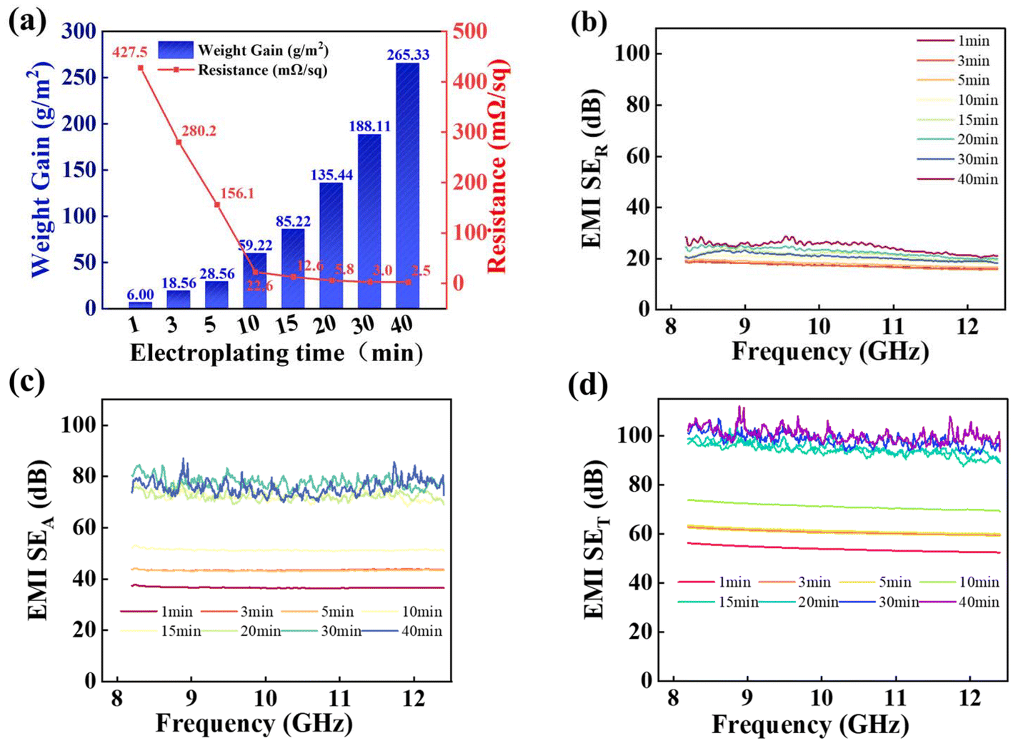 | ||
| Fig. 5 (a) Areal weight gain and sheet resistance of the Kevlar®@Ni–P–B@Cu fabrics at different plating times; (b–d) EMI SER, SEA, and SET curves of the Kevlar®@Ni–P–B@Cu fabrics at different plating times in the X-band. | ||
A systematic measurement of the EMI-SE value for the Cu-decorated Kevlar® fabric at various electroplating times was conducted in the wave-frequency range of 8.2–12.4 GHz, and the results were consistent with the variation trend of the conductivity. The average SET value of the Kevlar®@Ni–P–B@Cu fabric increased from 53.9 dB to 100.3 dB as the plating time increased from 1 min to 40 min, but the increase was actually small after plating for more than 15 min (Fig. 5d). Fig. 5b and c show the SE values of the reflection (SER) and the adsorption (SEA) parts, respectively. The results showed that the increase in plating time improved both the SET and SEA values but had a minimal effect on the SER. The obtained values confirmed that the shielding was absorption-dominated, and the absorbed EM waves were significantly more than those blocked by reflection, thus reducing the environmental pollution from the secondary radiation.
The Cu-loading capacity on the Kevlar®@Ni–P–B fabric was adjusted by varying the electroplating time, which made the morphology, structure, areal weight gain, electrical conductivity, and EMI-shielding performance of the composite fabric be regulated. However, from the above-mentioned discussion, the optimal balance between conductivity and toughness was achieved at the plating time of 30 min; thus, 30 min was considered as the optimal choice.
The major EMI-shielding mechanisms in the Kevlar®@Ni–P–B@Cu system are demonstrated in Fig. 6. When EM waves reach the surface of the composite fabric from the atmosphere, the outer surface of Cu coating provides numerous scattering points due to the impedance mismatch, thereby restricting the entry of some EM waves through reflection attenuation. The remaining EM waves enter the internal Kevlar®@Ni–P–B@Cu fabric, and are subsequently attenuated through multiple internal reflections between the fibers in the woven superstructure and the absorption from the superior conductive network constructed by the Cu and Ni–P–B bicoatings. (Fig. 6a). More specifically, for a single Kevlar®@Ni–P–B@Cu fiber, EM waves experience multi-reflections within the adjacent fiber arrays, and then are attenuated by the highly effective conductive loss/multiple interface reflection inside the multilayers of the Kevlar®@Ni–P–B@Cu fiber (Fig. 6b). The synergistic effect of the superior conductive networks, specific Kevlar® woven superstructure, and multilayered microstructure can thus greatly enhance the dissipation of EM waves, which will eventually become invisible on the other side of the composite fabric. It is especially noteworthy that the multiple internal reflections will extend the transmission path of EM waves inside the fabric, and will produce a large amount of additional multichannel absorption.
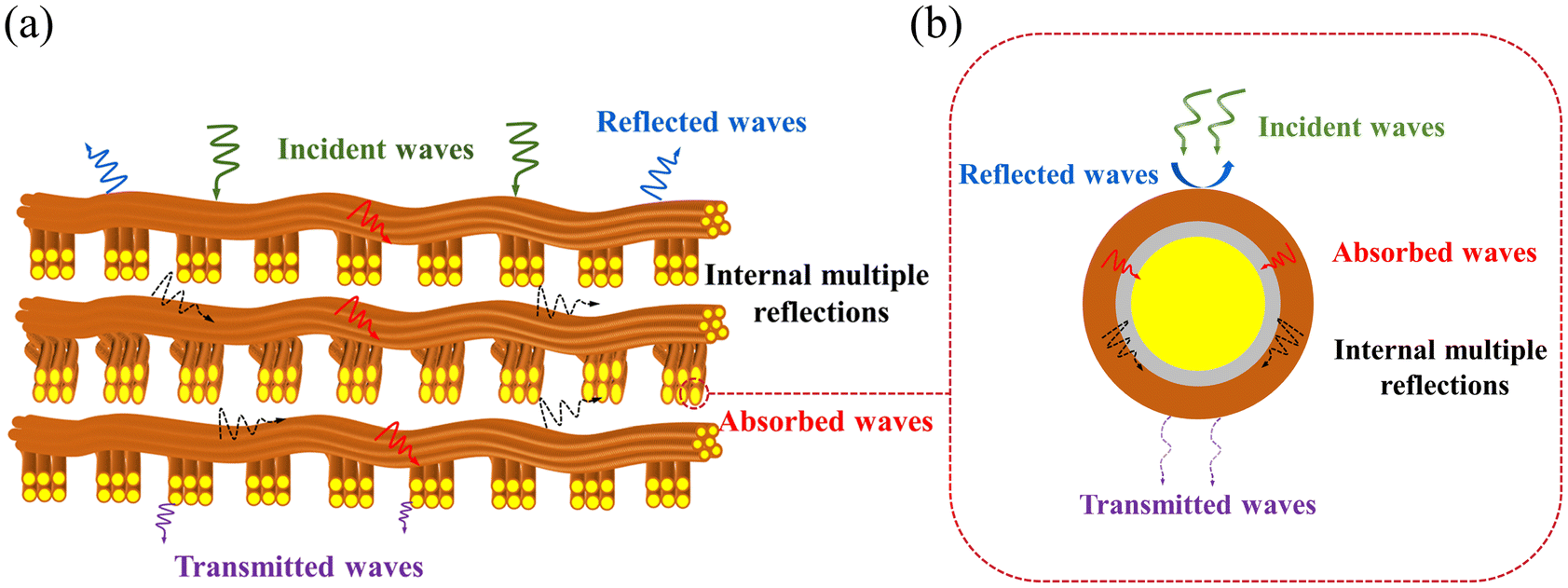 | ||
| Fig. 6 EMI-shielding mechanisms of the Kevlar®@Ni–P–B@Cu system: (a) shielding mechanisms of the Kevlar®@Ni–P–B@Cu fabric, (b) shielding mechanisms of a single Kevlar®@Ni–P–B@Cu fiber. | ||
3.3 Influence of SA modification on Kevlar®@Ni–P–B@Cu
EMI-shielding materials are often exposed to external pollution, and when they are contaminated, their appearance and functionality can be significantly reduced. The development of new multifunctional EMI-shielding materials with superhydrophobicity is crucial for wearable electronic devices to ensure the long-term durability of the whole system. Thus, the optimized Kevlar®@Ni–P–B@Cu fabric was immersed into a stearic acid/anhydrous ethanol solution for modification and testing.Fig. 7a shows the structural formula after the combination of SA and copper, and Fig. 7b shows the Fourier transform infrared (FTIR) spectrum of the coating surface. The absorption peaks located at 2916 and 2847 cm−1 corresponded to the asymmetric and symmetric stretching vibrations of the methyl functional group (–CH2–), respectively. Two absorption peaks appeared at 1584 and 1442 cm−1, which could be assigned to the asymmetric stretching of the carboxyl (–COO) group and the C–H bending of CS, respectively.60 The characteristic absorption peak of the long carbon chain methylene was at 718 cm−1, indicating the existence of long-chain fatty groups. The results above confirmed the successful self-assembly of the CS monolayer on the outermost surface of the Cu coating after the SA modification.
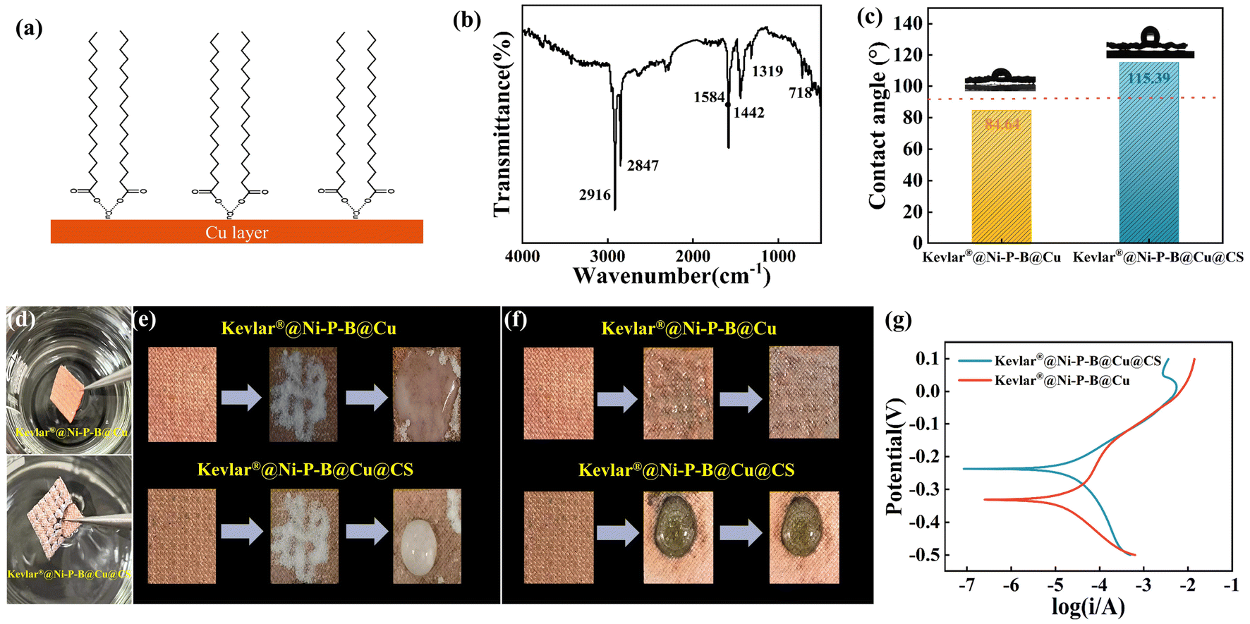 | ||
| Fig. 7 (a) Structure diagram of the self-assembled monolayer; (b) FTIR spectrum of the Kevlar®@Ni–P–B@Cu@CS fabric; (c) CAs of the Kevlar®@Ni–P–B@Cu and the Kevlar®@Ni–P–B@Cu@CS fabric; digital photos demonstrating (d) the water repellency, (e) the self-cleaning ability, and (f) the self-protection ability before and after SA modification; (g) potentiodynamic polarization curves in 3.5%NaCl solution. | ||
Fig. 7c illustrates the CA of the composite fabric before and after SA treatment. The static CAs of the Kevlar®@Ni–P–B@Cu and the Kevlar®@Ni–P–B@Cu@CS fabric with a dimension of 20 × 10 mm to water were recorded as 84.64° and 115.39°, respectively, indicating the significant increase in hydrophobicity. As shown in Fig. 7d, the Kevlar®@Ni–P–B@Cu fabric was completely hydrophilic and wetted easily by water. However, after SA modification, the surface with a low surface energy structure conformed to the typical Cassie-Baxter state,11 which could capture surrounding air pockets and prevent liquid droplets from penetrating.28,61 The sample modified with SA initially contained a certain amount of air on its surface microstructure, which was then fixed between water and the sample after it was placed in an aqueous solution. As a result, the modified sample exhibited a typical underwater “silver mirror” phenomenon due to the complete reflection of light when transmitted from the water to the air interface with an incident angle greater than the critical angle.11
Moreover, high hydrophobicity also endowed the modified fabric with a good self-cleaning property. The sample was tilted at a certain angle and covered with a certain amount of pollutants (simulating dust and stains using NaHCO3 powders), as shown in Fig. 7e. The water droplet immediately mixed with the pollutants and completely spread over the sample surface when it was placed on the Kevlar®@Ni–P–B@Cu fabric, while the pollutants dissolved in the water droplet and slid down along the movement direction for the Kevlar®@Ni–P–B@Cu@CS fabric, thus presenting an outstanding self-cleaning ability.
The Kevlar®@Ni–P–B@Cu@CS fabric could also protect itself when contacting corrosive droplets, such as ammonium sulfide (Fig. 7f). This was used to simulate a sulfide atmosphere, which is an important factor causing the corrosion and discoloration of metallic copper in air. Here, the droplet completely infiltrated into the Kevlar®@Ni–P–B@Cu fabric, which was thus significantly deteriorated and discolored after 5 min of dripping. However, only a small portion of the Kevlar®@Ni–P–B@Cu@CS fabric contacted by the droplet was discolored.
The corrosion property of the composite fabric before and after SA treatment was also examined by testing the potentiodynamic polarization curve in 3.5 wt% NaCl solution representing a sweaty environment. The corrosion current density (icorr) and corrosion potential (Ecorr) were calculated by intersecting the cathodic and anodic polarization curves. The icorr of the two fabrics were 2.28 × 10⁻⁵ and 2.15 × 10⁻⁵ A cm−2, respectively. The corrosion potential of the Kevlar®@Ni–P–B@Cu@CS fabric increased to −0.22 from the −0.36 V of the Kevlar®@Ni–P–B@Cu fabric, indicating that the corrosion resistance of the composites was significantly improved after SA modification.
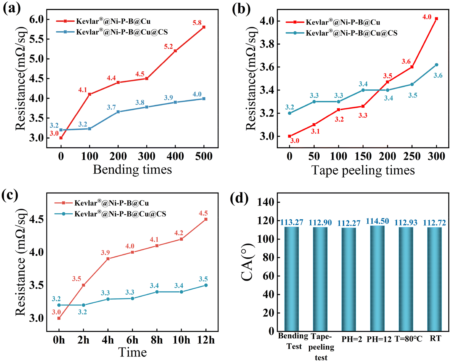
Considering the frequent application of the composite fabric in scenarios involving movement, friction, high temperature, high humidity, high acidity, and strong alkalinity, it is crucial to maintain the conductivity and hydrophobicity of the composite fabric under the circumstances mentioned above. In this study, the environmental durabilities of both the Kevlar®@Ni–P–B@Cu and Kevlar®@Ni–P–B@Cu@CS fabrics were fully evaluated through the bending test, taping test, high temperature and humidity environment test, and immersion in aqueous solutions of pH = 1 and pH = 12 for 12 h, respectively.
For the cyclic bending test, the fabric was wrapped around a cylindrical glass rod with a small radius of 5 mm. The smaller the curvature radius, the greater the damage to the shielding material. Fig. 8a illustrates the changes in the sheet resistance of the composite material within 500 bending cycles. The resistance of the Kevlar®@Ni–P–B@Cu fabric increased from the pristine 3.0 to 5.8 mΩ sq−1 after 500 bending cycles, while the resistance of the Kevlar®@Ni–P–B@Cu@CS fabric slightly increased from the pristine 3.2 to 4.0 mΩ sq−1. In addition, the CA of the Kevlar®@Ni–P–B@Cu@CS decreased by 2.12° after 500 bending cycles (Fig. 8d), still retaining 98.2% of its high hydrophobicity before bending.
 | ||
| Fig. 8 Resistances of the Kevlar®@Ni–P–B@Cu and the Kevlar®@Ni–P–B@Cu@CS fabric: (a) after the bending test, (b) after the tape-peeling test, and (c) after exposure to an accelerated environment test (T = 80 °C, RH = 95% for 12 h); (d) CAs of the Kevlar®@Ni–P–B@Cu@CS fabric after the different tests. | ||
After 300 times of tape-peeling tests, the sheet resistance of the Kevlar®@Ni–P–B@Cu fabric increased from 3.0 to 4.0 mΩ sq−1, while the resistance of the Kevlar®@Ni–P–B@Cu@CS fabric increased with a smaller change from 3.2 to 3.6 mΩ sq−1 (Fig. 8b). Moreover, the CA of the Kevlar®@Ni–P–B@Cu@CS fabric slightly decreased from 115.39° to 112.90° after tape-peeling for 300 times (Fig. 8d), maintaining 97.8% of the high hydrophobicity before tape-peeling. The presence of CS significantly enhanced the interfacial capability of the composite material, thus reducing the negative impact of the external forces (such as friction and bending) in service.
The CAs of the Kevlar®@Ni–P–B@Cu@CS remained at 112.27° and 114.50° after it was immersed in acid (pH = 2) and alkali (pH = 12) solutions for 12 h, respectively (Fig. 8d). The corresponding sheet resistances of the Kevlar®@Ni–P–B@Cu and Kevlar®@Ni–P–B@Cu@CS were tested to be 4.2 and 3.6 mΩ sq−1 and 3.6 and 3.5 mΩ sq−1 in acid and alkali solutions, respectively. Both results show the improvement of the corrosion resistance in acid and alkali solutions after the SA modification.
Both the Kevlar®@Ni–P–B@Cu and Kevlar®@Ni–P–B@Cu@CS fabrics were exposed to high-temperature (T = 80 °C) and high-humidity (RH = 95%) environments for 12 h, with a cycle of every 2 h, and the resistance curves are presented in Fig. 8c. The sheet resistance of the Kevlar®@Ni–P–B@Cu fabric increased from 3.0 to 4.7 mΩ sq−1, whereas that of the Kevlar®@Ni–P–B@Cu@CS fabric increased from 3.0 to 3.8 mΩ sq−1. Moreover, the CA of the Kevlar®@Ni–P–B@Cu@CS fabric was 112.93°, retaining 97.9% of its pristine hydrophobicity. Furthermore, the CA and the sheet resistance of the Kevlar®@Ni–P–B@Cu@CS fabric were 112.72° and 3.5 mΩ sq−1, respectively, after 60 d of exposure to air at room temperature (RT), showing a slight performance degradation.
All these findings demonstrate the high durability of the SA-modified Kevlar®@Ni–P–B@Cu@CS fabric, which could substantially preserve its excellent properties in harsh environments.
Just as the electrical conductivity slightly decreased with the sheet resistance increasing from 3.0 to 3.2 mΩ sq−1, the EMI-shielding performance of the SA-modified Kevlar®@Ni–P–B@Cu@CS fabric also slightly decreased, with the average EMI-SE value decreasing from 98.4 to 93.9 dB in the X-band (Fig. 9). This marginal disadvantage was negligible compared with the significant improvements in hydrophobicity, corrosion resistance, and environmental stability. The enhanced liquid repellency, excellent self-cleaning property, better self-protection in corrosive environments, higher mechanical stability, and durability of the Kevlar®@Ni–P–B@Cu@CS fabric make it a promising and applicable wearable technology that can be used in harsh environments. In addition, the facile self-assembly treatment does not require additional sintering or heat treatment at high temperatures, such as conventional hydrophobic treatment. Its process is simple and easy to operate but brings significant protective effects without a noticeable reduction in conductivity or EMI-shielding performance, making it suitable for industrial production.
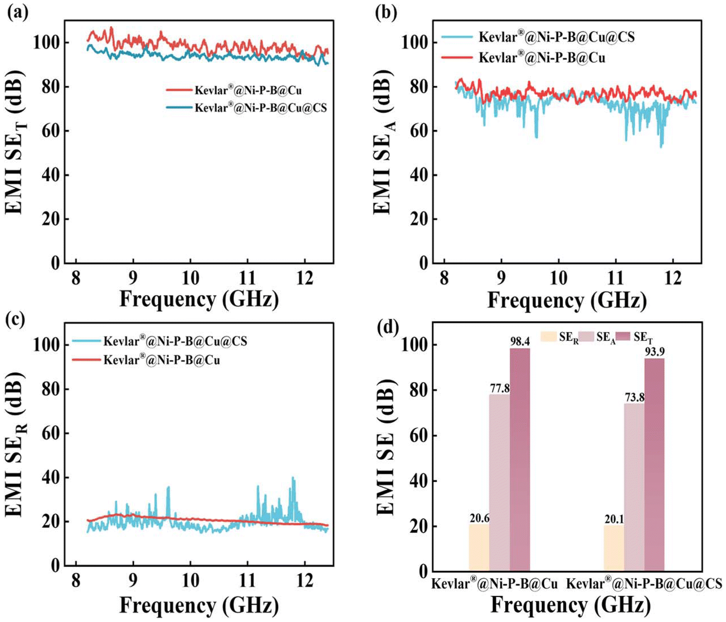 | ||
| Fig. 9 EMI-SET, SEA, and SER curves of the Kevlar®@Ni–P–B@Cu and the Kevlar®@Ni–P–B@Cu@CS fabric in the X-band. | ||
4. Conclusion
In this work, Kevlar® fabric was initially coated with an ultra-thin amorphous Ni–P–B layer using electroless plating. Then, a compact and smooth nanocrystalline Cu layer was subsequently coated on the fabric via electroplating. The optimal electroplating current and time were determined to be 30 mA cm−2 and 30 min, respectively. The thickness of the whole bilayer coating was less than 500 nm, which was 2.5% of the diameter of the substrate Kevlar® fiber. The optimized Kevlar®@Ni–P–B@Cu interconnected network provided an effective conductive path for electron transport and presented an extremely low electrical resistance (3.0 mΩ sq−1), which was beneficial to improving the conductive loss of the incident EM waves. Multiple internal reflections occurred and extended the transmission path of the EM waves inside the fabric, and produced a large amount of additional multichannel absorption. The synergistic effect of the superior conductive networks, specific Kevlar® woven superstructure, and multilayered microstructure greatly enhanced the dissipation and absorption of EM waves, and led to a superb EMI-shielding performance with an average SE of 98.4 dB in the X-band. Finally, the metallic Cu coating was innovatively modified through a facile SA self-assembly treatment with no sintering or heating curing process. The SA self-assembled monolayer acted as an effective outermost protective layer, and the obtained Kevlar®@Ni–P–B@Cu@CS composite fabric achieved a remarkable self-cleaning capability and good water repellency (with a CA of 115.39°, increased from 84.64° of the original Kevlar®@Ni–P–B@Cu), retained a low electrical resistivity (3.2 mΩ sq−1), and demonstrated an excellent EMI-shielding performance (with an average SE of 93.9 dB). The low electrical resistivity of the Kevlar®@Ni–P–B@Cu@CS composite fabric was better maintained after the accelerated durability test and corrosive environment treatment compared with that of Kevlar®@Ni–P–B@Cu, and the good water repellency of the SA monolayer withstood the relevant test.Author contributions
Qinsi Shao: conceptualization, methodology, software, writing – review & editing. Hao Wang: formal analysis, investigation, data curation, visualization, writing – original draft. Leilei Zhang: validation, investigation, writing – original draft. Xihai Wang: investigation, resources. Hengxin Zhang: investigation, resources. Ruicheng Bai: supervision, project administration. Hongshan Fu: funding acquisition.Conflicts of interest
The authors declare that they have no known competing financial interests or personal relationships that could have appeared to influence the work reported in this paper.Acknowledgements
This work received financial support from National Natural Science Foundation of China (No. 51803116).References
- A. Iqbal, F. Shahzad, K. Hantanasirisakul, M. K. Kim, J. Kwon, J. Hong, H. Kim, D. Kim, Y. Gogotsi and C. M. Koo, Science, 2020, 369, 446–450 CrossRef CAS PubMed
.
- B. Zhao, H. Wu, Q. Tian, Y. Li, F. Qiu and T. Zhang, ACS Appl. Mater. Interfaces, 2023, 15(6), 8751–8760 CrossRef CAS PubMed
- M. Zhu, X. Yan, Y. Lei, J. Guo, Y. Xu, H. Xu, L. Dai and L. Kong, ACS Appl. Mater. Interfaces, 2022, 14, 14520–14531 CrossRef CAS PubMed
- Y. M. Chen, Y. Yang, Y. Xiong, L. Zhang, W. H. Xu, G. G. Duan, C. T. Mei, S. H. Jiang, Z. H. Rui and K. Zhang, Nano Today, 2021, 38, 101204 CrossRef CAS
- F. Peng, W. Zhu, Y. Fang, B. Fu, H. Chen, H. Ji, X. Ma, C. Hang and M. Li, ACS Appl. Mater. Interfaces, 2023, 15, 4284–4293 CrossRef CAS PubMed
- D. D. L. Chung, Mater. Chem. Phys., 2020, 255, 123587 CrossRef CAS
- Z. Zhang, L. Cheng, P. Kroll, J. Tan and W. Yang, Appl. Surf. Sci., 2022, 590, 153151 CrossRef CAS
- X. Sun, J. H. Fu, C. Teng, M. Zhang, T. Liu, M. Guo, P. Qin, F. Zhan, Y. Ren, H. Zhao, L. Wang and J. Liu, ACS Appl. Mater. Interfaces, 2022, 14, 33650–33661 CrossRef CAS PubMed
- Y. Zhang, H. Wu and S. Guo, ACS Appl. Mater. Interfaces, 2022, 14, 40351–40360 CrossRef CAS PubMed
- T. Kim, S. Pak, J. Lim, J. S. Hwang, K. H. Park, B. S. Kim and S. Cha, ACS Appl. Mater. Interfaces, 2022, 14, 13499–13506 CrossRef CAS PubMed
- X. Mei, L. Lu, Y. Xie, Y. X. Yu, Y. Tang and K. S. Teh, ACS Appl. Mater. Interfaces, 2020, 12, 49030–49041 CrossRef CAS PubMed
- T. Pan, Y. Zhang, C. Wang, H. Gao, B. Wen and B. Yao, Compos. Sci. Technol., 2020, 188, 107991 CrossRef CAS
- B. Yao, W. Hong, T. Chen, Z. Han, X. Xu, R. Hu, J. Hao, C. Li, H. Li, S. E. Perini, M. T. Lanagan, S. Zhang, Q. Wang and H. Wang, Adv. Mater., 2020, 32, e1907499 CrossRef PubMed
- Y. Wang, W. Wang, X. Ding and D. Yu, Chem. Eng. J., 2020, 380, 122553 CrossRef CAS
- Y. An, C. Luo, D. Yao, S. Wen, P. Zheng, S. Chi, Y. Yang, J. Chang, Y. Deng and C. Wang, Nano-Micro Lett., 2021, 13, 84 CrossRef CAS PubMed
- B. Yao, W. Hong, T. W. Chen, Z. B. Han, X. W. Xu, R. C. Hu, J. Y. Hao, C. H. Li, H. Li, S. E. Perini, M. T. Lanagan, S. L. Zhang, Q. Wang and H. Wang, Adv. Mater., 2020, 32, 1907499 CrossRef CAS PubMed
- L. C. Jia, L. Xu, F. Ren, P. G. Ren, D. X. Yan and Z. M. Li, Carbon, 2019, 144, 101–108 CrossRef CAS
- Z. Xiang, C. Huang, Y. Song, B. Deng, X. Zhang, X. Zhu, D. Batalu, O. Tutunaru and W. Lu, Carbon, 2020, 167, 364–377 CrossRef CAS
- M. Dai, Y. Zhai and Y. Zhang, Chem. Eng. J., 2021, 421, 127749 CrossRef CAS
- W. Gu, J. Sheng, Q. Huang, G. Wang, J. Chen and G. Ji, Nano-Micro Lett., 2021, 13, 102 CrossRef CAS PubMed
- T. B. Yang, J. Y. Zong, H. Lin, D. X. Yan, J. Lei and Z. M. Li, Chem. Eng. J., 2023, 476, 146570 CrossRef CAS
- K. Wang, Q. Ma, Y. M. Zhang, S. D. Wang and G. T. Han, Polymers, 2020, 12, 783 CrossRef CAS PubMed
- Z. Guo, P. Ren, Z. Lu, K. Hui, J. Yang, Z. Zhang, Z. Chen, Y. Jin and F. Ren, ACS Appl. Mater. Interfaces, 2022, 14, 41468–41480 CrossRef CAS PubMed
- H. Guo, Y. Li, Y. Ji, Y. Chen, K. Liu, B. Shen, S. He, G. Duan, J. Han and S. Jiang, CompComm, 2021, 27, 100879 Search PubMed
- S. Zhu, C. Xing, F. Wu, X. Zuo, Y. Zhang, C. Yu, M. Chen, W. Li, Q. Li and L. Liu, Carbon, 2019, 145, 259–265 CrossRef CAS
- C. Lan, L. Zou, N. Wang, Y. Qiu and Y. Ma, J. Colloid Interface Sci., 2021, 590, 467–475 CrossRef CAS PubMed
- X. Mei, L. Lu, Y. Xie, Y.-X. Yu, Y. Tang and K. S. Teh, ACS Appl. Mater. Interfaces, 2020, 12, 49030–49041 CrossRef CAS PubMed
- S. Wang, D. Li, Y. Zhou and L. Jiang, ACS Nano, 2020, 14, 8634–8645 CrossRef CAS PubMed
- J. Yao, L. Zhang, F. Yang, Z. Jiao, X. Tao, Z. Yao, Y. Zheng and J. Zhou, Chem. Eng. J., 2022, 446, 136945 CrossRef CAS
- S. Uzun, M. Han, C. J. Strobel, K. Hantanasirisakul, A. Goad, G. Dion and Y. Gogotsi, Carbon, 2021, 174, 382–389 CrossRef CAS
- J. Liu, H. B. Zhang, R. Sun, Y. Liu, Z. Liu, A. Zhou and Z. Z. Yu, Adv. Mater., 2017, 29, 1702367 CrossRef PubMed
- P. Kumar, U. N. Maiti, A. Sikdar, T. K. Das, A. Kumar and V. Sudarsan, Polym. Rev., 2019, 59, 687–738 CrossRef CAS
- J. B. Tang, X. Zhang, J. Wang, R. Q. Zou and L. J. Wang, Appl. Surf. Sci., 2021, 565, 150577 CrossRef CAS
- B. K. Little, Y. F. Li, V. Cammarata, R. Broughton and G. Mills, ACS Appl. Mater. Interfaces, 2011, 3, 1965–1973 CrossRef CAS PubMed
- Q. S. Shao, R. C. Bai, Z. Y. Tang, H. W. Pang, W. Yan, J. L. Sun and M. S. Ren, Ind. Eng. Chem. Res., 2015, 54, 11302–11311 CrossRef CAS
- Y. F. Zhou, W. Y. Li, L. L. Li, Z. H. Sun, L. Jiang, J. W. Ma, S. J. Chen, X. Ning and F. L. Zhou, J. Mater. Sci., 2021, 56, 6499–6513 CrossRef CAS
- Y. F. Zhou, Z. H. Sun, L. Jiang, S. J. Chen, J. W. Ma and F. L. Zhou, Appl. Surf. Sci., 2020, 533, 147431 CrossRef CAS
- Z. H. Sun, Y. F. Zhou, W. Y. Li, S. J. Chen, S. H. You and J. W. Ma, Coatings, 2019, 9, 599 CrossRef CAS
- H. R. Zhang, X. G. Zou, J. J. Liang, X. Ma, Z. Y. Tang and J. L. Sun, J. Appl. Polym. Sci., 2012, 124, 3363–3371 CrossRef CAS
- D. Chen, C. Liu and Z. Kang, Colloid Interface Sci. Commun., 2021, 40, 100365 CrossRef CAS
- D. R. Wang, Y. K. Zhang, X. Lu, Z. J. Ma, C. Xie and Z. J. Zheng, Chem. Soc. Rev., 2018, 47, 4611–4641 RSC
- W. X. Li, F. Guo, X. Q. Wei, Y. E. Du and Y. Q. Chen, RSC Adv., 2020, 10, 36644–36653 RSC
- X. Zhang, D. G. Miao, X. Ning, M. Cai, Y. H. Tian, H. M. Zhao and S. X. Jiang, Vacuum, 2019, 164, 205–211 CrossRef CAS
- M. S. Saleem, M. B. Hanif, M. Gregor, M. Motola and A. F. Khan, Appl. Surf. Sci., 2022, 596, 153584 CrossRef
- J. Lee, Y. Liu, Y. Liu, S.-J. Park, M. Park and H. Y. Kim, J. Mater. Chem. C, 2017, 5, 7853–7861 RSC
- S. Yang, Z. Kang and T. Guo, Nanotechnology, 2020, 31, 195710 CrossRef CAS PubMed
- H. Sun, L. Guo, N. Deng, X. Li, J. Li, G. He and J. Li, J. Alloys Compd., 2019, 810, 151907 CrossRef CAS
- Q. S. Shao, R. C. Bai, Z. Y. Tang, Y. F. Gao, J. L. Sun and M. S. Ren, Surf. Coat. Technol., 2016, 302, 185–194 CrossRef CAS
- H. Pang, R. Bai, Q. Shao, Y. Gao, A. Li and Z. Tang, Appl. Surf. Sci., 2015, 359, 280–287 CrossRef CAS
- X. D. Ding, W. Wang, Y. Wang, R. Xu and D. Yu, J. Alloys Compd., 2019, 777, 1265–1273 CrossRef CAS
- Y. Wang, W. Wang, X. D. Ding and D. Yu, Chem. Eng. J., 2020, 380, 122553 CrossRef CAS
- J. Li, G. Zhou, X. Jin, Y. Hong, W. He, S. Wang, Y. Chen, W. Yang and X. Su, Composites, Part B, 2018, 154, 257–262 CrossRef CAS
- F. Li, X. Xu, C. Cao, Z. Yang, G. Wang, T. Li, Y. Pu, S. Zhang, Z. Cheng, G. Lv, C. Xu, J. Xian, Y. Yang and Z. Pu, J. Cleaner Prod., 2023, 397, 136608 CrossRef CAS
- K. Bogomolov, E. Grishina and Y. Ein-Eli, J. Mater. Chem. A, 2023, 11, 24099–24113 RSC
- H.-x. Zhang, Q. Ma, Y.-z. Wang, B.-s. Xu and J.-j. Guo, Carbon, 2019, 150, 550–551 Search PubMed
- Y. Wu, W. Zhao, X. Zhu and Q. Xue, Carbon, 2019, 153, 95–99 CrossRef CAS
- N. Mishra, H. Madhad and D. Vasava, J. Heterocycl. Chem., 2021, 58, 1887–1913 CrossRef CAS
- J. Song, C. Chen, X. Du, X. Sun, P. Zhang, Y. Ma, H. Kong and M. Yu, Polym. Compos., 2023, 44, 2557–2568 CrossRef CAS
- P. Liu and J. M. Hensen, J. Am. Chem. Soc., 2013, 135, 14032–14035 CrossRef CAS PubMed
- M. Gönen, T. O. Egbuchunam, D. Balköse, F. İnal and S. Ülkü, J. Vinyl Addit. Technol., 2015, 21, 235–244 CrossRef
- H. Park, S. F. Ahmadi and J. B. Boreyko, Phys. Rev. Lett., 2021, 127, 044501 CrossRef CAS PubMed
Footnote |
| † Electronic supplementary information (ESI) available. See DOI: https://doi.org/10.1039/d3dt04291j |
| This journal is © The Royal Society of Chemistry 2024 |