
 Open Access Article
 This Open Access Article is licensed under a Creative Commons Attribution-Non Commercial 3.0 Unported Licence
A study of bandgap-graded CZTGSe kesterite thin films for solar cell applications†
Romain
Scaffidi
 *abcd,
Guy
Brammertz
abc,
Yibing
Wang
abce,
Arman Uz
Zaman
abcf,
Keerthi
Sasikumar
abcg,
Jessica
de Wild
abc,
Denis
Flandre
d and
Bart
Vermang
abc
*abcd,
Guy
Brammertz
abc,
Yibing
Wang
abce,
Arman Uz
Zaman
abcf,
Keerthi
Sasikumar
abcg,
Jessica
de Wild
abc,
Denis
Flandre
d and
Bart
Vermang
abc
aIMO, Hasselt University, Wetenschapspark 1, 3590 Diepenbeek, Belgium. E-mail: romain.scaffidi@imec.be
bIMOMEC, imec, Wetenschapspark 1, 3590 Diepenbeek, Belgium
cEnergyVille 2, Thor Park 8320, 3600 Genk, Belgium
dICTEAM, UCLouvain, Place du Levant 3/L5.03.02, 1348 Louvain-la-Neuve, Belgium
eInstitut für Geo- und Umweltnaturwissenschaften, University of Freiburg, Hermann-Herder-Strasse 5, 79104 Freiburg, Germany
fThin-Film Photodector (TFPD) Group, imec, Kapeldreef 75, 3001 Leuven, Belgium
gAmity Institute of Nanotechnology, Amity University, Sector 125, Noida, Uttar Pradesh 201313, India
First published on 10th August 2023
Abstract
Cu2ZnSn(S,Se)4 kesterite materials are a sustainable and harmless alternative to conventional Cu(In,Ga)Se2 (CIGS) and CdTe absorbers for thin-film photovoltaics but are still lacking efficiency. This study presents the realization of bandgap grading in Cu2Zn(Sn1−xGex)Se4 (CZTGSe) kesterite thin films via the incorporation of Ge to partly substitute Sn, and their mutual segregation along the absorber profile. Bandgap values at the front and rear interfaces are, respectively, estimated to be around 1.10 eV and 1.38 eV, based on the Ge–Sn ratio. The kesterite deposition relies on a sequential process involving evaporating metallic precursors then annealing in Se vapour with an optimized temperature profile to favour crystallization and growth of micron-size grains. Further work is needed to solve the problem of the limited open-circuit voltage (Voc) and fill factor of in-house devices. However, the Ge-alloying method proposed in this work to obtain a continuous increase of the kesterite absorber bandgap towards its bottom surface could be applied to possibly enhance the performance of other kesterite solar cells.
1 Introduction
Thin-film photovoltaics (TFPV) is widely believed to offer more adapted solutions than standard bulk Si technologies in a wide range of specific applications where low weight, mechanical flexibility and/or semi-transparency are required.1,2 Presently, inorganic TFPV is dominated by the Cu(In,Ga)Se2 (CIGSe) and CdTe compounds, which involve either rare or toxic elements. In this regard, Cu2ZnSnSe4 (CZTSe) kesterite materials are considered promising alternatives that rely on abundant Zn and Sn to replace the scarce In and Ga in their CIGSe counterpart.2–4However, their current record efficiency remains limited to 13%.5,6 The main reason for this is their much higher open-circuit voltage (Voc) deficit,2–4,7 which mostly originates from bandgap and potential fluctuations both due to crystalline disorder,3,7 as well as high densities of intrinsic point defects and secondary phases induced by their typical off-stoichiometry.2–4 To resolve this issue, extrinsic alloying is an increasingly popular strategy in order to stabilize the kesterite lattice and mitigate defect formation.2,7,8 More particularly, the incorporation of Ge to substitute Sn in the Cu2Zn(Sn1−x,Gex)Se4 (CZTGSe) thin-film compounds is known to reduce the concentration of Sn2+ species,9–11 which have been theoretically demonstrated as highly defect-prone.12–14 Other enhancements induced by incorporating an appropriate amount of Ge are a significantly improved morphology15–18 and higher doping density along with secondary phase reduction.15,16,19,20 Eventually, Ge alloying also enables bandgap tuning through adjusting the x = Ge/(Ge + Sn) group IV ratio,17,21–23 which is useful to develop wide-gap kesterite absorbers for tandem applications,24,25 or bandgap-graded kesterite single-junction solar cells with enhanced carrier collection and performance,16,26,27 as in CIGSe devices.1
The focus of this work is the realization of bandgap-graded CZTGSe kesterite absorbers by sequential deposition and selenization of a metallic precursor stack. Polycrystalline thin films are obtained with an acceptable morphology, a limited carrier lifetime and a segregated Sn–Ge profile at the origin of the bandgap gradient, approximately ranging from 1.10 eV at the front surface to 1.38 eV at the back contact. Complete solar cells fabricated based on the developed CZTGSe absorbers reveal encouraging short-circuit current density (Jsc) close to 30 mA cm−2 for an electrical bandgap of 1.23 eV, while the main reasons for the limited 6% champion efficiency appear to be the large Voc and fill factor deficits caused by poor carrier collection and parasitic resistances. Further investigations are needed to study the possible improvements induced by the confirmed graded bandgap in these devices, as well as to understand the dominant loss mechanisms affecting them.
2 Materials and methods
The CZTGSe absorbers are processed on a soda-lime glass (SLG) substrate deposited with a 300 nm-thick sputtered molybdenum (Mo) coating for back contact, followed by a two-step process inspired by previous investigations.28–30 First, metal precursor layers are deposited by e-beam evaporation on the substrates in a Ge/Zn/Sn/Cu/Sn/Zn/Ge stack (Fig. 1(a)), with respective thicknesses of 60 nm for Ge, Zn, and Sn and 170 nm for Cu. Second, the precursor stack is annealed at 460 °C in H2Se to induce polycrystalline CZTGSe thin-film growth.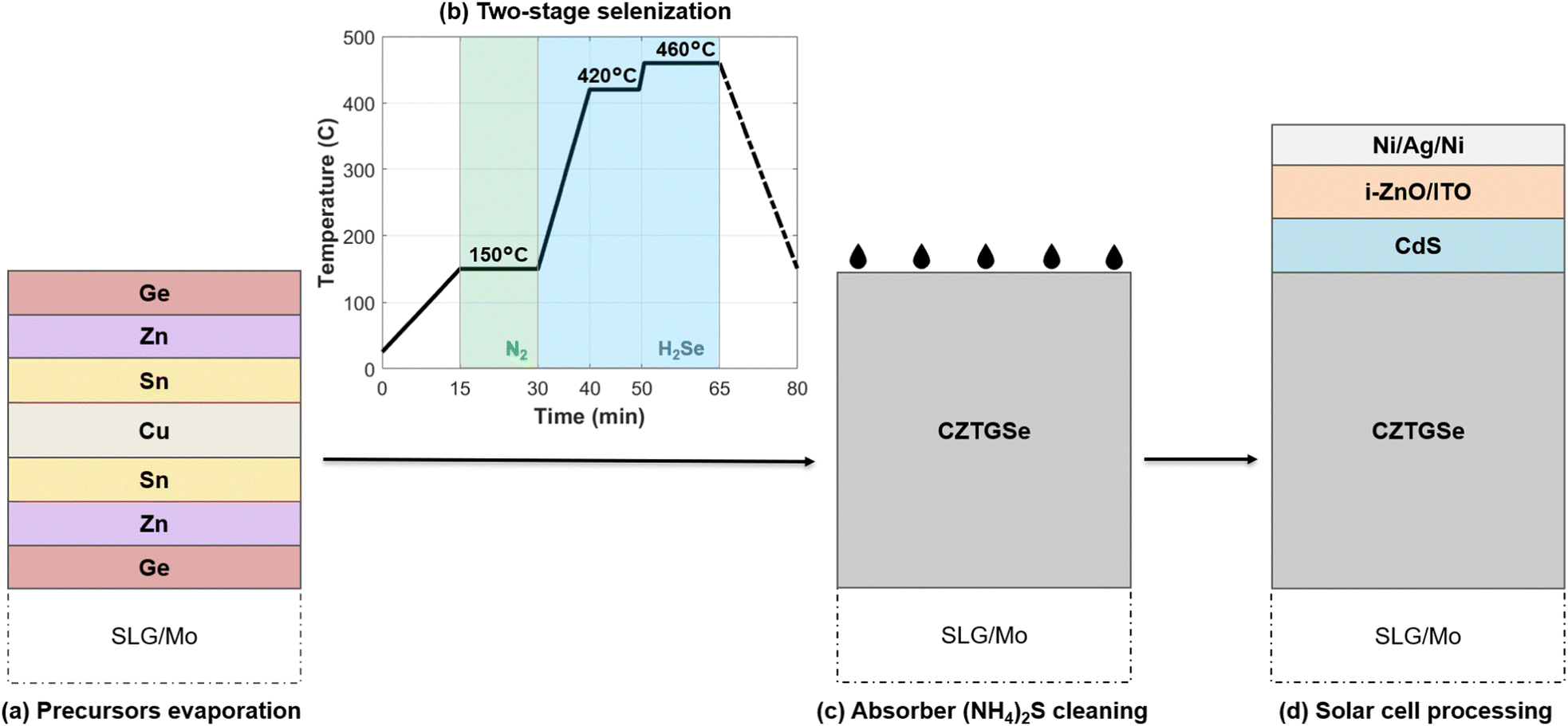 | ||
| Fig. 1 Graphical representation of the complete solar cell processing: (a) e-beam evaporation of the metallic precursor stack on glass/Mo. (b) Temperature profile of the two-step H2Se annealing with pre-annealing in N2. (c) (NH4)2S cleaning treatment applied on the absorber's top surface. (d) Deposition of the CdS buffer, i-ZnO/ITO window layers, and Ag grid to complete the solar cell process. | ||
Preliminary investigations were conducted to optimize the processing recipe. First, regarding the composition, 40% Ge substitution is targeted to approach the efficiency of the reported Sn–Ge bandgap-graded CZTGSe devices.26,27 In contrast to the Cu-poor and Zn-rich stoichiometry usually reported in the literature,2,3,7,8 Cu-poor and Zn-poor composition is preferred herein because previous experiments on Zn-rich absorbers led to high proportions of detrimental ZnSe and consequently poor performance, as reported elsewhere.31 Second, regarding the annealing profile, there are two upgrades introduced in the absorber processing (Fig. 1(b)). On the one hand, the precursor stack is pre-annealed in N2 for 15 minutes at around 150 °C to initiate elemental inter-mixing and favour homogeneity, which impedes bubble formation on the surface. On the other hand, the stack is preliminarily selenized for 10 minutes at 420 °C to mitigate surface defects. Third, previous optimization procedures highlighted the 460 °C selenization temperature as sufficient to ensure kesterite crystalline growth due to the usage of highly reactive H2Se vapour, while guaranteeing the desired absorber morphology.
The synthesized absorbers are further processed by applying a surface treatment procedure in an aqueous solution of (NH4)2S with 6.5–7% sulfur concentration for 30 minutes to remove undesired secondary phases32 (Fig. 1(c)). Then, a 50 nm CdS buffer layer was deposited by chemical bath deposition, a 60 nm i-ZnO and 150 nm indium tin oxide (ITO) window layer was deposited by RF sputtering and a 550 nm Ni/Ag/Ni front grid was deposited by DC sputtering with a shadow mask (Fig. 1(d)). The obtained 5 × 5 cm2 samples are then mechanically scribed to obtain individual cells of 0.5 cm2 area.
Energy dispersive X-ray spectroscopy (EDX BRUKER) measurements are carried out to determine the absorber composition. It is assumed that the EDX results are averaged over the respective elemental penetration depths to around 2 and 1.2 μm for Ge and Sn, respectively, which are close to the absorber thickness of approximately 1.6 μm. However, EDX analysis also considers the studied layers as homogeneous with regard to composition, which is not the case herein as discussed below, and likely induces inaccuracies in the final atomic contents. Raman measurements are performed at an excitation wavelength of 514 nm to detect the presence of kesterite crystalline phases (LabRAM HR Horiba). Steady-state photoluminescence (PL) spectra are measured in a wavelength range from 900 nm to 1300 nm (Picoquant FluoTime 300), with an excitation wavelength of 532 nm (25 ps, 3 MHz). In the present case of bandgap-graded materials, the PL absorption peak is assumed to be located around the minimum optical bandgap where the radiative recombination process requires the least energy. However, higher bandgaps within the absorber may contribute to the PL spectrum.33 At a PL peak wavelength, medium injection time-resolved PL (TRPL) spectroscopy is carried out to extract the minority carrier lifetime by fitting the PL intensity vs. time data to a double-exponential law.34 The focus herein is put on the slow, i.e. longer, lifetime component associated to carrier recombination.35 Time-of-flight secondary ion mass spectrometry (ToF-SIMS) measurements were performed by sputtering the samples with 2 keV O2 ion beam, using 350×350 μm2 sputter area and 100×100 μm2 analysis area. The raw ToF-SIMS data are non-calibrated and thus only provide a qualitative evaluation of the composition. To overcome this in the case of Sn and Ge, their EDX contents in atomic % are matched to their respective total amount of ToF-SIMS counts along the absorber thickness, so as to obtain EDX-calibrated ToF-SIMS results. The precision of this procedure remains affected by the EDX accuracy itself, which is limited by the homogeneity hypothesis discussed above, as well as by the determined absorber boundaries on the ToF-SIMS profile. Current–voltage (IV) measurements are performed using a 4-point probe setup (Keithley 2401 SourceMeter) from −1 V to 1 V, with In iron soldered over the apparent Mo back electrode. An Oriel solar simulator is used to obtain the AM1.5G illumination spectrum for under-light IV. External quantum efficiency (EQE) is measured from 350 to 1300 nm with a 10 nm step using a Bentham PVE300 PV characterization tool. These data are used to extract the electrical bandgap as well as for computing the short-circuit current density Jsc to be compared with the under-light IV results.
3 Results
The SEM pictures taken after selenization and (NH4)2S treatment on the CZTGSe absorbers (Fig. 2(a)) reveal a grain size mostly below the micrometer scale and a relatively smooth surface with sparse defects and intra-grain voids. Similar features can be observed on the cross-section picture, also exhibiting scattered voids at the back contact. EDX composition in Table 1 confirms that the desired Cu-poor and Zn-poor stoichiometry is reached, along with the expected Ge/(Ge + Sn) ratio approaching 40%. The Raman spectrum measured at 514 nm excitation wavelength (Fig. 2(b)) ascertains the polycrystalline kesterite growth through the expected CZTGSe modes at 175, 201, 246 and 276 cm−1, also observed in devices with a comparable Ge/(Ge + Sn) content.17,26,27,31 PL measurements exhibit an absorption maximum at 1195 nm, corresponding to a minimum optical bandgap of 1.04 eV, while the TRPL response indicates a longer carrier lifetime of 1.32 ns (Fig. 2(c)), which appears to be rather poor in comparison with that of other Ge-alloyed kesterite thin films.22,36,37 This is likely the result of recombination,35 especially important at grain boundaries and interfaces where it is assisted by the usually high densities of point defects in kesterites.2–4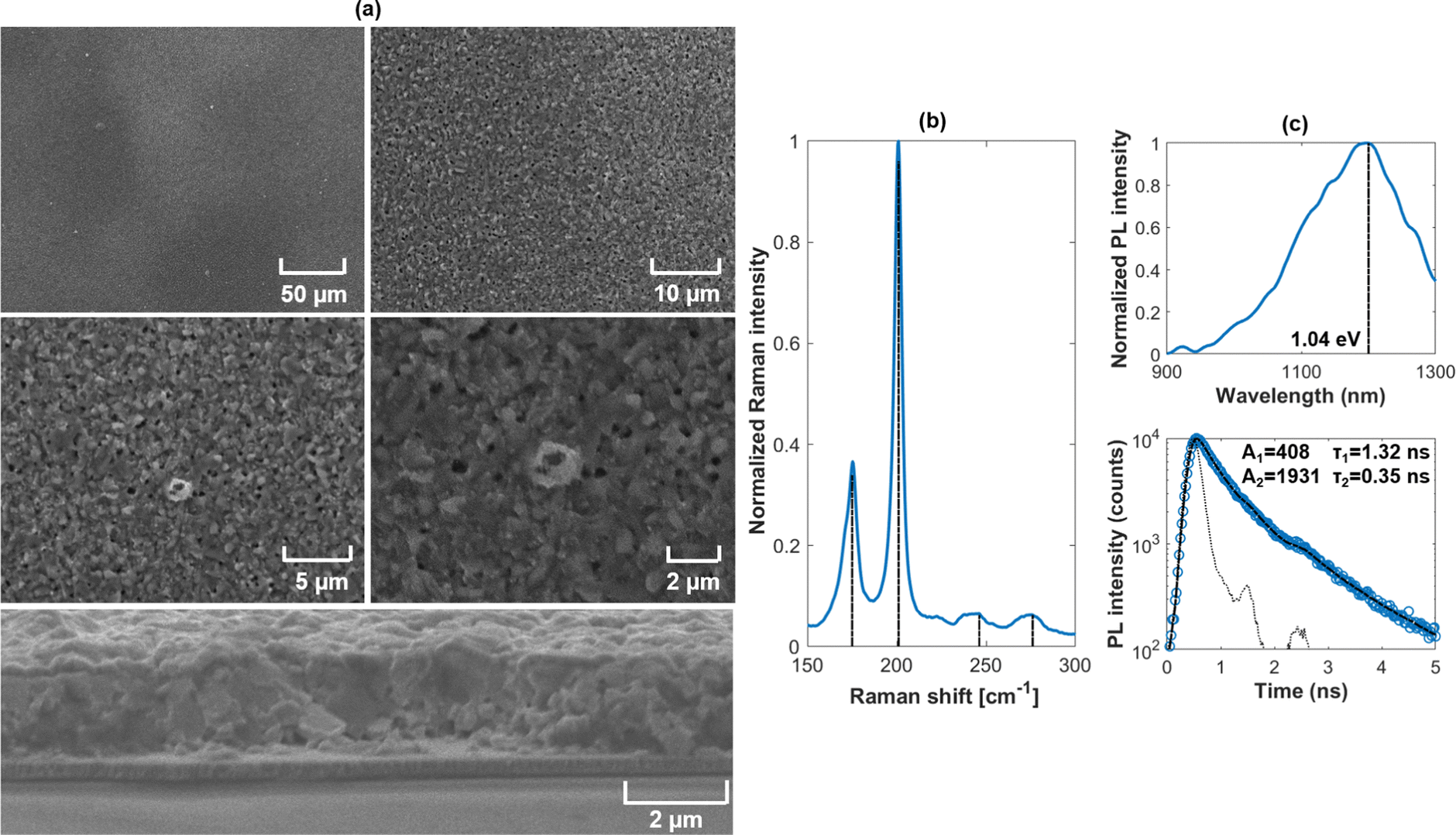 | ||
| Fig. 2 (a) Top surface and cross-sectional scanning electron microscopy (SEM) images of the CZTGSe absorber. (b) Normalized 514 nm Raman spectrum of the CZTGSe absorber with the main kesterite modes at 175, 201, 246 and 276 cm−1. (c) PL spectrum of the CZTGSe absorber exhibiting an absorption peak around 1195 nm, which corresponds to an optical bandgap of 1.04 eV. Double exponential fitting of TRPL measurements provides carrier lifetimes of 1.32 ns and 0.35 ns associated with absolute amplitudes of 408 and 1931, respectively. The little irregularity at 2.5 ns arises from a post-pulse of the pulsed laser used for the measurement. This laser peak shaped together with the rest of the instrument response function (thin black dotted line) is deconvoluted from the experimentally measured decay pulse to yield the fit shown in the graph. The main Raman kesterite modes, PL peak wavelength and carrier lifetime double exponential fitting are highlighted by black dashed lines. | ||
| Elemental composition | EDX data |
|---|---|
| Cu (at%) | 20.60 |
| Zn (at%) | 11.97 |
| Sn (at%) | 9.54 |
| Ge (at%) | 6.87 |
| Se (at%) | 51.01 |
| Cu/(Zn + Sn + Ge) | 0.73 |
| Zn/(Sn + Ge) | 0.73 |
| x = Ge/(Ge + Sn) | 0.42 |
In order to verify the relative evolution of the elemental composition along the CZTGSe absorber thickness and possibly assert the existence of a graded bandgap, ToF-SIMS profiles are measured for the elements of interest (Fig. 3(a)). On the left side, a sharp increase of the In response close to 0 s corresponds to the window layer that was deposited on top with the CdS to protect the absorber surface. On the right side, the upward evolution of the Mo signal beyond 400 s corresponds to the back contact. These two boundaries define the top and back of the CZTGSe absorber, in which Cu, Zn, Ge and Se have apparently diffused towards the back during the processing, while Sn has accumulated at the top surface. The resulting Sn–Ge gradient is claimed to be naturally appearing during the high-temperature annealing step, consequently to the incorporation of Ge within the kesterite lattice and the segregation of SnSe2 near the back contact.16,23,26 It translates into a higher Ge content at the back surface and a higher Sn content at the front surface as shown in Fig. 3(b), via an analogous mechanism to the In–Ga gradient formation in CIGSe.38
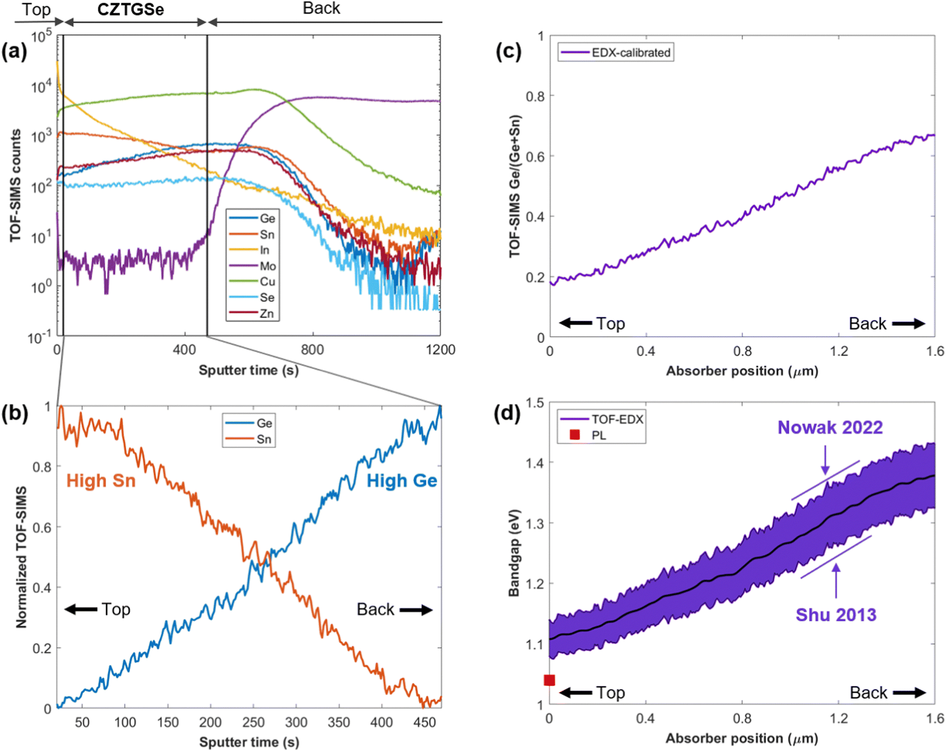 | ||
| Fig. 3 (a) Measured ToF-SIMS counts showing the elemental evolution along the whole CZTGSe absorber and neighbouring layers, with the top and back interfaces illustrated by vertical black solid lines. (b) Normalized ToF-SIMS data for Sn and Ge depicting the Sn–Ge gradient within the CZTGSe absorber. (c) Evolution of the Ge/(Ge + Sn) ratio along the absorber thickness, obtained using the EDX-calibrated ToF-SIMS data. (d) Bandgap profile along the absorber thickness extrapolated from the EDX-calibrated ToF-SIMS data using eqn (1) and (2) as bottom and top boundaries. The mean value between these two limits is depicted with a solid black line, while the PL-extracted minimum bandgap value is shown by a red square symbol. In all figures, the top and back surfaces of the CZTGSe absorbers are highlighted with black solid arrows. | ||
Quantifying the x = Ge/(Ge + Sn) ratio along the absorber thickness is especially interesting since it can be used to determine the bandgap of CZTGSe absorbers through the conduction band energy variation,21 using an empirical formula that relies on the bowing parameter b:
| Eg,CZTGSe(x) = (1 − x) × Eg,CZTSe + x × Eg,CZGSe − b × x × (1 − x), | (1) |
| Eg,CZTGSe(x) = 1.03 + 0.6 × x. | (2) |
To quantitatively assert the profile of x within the CZTGSe absorber, an EDX-based calibration is performed as described in Section 2 and a curve is obtained as shown in Fig. 3(c). Since the above equations state that lower x ratios induce lower bandgap values, the TOF-EDX profile shown in Fig. 3(c) suggests that the bandgap is increasing towards the back of CZTGSe whereas it is minimum at the top surface. Following the discussion in Section 2, this minimum bandgap at the front arguably corresponds to a PL bandgap of 1.04 eV (Fig. 2(c)). The 70 meV discrepancy between the PL-extracted optical bandgap and the TOF-EDX composition-extrapolated electric bandgap is likely explained by the large band tails typically affecting kesterite materials. This induces a significant shift of the PL absorption peak, leading to an underestimation of the electric bandgap by up to 100 meV.39 Eventually, from the TOF-EDX-calibrated profile of x, the bandgap can be estimated along the absorber thickness using eqn (1) and (2), respectively, as lower and upper boundaries of Eg,CZTGSe(x) shown in Fig. 3(d). This mainly serves to demonstrate the existence of bandgap grading within the CZTGSe absorber, rather than to provide an exact bandgap profile, and the accuracy of which is limited by the ToF-SIMS calibration procedure using EDX.
Eventually, using these CZTGSe absorbers, complete solar cells are fabricated following the procedure given in Section 2, and their IV characteristics under light and in the dark are measured as shown for the champion cell in Fig. 4(a). The corresponding performance figures-of-merit are the efficiency η in %, the open-circuit voltage Voc in mV, the short-circuit current density Jsc in mA cm−2 and the fill factor FF in %, shown in Table 2 along with parasitic resistances Rsh and Rs. The EQE data shown in Fig. 4(b) enable a second estimation of both Jsc and the bandgap Eg, by integration over the AM1.5G solar spectrum and extrapolation from the peak wavelength of the derivative, respectively, also provided in Table 2. It appears that the value of Jsc extracted from light-IV characteristics is overestimated by roughly 5% as compared to the EQE results. The discrepancy between the bandgaps estimated using EQE (1.23 eV) and PL (1.04 eV) is much more significant, with an absolute difference of 190 meV. This is likely the result of high crystalline disorder and bulk defect-induced bandgap fluctuations in the kesterite absorber, as observed elsewhere.39 The collapse in EQE within the 650–900nm range (blue lines in Fig. 4(b)) is arguably a sign of hindered charge collection within the absorber, likely also the consequence of the numerous point defects inside the kesterite lattice.
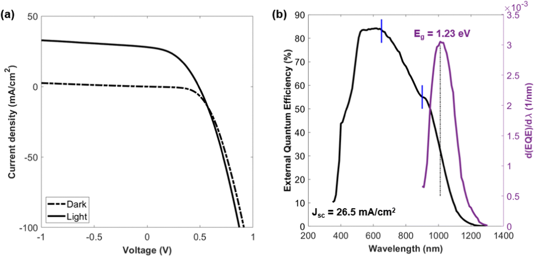 | ||
| Fig. 4 (a) Champion cell IV curves in the dark (dashed line) and under AM1.5G illumination (solid line). (b) EQE response of the champion CZTGSe cell at 0 V, in black solid line (left vertical axis), and its derivative with respect to wavelength in the purple solid line (right vertical axis). The Jsc and Eg values, respectively, extrapolated from the AM1.5G spectral integration and the EQE derivative peak position, are indicated. The dashed black line and blue solid lines are a guide to the eye, respectively, highlighting the peak position of d(EQE)/dλ and the hindered carrier collection within the absorber. | ||
| Sample | CZTGSe |
|---|---|
| η (%) | 6.0 |
| V oc (mV) | 487 |
| J sc (mA cm−2) | 28.1 (26.5) |
| FF (%) | 43.7 |
| R s (Ω cm2) | 1.6 |
| R sh (Ω cm2) | 555 |
| η c (%) | 6.8 |
| FFc (%) | 48.9 |
| E g (eV) | 1.23 |
Considering the bandgap of 1.23 eV obtained from EQE, this champion cell reaches about 70% of its Shockley–Queisser (SQ) limit in terms of Jsc,40,41 which could be improved by reducing parasitic absorption of upper layers in the red light region as well as mitigating electronic defects as mentioned above. This latter issue likely also contributes to the large Voc SQ deficit of 50% affecting the studied devices and kesterites more generally. Indeed, reports of kesterite solar cells with higher efficiencies also demonstrate restrained Voc values rather close to the one observed here,17,26,36,42,43 even for the present world record devices.6 Thus, this generalized limitation of Voc for kesterite PV absorbers still needs to be tackled. Overall, the presented champion CZTGSe device exhibits encouraging Voc and Jsc values, respectively, close to 500 mV and 30 mA cm−2, slightly below those reported in the literature with equivalent absorber composition.17,26,36,42,43 Therefore, the main issue appears to be the largely degraded fill factor as compared to other studies.17,26,36,42,43 More precisely, for the champion cell, the FF does not exceed 45% even though the values of Rsh and Rs, respectively, approach 500 Ω cm2 and 2 Ω cm2, which are of the same order of magnitude as that for kesterite devices with higher fill factors and efficiencies.16,26,36,42–46 This suggests that loss mechanisms other than Rsh and Rs contribute in parallel to the poor FF observed herein. Such a trend is emphasized by the fill factor remaining relatively low after parasitic correction, i.e. FFc below 50% shown in Table 2, contrary to other CZTGSe devices showing FF values around 65% for comparable Rsh and/or Rs.9,16,19,42,45 In this regard, further studies are needed to understand the physical loss mechanisms responsible for the low fill factor of these CZTGSe solar cells.
Besides this, further experiments are required to accurately determine the role played by the bandgap gradient in the CZTGSe absorbers developed in this work, since it arguably boosts carrier collection according to other reports on CIGSe1 and CZTG(S)Se solar cells.16,26,27 The statistical dispersion of the IV parameters between different cells from this process is illustrated in Fig. 5, revealing a relatively large spread for all figures-of-merit, thus highlighting the room for improvement in terms of reproducibility. Eventually, preliminary experiments were conducted to incorporate low amounts of sulfur into these absorbers and evaluate the effect on the lifetime and performance. The additional sulfurization of the CZTGSe layers did not lead to substantial changes with regard to the PL response and lifetime but rather degraded the IV performance, as shown in the Supplementary Fig. S1 (ESI†).
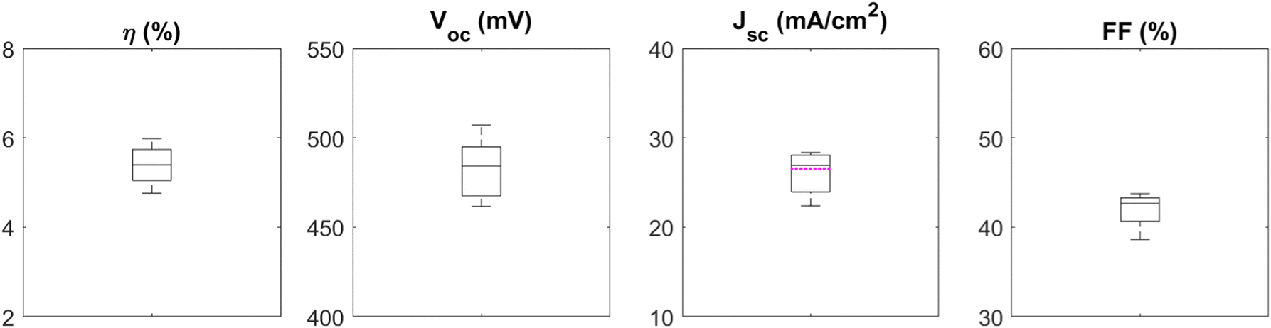 | ||
| Fig. 5 Statistical dispersion of η, Voc, Jsc and FF for the CZTGSe solar cells. The Jsc value extracted from the EQE data of the champion cell is shown in the pink dashed line, revealing a slight overestimation of Jsc extracted from under light IV. For each box, the central line represents the median, while its top and bottom edges, respectively, indicate the 25th and 75th percentiles. The whiskers, i.e. the dashed lines extending from both edges of each box, indicate the most extreme data points. | ||
4 Conclusions
To conclude, an optimized sequential process based on N2 pre-annealing and two-stage H2Se high-temperature annealing is presented to deposit Sn–Ge bandgap-graded polycrystalline CZTGSe thin-film absorbers. These absorbers exhibit micron-size grains with an acceptable morphology and a slightly defective surface, but a limited carrier lifetime. A champion efficiency of 6% is achieved, with encouraging Jsc values close to 30 mA cm−2 reaching around 70% of their Shockley–Queisser limit. The large Voc deficit is likely due to high densities of electronic defects usually affecting kesterite compounds, for which a solution still needs to be found. The other main performance limitation is the low fill factor, apparently not only caused by parasitic resistances. Future enhancements require a deeper understanding of the loss mechanisms at stake in parallel with supplementary experiments to gauge the impact of the demonstrated bandgap grading design, which is a remarkable feature of Ge inclusion within kesterite solar cells.Author contributions
Conceptualization, R. S. and G. B.; methodology, R. S., G. B., Y. W., A. U. Z., and K. S.; software, R. S. and G. B.; validation, R. S. and G. B.; formal analysis, R. S. and G. B.; investigation, R. S., G. B., Y. W., A. U. Z., and K. S.; resources, R. S. and G. B.; data curation, R. S.; writing – original draft preparation, R. S.; Writing – review and editing, R. S., G. B., J. d. W, D. F. and B. V.; visualization, R. S.; supervision, G. B., D. F. and B. V.; project administration, G. B. and B. V.; and funding acquisition, R. S., G. B. and B. V.Conflicts of interest
There are no conflicts to declare.Acknowledgements
This work has received funding from the European Union's Horizon 2020 research and innovation programme under grant agreement 952982 (CUSTOM-ART project). R.S. thanks FWO for the funding through the Fundamental Research PhD Fellowship (1178022N).References
- G. M. Wilson, M. Al-Jassim, W. K. Metzger, S. W. Glunz, P. Verlinden, G. Xiong, L. M. Mansfield, B. J. Stanbery, K. Zhu, Y. Yan, J. J. Berry, A. J. Ptak, F. Dimroth, B. M. Kayes, A. C. Tamboli, R. Peibst, K. Catchpole, M. O. Reese, C. S. Klinga, P. Denholm, M. Morjaria, M. G. Deceglie, J. M. Freeman, M. A. Mikofski, D. C. Jordan, G. TamizhMani and D. B. Sulas-Kern, J. Phys. D: Appl. Phys., 2020, 53, 493001 CrossRef CAS.
- M. He, C. Yan, J. Li, M. P. Suryawanshi, J. Kim, M. A. Green and X. Hao, Adv. Sci., 2021, 8, 2004313 CrossRef CAS PubMed.
- K. J. Tiwari, S. Giraldo, M. Placidi, Z. Jehl Li-Kao and E. Saucedo, in Recent Advances in Thin Film Photovoltaics, ed. U. P. Singh and N. B. Chaure, Springer Nature, Singapore, 2022, pp. 41–66 Search PubMed.
- S. Giraldo, Z. Jehl, M. Placidi, V. Izquierdo-Roca, A. Pérez-Rodríguez and E. Saucedo, Adv. Mater., 2019, 31, 1806692 CrossRef PubMed.
- M. A. Green, E. D. Dunlop, G. Siefer, M. Yoshita, N. Kopidakis, K. Bothe and X. Hao, Prog. Photovoltaics, 2023, 31, 3–16 Search PubMed.
- Y. Gong, Q. Zhu, B. Li, S. Wang, B. Duan, L. Lou, C. Xiang, E. Jedlicka, R. Giridharagopal, Y. Zhou, Q. Dai, W. Yan, S. Chen, Q. Meng and H. Xin, Nat. Energy, 2022, 7, 966–977 CrossRef CAS.
- T. Gershon, D. Bishop, P. Antunez, S. Singh, K. W. Brew, Y. S. Lee, O. Gunawan, T. Gokmen, T. Todorov and R. Haight, Curr. Opin. Green Sustainable Chem., 2017, 4, 29–36 CrossRef.
- Y. E. Romanyuk, S. G. Haass, S. Giraldo, M. Placidi, D. Tiwari, D. J. Fermin, X. Hao, H. Xin, T. Schnabel, M. Kauk-Kuusik, P. Pistor, S. Lie and L. H. Wong, J. Phys. Energy, 2019, 1, 044004 CrossRef CAS.
- Y. Deng, Z. Zhou, X. Zhang, L. Cao, W. Zhou, D. Kou, Y. Qi, S. Yuan, Z. Zheng and S. Wu, J. Energy Chem., 2021, 61, 1–7 CrossRef CAS.
- Z. Zhang, Q. Gao, J. Guo, Y. Zhang, Y. Han, J. Ao, M.-J. Jeng, F. Liu, W. Liu and Y. Zhang, Sol. RRL, 2020, 4, 2000059 CrossRef CAS.
- J. Wang, J. Zhou, X. Xu, F. Meng, C. Xiang, L. Lou, K. Yin, B. Duan, H. Wu, J. Shi, Y. Luo, D. Li, H. Xin and Q. Meng, Adv. Mater., 2022, 34, 2202858 CrossRef CAS PubMed.
- K. Biswas, S. Lany and A. Zunger, Appl. Phys. Lett., 2010, 96, 201902 CrossRef.
- H. Nishihara, T. Maeda, A. Shigemi and T. Wada, Jpn. J. Appl. Phys., 2017, 56, 04CS08 CrossRef.
- T. Ratz, N. D. Nguyen, G. Brammertz, B. Vermang and J.-Y. Raty, J. Mater. Chem. A, 2022, 10, 4355–4365 RSC.
- S. Giraldo, E. Saucedo, M. Neuschitzer, F. Oliva, M. Placidi, X. Alcobé, V. Izquierdo-Roca, S. Kim, H. Tampo, H. Shibata, A. Pérez-Rodríguez and P. Pistor, Energy Environ. Sci., 2018, 11, 582–593 RSC.
- J. Liu, Z. Liu, K. Gao, H. Cai, Y. Liu, W. Zhao, X. Liu, K. Cheng and Z. Du, ACS Appl. Mater. Interfaces, 2021, 13, 56302–56308 CrossRef CAS PubMed.
- D. Nowak, T. Khonsor, D. Pareek and L. Gütay, Appl. Sci., 2022, 12, 1376 CrossRef CAS.
- S. Padhy, V. Kumar, N. B. Chaure and U. P. Singh, Mater. Sci. Semicond. Process., 2022, 138, 106276 CrossRef CAS.
- M. Neuschitzer, M. E. Rodriguez, M. Guc, J. A. Marquez, S. Giraldo, I. Forbes, A. Perez-Rodriguez and E. Saucedo, J. Mater. Chem. A, 2018, 6, 11759–11772 RSC.
- J. González-Castillo, F. Pulgarín-Agudelo, E. Rodríguez-González, O. Vigil-Galán, M. Courel-Piedrahita and J. Andrade-Arvizu, Mater. Sci. Semicond. Process., 2018, 83, 96–101 CrossRef.
- Q. Shu, J.-H. Yang, S. Chen, B. Huang, H. Xiang, X.-G. Gong and S.-H. Wei, Phys. Rev. B: Condens. Matter Mater. Phys., 2013, 87, 115208 CrossRef.
- S. Kim, K. M. Kim, H. Tampo, H. Shibata and S. Niki, Appl. Phys. Express, 2016, 9, 102301 CrossRef.
- J. Márquez, H. Stange, C. J. Hages, N. Schaefer, S. Levcenko, S. Giraldo, E. Saucedo, K. Schwarzburg, D. Abou-Ras, A. Redinger, M. Klaus, C. Genzel, T. Unold and R. Mainz, Chem. Mater., 2017, 29, 9399–9406 CrossRef.
- B. Vermang, G. Brammertz, M. Meuris, T. Schnabel, E. Ahlswede, L. Choubrac, S. Harel, C. Cardinaud, L. Arzel, N. Barreau, J. van Deelen, P.-J. Bolt, P. Bras, Y. Ren, E. Jaremalm, S. Khelifi, S. Yang, J. Lauwaert, M. Batuk, J. Hadermann, X. Kozina, E. Handick, C. Hartmann, D. Gerlach, A. Matsuda, S. Ueda, T. Chikyow, R. Félix, Y. Zhang, R. G. Wilks and M. Bär, Sustainable Energy Fuels, 2019, 3, 2246–2259 RSC.
- S. Khelifi, G. Brammertz, L. Choubrac, M. Batuk, S. Yang, M. Meuris, N. Barreau, J. Hadermann, H. Vrielinck, D. Poelman, K. Neyts, B. Vermang and J. Lauwaert, Sol. Energy Mater. Sol. Cells, 2021, 219, 110824 CrossRef CAS.
- J. Andrade-Arvizu, R. Fonoll-Rubio, Y. Sánchez, I. Becerril-Romero, C. Malerba, M. Valentini, L. Calvo-Barrio, V. Izquierdo-Roca, M. Placidi, O. Vigil-Galán, A. Pérez-Rodríguez, E. Saucedo and Z. Jehl Li-Kao, ACS Appl. Energy Mater., 2020, 3, 10362–10375 CrossRef CAS.
- J. Fu, D. Kou, W. Zhou, Z. Zhou, S. Yuan, Y. Qi and S. Wu, J. Mater. Chem. A, 2020, 8, 22292–22301 RSC.
- M. Buffière, H. ElAnzeery, S. Oueslati, K. Ben Messaoud, G. Brammertz, M. Meuris and J. Poortmans, Thin Solid Films, 2015, 582, 171–175 CrossRef.
- T. Kohl, G. Brammertz, J. de Wild, M. Neuwirth, M. Meuris, J. Poortmans and B. Vermang, Thin Solid Films, 2018, 660, 247–252 CrossRef CAS.
- G. Brammertz, T. Kohl, J. De Wild, M. Meuris, B. Vermang and J. Poortmans, Thin Solid Films, 2019, 670, 76–79 CrossRef CAS.
- A. Ruiz-Perona, Y. Sánchez, M. Guc, L. Calvo-Barrio, T. Jawhari, J. Merino, M. León and R. Caballero, Sol. Energy, 2020, 199, 864–871 CrossRef CAS.
- L. Choubrac, M. Bär, X. Kozina, R. Félix, R. G. Wilks, G. Brammertz, S. Levcenko, L. Arzel, N. Barreau, S. Harel, M. Meuris and B. Vermang, ACS Appl. Energy Mater., 2020, 3, 5830–5839 CrossRef CAS.
- J. de Wild, D. G. Buldu, T. Kohl, G. Birant, G. Brammertz, M. Meuris, J. Poortmans and B. Vermang, J. Appl. Phys., 2020, 128, 163102 CrossRef CAS.
- R. K. Ahrenkiel, Solid-State Electron., 1992, 35, 239–250 CrossRef CAS.
- A. Kanevce, D. H. Levi and D. Kuciauskas, Prog. Photovolt: Res. Appl., 2014, 22, 1138–1146 CrossRef CAS.
- S. Bag, O. Gunawan, T. Gokmen, Y. Zhu and D. B. Mitzi, Chem. Mater., 2012, 24, 4588–4593 CrossRef CAS.
- C. J. Hages, S. Levcenco, C. K. Miskin, J. H. Alsmeier, D. Abou-Ras, R. G. Wilks, M. Bär, T. Unold and R. Agrawal, Prog. Photovolt: Res. Appl., 2015, 23, 376–384 CrossRef CAS.
- R. Mainz, A. Weber, H. Rodriguez-Alvarez, S. Levcenko, M. Klaus, P. Pistor, R. Klenk and H.-W. Schock, Prog. Photovolt: Res. Appl., 2015, 23, 1131–1143 CrossRef CAS.
- S. Siebentritt, G. Rey, A. Finger, D. Regesch, J. Sendler, T. P. Weiss and T. Bertram, Sol. Energy Mater. Sol. Cells, 2016, 158, 126–129 CrossRef CAS.
- W. Shockley and H. J. Queisser, J. Appl. Phys., 1961, 32, 510–519 CrossRef CAS.
- S. Rühle, Sol. Energy, 2016, 130, 139–147 CrossRef.
- C. Gao, Y. Sun and W. Yu, Coatings, 2018, 8, 304 CrossRef.
- S. Kim, K. M. Kim, H. Tampo, H. Shibata, K. Matsubara and S. Niki, Sol. Energy Mater. Sol. Cells, 2016, 144, 488–492 CrossRef CAS.
- A. D. Collord and H. W. Hillhouse, Chem. Mater., 2016, 28, 2067–2073 CrossRef CAS.
- Y. Sun, L. Du, Z. Liu, W. Ding, C. Gao and W. Yu, Mater. Lett., 2017, 195, 76–78 CrossRef CAS.
- S. Lee, K. J. Price, E. Saucedo and S. Giraldo, Sol. Energy, 2019, 194, 114–120 CrossRef CAS.
Footnote |
| † Electronic supplementary information (ESI) available: PL and IV experiments on selenized-sulfurized CZTGSSe absorbers. See DOI: https://doi.org/10.1039/d3ya00359k |
| This journal is © The Royal Society of Chemistry 2023 |