
 Open Access Article
 This Open Access Article is licensed under a
 Creative Commons Attribution 3.0 Unported Licence
Electrostatic modulation of thermoelectric transport properties of 2H-MoTe2†
Tianhui
Zhu‡
 a,
Sree Sourav
Das
a,
Safoura
Nayeb Sadeghi
b,
Farjana Ferdous
Tonni
a,
Sergiy
Krylyuk
c,
Costel
Constantin
d,
Keivan
Esfarjani
bef,
Albert V.
Davydov
c and
Mona
Zebarjadi
*ae
a,
Sree Sourav
Das
a,
Safoura
Nayeb Sadeghi
b,
Farjana Ferdous
Tonni
a,
Sergiy
Krylyuk
c,
Costel
Constantin
d,
Keivan
Esfarjani
bef,
Albert V.
Davydov
c and
Mona
Zebarjadi
*ae
aDepartment of Electrical and Computer Engineering, University of Virginia, Charlottesville, Virginia 22904, USA. E-mail: m.zebarjadi@virginia.edu
bDepartment of Mechanical and Aerospace Engineering, University of Virginia Charlottesville, Virginia 22904, USA
cMaterials Science and Engineering Division, National Institute of Standards and Technology, Gaithersburg, Maryland 20899, USA
dDepartment of Physics and Astronomy, James Madison University, Harrisonburg, Virginia 22807, USA
eDepartment of Materials Science and Engineering, University of Virginia, Charlottesville, Virginia 22904, USA
fDepartment of Physics, University of Virginia, Charlottesville, Virginia 22904, USA
First published on 27th September 2023
Abstract
Two-dimensional layered transition metal dichalcogenides are potential thermoelectric candidates with application in on-chip integrated nanoscale cooling and power generation. Here, we report a comprehensive experimental and theoretical study on the in-plane thermoelectric transport properties of thin 2H-MoTe2 flakes prepared in field-effect transistor geometry to enable electrostatic gating and modulation of the electronic properties. The thermoelectric power factor is enhanced by up to 45% using electrostatic modulation. The in-plane thermal conductivity of 9.8 ± 3.7 W m−1 K−1 is measured using the heat diffusion imaging method in a 25 nm thick flake. First-principles calculations are used to obtain the electronic band structure, phonon band dispersion, and electron–phonon scattering rates. The experimental electronic properties are in agreement with theoretical results obtained within energy-dependent relaxation time approximation. The thermal conductivity is evaluated using both the relaxation time approximation and the full iterative solution to the phonon Boltzmann transport equation. This study establishes a framework to quantitively compare first-principle-based calculations with experiments in 2D layered materials.
Introduction
In recent years, there has been growing research interest in 2D thermoelectric materials.1 Thermoelectric modules can convert thermal energy to electricity or use electricity for heat management. The thermoelectric power factor is defined as PF = σS2, where σ is the electrical conductivity and S is the Seebeck coefficient, . Seebeck effect describes how much voltage difference (ΔV) can be generated with a temperature difference (ΔT) and is the basis of thermoelectric power generation. Power factor times temperature (PFT) is also often used since it shares the same unit as thermal conductivity, k. The efficiency of thermoelectric energy conversion is an increasing function of the thermoelectric figure of merit,
  .
.
With the continued miniaturization of modern electronics, the dissipated power density keeps increasing.2 2D materials are great candidates for nanoscale power generation to recycle waste heat and for hot spot cooling due to their nanometer thicknesses. They often possess unique chemical, mechanical, and physical properties compared to their bulk counterparts.3,4 As a result of the small thickness, the Fermi level and the charge carrier concentrations of 2D materials can be tuned by electrostatic gating using the electric field effect.5 This is an advantage over bulk materials as it avoids chemical doping processes and allows real-time Fermi-level tuning and optimization of the thermoelectric figure of merit using a single sample. For example, monolayer graphene on hexagonal boron nitride (hBN) has been shown to have a PFT as high as 10.35 W m−1 K−1 at room temperature under the optimal back gate bias,6 which is one order of magnitude higher than that of commercial thermoelectric material, bulk Bi2Te3. Graphene also has a high thermal conductivity on the order of 1000 W m−1 K−1. While this makes graphene an excellent candidate for active cooling purposes,7–9 where passive cooling by phonon transport works together with active cooling by the Peltier effect to conduct heat away from the hot spots, it also means that its ZT is not as appealing for thermoelectric energy conversion applications.
For conventional energy conversion applications, we turn to 2D transition metal dichalcogenides (TMDs). They possess a wide range of tunable electronic properties (from insulating to superconducting) and a relatively low thermal conductivity (much smaller than graphene), which may result in high ZT values. High ZT requires a large Seebeck coefficient, high electrical conductivity, and low thermal conductivity. At the same time, the interplay between these transport parameters means that ZT enhancement is complex: for example, the higher carrier concentration is beneficial for higher electrical conductivity but leads to lower Seebeck coefficient values. The intricate balance usually occurs in highly doped semiconductors10 or possibly semimetals.11
2D semiconductor MoS2 has been studied extensively for thermoelectric applications and the best-performing samples showed a PFT close to 2.5 W m−1 K−1 with high mobility of 60 cm2 V−1 s−1 (bilayer on SiO2 at room temperature)12 and up to 350 cm2 V−1 s−1 (six layers on hBN at 50 K).13 This large PFT has been achieved following years of continued research effort. In 2014, a large Seebeck coefficient of −30 mV K−1 was reported for CVD-grown monolayer MoS2; the power factor, however, was small due to low conductance.14 Two years after this, bilayer MoS2 was shown to have a Seebeck coefficient of −450 μV K−1 and a power factor of 1.5 W m−1 K−1.15 Characterization of the in-plane thermal conductivity of many 2D materials is challenging due to their small sample dimensions. In the case of MoS2, there have been large discrepancies depending on the sample qualities and the experimental techniques. Even with the same Raman spectroscopy-based technique, reported values were between 35 and 85 W m−1 K−1 for monolayer MoS2,16–19 where the sample absorption coefficient and the sample quality were expected to play a significant role. The thermal bridge method had a thermal conductivity of few-layer MoS2 at about 45 W m−1 K−1![[thin space (1/6-em)]](https://www.rsc.org/images/entities/char_2009.gif) 20 and monolayer MoS2 at 24 W m−1 K−1.21 Molecular dynamics calculations revealed thermal conductivity of 117 W m−1 K−1 for suspended monolayers and 31 W m−1 K−1 for supported samples.22 As sample quality also affects carrier mobility and transport performance, these large uncertainties make it less plausible to estimate ZT by combining PFT and k across different studies.
20 and monolayer MoS2 at 24 W m−1 K−1.21 Molecular dynamics calculations revealed thermal conductivity of 117 W m−1 K−1 for suspended monolayers and 31 W m−1 K−1 for supported samples.22 As sample quality also affects carrier mobility and transport performance, these large uncertainties make it less plausible to estimate ZT by combining PFT and k across different studies.
2H-MoTe2 is another semiconducting molybdenum-based TMD material with an indirect gap of 0.83 eV in the bulk form and a direct gap of 1.1 eV in the monolayer limit.23,24 Most of the research on MoTe2 has been focused on electronic25–28 and optoelectronic26,29 applications whereas the studies of its thermoelectric properties are limited. Seebeck coefficient of n-type single crystal bulk MoTe2 was measured to be around −400 μV K−1 from 77 K to 300 K.30 At room temperature, its electrical conductivity was about 750 S m−1 and its PFT was 0.036 W m−1 K−1.30 A 330 nm thick 2H-MoTe2 thin film prepared by magnetron co-sputtering showed a p–n type transition with increasing temperature, giving a maximum PFT of 0.15 W m−1 K−1 at 460 K for p-type conduction and 0.55 W m−1 K−1 at 670 K for n-type conduction.31 At room temperatures, the sample was p-type with σ = 1.5 × 10⁻⁴ S m−1, S = 25 μV K−1 and a PFT of 0.0028 W m−1 K−1.31 The enhancement in PFT at higher temperature was a result of increased Seebeck coefficient values with increasing conductivity, which was unusual and was attributed to improved mobility. Investigations of the thermal conductivity of MoTe2 are also very limited. Yan et al. determined the c-axis thermal conductivity of MoTe2 as 1.5 W m−1 K−1 at 300 K using time-domain thermoreflectance (TDTR) method.32 DFT calculations estimated the in-plane lattice thermal conductivity of monolayer MoTe2 to be around 60 W m−1 K−1 at room temperature.33 These studies indicate that 2H-MoTe2 can be a potential candidate for thermoelectrics, especially in the few-layer limit when the band structure changes due to quantum confinement and the chemical potential can be tuned by the gate voltage.
In this manuscript, we report a comprehensive experimental and theoretical study of room-temperature in-plane thermoelectric transport in thin 2H-MoTe2 flakes. Electrical conductivity and Seebeck coefficient are measured as a function of the back gate bias. Further understanding of the electrical transport data is provided by first-principles calculations with energy-dependent relaxation times, by considering electron–phonon scattering and ionized impurity scattering. Thermal conductivity is also reported, which, to the best of our knowledge, is the first in-plane thermal transport characterization of thin MoTe2. Due to the difficulty in measuring the thermal conductivity of thin 2D films, most of the literature reports only the power factor. The thermal conductivity measurements enable us to estimate ZT as well as to provide a more complete evaluation of the MoTe2 material in terms of thermoelectric applications. In-plane thermal conductivity of bulk MoTe2 is also calculated within both the relaxation time approximation and the full iterative solution to the phonon Boltzmann equation, and compared to the experimental data.
Materials and methods
MoTe2 crystals were grown by the Chemical Vapor Transport (CVT) method using polycrystalline MoTe2 charge and iodine transport agent. The growth was conducted in a vacuum-sealed quartz ampoule at 970 °C for 7 d followed by a 3 d annealing at 800 °C to stabilize the hexagonal 2H phase. Phase purity was confirmed by powder X-ray diffraction measurements and the data are included in the ESI† (see Fig. S1).Device fabrication
Thin 2H-MoTe2 flakes were exfoliated onto 300 nm SiO2/p+-Si substrates by the Scotch tape method. The substrates were pre-cleaned by acetone and isopropanol sonication, followed by annealing at 400 °C in forming gas (5% H2/95% Ar) to remove chemical residues. Flakes with a uniform thickness were chosen under an optical microscope. The thickness of the exfoliated flakes was characterized by a Bruker Dimension Icon atomic force microscope (AFM) and was around 25 nm for the two devices used for room temperature tests and 90 nm for the thicker flake used for low-temperature thermal conductivity measurement. AFM data are shown in Fig. S3 (ESI†). The standard thermoelectric electrode patterns were prepared using laser lithography (385 nm), which includes one heater, two thermometers, and two side contacts, see inset in Fig. 1 for the geometry of the device. 5 nm Ti and 100 nm Au were evaporated as contact metals (base pressure <10−5 Torr, 1 Å s−1). The shape of each flake was identified under a microscope and subsequently etched to a rectangular shape by opening etch windows with laser lithography and then reactive ion etching (RIE) with SF6 (30 W) for up to 1 min. Exposure to air during the fabrication process might cause some surface oxidation, but the oxidation is known only to occur in the top two or three layers near the surface and the bulk of the flake remains intact.34 The samples were kept inside an argon-filled glovebox and annealed in a high vacuum (∼10−6 Torr) at 325 °C for 30 min in the cryostat immediately before measurements to minimize effects from environmental contamination.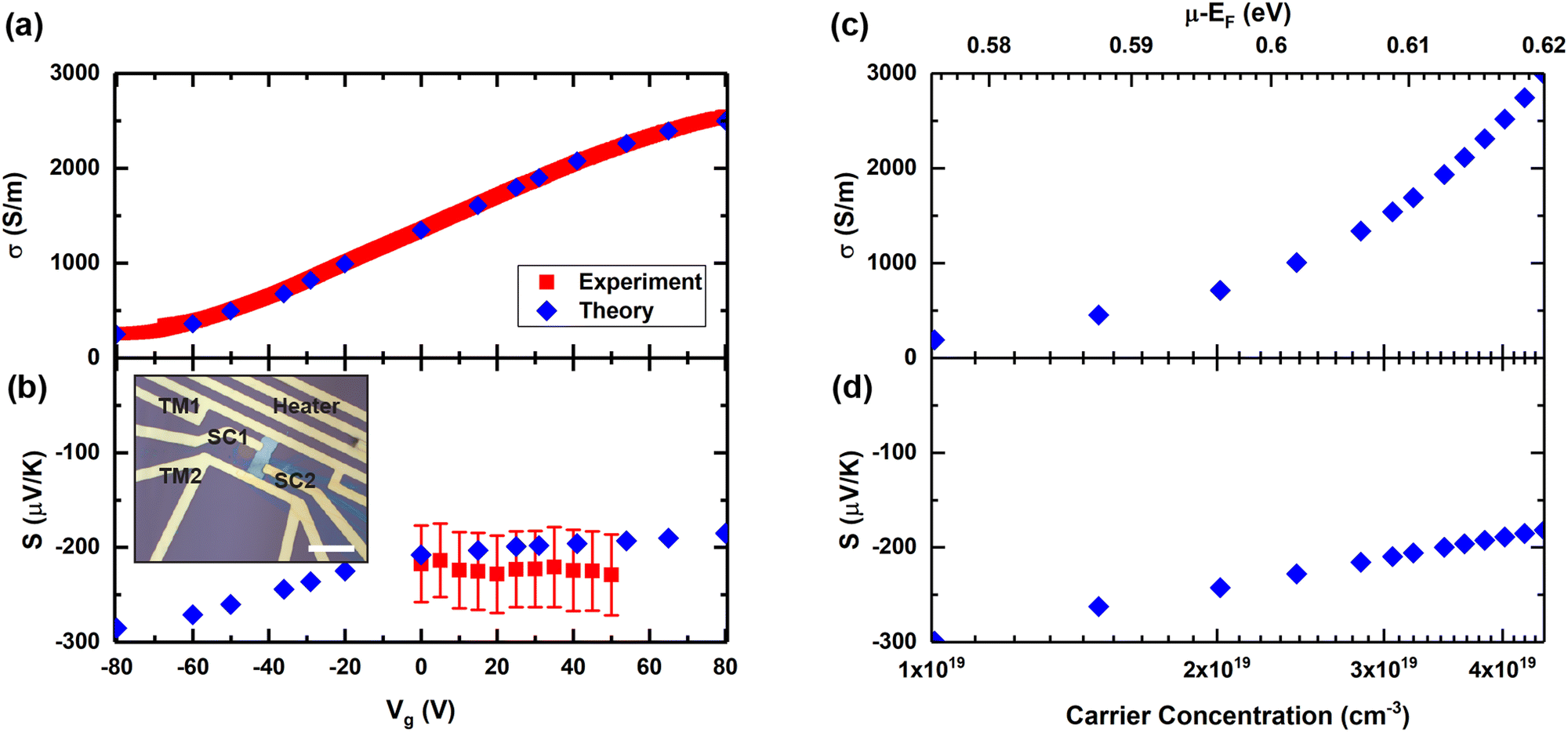 | ||
| Fig. 1 Experimental (a) electrical conductivity and (b) Seebeck coefficient of the exfoliated thin MoTe2 sample as a function of the gate voltage, compared with theoretically obtained values. Calculated (c) electrical conductivity and (d) Seebeck coefficients as a function of the carrier concentration (bottom axis) and the chemical potential with respect to the intrinsic Fermi level, μ–EF (top axis). The inset in (c) shows an optical image of the device, with the heater, the thermometers (TMs) and the side contacts (SC) noted. The scale bar is 20 μm. | ||
Measurement setup
The electrical transport measurements were performed in a JANIS cryostat system customized for transport measurements in a high vacuum (∼10−6 Torr). A Keithley 2401 SourceMeter was used to measure the four-probe resistance under 1 μA current. Back gate voltage, Vg, was applied to the highly doped Si substrate using a Keithley 2400 SourceMeter. The leakage current from the back gate was limited to a few nA for Vg up to 100 V. Up to 30 mA current was passed through the heater during Seebeck coefficient measurements and the generated Seebeck voltage was recorded by a Keithley 2182A nanovoltmeter.The thermal conductivity was measured following the heat diffusion imaging method.35 This thermoreflectance-based approach captures the temperature decay along the sample after heat flow injection and extracts the thermal conductivity using the heat spreader model. The thermoreflectance imaging system from Microsanj LLC used a 532 nm green LED as the light source. Electrical pulses (5 V, 5 ms) were sent to the heater. The heat spreader principles have been demonstrated on systems down to a few-layer,36,37 which warrants the application of the heat diffusion imaging method to our samples of tens of nm in thickness. The sensitivity of the data is determined by the ratio of the in-plane thermal conductance of the sample to the cross-plane thermal conductance of the substrate. The error bars are represented in the thermal conductivity measurements and are less than 38 percent. More details on heat diffusion imaging are included in the ESI.†
First-principles calculations
First-principles calculations were performed using the density functional theory (DFT) and density functional perturbation theory (DFPT) as implemented in the QUANTUM ESPRESSO package.38 We used ultrasoft pseudopotential39 with modified Perdew–Burke–Ernzerhof generalized gradient approximation (PBEsol).40 A kinetic energy cutoff of 70 Ry and Monkhorst–Pack k-point mesh of 10 × 10 × 4 was employed in the electronic structure calculation. The convergence threshold of energy was set to 10−7 Ry in the self-consistent calculation. The lattice parameters of hexagonal MoTe2 were chosen based on experimental results.41 The dynamical matrix was computed on a 4 × 4 × 2 q-point mesh in the phonon calculations and later interpolated by Fourier transform to compute the phonon modes and frequencies at other general k-points. To accurately describe the thermoelectric properties, we considered the energy-dependent relaxation times including electron–phonon and ionized impurity scattering in transport calculations. The electron–phonon lifetime (τe–ph) were calculated using the PERTURBO package42 and the ionized impurity scattering rates were computed using a modified Brooks-Herring approach for strongly screened potential.43 PERTURBO utilizes the Wannier interpolation scheme44,45 and interpolates the electron–phonon coupling matrix from a coarse grid to a fine grid (60 × 60 × 60). Wannierization of a total of 24 bands was performed using projections of dxy, dxz, dyz, dz2, dx2−y2 orbitals on each Mo atom and px, py, pz orbitals on each Se atom. Later, the ionized impurity scattering was calculated using the following equation43 and added with the electron–phonon scattering to get the total relaxation time: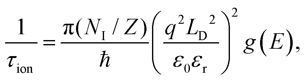 | (1) |
 | (2) |
Finally, electronic transport calculation was performed in PERTURBO based on the semi-classical Boltzmann transport method with energy-dependent total relaxation times. For comparison, the transport properties were also evaluated using BoltzTraP package48 with constant relaxation time approximation (CRTA).49 The transport calculations were performed in the in-plane directions and so, van der Waals interactions were not considered in the DFT and DFPT calculations. Using a similar approach, recently we have reproduced the thermoelectric transport properties of MoSe250 and SnSe2.51
In the case of phonons, we performed first-principles calculations by using the Vienna ab initio simulation (VASP),52–55 SCAN-rVV10 XC potential to calculate the harmonic and anharmonic interatomic force constants using a 4 × 4 × 2 supercell. The thermal conductivity of naturally occurring isotopic and hypothetical isotopically pure MoTe2 bulk was then calculated on a converged q-space grid 16 × 16 × 4 by iteratively solving the phonon Boltzmann transport equation as implemented in the Sheng-BTE package.56,57
Results and discussion
Electrical transport characterization
The electrical conductivity of the thin MoTe2 sample is plotted in Fig. 1(a) as a function of Vg. Without the application of the back gate voltage, the value was around 1350 S m−1. The conductivity of MoTe2 reported in the literature varies depending on the sample preparation. The observed electrical conductivity is within the reported literature values.30,31 In comparison to the samples from the two references, the electrical conductivity of our sample doubles that of the bulk MoTe2 crystal30 while it is one order of magnitude smaller than that of the sputtered thin film sample.31 As Vg is swept from −80 V to 80 V, its electrical conductivity varies by one order of magnitude, from 250 S m−1 to 2550 S m−1. The conductivity goes up with increasing gate voltages. Since Vg is connected to the highly doped Si, increasing Vg means increasing electron density in the sample and thus the sample exhibits n-type behavior. Another thicker sample of 100 nm was also measured and exhibited similar conductivity values and similar trends as a function of Vg. The results were included in ESI.† The Seebeck coefficient was measured at different Vg as shown in Fig. 1(b). The negative S value confirms the n-type conduction of the sample. At Vg = 0 V, the sample shows a Seebeck coefficient of −210 μV K−1. This room temperature value is about half of that of the bulk single crystal30 but one order of magnitude larger than that of the sputtered thin film.31 The Seebeck voltage detection was noisy in the entire measurement range which prevented reliable measurements at negative Vg. Moreover, at large negative Vg values, an offset open voltage was detected even when the heater was turned off, which should have been close to zero. Similar behavior has been observed and explained for MoS2: when the semiconductor channel resistance becomes too high, resistive coupling from the back gate to the channel causes the offset voltage.15 The input bias current up to 120 pA from the nanovoltmeter also contributes to the offset voltage and the noise, which was observed for MoS215 and for Si metal-oxide-semiconductor FETs with high resistance.58 Further complex annealing processing can potentially increase the number of vacancies accompanied by a decrease in resistivity and better resolution in Seebeck measurements.59 Presumably due to the noisy signals, no significant change in the Seebeck coefficient was observed within the Vg = 0–50 V range, although one could expect a lower Seebeck coefficient with higher electrical conductivity. The expected change in S value against Vg was calculated theoretically in the following section and is shown to be within our experimental error bars. The theoretical Seebeck coefficient reduces to −185 μV K−1 at Vg = 80 V and grows to −285 μV K−1 at Vg = −80 V (Fig. 1(b)).Electronic transport calculations
Since the devices are over 10 layers thick, they are considered bulk in the band structure calculations. Electronic band structure, electronic density of states (DOS), and phonon-dispersion of bulk MoTe2 are shown in Fig. 2. The obtained DFT band structure is in good agreement with previous calculations60,61 and Wannier interpolated band structure. The top of the valence band is at Γ, and the bottom of the conduction band is halfway between Γ–K, resulting in an indirect gap of 0.66 eV. It is well known that PBE functionals underestimate the bandgap for most insulators and semiconductors. So, we shifted the conduction bands during Wannier to PERTURBO interpolation and obtained a band gap of 0.87 eV which closely matches the experimental gap of 0.83 eV.26,27,62 | ||
| Fig. 2 (a) Electronic band structure, (b) electronic DOS from DFT, and (c) phonon dispersion of bulk MoTe2. | ||
The phonon dispersion of MoTe2 is shown along in-plane (Γ(0,0,0) → M(0.5,0.5,0.5) → K(0.333,0.333,0.000) → Γ(0,0,0)) and cross plane (Γ(0,0,0) → A(0,0,0.5)) direction in Fig. 2(c). As the unit cell of hexagonal MoTe2 has 6 atoms, there are 18 phonon modes at each k-point. Our results are in agreement with other DFPT calculations.63 The lowest three modes with linear dispersion around Γ point are the acoustic modes and the rest of the modes are the optical modes with higher vibrational frequencies. The optical phonon modes above 3 THz are relatively flat and do not contribute significantly to the phonon group velocity. The low-frequency optical modes (<3 THz) and acoustic modes are more dispersive and are important in controlling thermal transport in MoTe2. Besides, phonon group velocity towards in-plane is greater than that toward cross-plane direction yielding higher thermal conductivity along in-plane direction which is common for layered structured materials because of weak van der Waals interactions.64
The Seebeck coefficient and electrical conductivity at room temperature are evaluated using semi-classical BTE including electron–phonon scattering and ionized impurity scattering in the PERTRUBO package. The ionized impurity scattering rates are calculated using a modified Brooks-Herring approach and later, electron–phonon scattering is added using the Matthiessen rule. Both scattering rates are shown in Fig. 3 along with the electronic DOS. The total scattering times are dominated by the ionized impurity scattering because of the high impurity carrier concentration (2.9 × 1019 cm−3). Finally, Boltzmann transport calculations are performed considering energy-dependent total scattering times. At first, we used carrier concentration as a fitting parameter to match the experimental electrical conductivities at different gate voltages and reported the corresponding Seebeck coefficients. We found that the obtained Seebeck coefficients are within the error bar of the experimentally reported values in Fig. 1(b). Fig. 1(c) and (d) shows the raw theoretical calculations with no fitting of conductivity and Seebeck coefficient as a function of chemical potential and carrier concentration (1 × 1019 cm−3 to 4 × 1019 cm−3), respectively. At zero gate voltage, experimental electrical conductivity and Seebeck are around 1350 S m−1 and −210 μV K−1, respectively, which correspond to the carrier concentration of 2.9 × 1019 cm−3 and chemical potential of 0.6 eV above the intrinsic Fermi level (EF) as shown in Fig. 1(c) and (d). Carrier concentration increases with increasing gate voltages and therefore, electrical conductivity increases from 260 S m−1 to 2580 S m−1 whereas the Seebeck coefficient decreases from −300 μV K−1 to −189 μV K−1. Overall, the experimental values are within the range of predicted theoretical values.
 | ||
| Fig. 3 Scattering rates and DOS as a function of the energy relative to the conduction band minimum (EC). | ||
We have also analyzed the effects of electron–phonon and ionized impurity scattering on transport properties in MoTe2. With only electron–phonon scattering at zero bias, the BTE equation yields a Seebeck coefficient of −216 μV K−1 and electrical conductivity of 54096 S m−1. The inclusion of ionized impurity scattering does not change the Seebeck coefficient significantly and the value reduces slightly from −216 μV K−1 to −207 μV K−1 because the Seebeck coefficient is not sensitive to the details of relaxation times as shown in other first principles-based calculations.42,51 However, the electrical conductivity changes significantly with ionized impurity scattering and the final results are close to the experimental results. After successfully modeling the experimental Seebeck coefficient and electrical conductivity within energy-dependent relaxation time, we compared the results obtained from energy-dependent relaxation time and CRTA49 as shown in Table 1. The details of the Seebeck coefficient and electrical conductivity obtained from BoltzTraP48 are discussed in ESI† Fig. S2. Within CRTA, relaxation times are assumed to be energy and momentum-independent and the same constant for all electrons. As implemented in BoltzTraP, the constant relaxation time is not calculated. Hence, we take the average electron–phonon and ionized impurity scattering rates weighted by df/dE calculated within the Fermi-window (μ ± 20KBT) as the constant and use it in the CRTA calculations. This relaxation time at room temperature and at zero gate is 0.94 fs. Using this value, the obtained electrical conductivity is 2018 S m−1 and the Seebeck coefficient is −255 μV K−1. The discrepancies in the results between PERTURBO and BoltzTraP come from the use of different relaxation times.42,51,65 To accurately describe the transport properties of a material, energy or momentum-dependent scattering times need to be considered.
| Parameters | S (μV K−1) | σ (S m−1) | |
|---|---|---|---|
| Experiment | −210 | 1350 | |
| BoltzTrap-CRTA | −255 | 2018 | |
| PERTURBO | τ e–ph | −216 | 54096 |
| (τe–ph−1 + τion−1)−1 | −207 | 1400 | |
In-plane thermal transport
Heat diffusion imaging is used to measure the in-plane thermal conductivity of two flakes. The first one is the same 25 nm thickness as was used and annealed for the electrical measurements. An optical image of the sample as well as a thermoreflectance map is provided in Fig. 4(a) and (b). The sample surface temperature drops exponentially as a function of the distance away from the heater and can be fitted into a model for thermal conductivity extraction. Several example temperature decay curves along with an exponential fit are shown in Fig. 4(c). An in-plane thermal conductivity of 9.8 ± 3.7 W m−1 K−1 was obtained for MoTe2 at room temperature. The error accounts for the variations from the multiple extracted temperature decay profiles for averaging. The second flake is a 90 nm thick flake that is not annealed for which we extended our measurements down to 190 K. Fig. 5 summarises our measurements for these two flakes as well as data from the literature for bulk,66 supported, and unsupported flakes.67 The thermal conductivity measurement versus thickness follows an expected trend where the thermal conductivity is reduced for thinner samples. | ||
| Fig. 4 (a) Optical image of the MoTe2 device for thermal transport measurement. The scale bar is 5 μm. (b) Thermoreflectance map of the sample surface with 5 V supplied to the heater. Temperature decay curves were taken along the sample perpendicular to the heater. (c) Temperature decay curves and their corresponding exponential fit for thermal conductivity extraction. | ||
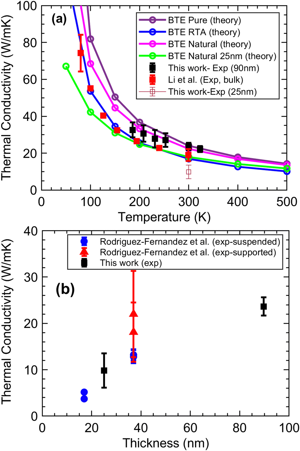 | ||
| Fig. 5 (a) Calculated thermal conductivity versus temperature of natural and pure MoTe2 bulk along the in-plane direction using iterative solutions of BTE. The green line represents the theoretical thermal conductivity when boundary scattering (25 nm size) is included and results for RTA solutions of BTE (bulk-non-iterative) are plotted in blue for comparison. Experimental in-plane thermal conductivity of 90 nm (not annealed) and 25 nm (annealed) thick flakes and literature data of bulk 2H-MoTe266 are shown with squares. (b) Experimental in-plane thermal conductivity of 2H-MoTe2 as a function of thickness at room temperature, compared with flakes measured by opto-thermal Raman technique.67 | ||
According to the Wiedemann–Franz law,68 the electronic contribution to the thermal conductivity is only on the order of 0.01 W m−1 K−1, which is negligible even with back gate modulation added. Therefore, we assume gating does not change the thermal conductivity. For the same reason, in our theoretical approach, we only include lattice thermal conductivity calculations using first principles as discussed in the methods. Fig. 5(a) shows the temperature dependence of the calculated thermal conductivity of MoTe2 bulk along the in-plane direction versus temperature. The lattice thermal conductivity of MoTe2 is calculated within both the relaxation time approximation (RTA) considering 3-phonon processes and the full iterative solution to the phonon Boltzmann equation for an isotopically pure sample. While the RTA results are closer to the experimentally measured bulk values, it is known that the RTA solution gives a poor approximation to the lattice thermal conductivity compared to the full iterative method. These results are obtained by considering the interaction cutoff for cubic interatomic force constants calculations up to the seventh nearest neighbor. At room temperature, the calculated thermal conductivity of the isotopically pure bulk MoTe2 is 24 W m−1 K−1. The addition of the naturally occurring isotope scattering lowers the thermal conductivity by 10% to 22 W m−1 K−1. This value is close to ∼19 W m−1 K−1 reported for bulk MoTe266 and 23.6 ± 1.96 W m−1 K−1 measured for our 90 nm thick flake.
The value measured for our 25 nm thick sample is much smaller and is 9.8 ± 3.7 W m−1 K−1 which as shown in Fig. 5(b) is consistent with other literature data reported but it is not consistent with the theoretical calculations. Part of the difference is from the boundary scattering. The addition of the size effect in the simplest approximation can be done by adding a v/L term, where v is the group velocity and L is the thickness, to the scattering rates to serve as the boundary scattering. The addition of this boundary scattering term lowers the theoretical thermal conductivity further by 22% and is shown in the plot by the green dashed line. This is still larger than the experimentally measured value for the thin 25 nm flake. The difference can be attributed to defects (Te vacancies) inside the experimental sample as well as phonon–electron scattering rates. We note that our thin flake was annealed and hence contains more Te vacancies which are beneficial in increasing the electrical conductivity as was discussed.
Power factor and ZT
The peak power factor of thin MoTe2 is expected to occur at the highest positive gate voltage since the improvement from the increasing electrical conductivity exceeds the impact from the decreasing Seebeck coefficient. By combining the experimental electrical conductivity and the theoretically predicted Seebeck coefficient, the peak PFT reaches 0.027 W m−1 K−1 at Vg = 80 V. Although our sample does not possess the highest electrical conductivity or the largest Seebeck coefficient value in comparison to the other two literature samples, by reaching a good balance between the two interrelated parameters, our peak PFT is comparable to the bulk single crystal MoTe2 value30 and is one order of magnitude larger than that of sputtered thin film MoTe2.31 Compared to the value of 0.018 W m−1 K−1 at Vg = 0 V, the back gate modulation is able to enhance the PFT by 45%.The peak ZT at room temperature is about 0.003. We expect the figure of merit to improve at higher temperatures, as was seen in the case of MoTe2 thin films wherein the pick power factor was observed at 450 K for p-type, the sample then changed to n-type at around 560 K and the power factor continued increasing until 670 K.31 However, we also note that MoTe2 becomes less stable as the temperature rises. It has been observed that Te vacancies start to form at above 473 K. It is shown that surface and edge passivation can enhance the stability of MoTe2 up to 773 K.47 Its performance might be further improved via a few routes. For example, previous research has shown that hBN substrate is flatter and has fewer charge puddles compared to SiO2, which can greatly improve the transport properties of 2D samples.6,13 Estimation based on experimental conductivity and carrier concentration indicates that the mobility of the sample was only 3 cm2 V−1 s−1. Optimization of the fabrication process might produce samples with higher mobility.
Conclusions
In summary, we have exfoliated and fabricated 2H-MoTe2 samples from single crystal flakes for in-plane thermoelectric transport characterization. Back gate bias was applied to adjust the Fermi level of the device and thus the electrical properties. The electrical conductivity increased with increasing gate voltages while the Seebeck coefficient values remained constant within the experimental error bar. The peak PFT of 0.027 W m−1 K−1 was obtained at the largest positive bias of +80 V, which was a 45% increase compared to the zero-bias value. These experimental results were in agreement with first-principles calculations which accounted for electron–phonon scattering and ionized impurity scattering. It was shown that at room temperatures, the ionized impurity scattering rate is the dominant one in the studied sample with values exceeding electron–phonon scattering rates by two orders of magnitude. The in-plane thermal conductivity is measured using heat diffusion imaging and is 9.8 ± 3.7 W m−1 K−1 for the 25 nm thick flake and 23.6 ± 1.96 W m−1 K−1 for the 90 nm thick sample at room temperature. The values are consistent with reported values in the literature. However, the value of the 25 nm sample is consistently lower than the calculated results using the first-principles approach as the latter does not include phonon scattering due to defects (Te vacancies) and electrons. The power factor and the ZT values will be larger at higher temperatures as previously shown in the literature. The thermal conductivity can be manipulated and increased by 3.9 W m−1 K−1 under a 1 K temperature difference, by applying an optimum electrical current for active cooling applications. Further enhancement of the device performance might be achieved by increasing the temperature, using hBN as a substrate, and optimizing fabrication processes to increase carrier mobility. This study adds to the 2D thermoelectric database and is a solid first step in utilizing 2D 2H-MoTe2 as a thermoelectric material.Disclaimer
Certain commercial equipment, instruments, or materials, commercial or non-commercial, are identified in this paper in order to specify the experimental procedure adequately. Such identification is not intended to imply recommendation or endorsement by the National Institute of Standards and Technology, nor is it intended to imply that the materials or equipment identified are necessarily the best available for the purpose.Author contributions
M. Z. supervised the project. T. Z. fabricated the devices and performed experimental characterizations. S. S. D. performed the electronic first-principles calculations. S. N. and K. E. performed the thermal conductivity calculations. F. F. T performed low-temperature thermal conductivity measurements. S. K. and A. V. D. grew MoTe2 single crystals. C. C. helped with AFM measurements. T. Z., S. S. D., and M. Z. drafted the manuscript. All authors reviewed the manuscript prior to submission.Conflicts of interest
There are no conflicts to declare.Acknowledgements
T. Z., S. S. D., and M. Z. acknowledge the support by NSF, grant number 2230352. S. K. and A. V. D. acknowledge support through the Materials Genome Initiative funding allocated to the National Institute of Standards and Technology. K. E. and S. N. acknowledge the support by NSF-CSSI, grant number 2103989.Notes and references
- Q. Li, Q. Hao, T. Zhu, M. Zebarjadi and K. Takahashi, Nanostructured and Heterostructured 2D Materials for Thermoelectrics, Eng. Sci., 2021, 13, 24–50, DOI:10.30919/es8d1136.
- E. Pop, Energy Dissipation and Transport in Nanoscale Devices, Nano Res., 2010, 3(3), 147–169, DOI:10.1007/s12274-010-1019-z.
- D. Akinwande, C. J. Brennan, J. S. Bunch, P. Egberts, J. R. Felts, H. Gao, R. Huang, J.-S. Kim, T. Li, Y. Li, K. M. Liechti, N. Lu, H. S. Park, E. J. Reed, P. Wang, B. I. Yakobson, T. Zhang, Y.-W. Zhang, Y. Zhou and Y. Zhu, A Review on Mechanics and Mechanical Properties of 2D Materials—Graphene and Beyond, Extrem. Mech. Lett., 2017, 13, 42–77, DOI:10.1016/j.eml.2017.01.008.
- P. Ares and K. S. Novoselov, Recent Advances in Graphene and Other 2D Materials, Nano Mater. Sci., 2022, 4(1), 3–9, DOI:10.1016/J.NANOMS.2021.05.002.
- K. S. Novoselov, A. K. Geim, S. V. Morozov, D. Jiang, Y. Zhang, S. V. Dubonos, I. V. Grigorieva and A. A. Firsov, Electric Field Effect in Atomically Thin Carbon Films, Science, 2004, 306(5696), 666–669, DOI:10.1126/science.1102896.
- J. Duan, X. Wang, X. Lai, G. Li, K. Watanabe, T. Taniguchi, M. Zebarjadi and E. Y. Andrei, High Thermoelectricpower Factor in Graphene/HBN Devices, Proc. Natl. Acad. Sci. U. S. A., 2016, 113(50), 14272–14276, DOI:10.1073/pnas.1615913113.
- M. Zebarjadi, Electronic Cooling Using Thermoelectric Devices, Appl. Phys. Lett., 2015, 106(20), 203506, DOI:10.1063/1.4921457.
- M. J. Adams, M. Verosky, M. Zebarjadi and J. P. Heremans, High Switching Ratio Variable-Temperature Solid-State Thermal Switch Based on Thermoelectric Effects, Int. J. Heat Mass Transf., 2019, 134, 114–118, DOI:10.1016/J.IJHEATMASSTRANSFER.2018.12.154.
- M. J. Adams, M. Verosky, M. Zebarjadi and J. P. Heremans, Active Peltier Coolers Based on Correlated and Magnon-Drag Metals, Phys. Rev. Appl., 2019, 11(5), 054008, DOI:10.1103/PhysRevApplied.11.054008.
- G. J. Snyder and E. S. Toberer, Complex Thermoelectric Materials, Nat. Mater., 2008, 7(2), 105–114, DOI:10.1038/nmat2090.
- M. Markov, X. Hu, H.-C. Liu, N. Liu, S. J. Poon, K. Esfarjani and M. Zebarjadi, Semi-Metals as Potential Thermoelectric Materials, Sci. Rep., 2018, 8(1), 9876, DOI:10.1038/s41598-018-28043-3.
- K. Hippalgaonkar, Y. Wang, Y. Ye, D. Y. Qiu, H. Zhu, Y. Wang, J. Moore, S. G. Louie and X. Zhang, High Thermoelectric Power Factor in Two-Dimensional Crystals of MoS2, Phys. Rev. B, 2017, 95(11), 115407, DOI:10.1103/PhysRevB.95.115407.
- J. Wu, Y. Liu, Y. Liu, Y. Cai, Y. Zhao, H. K. Ng, K. Watanabe, T. Taniguchi, G. Zhang, C.-W. Qiu, D. Chi, A. H. C. Neto, J. T. L. Thong, K. P. Loh and K. Hippalgaonkar, Large Enhancement of Thermoelectric Performance in MoS2/h-BN Heterostructure Due to Vacancy-Induced Band Hybridization, Proc. Natl. Acad. Sci. U. S. A., 2020, 117(25), 13929–13936, DOI:10.1073/pnas.2007495117.
- J. Wu, H. Schmidt, K. K. Amara, X. Xu, G. Eda and B. Özyilmaz, Large Thermoelectricity via Variable Range Hopping in Chemical Vapor Deposition Grown Single-Layer MoS2, Nano Lett., 2014, 14(5), 2730–2734, DOI:10.1021/nl500666m.
- M. Kayyalha, J. Maassen, M. Lundstrom, L. Shi and Y. P. Chen, Gate-Tunable and Thickness-Dependent Electronic and Thermoelectric Transport in Few-Layer MoS2, J. Appl. Phys., 2016, 120(13), 134305, DOI:10.1063/1.4963364.
- R. Yan, J. R. Simpson, S. Bertolazzi, J. Brivio, M. Watson, X. Wu, A. Kis, T. Luo, A. R. Hight Walker and H. G. Xing, Thermal Conductivity of Monolayer Molybdenum Disulfide Obtained from Temperature-Dependent Raman Spectroscopy, ACS Nano, 2014, 8(1), 986–993, DOI:10.1021/nn405826k.
- X. Zhang, D. Sun, Y. Li, G.-H. Lee, X. Cui, D. Chenet, Y. You, T. F. Heinz and J. C. Hone, Measurement of Lateral and Interfacial Thermal Conductivity of Single- and Bilayer MoS2 and MoSe2 Using Refined Optothermal Raman Technique, ACS Appl. Mater. Interfaces, 2015, 7(46), 25923–25929, DOI:10.1021/acsami.5b08580.
- M. Rahman, M. Shahzadeh and S. Pisana, Simultaneous Measurement of Anisotropic Thermal Conductivity and Thermal Boundary Conductance of 2-Dimensional Materials, J. Appl. Phys., 2019, 126(20), 205103, DOI:10.1063/1.5118315.
- M. Yarali, X. Wu, T. Gupta, D. Ghoshal, L. Xie, Z. Zhu, H. Brahmi, J. Bao, S. Chen, T. Luo, N. Koratkar and A. Mavrokefalos, Effects of Defects on the Temperature-Dependent Thermal Conductivity of Suspended Monolayer Molybdenum Disulfide Grown by Chemical Vapor Deposition, Adv. Funct. Mater., 2017, 27(46), 1704357, DOI:10.1002/adfm.201704357.
- I. Jo, M. T. Pettes, E. Ou, W. Wu and L. Shi, Basal-Plane Thermal Conductivity of Few-Layer Molybdenum Disulfide, Appl. Phys. Lett., 2014, 104(20), 201902, DOI:10.1063/1.4876965.
- Y. Zhao, M. Zheng, J. Wu, B. Huang and J. T. L. Thong, Studying Thermal Transport in Suspended Monolayer Molybdenum Disulfide Prepared by a Nano-Manipulator-Assisted Transfer Method, Nanotechnology, 2020, 31(22), 225702, DOI:10.1088/1361-6528/ab7647.
- A. J. Gabourie, S. V. Suryavanshi, A. B. Farimani and E. Pop, Reduced Thermal Conductivity of Supported and Encased Monolayer and Bilayer MoS2, 2D Mater., 2021, 8(1), 011001, DOI:10.1088/2053-1583/aba4ed.
- C. Ruppert, B. Aslan and T. F. Heinz, Optical Properties and Band Gap of Single- and Few-Layer MoTe2 Crystals, Nano Lett., 2014, 14(11), 6231–6236, DOI:10.1021/nl502557g.
- I. G. Lezama, A. Arora, A. Ubaldini, C. Barreteau, E. Giannini, M. Potemski and A. F. Morpurgo, Indirect-to-Direct Band Gap Crossover in Few-Layer MoTe2, Nano Lett., 2015, 15(4), 2336–2342, DOI:10.1021/nl5045007.
- Y. Yang, X. Zhu, K. Zhang, H. Zhu, L. Chen and Q. Sun, Observation of Different Transport Behaviors in a Two-Dimensional MoTe2 Field-Effect Transistor with Engineered Gate Stack, Microelectron. Eng., 2021, 237, 111497, DOI:10.1016/j.mee.2020.111497.
- C. Gong, Y. Zhang, W. Chen, J. Chu, T. Lei, J. Pu, L. Dai, C. Wu, Y. Cheng, T. Zhai, L. Li and J. Xiong, Electronic and Optoelectronic Applications Based on 2D Novel Anisotropic Transition Metal Dichalcogenides, Adv. Sci., 2017, 4(12), 1700231, DOI:10.1002/advs.201700231.
- Y.-F. Lin, Y. Xu, S.-T. Wang, S.-L. Li, M. Yamamoto, A. Aparecido-Ferreira, W. Li, H. Sun, S. Nakaharai, W.-B. Jian, K. Ueno and K. Tsukagoshi, Ambipolar MoTe2 Transistors and Their Applications in Logic Circuits, Adv. Mater., 2014, 26(20), 3263–3269, DOI:10.1002/adma.201305845.
- Y.-M. Chang, C.-Y. Lin, Y.-F. Lin and K. Tsukagoshi, Two-Dimensional MoTe2 Materials: From Synthesis, Identification, and Charge Transport to Electronics Applications, Jpn. J. Appl. Phys., 2016, 55(11), 1102A1, DOI:10.7567/JJAP.55.1102A1.
- Y.-Q. Bie, G. Grosso, M. Heuck, M. M. Furchi, Y. Cao, J. Zheng, D. Bunandar, E. Navarro-Moratalla, L. Zhou, D. K. Efetov, T. Taniguchi, K. Watanabe, J. Kong, D. Englund and P. Jarillo-Herrero, A MoTe2-Based Light-Emitting Diode and Photodetector for Silicon Photonic Integrated Circuits, Nat. Nanotechnol., 2017, 12(12), 1124–1129, DOI:10.1038/nnano.2017.209.
- A. Conan, D. Delaunay, A. Bonnet, A. G. Moustafa and M. Spiesser, Temperature Dependence of the Electrical Conductivity and Thermoelectric Power in MoTe2 Single Crystals, Phys. Status Solidi, 1979, 94(1), 279–286, DOI:10.1002/pssb.2220940132.
- D. Shi, G. Wang, C. Li, X. Shen and Q. Nie, Preparation and Thermoelectric Properties of MoTe2 Thin Films by Magnetron Co-Sputtering, Vacuum, 2017, 138, 101–104, DOI:10.1016/j.vacuum.2017.01.030.
- X.-J. Yan, Y.-Y. Lv, L. Li, X. Li, S.-H. Yao, Y.-B. Chen, X.-P. Liu, H. Lu, M.-H. Lu and Y.-F. Chen, Investigation on the Phase-Transition-Induced Hysteresis in the Thermal Transport along the c-Axis of MoTe2, npj Quantum Mater., 2017, 2(1), 31, DOI:10.1038/s41535-017-0031-x.
- A. Shafique and Y. H. Shin, Strain Engineering of Phonon Thermal Transport Properties in Monolayer 2H-MoTe2, Phys. Chem. Chem. Phys., 2017, 19(47), 32072–32078, 10.1039/C7CP06065C.
- R. Addou, C. M. Smyth, J.-Y. Noh, Y.-C. Lin, Y. Pan, S. M. Eichfeld, S. Fölsch, J. A. Robinson, K. Cho, R. M. Feenstra and R. M. Wallace, One Dimensional Metallic Edges in Atomically Thin WSe 2 Induced by Air Exposure, 2D Mater., 2018, 5(2), 025017, DOI:10.1088/2053-1583/aab0cd.
- T. Zhu, D. H. Olson, P. E. Hopkins and M. Zebarjadi, Heat Diffusion Imaging: In-Plane Thermal Conductivity Measurement of Thin Films in a Broad Temperature Range, Rev. Sci. Instrum., 2020, 91(11), 113701, DOI:10.1063/5.0024476.
- W. Jang, Z. Chen, W. Bao, C. N. Lau and C. Dames, Thickness-Dependent Thermal Conductivity of Encased Graphene and Ultrathin Graphite, Nano Lett., 2010, 10(10), 3909–3913, DOI:10.1021/nl101613u.
- T. Zhu, P. M. Litwin, M. G. Rosul, D. Jessup, M. S. Akhanda, F. F. Tonni, S. Krylyuk, A. V. Davydov, P. Reinke, S. J. McDonnell and M. Zebarjadi, Transport Properties of Few-Layer NbSe2: From Electronic Structure to Thermoelectric Properties, Mater. Today Phys., 2022, 27, 100789, DOI:10.1016/j.mtphys.2022.100789.
- P. Giannozzi, S. Baroni, N. Bonini, M. Calandra, R. Car, C. Cavazzoni, D. Ceresoli, G. L. Chiarotti, M. Cococcioni, I. Dabo, A. Dal Corso, S. de Gironcoli, S. Fabris, G. Fratesi, R. Gebauer, U. Gerstmann, C. Gougoussis, A. Kokalj, M. Lazzeri, L. Martin-Samos, N. Marzari, F. Mauri, R. Mazzarello, S. Paolini, A. Pasquarello, L. Paulatto, C. Sbraccia, S. Scandolo, G. Sclauzero, A. P. Seitsonen, A. Smogunov, P. Umari and R. M. Wentzcovitch, QUANTUM ESPRESSO: A Modular and Open-Source Software Project for Quantum Simulations of Materials, J. Phys.: Condens. Matter, 2009, 21(39), 395502, DOI:10.1088/0953-8984/21/39/395502.
- D. Vanderbilt, Soft Self-Consistent Pseudopotentials in a Generalized Eigenvalue Formalism, Phys. Rev. B: Condens. Matter Mater. Phys., 1990, 41(11), 7892–7895, DOI:10.1103/PhysRevB.41.7892.
- J. P. Perdew, A. Ruzsinszky, G. I. Csonka, O. A. Vydrov, G. E. Scuseria, L. A. Constantin, X. Zhou and K. Burke, Restoring the Density-Gradient Expansion for Exchange in Solids and Surfaces, Phys. Rev. Lett., 2008, 100(13), 136406, DOI:10.1103/PhysRevLett.100.136406.
- J. A. Wilson and A. D. Yoffe, The Transition Metal Dichalcogenides Discussion and Interpretation of the Observed Optical, Electrical and Structural Properties, Adv. Phys., 1969, 18(73), 193–335, DOI:10.1080/00018736900101307.
- J.-J. Zhou, J. Park, I.-T. Lu, I. Maliyov, X. Tong and M. Bernardi, Perturbo: A Software Package for Ab Initio Electron–Phonon Interactions, Charge Transport and Ultrafast Dynamics, Comput. Phys. Commun., 2021, 264, 107970, DOI:10.1016/j.cpc.2021.107970.
- M. Lundstrom, Fundamentals of Carrier Transport, 2nd Edn, Meas. Sci. Technol., 2002, 13(2), 230, DOI:10.1088/0957-0233/13/2/703.
- N. Marzari, A. A. Mostofi, J. R. Yates, I. Souza and D. Vanderbilt, Maximally Localized Wannier Functions: Theory and Applications, Rev. Mod. Phys., 2012, 84(4), 1419–1475, DOI:10.1103/RevModPhys.84.1419.
- F. Giustino, M. L. Cohen and S. G. Louie, Electron-Phonon Interaction Using Wannier Functions, Phys. Rev. B: Condens. Matter Mater. Phys., 2007, 76(16), 165108 CrossRef.
- J. Liu, Y. Wang, X. Xiao, K. Zhang, N. Guo, Y. Jia, S. Zhou, Y. Wu, Q. Li and L. Xiao, Conversion of Multi-Layered MoTe2 Transistor Between P-Type and N-Type and Their Use in Inverter, Nanoscale Res. Lett., 2018, 13(1), 291, DOI:10.1186/s11671-018-2721-0.
- H. Zhu, Q. Wang, L. Cheng, R. Addou, J. Kim, M. J. Kim and R. M. Wallace, Defects and Surface Structural Stability of MoTe2 under Vacuum Annealing, ACS Nano, 2017, 11(11), 11005–11014, DOI:10.1021/acsnano.7b04984.
- G. K. H. Madsen and D. J. Singh, BoltzTraP. A Code for Calculating Band-Structure Dependent Quantities, Comput. Phys. Commun., 2006, 175(1), 67–71, DOI:10.1016/j.cpc.2006.03.007.
- B. R. Nag, Electron Transport in Compound Semiconductors, ed. B. Nag, Springer Series in Solid-State Sciences, Springer Berlin Heidelberg, Berlin, Heidelberg, 1980, vol. 11 DOI:10.1007/978-3-642-81416-7.
- M. G. Rosul and M. Zebarjadi, Effect of Electron-Phonon Interaction and Ionized Impurity Scattering on the Room-Temperature Thermoelectric Properties of Bulk MoSe2, J. Phys. Chem. C, 2022, 126(35), 15011–15018, DOI:10.1021/acs.jpcc.2c03782.
- S. Das, G. Rosul and M. Zebarjadi, Optimization of the Thermoelectric Properties of SnSe2 Using First-Principles Calculations, J. Phys. Chem. C, 2023, 127(14), 6916–6924, DOI:10.1021/acs.jpcc.2c09137.
- G. Kresse and J. Hafner, Ab Initio Molecular-Dynamics Simulation of the Liquid-Metal–Amorphous-Semiconductor Transition in Germanium, Phys. Rev. B: Condens. Matter Mater. Phys., 1994, 49(20), 14251–14269, DOI:10.1103/PhysRevB.49.14251.
- G. Kresse and J. Furthmüller, Efficiency of Ab-Initio Total Energy Calculations for Metals and Semiconductors Using a Plane-Wave Basis Set, Comput. Mater. Sci., 1996, 6(1), 15–50, DOI:10.1016/0927-0256(96)00008-0.
- G. Kresse and J. Furthmüller, Efficient Iterative Schemes for Ab Initio Total-Energy Calculations Using a Plane-Wave Basis Set, Phys. Rev. B: Condens. Matter Mater. Phys., 1996, 54(16), 11169–11186, DOI:10.1103/PhysRevB.54.11169.
- G. Kresse and D. Joubert, From Ultrasoft Pseudopotentials to the Projector Augmented-Wave Method, Phys. Rev. B: Condens. Matter Mater. Phys., 1999, 59(3), 1758–1775, DOI:10.1103/PhysRevB.59.1758.
- W. Li, L. Lindsay, D. A. Broido, D. A. Stewart and N. Mingo, Thermal Conductivity of Bulk and Nanowire Mg2SixSn1−x Alloys from First Principles, Phys. Rev. B: Condens. Matter Mater. Phys., 2012, 86(17), 174307, DOI:10.1103/PhysRevB.86.174307.
- W. Li, J. Carrete, A. Katcho and N. Mingo, ShengBTE: A Solver of the Boltzmann Transport Equation for Phonons, Comput. Phys. Commun., 2014, 185(6), 1747–1758, DOI:10.1016/j.cpc.2014.02.015.
- R. Fletcher, V. M. Pudalov, A. D. B. Radcliffe and C. Possanzini, Critical Behaviour of Thermopower and Conductivity at the Metal-Insulator Transition in High-Mobility Si-MOSFETs, Semicond. Sci. Technol., 2001, 16(5), 386–393, DOI:10.1088/0268-1242/16/5/318.
- M. J. Kim, W. Y. Lee, M. S. Kang, S. H. Kim, J. M. Cho, Y. H. Kim, J. W. Choi, N. W. Park, G. S. Kim, Y. G. Yoon and S. K. Lee, Intrinsic Seebeck Coefficients of 2D Polycrystalline PtSe2 Semiconducting Films through Two-Step Annealing, J. Mater. Chem. A, 2023, 11(11), 5714–5724, 10.1039/D2TA10079G.
- W. S. Yun, S. W. Han, S. C. Hong, I. G. Kim and J. D. Lee, Thickness and Strain Effects on Electronic Structures of Transition Metal Dichalcogenides: 2H-MX2 Semiconductors (M = Mo, W;X = S, Se, Te), Phys. Rev. B: Condens. Matter Mater. Phys., 2012, 85(3), 033305, DOI:10.1103/PhysRevB.85.033305.
- A. H. Reshak and S. Auluck, Band Structure and Optical Response of 2H−MoX2compounds (X = S, Se, and Te), Phys. Rev. B: Condens. Matter Mater. Phys., 2005, 71(15), 155114, DOI:10.1103/PhysRevB.71.155114.
- G. Froehlicher, E. Lorchat and S. Berciaud, Direct versus Indirect Band Gap Emission and Exciton-Exciton Annihilation in Atomically Thin Molybdenum Ditelluride MoTe2, Phys. Rev. B, 2016, 94(8), 085429, DOI:10.1103/PhysRevB.94.085429.
- N. A. Pike, A. Dewandre, B. Van Troeye, X. Gonze and M. J. Verstraete, Vibrational and Dielectric Properties of the Bulk Transition Metal Dichalcogenides, Phys. Rev. Mater, 2018, 2(6), 063608, DOI:10.1103/PhysRevMaterials.2.063608.
- Z.-Y. Dong, Y. Zhou, X.-Q. Chen, W.-J. Li, Z.-Y. Cao, C. Luo, G.-H. Zhong, Q. Peng, X. Wu and X.-J. Chen, Effect of Low-Frequency Optical Phonons on the Thermal Conductivity of 2H Molybdenum Disulfide, Phys. Rev. B, 2022, 105(18), 184301, DOI:10.1103/PhysRevB.105.184301.
- G. Casu, A. Bosin and V. Fiorentini, Efficient Thermoelectricity in Sr2Nb2O7 with Energy-Dependent Relaxation Times, Phys. Rev. Mater., 2020, 4(7), 075404, DOI:10.1103/PhysRevMaterials.4.075404.
- H. Li, T. Pandey, Y. Jiang, X. Gu, L. Lindsay and Y. K. Koh, Origins of Heat Transport Anisotropy in MoTe2 and Other Bulk van der Waals Materials, Mater. Today Phys., 2023, 101196, DOI:10.1016/j.mtphys.2023.101196.
- C. Rodriguez-Fernandez, A. Nieminen, F. Ahmed, J. Pietila, H. Lipsanen and H. Caglayan, Unraveling Thermal Transport Properties of MoTe2 Thin Films Using the Optothermal Raman Technique, ACS Appl. Mater. Interfaces, 2023, 15(29), 35692–35700, DOI:10.1021/acsami.3c06134.
- C. Kittel, Introduction to Solid State Physics, 2005 Search PubMed.
Footnotes |
| † Electronic supplementary information (ESI) available. See DOI: https://doi.org/10.1039/d3ya00316g |
| ‡ Present address: Department of Physics, University of California, Santa Cruz, California, 95064, USA. |
| This journal is © The Royal Society of Chemistry 2023 |