
 Open Access Article
 This Open Access Article is licensed under a Creative Commons Attribution-Non Commercial 3.0 Unported Licence
Synthetic approaches for perovskite thin films and single-crystals
Anastasia
Soultati
 a,
Marinos
Tountas
b,
Konstantina K.
Armadorou
a,
Abd. Rashid bin Mohd
Yusoff
c,
Maria
Vasilopoulou
*a and
Mohammad Khaja
Nazeeruddin
*d
a,
Marinos
Tountas
b,
Konstantina K.
Armadorou
a,
Abd. Rashid bin Mohd
Yusoff
c,
Maria
Vasilopoulou
*a and
Mohammad Khaja
Nazeeruddin
*d
aInstitute of Nanoscience and Nanotechnology, National Centre for Scientific Research Demokritos, 15341 Agia Paraskevi, Attica, Greece. E-mail: m.vasilopoulou@inn.demokritos.gr
bDepartment of Electrical Engineering, Hellenic Mediterranean University, Estavromenos, 71410 Heraklion Crete, Greece
cDepartment of Chemical Engineering, Pohang University of Science and Technology (POSTECH), Pohang, Gyeongbuk 37673, Republic of Korea
dGroup for Molecular Engineering of Functional Materials, Institute of Chemical Sciences and Engineering, École Polytechnique Fédérale de Lausanne (EPFL), Rue de l’Industrie 17, CH-1951 Sion, Switzerland. E-mail: mdkhaja.nazeeruddin@epfl.ch
First published on 5th June 2023
Abstract
Halide perovskites are compelling candidates for the next generation of clean-energy-harvesting photovoltaic technologies owing to an unprecedented increase in power conversion efficiency and their low cost, facile fabrication and outstanding semiconductor properties. The potential of perovskite materials has been identified by understanding the fundamental science of perovskites such as crystallisation dynamics and charge carrier dynamics and finding various novel perovskite combinations from the periodic table. Current evidence suggests that the synthetic approach applied for the deposition of halide perovskite layers is a key factor dictating device efficiency and stability. In this review, we aim to investigate the large variety of synthetic procedures followed for the deposition of perovskite polycrystalline films and single crystal layers. We will summarize the current understanding and ability to influence material properties by using these synthetic methods and explore the link between synthetic approaches and material properties relevant to photovoltaic and other applications.
1. Introduction
Halide perovskites (HPs) have recently drawn great attention due to their outstanding optoelectronic properties, such as their solution processability,1–4 high absorption coefficients, ambipolar charge carrier mobility and large carrier diffusion lengths, and facilely tunable composition and dimensionality5–7 that can potentially enable the corresponding devices to exhibit unprecedented performances.8–14 This unique combination of properties has stimulated intense research studies in solar cells,15–20 light emitting diodes (LEDs),21–25 field effect transistors (FETs),26–29 and memories.30–33 The significant performance metrics that have been achieved in these optoelectronic devices are strongly dictated by the method these HPs are synthesized/deposited in thin films. Moreover, perovskite single-crystals have also emerged as an alternative material platform that can overcome the limitations of common polycrystalline films.34–38 For both perovskite films and single crystals, appropriate synthetic protocols are applied aiming to fabricate a high quality perovskite material and layer and the corresponding device that meets the specific needs of a given application.However, the soft lattice of these perovskites poses several challenges to the formation of smooth, pinhole-free perovskite films.39–49 Many methods have already been developed for the efficient synthesis and processing of polycrystalline films and single crystal layers. The aim of this review is to summarize recent approaches for the synthesis of perovskite films, both polycrystalline and single-crystal based, and discuss the advantages and obstacles encountered with each of these methods used to deposit this family of materials. This review is intended to be comprehensive and to provide a thorough description of the large variety of different processing routes applied for halide perovskite thin films and single crystals. A brief description of the basic halide perovskite material properties is given prior to the presentation of their fabrication methods, aiming to make the paper also accessible not only to those wishing to gain a holistic understanding of the whole field but also to those seeking essential information regarding a certain type of deposition process.
2. Structures, compositions and properties of 3D and 2D halide perovskites
Three-dimensional (3D) halide perovskites (HPs) crystallize in the ABX3 perovskite structure, where A and B are monovalent and divalent cations, respectively, and X is a halide anion. The A+ cations, in particular, are larger than the B2+ metallic ones and function as structural templates with their shape, size, and charge distribution being crucial factors for the stabilization of the perovskite structure. More specifically, A+ is usually an organic (CH3NH3+, methylammonium, MA; formamidinium, FA; CH6N3+, guanidinium, Gua) or inorganic (caesium, Cs+) cation, B2+ is a large atomic number metal (such as lead, Pb2+; tin, Sn2+ and germanium, Ge2+) and X− is a halogen (chloride, Cl−; bromide, Br−; and iodide, I−).The simplest possible ABX3 perovskite consists of a high-symmetry cubic structure belonging to the space group Pm![[3 with combining macron]](https://www.rsc.org/images/entities/char_0033_0304.gif) m.50 In this structure the halogen anions X− occupy the vertices in [BX6]4− octahedra, which share corners in all three orthogonal directions to generate infinite 3D [BX3]− frameworks, while the divalent metal cations B2+ are placed at the centers of these octahedra (Fig. 1).51 The smallest volume enclosed by neighbouring octahedra defines a cuboctahedral cavity and hosts the monovalent cation A+. Different possible perovskite structures can be regarded as being obtained by rotating or distorting the BX6 octahedra, displacing the B2+ metal cations off-center and rotating the A+ cations within the cuboctahedral cavity. More than one structure is usually found for a perovskite material with a given chemical composition, depending on the temperature and preparation method. For example, methylammonium lead triiodide (MAPbI3), a prototypical hybrid organic–inorganic metal halide perovskite, can undergo phase transformations from cubic to tetragonal at a temperature of 54 °C and from tetragonal to orthorhombic at −111 °C during cooling.52
m.50 In this structure the halogen anions X− occupy the vertices in [BX6]4− octahedra, which share corners in all three orthogonal directions to generate infinite 3D [BX3]− frameworks, while the divalent metal cations B2+ are placed at the centers of these octahedra (Fig. 1).51 The smallest volume enclosed by neighbouring octahedra defines a cuboctahedral cavity and hosts the monovalent cation A+. Different possible perovskite structures can be regarded as being obtained by rotating or distorting the BX6 octahedra, displacing the B2+ metal cations off-center and rotating the A+ cations within the cuboctahedral cavity. More than one structure is usually found for a perovskite material with a given chemical composition, depending on the temperature and preparation method. For example, methylammonium lead triiodide (MAPbI3), a prototypical hybrid organic–inorganic metal halide perovskite, can undergo phase transformations from cubic to tetragonal at a temperature of 54 °C and from tetragonal to orthorhombic at −111 °C during cooling.52
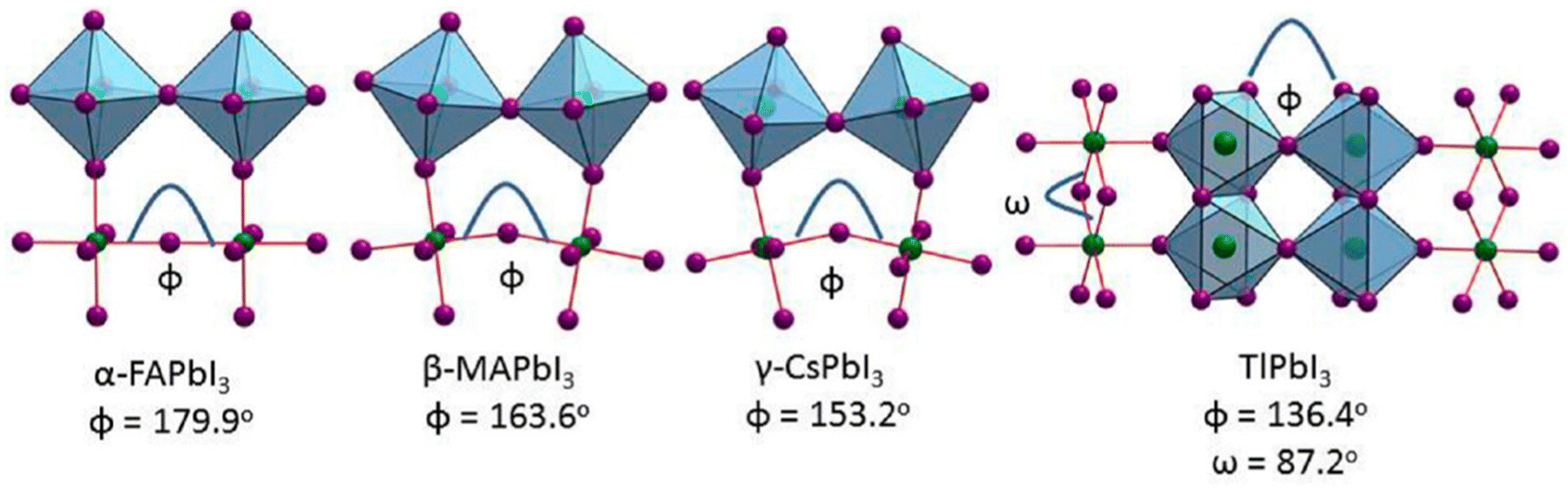 | ||
| Fig. 1 Crystal structures of the APbI3 series at room temperature for A = FA, MA, Cs, Tl, and NH4 cations, highlighting the effect of the structural distortions and the connectivity of the [PbI6]4− octahedra. Adapted with permission from ref. 51. | ||
The crystal structure stability of HPs can be predicted by calculating the so-called tolerance factor, 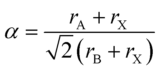
![[thin space (1/6-em)]](https://www.rsc.org/images/entities/char_2009.gif) 53,54 (with ri being the radii of i = A, B and X ions in the perovskite ABX3), which gives an estimate of the ionic size mismatches that a perovskite structure can tolerate until a different structure-type is formed. Both the performance and stability of inorganic–organic perovskite solar cells are limited by the size of the cations required for forming an appropriate lattice. It has been found that compounds with tolerance factors of a = 0.9–1.0 have an ideal cubic structure; a = 0.8–0.9 results in a distorted perovskite structure with octahedral tilting (usually orthorhombic), while when the tolerance factor is higher than 1 or lower than 0.8 non-perovskite structures are formed (Fig. 2a).55 It is common in the halide perovskite literature to denote the phase with a cubic structure as the α-phase and the phase with a non-perovskite structure as the δ-phase.51 Based on the above considerations, only three A+ cations known to date have tolerance values between 0.8 and 1 and are thus able to form a stabilized perovskite, namely Cs+, CH3NH3+ (MA), and HC(NH2)2+ (FA).56
53,54 (with ri being the radii of i = A, B and X ions in the perovskite ABX3), which gives an estimate of the ionic size mismatches that a perovskite structure can tolerate until a different structure-type is formed. Both the performance and stability of inorganic–organic perovskite solar cells are limited by the size of the cations required for forming an appropriate lattice. It has been found that compounds with tolerance factors of a = 0.9–1.0 have an ideal cubic structure; a = 0.8–0.9 results in a distorted perovskite structure with octahedral tilting (usually orthorhombic), while when the tolerance factor is higher than 1 or lower than 0.8 non-perovskite structures are formed (Fig. 2a).55 It is common in the halide perovskite literature to denote the phase with a cubic structure as the α-phase and the phase with a non-perovskite structure as the δ-phase.51 Based on the above considerations, only three A+ cations known to date have tolerance values between 0.8 and 1 and are thus able to form a stabilized perovskite, namely Cs+, CH3NH3+ (MA), and HC(NH2)2+ (FA).56
 | ||
| Fig. 2 (a) Correlations between the tolerance factor and crystal structure of perovskite materials. (b) Calculated energy difference between the α-phase and different δ-phases for FA1−xCsxPbI3 alloys with different Cs ratios. Adapted with permission from ref. 55. | ||
However, commonly used single-cation HPs present limitations due to their thermal or structural instabilities. MAPbI3, for example, the prototypical halide perovskite studied in PSCs, degrades fast upon exposure to light and moisture (the latter is due to the hygroscopic nature of the methylammonium cation), while it is also decomposed during annealing at 85 °C even in an inert atmosphere.57–59 On the other hand, despite being advantageous in terms of its bandgap (1.48 eV vs. 1.57 eV for MAPbI3)60 and thermal stability (it is relatively stable up to 150 °C in air), FAPbI3 suffers from severe structural instability at room temperature as it commonly crystallizes into a photoinactive, non-perovskite hexagonal δ-phase (“yellow phase”) instead of a photoactive perovskite α-phase (“black phase”); in addition, it is sensitive to solvents or humidity.61
A reasonable way to overcome the limitations of single-cation (and anion) HPs is the compositional engineering approach by mixing cations and halides in order to achieve perovskite compounds with improved thermal and structural stability.55 Intermixing different cations can combine the advantages of the constituents, while avoiding their drawbacks. Mixed cation 3D perovskites of the composition (MA)x(FA)1−xPbI3, where x = 0.6, delivered superior device performance when used as light-harvesting layers in mesoscopic solar cells.62 The mixed-cation composition with optimized stoichiometry MA0.6FA0.4PbI3 outperformed the single-cation compositions MAPbI3 and FAPbI3, while it also completely avoided the undesirable formation of the δ-phase, while maintaining the red-shifted band gap of FAPbI3. The superior carrier-collection efficiency was related to the longer exciton lifetime of more than 130 ns in the MA0.6FA0.4PbI3 material. These results showed that even a small amount of MA is sufficient to induce a preferable crystallization into the photoactive phase of the FA perovskite, resulting in a more thermally and structurally stable composition than the pure MA and FA compounds. This illustrates that the MA can be thought of as a “crystallizer” (or stabilizer) of the black phase FA perovskite. The fact however that MA is only slightly smaller than FA still permits a large fraction of the yellow phase to exist. Furthermore, by alloying FAPbI3 with CsPbI3, the tolerance factor can be effectively tuned, and the stability of the photoactive α-phase of the mixed FA1−xCsxPbI3 perovskite is significantly enhanced (Fig. 2b).55 These mixed cation perovskite films demonstrate much improved stability in a high-humidity environment and better solar cell performance and device stability than the FAPbI3 counterparts.
Moreover, the substitution of the larger I atoms with smaller Br ones in the mixed halide structure, MAPb(I1−xBrx)3, for x > 0.2, leads to the reduction of the lattice constant and a transition from the distorted tetragonal perovskite structure of pure MAPbI3 to the cubic perovskite structure of MAPbBr3, hence inducing advanced optoelectronic properties and superior PSC performance.63,64 Further intermixing both MA/FA cations and I/Br anions in an optimized (FAPbI3)0.85(MAPbBr3)0.15 perovskite structure stabilizes the perovskite phase and increases its crystallinity.65 As a step forward, intermixing Cs+, which has a considerably smaller ion than both MA+ and FA+, in a triple cation configuration Csx(MA0.17FA0.83)(100−x)Pb(I0.83Br0.17)3 provides additional versatility in fine-tuning high quality perovskite films that can yield stabilized PCEs.15 Incorporation of optimum amounts of Cs+ reduces the trap density by one order of magnitude, which is responsible for the increased VOC and FF, eventually leading to an enhancement in PCE. The triple cation perovskite films are less affected by temperature for a fixed halide ratio, while an increased Br content also contributes considerably to thermal stability. Cs+ induces the black phase of FA-based HPs at room temperature and better morphology as more uniform grains are formed that enable better charge transport, which in turn endows the fabricated devices with higher FFs. Moreover, alkali halide (NaX) additives effectively passivate both the organic cation and halide anion vacancies in the triple CsMAFA perovskite. Especially, sodium fluoride forms strong hydrogen bonds (N–H⋯F) with the organic (FA/MA) cations and strong ionic bonds with Pb in the triple perovskite film, protecting the materials from degradation and leading to long-term stability of the corresponding device.66
A pseudo-halide anion, formate (HCOO−), also improves the growth and crystallization of perovskite films.67 The insertion of FAHCOO into the precursor solution removes the halide vacancies in the FAPbI3 film, reducing the trap-assisted recombination. Consequently, formate results in an increase of FF, leading to higher PCE.68 Moreover, the elimination of deleterious lattice defects in FAPbI3, which can lead to degradation of the halide perovskite film, is beneficial for the operational stability of PSCs.
Furthermore, incorporation of traces of small radius rubidium (Rb) (rRb+ = 152 pm versus rCs+ = 167 pm) has been recently found to stabilize the black phase of FA perovskites.69 Whereas it is clear from the tolerance factor discussion above that Cs+ is the only elemental cation that is large enough to sustain the perovskite structure, Rb+ can still be integrated into PSCs, despite not being suitable as a pure RbPbI3 compound. PSCs based on perovskite materials bearing the rubidium cation along with caesium and/or organic cations have reached reasonable device performances.16 The outstanding maximum VOC of 1240 mV indicates a “loss in potential” (difference between VOC and the band gap) of only ∼0.39 V, which is one of the lowest recorded for any perovskite material, implying very small non-radiation recombination losses owing to its very low bulk and surface defect density. Moreover, it was observed that the charge transport within the RbCsMAFA perovskite layer is substantially faster than in CsMAFA, which is already much more defect-free than MAFA. Enhancement in charge extraction can also be achieved by reactive surface engineering of the perovskite layer. The creation of a built-in electric field in the surface of the perovskite film reduces surface recombination, which favors the improvement of the photovoltaic parameters.70
Halide perovskites exhibit a direct bandgap, which can be effectively tuned through compositional adjustment to allow absorption to reach the high energy frontier of the near infrared spectral region. The change in band gap observed with compositional adjustment, such as tailoring of halide concentration, can be explained as follows: the electronic states at the top of the valence band are mainly of halide p-character with a small contribution from metal s-orbitals (i.e., Pb 5s orbitals); those at the bottom of the conduction band are mainly derived from the metal p states (i.e., Pb 6p).50 The fully-occupied 5s orbital of Pb2+ has strong antibonding coupling with I 5p, making upper valence bands dispersive. The strong s–p antibonding coupling results in a small hole effective mass, which is comparable with electron effective mass, making MAPbI3-based perovskites ideal candidates for thin-film solar cells with a p–i–n configuration. The replacement of I− with Cl− or Br− leads to an increase in the band gap, due to the lower-lying Br-4p and Cl-3p electronic states that populate the top of the VB.71 In addition, the smaller dielectric constant associated with the larger bandgap in MAPbBr3 results in a larger binding energy, a smaller Bohr radius, a larger effective g-factor (i.e., a quantity that characterizes the magnetic moment and angular momentum of an atom or particle), and larger oscillator strength of the lowest-energy excitons in MAPbBr3 compared to those in MAPbI3.63
Due to the antibonding character and mixing of s and p orbitals to form band extrema, perovskites present only shallow defects, primarily A- and X-site vacancies, while interstitial and antisite defects, which would form detrimental deep trap states in the electronic structure, are almost absent.72 However, several types of extrinsic surface defects caused by unsaturated surface bonds and/or the surrounding environment are a major issue in grainy, polycrystalline HP films. For instance, X-terminating surfaces form traps due to the lack of local stoichiometric composition and improper surface bonding, which can be mitigated by introducing an appropriate passivation agent (PA). In an effective passivation scheme, new chemical bonds are formed at the perovskite surface and the derived orbitals shift the defect level either toward or into the band edges, hence suppressing the detrimental influence of the defect.73
In a similar manner, substitution of Pb with Sn lowers the conduction band bottom, hence reducing the bandgap due to the lower-lying Sn-p states (1.2–1.4 eV in Sn-based iodide perovskites as compared to 1.45–1.7 eV in Pb-iodide perovskites).51 This arises from the greater instability of the Sn2+ lone pair of electrons (residing in the s orbital), which in the octahedral coordination environment is pushed up in energy, creating broader bands than the corresponding Pb lone pair. In a first approximation, the MA cations do not contribute to the optical absorption, and their role is to act as a structural filler and to ensure the charge neutrality of the unit cell. However, they can affect the band gap energetics through steric and coulombic interactions, which may deform the perovskite lattice in a cation-specific way. On the other hand, mixed halide perovskites were found to be prone to photo-instability as photo-excitation during light-soaking was suggested to cause halide segregation into two crystalline phases, namely iodide-rich and bromide-rich domains, the former having a lower band gap and acting as a recombination trap centre, thus limiting the photovoltage attainable with these materials.
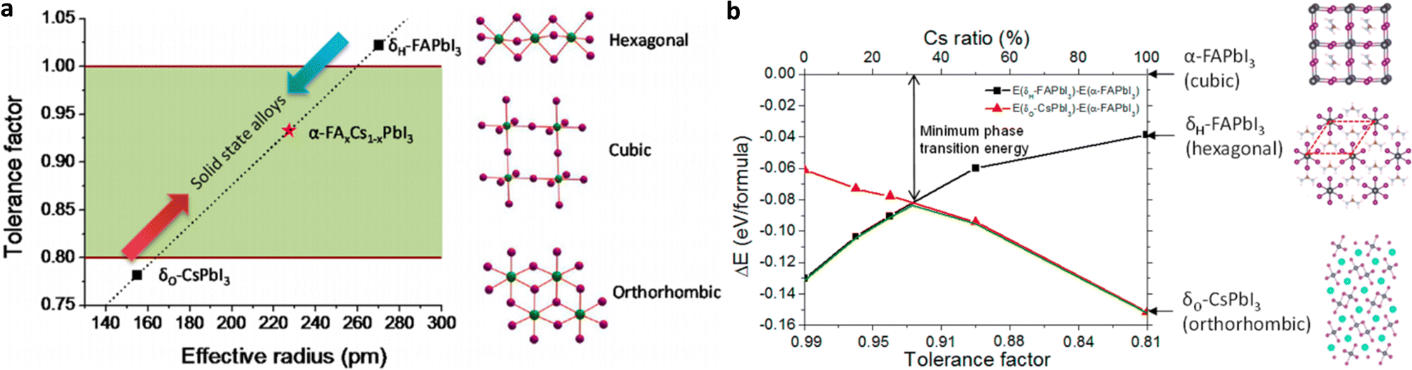
Two dimensional (2D) HPs can be generally described by the general formula L2An−1MnX3+1, where L is a large aliphatic or aromatic alkylammonium cation of the chemical type R-NH3, such as 2-phenylethylammonium (PEA) and n-butylammonium (n-BA).74 They are also known as Ruddlesden–Popper (RP) layered perovskites because they consist of alternative organic spacer and perovskite layers. Other structures of the 2D perovskites are the Dion–Jacobson (DJ) phase and the phase with alternating cations in the interlayer space (ACI), corresponding to the differences in crystallography and stacking motif, respectively.75 They are hence quite similar to conventional 2D materials having a van der Waals layered crystal structure. The (An−1MnX3n+1)2− part of their formula denotes the conductor layer that derives from the parent 3D (AMX3) perovskite. The MX6 octahedrons form the perovskite sub-layers that are sandwiched by the insulating organic spacers formed by the long chain molecular cations. The number of BX6 octahedrons and thus the thickness of each perovskite layer are defined by the n value (n = 1, 2, 3, 4,…) and can be adjusted by careful control of the stoichiometry.76
The incorporation of large organic spacers within their structure endows this class of HP materials with superior structural, thermal and moisture stability.77 Their structural stability is due to the strong van der Waals forces among the organic layers.78 Notably, the formation of even a small amount of a 2D perovskite structure can successfully inhibit the low-temperature phase transition of FAPbI3 and CsPbI3 perovskites, hence rendering α-FAPbI3 and α-CsPbI3 stable at room temperature.79 The moisture stability is due to the hydrophobic nature of the organic spacers, typically ammonium cations, that prohibit the water molecules from penetrating into the perovskite crystal lattice.80 In addition, ion migration, which is a severe limitation in PSCs based on 3D HPs, is not a great issue in 2D RP perovskites due to the higher activation energy of ion migration in 2D perovskites compared to 3D ones with similar compositions.81 Moreover, “edge states” that existed in perovskite layers when n > 2 can provide a direct pathway for dissociating excitons into longer-lived free carriers.
However, besides their exceptional overall stability, 2D HPs also present some not very appealing characteristics regarding their application in PSCs. The electrically insulating nature of the organic spacer and the high conductivity of the perovskite conductor layers give rise to a natural multiple-quantum-well structure: the perovskite layers serve as potential “wells”, while the organic spacer layers play the role of potential “walls”. This results in a weaker absorption ability of RP 2D perovskites within the visible spectrum due to their larger bandgap values compared to the 3D counterparts. For example, the bandgap (Eg) values of BA2MAn−1PbnI3n+1 and PEA2MAn−1PbnI3n+1 RP perovskites are 2.24 eV and 2.36 eV (for n = 1), respectively,82,83 while that of MAPbI3 is only 1.54 eV.84 Moreover, they present higher exciton binding energies (BEs), which make it more difficult for dissociation of excitons to photogenerated carriers to occur.85 Excitons in 2D HPs are generally considered as the Wannier-type and their BEs in a single layer (n = 1) RP perovskite are in the range of ∼157–480 meV (depending on the organic spacer, Fig. 3).86,87 This large exciton BE is much higher than the thermal energy at room temperature (kBT = 25.7 meV). Therefore, the photogenerated electron and hole pairs in RP HPs are strongly bound together by coulombic attraction. This is why the so-called excitonic absorption can be easily observed even at room temperature in these 2D perovskites in the form of a sharp peak below the bandgap onset. However, in most cases the excitonic absorption is merged with the absorption onset at room temperature, while at low temperatures this sharp peak is quite distinct.
 | ||
| Fig. 3 Views of the (a) (BA)2PbI4 single-layer (n = 1), (b) (BA)2(MA)2Pb3I10 three-layer (n = 3) 2D, and (c) MAPbI3 (n = ∞) 3D lead iodide perovskite crystal structures, highlighting their three-dimensional distortions. This figure illustrates the differences in the distortion modes of the n = 3 perovskite, emphasizing the in-plane and out-of-plane views of the perovskite slabs. Slabs belonging to different layers have been drawn in different colors (yellow, blue, green) to project the connectivity of the slabs in the third dimension. Adapted with permission from ref. 86. | ||
In addition, the insulating organic spacer largely prohibits carrier transport, hence inducing charge accumulation and non-radiative recombination at the conductor/insulator interface. Moreover, the charge extraction can also be hindered by the insulation of the organic spacers. The charge mobility is much higher in the direction along the perovskite slabs than in the direction perpendicular to the orientation of these slabs. To this end, for efficient 2D PSCs it is important to have perovskite slabs with the out-of plane orientation, so that thicker films with balanced charge transport and light absorption can be used to achieve a high PCE.
Because of these unfavorable characteristics, RP perovskite-based PSCs have lagged behind in efficiency compared to their 3D counterparts, and the goal of current research efforts is to maximize the efficiency without compromising their stability. For example, huge research efforts have been devoted to altering the composition of 2D perovskites, aiming to improve their optoelectronic properties. These also include molecular design of spacer cations, such as altering alkyl chain length,88 exposing ammonium dications,89 and inserting π-conjugated segments.90 Thus, a much wider range of optoelectronic properties can be tuned for 2D perovskites than for 3D analogues.
An attractive approach to tackle the limitations of lower absorption and limited charge transport of 2D HPs is their combination with the parent 3D structure. In fact, as the value of n in the perovskite formula increases above 10, HPs with properties similar to those of their corresponding 3D counterparts are obtained; yet these materials present features of 2D perovskites.91 Typically, the absorption onset of such perovskite materials combining the 2D and 3D structures is close to that of the corresponding 3D counterparts. Moreover, as the bandgap values of 2D perovskite phases are much larger than those of 3D ones, charges are highly confined to the 3D phase, hence overcoming the limitations of trapping and recombination at the interfaces between layers in the 2D phase, resulting in longer carrier lifetimes.92 Nevertheless, the presence of the 2D component endows their devices with exceptional stability and ultrahigh VOC values resulting in PCEs comparable to 3D ones, indicating them to be highly attractive candidates for PSCs. Finally, due to their highly hydrophobic nature and resilience to moisture, thin 2D perovskite films are also inserted as protective interlayers at either the bottom or top side of a 3D perovskite absorber.93
3. Synthetic approaches for polycrystalline perovskite films
The structural and optoelectronic properties of HPs are highly determined by the synthetic procedure adopted for their preparation. This is because only high-quality films can enable excellent intrinsic perovskite material characteristics to be fully exploited. A variety of synthetic procedures for 3D perovskites aiming to achieve high-quality perovskite films has been reported. They can be categorized into vacuum vapor deposition and solution processes.3.1 Vacuum deposition methods
With the vacuum deposition method, high-quality perovskite films and, consequently, high efficiency PSCs can be obtained. The perovskite films are prepared by co-evaporation of the two precursors, the inorganic metal halide (MX2 such as PbI2) and the organic halide salt (i.e., MAX, FAX, CsX, where X = I, Br, Cl). With this technique high quality perovskite films that exhibit satisfactory substrate coverage and uniformity within expectations can be constructed; such thin films are highly appropriate for planar junctions. For example, in 2013 Snaith and co-workers succeeded in achieving a record efficiency of 15% in planar PSCs by using a dual-source vapor deposition system to deposit MAPbI3−xClx perovskite films of superior quality by evaporating lead chloride (PbCl2) and methylammonium iodide (MAI) precursors simultaneously.94 However, this method requires the use of expensive vacuum facilities, thus increasing the device manufacturing cost. Moreover, it is not appropriate for the fabrication of mesoscopic PSCs, which requires the infiltration of the perovskite pigment onto mesoporous metal oxide.3.1.1.1 Single source and dual-source vapor deposition (VD). The easiest way to employ thermal evaporation is by one-step evaporation of the precursor material on top of the desired substrate. For example, the PbI2 and MAI precursor salts are placed inside metal boats, are evaporated simultaneously under vacuum conditions and then deposited on the desirable surface, which is then annealed for the film crystallization to be completed (Fig. 4a).95 However, this process requires careful adjustment of the deposition rate of each reagent, since the stoichiometry of the perovskite plays an important role in the efficiency of the final thin film.92 Another possibility would be for the MAPbI3 powder to be prepared before being placed inside the metal basket under vacuum conditions and evaporated.97 This would allow better control over the stoichiometry of the thin film, which would affect its properties. In both cases, this method offers the deposition of extremely uniform and pinhole-free films of adjusted thickness all over the substrate area.98 The improved uniformity of the perovskite film is very important to ensure successful fabrication of not only highly efficient small-size perovskite optoelectronic devices,99 but also of large-area devices.100,101
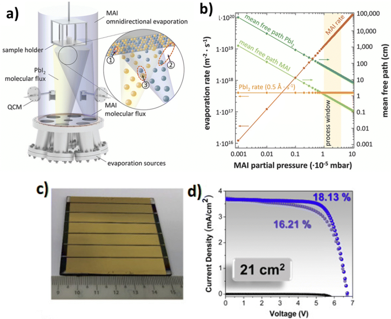 | ||
| Fig. 4 Schematic illustration of the employed evaporation system and chemical processes that can take place during the co-evaporation of PbI2 and MAI. (a) During co-evaporation three different reaction paths are conceivable: (1) a reaction of as-deposited PbI2 with MAI on the substrate, (2) a delayed reaction of as-deposited PbI2 with MAI from the environment, and (3) a reaction of PbI2 with MAI before reaching the substrate. (b) Theoretically expected evaporation rates and mean free paths of PbI2 and MAI in an omnidirectional process atmosphere as a result of the high vapor pressure and low evaporation enthalpy of MAI. Adapted with permission from ref. 95. (c) Image of a 21 cm2 active area PSM consisting of 6 series-connected sub-cells. (d) Treated-MAPbI3 PSM dark, forward, and backward J–V curves measured in air. Adapted with permission from ref. 99. | ||
3.1.1.2 Sequential evaporation. During sequential evaporation, PbI2 powder is first sublimed onto the substrate through the same process as the dual source technique. Following this, MAI reacts with the already deposited inorganic layer and forms the final thin film, accompanied by a color change (Fig. 5a–c). A major advantage of this sequential method is the highly smooth surface compared to solution processes, due to the first-deposited PbI2 film. Moreover, films created through a two-step process exhibit full surface coverage and high crystallization phase purity,101 because of the low-contamination deposition under vacuum conditions during the molecular time-of-flight. In any case, more perovskite films with better carrier-diffusion properties are fabricated with this method, since the size of the grains is larger and the control over the film properties is more effective through the control of each moiety separately.102 This layer-by-layer deposition is affected by physicochemical factors such as the temperature of the substrate, which, when not properly controlled, could result in non-stoichiometric films. It has been reported that the post-sublimation steps of the crystallization can be performed under ambient conditions so that this problem is avoided, since the air moisture contributes to the transformation of the unreacted MAI to MAPbI3.103 Unfortunately, in spite of the exceptionally uniform films and the high reproducibility that this technique offers, the cost of the infrastructure required for the perovskite formation is not a favorable factor towards its use on a larger scale. Nevertheless, Feng et al. demonstrated uniform large-scale Cs0.15FA0.85PbI3 perovskite films of high quality using a three-source layer-by-layer vacuum deposition method (Fig. 5d–f).104 The prepared perovskite films showed also large grain size and good crystallinity, resulting in highly efficient Cs0.15FA0.85PbI3-based solar cells with outstanding stability.
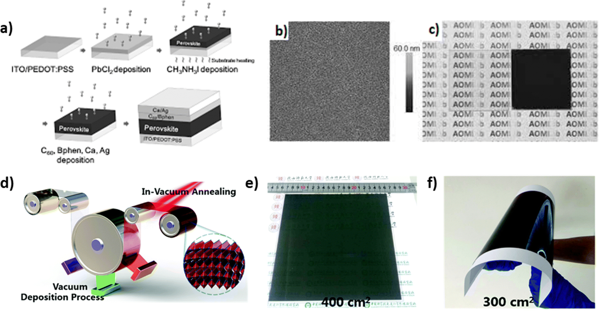 | ||
| Fig. 5 (a) Schematic illustration of perovskite solar cells fabricated by sequential layer-by-layer vacuum deposition. (b) AFM image (30 μm2) of the vacuum-deposited PbCl2 thin film. (c) Photographs of the vacuum deposited PbCl2 (left) and perovskite (right) thin films. Adapted with permission from ref. 102. (d) Schematic illustration of multisource vacuum deposition with an in-vacuum annealing process for large-area perovskite films. Photographs of FA-based perovskite films deposited on (e) glass and (f) PET substrates. Adapted with permission from ref. 104. | ||
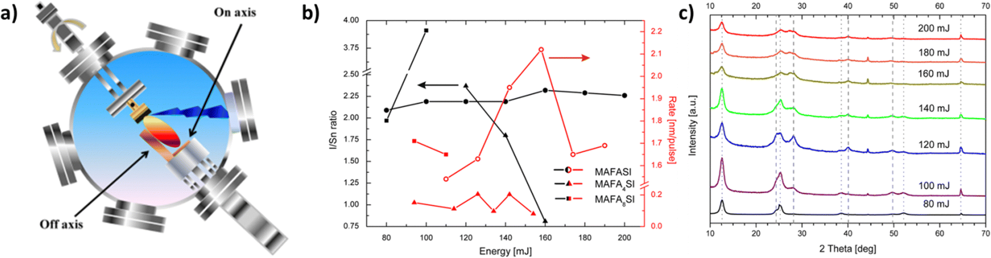 | ||
| Fig. 6 (a) Schematic representation and photograph of substrate arrangements for “on-axis” and “off-axis” deposition by pulsed laser deposition (PLD). Adapted with permission from ref. 107. (b) Ratio of iodine to tin (black symbols) and deposition rate (red symbols) as functions of energy density for MAFASI, MAFA4SI and MAFA8SI thin films. (c) Diffractograms of MAFASI thin films deposited at various energies, ranging from 80 to 200 mJ. The dotted lines indicate the positions of [001]-reflections of α-SnI2, while the dashed ones indicate the (111), (002), (022) and (222)-lattice planes of the perovskite structure from left to right, respectively. Note that the intensities are plotted on a linear scale. Adapted with permission from ref. 108. | ||
However, one possible disadvantage of PLD could be the non-uniform deposition of films, since re-evaporation takes place after the initial laser burst, which could be counterattacked by multiple laser pulses on top of the same substrate. Moreover, the amount of material deposited should gradually decrease with each pulse, so as to create the appropriate number and size of crystals inside the perovskite layer. In this way, one can gain control over the film thickness.105,106
Nevertheless, some additional difficulties may still arise in the case of organic–inorganic thin films caused by the different vaporization rate of each composing moiety, which in turn affects their deposition. Although this may be of little importance in conventional perovskite film fabrication,107 its consequences are more apparent in more complicated structures such as (NH2CH)1−x(CH3NH3)xSnI3 that shows enhanced thermal stability. As reported by Hoffmann-Urlaub et al.,108 the organic moiety creates a smoother surface on the film, because of its volatilization through plasma, while the inorganic moiety has a different morphology due to a different forming path, thus creating inhomogeneous areas on the substrate. This is why the target material should not be stoichiometric but its organic part is in excess.
In this way, it is obvious that many parameters should be controlled so as to fabricate large-grained thin films. Some of them would be the power of the beam, the pulse repetition rate, the deposition pressure and the substrate temperature (Fig. 6b and c). Such a procedure tailored to each deposition and subsequent high perovskite solar cell performance could be made possible through a two-step hybrid process.109 This technique for MAPbI3 perovskites involves the deposition of the lead halide through PLD onto the substrate and the subsequent addition of methyl ammonium iodide by spin-coating, followed by an annealing step. Through this process, an increase in grain size and control over film thickness are observed, minimizing any defects and increasing carrier mobility. In this way, the creation of highly crystalline and uniform films is possible, while the low temperature employed is promising for future fabrication under more flexible conditions.
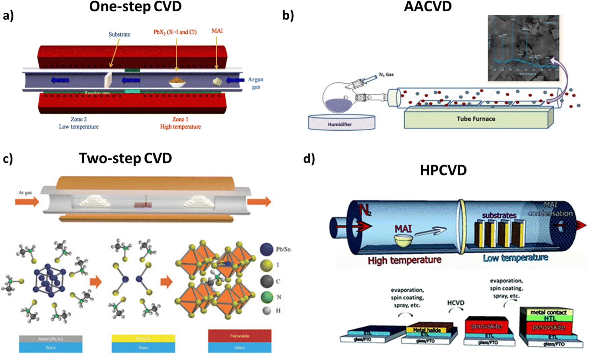 | ||
| Fig. 7 (a) Schematics of the perovskite film fabrication using MAI and PbX2 sources deposited onto a c-TiO2-coated FTO glass substrate which is performed in a CVD furnace. Adapted with permission from ref. 111. (b) Schematics of the all-inorganic perovskite CsPbBr2I by an aerosol assisted CVD method. Adapted with permission from ref. 116. (c) Schematic of the CVD furnace and growth conditions of a perovskite film, and schematics of reaction details of the metal film with MAI, resulting in perovskite film formation. Adapted with permission from ref. 118. (d) Hybrid chemical vapor deposition based perovskite synthesis (top) diagram of the HPCVD furnace and MAI deposition onto metal halide seeded substrates. (Bottom) Layered structure of a complete solar cell fabricated by a HPCVD process. The complete solar cell is a glass substrate followed by a FTO layer, an electron transport layer, a perovskite layer, a hole transport layer, and a top metal contact. Adapted with permission from ref. 120. | ||
3.1.3.1 One-step CVD. During one-step deposition, the organic and inorganic moieties in the gas phase of the perovskite thin film are simultaneously injected into a vacuum chamber, are co-evaporated and adsorbed on the preheated substrate. This method is quite helpful, since no secondary evaporation step is necessary and is a gas-only method.110 However, this method can also be applied in the case of mixed halide perovskites, producing pinhole-free CH3NH3PbI3−xClx films, containing PbCl2, PbI2 and MAI moieties, as far as planar cells are concerned (Fig. 8).113 In this case, the differences in vaporization time should be taken into consideration. The best results in terms of crystallinity are obtained with the use of argon as a gas carrier, at 360 °C evaporation temperature and 100 °C annealing temperature. In this way, perovskite films with larger grain size and longer carrier diffusion lengths can be obtained.
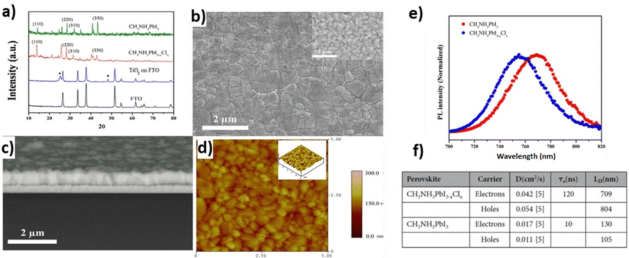 | ||
| Fig. 8 Structural characterization of the perovskite films deposited on c-TiO2-coated FTO substrates using the CVD method: (a) XRD patterns of FTO, the TiO2 film on the FTO substrate (the peaks labeled with “*” are from TiO2), CH3NH3PbI3−xClx and CH3NH3PbI3; (b) top-view secondary electron SEM image of a CH3NH3PbI3−xClx layer, with an inset showing a backscattered electron (BSE) image with higher resolution; (c) cross-sectional BSE SEM image of a CH3NH3PbI3−xClx layer; and (d) AFM height images (10 × 10 μm2), with an inset showing a 3D topographic image. (e) Photoluminescence spectra of lead halide perovskite films. (f) Carrier life-times and diffusion lengths of the perovskite films prepared by CVD which were derived from the time-resolved PL data. Adapted with permission from ref. 113. | ||
3.1.3.1.1 Aerosol assisted CVD. In this variation of the aforementioned method, the precursor mixture of the main gas flow is in the form of an aerosol, which is later decomposed during the deposition. For this method to be applied, the solvents and moieties used should be relatively volatile, making this variation a plausible deposition method for large-area substrates.115 This statement is also supported by the fact that AACVD takes place under ambient pressure, reducing the need for vacuum equipment. Unfortunately, perovskite solar cells fabricated through this method have shown low efficiency that originated mainly from the high surface roughness of the prepared perovskite film due to the large density changes during film formation.110,117
3.1.3.2 Two-step CVD. In the case of two-step deposition, each moiety is deposited separately on a substrate. At first, PbI2 is transferred into the quartz tube and consequently onto the substrate. The PbI2 coated substrate remains in the chamber, while a new flow of MAI vapor is injected, reacting with the already deposited thin film and thus forming the desired product. This allows the property tuning of each layer separately by gaining more control over the final film thickness and stoichiometry.
Two-step chemical vapor deposition can also be combined with the metal-alloying technique, in order to control better the film morphology. The team of Tavakoli et al.118 suggested a solvent-free process, where Pb and Sn metals are evaporated separately, forming an alloy layer with controlled thickness on top of the substrate, with the MAI vapor being deposited on top of the alloy layer under vacuum conditions. The engineering process of the alloy composition enables the creation of a eutectic mixture which, in turn, enhances the quality of perovskite films through large-sized grains in the uniform film (Fig. 9).
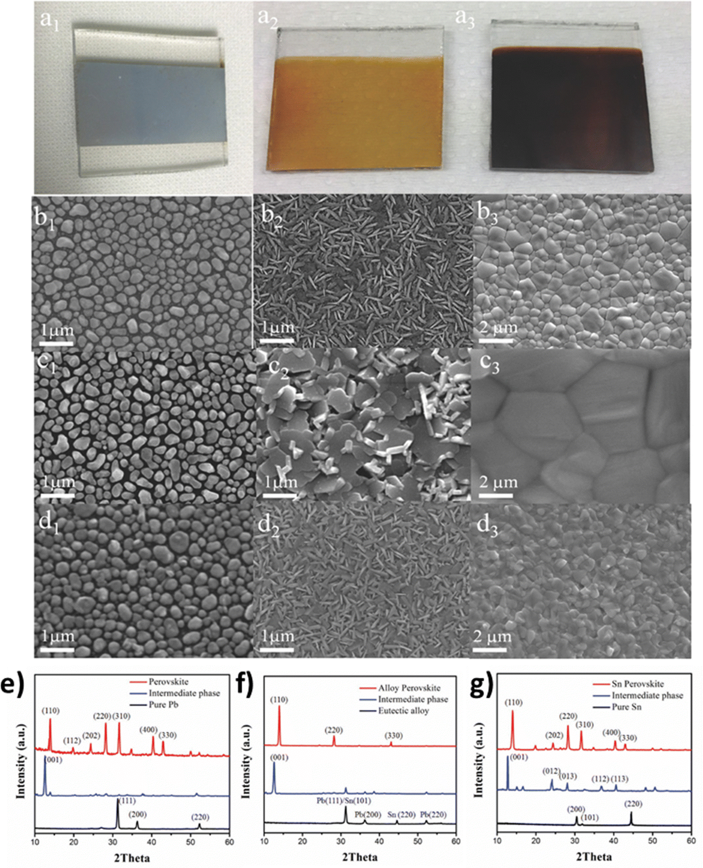 | ||
| Fig. 9 Photographs of substrates after (a1) deposition of the metal alloy, and after reaction times of (a2) 20 min (intermediate SnI2/PbI2 phase) and (a3) 40 min (perovskite film). Top-view SEM images of the (b1) Pb metal, (c1) eutectic alloy film, and (d1) Sn metal; and intermediate phases for the (b2) Pb, (c2) eutectic alloy, and (d2) Sn formed after 20 min reaction time; and perovskite films for the (b3) Pb, (c3) eutectic alloy, and (d3) Sn after 40 min reaction time. X-Ray diffraction patterns of metal films, intermediate phases after 20 min reaction, and perovskite films formed by the reaction between the metal precursor and MAI after 40 min, for different metal precursors (e) pure Pb, (f) the eutectic alloy, and (g) pure Sn. Adapted with permission from ref. 118. | ||
3.1.3.2.1 Low-pressure CVD. A variation of two-step CVD employing milder conditions is low-pressure CVD, which is a slow solid–gas reaction. This method, promising for future scalability of perovskite optoelectronic devices, involves the deposition of a PbI2 thin layer on top of the substrate through spin-coating. Subsequently, the covered substrate and CH3NH3I powder are placed at different positions and at different temperatures inside a tubular furnace. The two moieties react with each other and are finally annealed under ambient conditions. The derived films show strong absorption and satisfactory stability, while the method itself requires less energy consumption and more cost-friendly machinery.112
3.1.3.3 Hybrid physical–chemical vapor deposition (HPCVD). In the previous sections, we described the differences between thermal evaporation and chemical evaporation techniques. In some cases, however, there is a combination of both methods applied during the formation of organic–inorganic thin films through a hybrid chemical evaporation procedure. More specifically, thermal evaporation under high vacuum conditions is employed for the deposition of the metal halide, while the addition of the organic moiety on top of the already covered substrate through chemical vapor deposition follows. By all means, during the deposition steps, the substrate is maintained under low pressure and temperatures below 170 °C and the post-annealing steps take place under ambient conditions, for the deposition to be uniform and without any defects.119 The advantage of this two-step fabrication would be control over the thickness and the uniformity of the film because of the vacuum thermal evaporation (VTE) process, as well as better nucleation and crystallization through the MAI moiety diffusion on top of the substrate on the gas phase.120,121 Recently, crystalline CsPbBr3 films were prepared with a two-step hybrid CVD process. In order to increase the quality of the perovskite films, the reaction temperature was set between 310and 360 °C.122 The same conditions were also reported for the fabrication of scaled-up modules, with the economical aspect taken into consideration.123 Qiu et al. demonstrated the fabrication of large area perovskite solar cells, where the FA-Cs mixed perovskite layer was deposited via a hybrid CVD process.124 Upon increasing the area of the cell by a factor of 1000, a slight reduction of the device performance was obtained, suggesting that hybrid CVD is a promising method for scalable perovskite optoelectronic devices. Table 1 summarizes the electrical parameters of perovskite solar cells based on vacuum deposition methods for the preparation of the perovskite absorption layer.
| Method | Perovskite | J SC (mA cm−2) | V OC (V) | FF | PCE (%) | Ref. |
|---|---|---|---|---|---|---|
| Vapor-deposition | MAPbI3−xClx | 21.5 | 1.07 | 0.67 | 15.4 | 94 |
| Vapor-deposition | MAPbI3 | 21.6 | 1.08 | 0.83 | 19.5 | 97 |
| Physical vapor-deposition | MAPbI3 | 19.47 | 0.932 | 0.60 | 10.9 | 98 |
| Thermal evaporation | MAPbI3 | 16.12 | 1.05 | 0.67 | 12.04 | 99 |
| Co-evaporation | MAPbI3 | 23.3 | 1.12 | 0.777 | 20.28 | 100 |
| Sequential evaporation | CsPbBr3 | 7.59 | 1.328 | 0.752 | 7.58 | 101 |
| Sequential evaporation | CH3NH3PbI3−xClx | 20.89 | 1.02 | 0.722 | 15.4 | 102 |
| Vacuum deposition | Cs0.15FA0.85PbI3 | 24.88 | 1.11 | 0.772 | 21.32 | 104 |
| Pulsed laser deposition | CH3NH3PbI3−xClx | — | — | — | 7.7 | 107 |
| Pulsed laser deposition | MAPbI3 | — | — | — | 1.12 | 109 |
| LPCVD | MAPbI3 | 21.7 | 0.91 | 0.645 | 12.73 | 112 |
| One-step CVD | CH3NH3PbI3−xClx | 18 | 0.97 | 0.64 | 11.1 | 113 |
| One-step CVD | MAPbI3 | 15.9 | 0.95 | 0.61 | 9.2 | 113 |
| AACVD | MAPbI3 | 16.1 | 0.77 | 0.44 | 5.42 | 117 |
| CVD | MAPbxSn1−xI3 | 25.5 | 0.796 | 0.692 | 14.04 | 118 |
| Hybrid evaporation | MAPbI3 | 13.14 | 1.029 | 0.4267 | 5.77 | 119 |
| Hybrid CVD | CH3NH3PbI3−xClx | 19.1 | 0.92 | 0.62 | 10.8 | 120 |
| HPCVD | MAPbI3 | 18.58 | 1.00 | 0.66 | 12.3 | 121 |
| Hybrid CVD | CsPbBr3 | 4.85 | 1.39 | 0.65 | 4.41 | 122 |
| LPHCVD | MAPbI3 | 18.20 | 0.991 | 0.72 | 13.52 | 123 |
| HCVD | Cs0.1FA0.9PbI2.9Br0.1 | 20.2 | 0.90 | 0.67 | 12.3 | 124 |
3.2 Solution deposition approaches
In the early attempts, deposition was sufficiently accomplished in a single step using a common solution of PbI2 and MAI precursors.125 However, the lack of suitable solvents that can dissolve both components and the high perovskite reaction rate resulted in large morphological variations and therefore in large deviations in the achieved efficiencies. In 2013, Grätzel and co-workers described a sequential deposition method for the successful infiltration of the perovskite pigment within a porous TiO2 film.126 In particular, lead iodide (PbI2) was first introduced via spin coating from solution into the nanoporous TiO2 film and subsequently dipped into a solution of methyl ammonium iodide (MAI) to synthesize the resultant MAPbI3 perovskite film. It was found that the conversion to the perovskite occurred within the nanoporous oxide as soon as the two precursors came into contact, hence allowing for better control over the morphology and reproducibility of perovskite films. As a result, solid-state mesoscopic perovskite solar cells with a high efficiency of 15% were obtained, thus providing new opportunities for the fabrication of solution-processed mesoscopic PSCs. However, this method is not very convenient for the preparation of planar devices because it often results in films with significant surface roughness that frequently peel off from the substrate.1273.2.1.1 One step spin-coating. During the one-step process, organic halides along with metal halides are mixed with an appropriate solvent, forming the precursor solution. Mostly aprotic polar solvents, such as N,N-dimethylformamide (DMF), dimethyl sulfoxide (DMSO), γ-butyrolactone (GBL), 2-methoxyethanol (2-ME) and acetonitrile (ACN), are used, which exhibit high boiling point and low vapor pressure when at room temperature.128 The solution formed is subsequently deposited on the substrate surface on top of the electron transport layer in standard architecture solar cells. This substrate is placed on a spin-coater and spun at high rotational speeds for a couple of seconds so that the excess solvent evaporates. During the evaporation, the creation of the perovskite layers takes place, with crystals being formed and grown due to the ionic interaction between metal cations and halogen anions.129 The substrate is finally annealed at a temperature between 80 and 150 °C for 10 minutes to 2 hours, so that the remaining solvent is removed.130 A similar technique to this is hot casting, during which the mixture of the organic and inorganic solutes is first heated at 70 °C and subsequently deposited on an already heated substrate at 180 °C. The substrate is then put in a spin-coater and finally annealed on a hot plate, which leads to the development of millimeter-scale crystallites.131
Even though this method may appear to be quite simple, there are some problems found within it. The uniformity of the perovskite layer, crucial to its light harvesting properties, is dependent on factors such as annealing conditions. As reported by Wang et al.,132 fast crystallization due to accelerated solvent evaporation leads to incomplete pore filling, while Li et al.133 suggested that low-volatile organic components need higher temperatures to be driven out, thus creating defects in the film. A solution to this problem would be a solvent-induced crystallization method, in which a second solvent is added to the substrate before the annealing step so as to induce the nucleation process, resulting in the formation of large crystals.134 However, even if such a methodology is employed, the thickness of the film and the possible grain boundaries should be taken into consideration with a more elaborate method being employed.129
3.2.1.2 Two-step spin-coating. To overcome the aforementioned defects, a two-step spin-coating method is proposed as a better alternative. The metal halide mixed with the appropriate solvent, usually DMF, is first deposited on the bottom electrode material and subsequently subjected to spin-coating followed by annealing under the conditions mentioned above. In the next step, the organic halide moiety is dissolved in a solvent, where the organic halide exhibits low solubility and is deposited on top of the dried metal halide layer. Then the already prepared metal halide film is placed on the spin-coater and thermally annealed in a similar fashion. In this way, the first layer is converted into the desirable perovskite film. The morphology of the final film can be adjusted by the manipulation of spinning speed and deposition time.133,134Fig. 10a illustrates the one-step and two-step coating procedures of CH3NH3PbI3 on mesoporous TiO2 substrates. In the two-step deposition, the perovskite film fills the TiO2 pores, resulting in a void-free CH3NH3PbI3 layer, while in the one-step deposition the formation of perovskite islands is clearly seen (Fig. 10b and c).
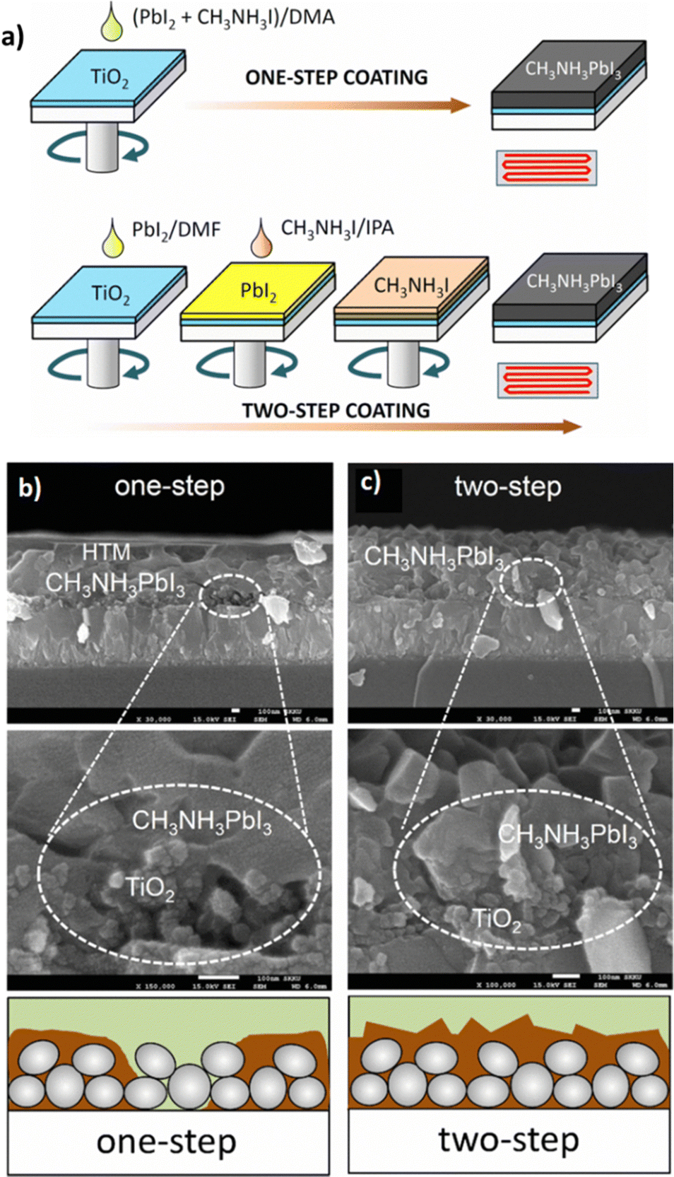 | ||
| Fig. 10 (a) One-step and two-step spin-coating procedures for CH3NH3PbI3 formation. PbI2 was mixed with CH3NH3I in N,N-dimethylacetamide (DMA), which was spin-coated and heated for one-step coating. For two-step coating, a PbI2-dissolved N,N-dimethylformamide (DMF) solution was first spin-coated on the substrate, dried and then a CH3NH3I-dissolved isopropyl alcohol (IPA) solution was spin-coated on the PbI2 coated substrate. Cross-sectional SEM images of (b) one-step deposition of CH3NH3PbI3 and (c) two-step deposition of CH3NH3PbI3. One-step deposition leads to imperfect pore-filling as shown in the high magnification SEM image. Two-step deposition results in the pores of the TiO2 layer being fully filled with CH3NH3PbI3 as confirmed by the void-free CH3NH3PbI3 layer. Adapted with permission from ref. 135. | ||
The two-step method has also been proved to solve the hysteresis effect in a planar device, since the homogeneity of the film minimizes the existence of defects and charge traps. Moreover, it is more cost effective in terms of materials than the one-step deposition method, since the quantity of the second solution is adjusted according to the concentration of the metal halide solution. Thus, the thickness of the second deposited film depends on the thickness of the first one, which supports their immediate reaction upon contact.135,136
This deposition method was also used for the creation of larger-scale perovskite thin films. Mei et al.141 reported the creation of a TiO2/ZrO2 scaffold in which the perovskite solution could enter through drop casting. This solution, containing PbI2, CH3NH3I, 5-ammonium valeric acid iodide (5-AVAI) and γ-butyrolactone as a solvent, led to the creation of a perovskite with stoichiometry (5-AVA)x(MA)1−xPbI3. This ameliorated the contact with the TiO2, so as to create a layer with fewer defects, enhanced performance and promising reproducibility on a 10 cm × 10 cm substrate. This type of device structure, employing carbon as a back contact, seems also to have enhanced stability under continuous illumination under outdoor conditions.142 In a recent work, 2DRP perovskite films were prepared by using the drop-casting method without any further processing step such as antisolvent treatment or inert-gas blowing. For large-scale perovskite solar cell fabrication, a slot-die coating system was used to deposit a homogeneous and compact perovskite film on a 25 mm × 25 mm PET/ITO/PEDOT:PSS substrate. The fabricated device achieved a power conversion efficiency of 8.8%, which was lower compared with that based on a perovskite film drop-cast on a glass/ITO/PEDOT:PSS substrate due to the higher sheet resistance of the PET/ITO.143
According to this technique, the evolution of the film starts with the construction of the inorganic framework of the perovskite material by a solution process, and subsequently an in situ reaction between the inorganic species and the desired organic vapors takes place, forming the perovskite film.147 A crucial factor to the formation of the film is the source temperature that creates the appropriate vapor pressure so as not to damage or decompose the gaseous halide salts completely. The substrate temperature will also affect the dynamics of the perovskite formation. In other words, the VASP exploits the kinetic reactivity of the organic vapor and the thermodynamic stability of the perovskite during the in situ growth process. Hence, the advantage that this technique has over pure vacuum and solution processing is the intercalation of the organic components into the inorganic framework through vapor, as it prevents the high growth rate of the perovskite material during the co-deposition of precursors and the degradation of the latter upon dipping the inorganic framework into an organic solution. In sum, the VASP can provide perovskite films with full substrate coverage, small surface roughness and well-defined grain sizes up to the microscale. Chen et al.147 reported the formation of CH3NH3PbI3 (MAPbI3) films on mesoporous TiO2 by means of a vapor-assisted solution method for use in solar cells. The cross-sectional SEM images showed that the VASP fabricated MAPbI3 films exhibited a continuous capping layer with a flat surface, yielding better optical and electrical properties and hence higher power conversion efficiency as compared to solution deposited perovskite films (Fig. 11a). In addition, Sedighi et al.148 employed the VASP approach to prepare mixed halide perovskites (CH3NH3PbI3−xXx) in an ambient atmosphere for solar cell fabrication, as well. The perovskite films were synthesized by exposing PbI2 to CH3NH3X (where X = I, Br, or Cl) vapor. The final films exhibited good crystallization (Fig. 11b), particularly CH3NH3PbI3, while the inclusion of chlorine and bromine into the perovskite lattice led not only to lower temperature and shorter reaction time but also to smaller grains (Fig. 11c–e) and surface roughness.
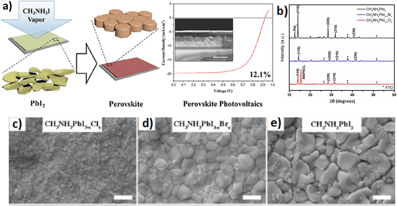 | ||
| Fig. 11 (a) Schematic illustration of perovskite film formation through a vapor-assisted solution process. Adapted with permission from ref. 147. (b) XRD patterns for films of CH3NH3PbI3, CH3NH3PbI3−xBrx, and CH3NH3PbI3−xClx deposited by the VASP method. FTO = fluorine-doped tin oxide. SEM surface images of (c) CH3NH3PbI3−xClx, (d) CH3NH3PbI3−xBrx, and (e) CH3NH3PbI3 deposited by the VASP method. Scale bars are 500 nm. Adapted with permission from ref. 148. | ||
Recently, high-performance perovskite solar cells with PCEs of ∼21% were demonstrated using methylammonium chloride (MACl) vapor in order to improve the quality of the MAPbI3 layer and increase its grain size.149 In another work, solar devices with a planar structure of fluorine-doped tin oxide (FTO)/compact-TiO2/C60/(FA)x(MA)1−xPbI3/spiro-OMeTAD/Au with different MA:FA mixed cation ratios were fabricated by Chen et al.150 The formation of the mixed perovskite films was achieved by heating the PbI2 coated substrates with the FAI and MAI powders uniformly applied around them at 170 °C for 30 min under low vacuum. Their best planar device revealed a PCE of 16.48%. Furthermore, 2D/3D mixed perovskite films were developed using a low-pressure VASP, where phenylethylammonium iodide (PEAI) was added in PbI2 and then the prepared film was reacted with methylamine (CH3NH2(g) and MA(g) vapors).151 It was demonstrated that the 3D MAPbI3 perovskite was formed on the surface of multiple 2D RP perovskite layers of PEA2MAn−1PbnX3n+1 with different n values, suggesting a vertical-gradient phase distribution, which could be effectively applied in perovskite optoelectronic devices. Moreover, quasi-2D PEA2(FAPbBr3)n−1PbBr4 films prepared through the VASP were incorporated in perovskite light-emitting diodes, exhibiting not only high luminance and external quantum efficiency, but also good reproducibility.152 In a moderate concentration DMSO-vapor environment, a smooth perovskite film with uniformly distributed nanograins was formed, showing an enhanced photoluminescence quantum yield and quenched nonradiative recombination. DMSO-vapor also plays a crucial role in the crystallinity and growth of the perovskite film in order to form a high-quality and pin-hole free perovskite layer. Shadabroo et al.153 showed that DMSO vapor-annealing treatment of Cs2AgBiB6 was beneficial to the performance of Pb-free all-inorganic perovskite solar cells.
Today, hydrothermal synthesis refers to the synthesis of substances by chemical reactions in a sealed heated aqueous solution at appropriate temperature (100–1000 °C) and pressure (1–100 MPa).155,156 According to reaction temperature, hydrothermal synthesis is classified into two categories: subcritical and supercritical synthesis reactions. A subcritical synthesis reaction is carried out in the temperature range of 100–240 °C, while a supercritical synthesis reaction occurs at much higher temperatures. In addition, according to the vapor pressure of the main composition in the reaction, either low-pressure or high-pressure conditions can be employed to control the morphological features of the as-made materials. The uniqueness of this technique stems from the fact that any stable precursor used in the process can break at relatively low temperature, thus preventing the extensive agglomeration that solid-state reactions generally cause at high sintering temperature. Consequently, other problems encountered with high-temperature processes, like poor stoichiometry control due to the volatilization of components, can be avoided. Moreover, another factor that distinguishes hydrothermal synthesis from other conventional synthesis methods is that it is a rather environmentally benign method which may be attributed, apart from the low processing temperatures, to the absence of milling and the ability to recycle or dispose waste that cannot be recycled.157
Nowadays, hydrothermal synthesis is linked to several interdisciplinary branches of science, favoring the preparation of numerous advanced materials158 including perovskites.159 Given the fact that hydrothermal synthesis permits rapid mixing of precursors for homogeneous products with controllable parameters, it has become one of the most preferable and adaptable chemical routes to prepare homogeneous perovskite films. In 2012, the Peng group160 first demonstrated the synthesis of CH3NH3PbBr3 and CH3NH3PbI3 by mixing lead acetate with HI/HBr solution and methylamine alcohol solution and then heated at 150 °C in an oven for 1–12 h. The hydrothermally grown microcrystals were used as the active material in Li-ion batteries, presenting a discharge capacity of 331.8 mA h g−1 (at a current density of 200 mA g−1). Fig. 12a–c shows the SEM image and the corresponding EDX spectrum of the hydrothermally prepared CH3NH3PbBr3 along with the cycling performance of the Li-ion batteries based on the CH3NH3PbI3 and CH3NH3PbBr3 perovskites. Mahmood et al.161 reported the synthesis of lead iodide (PbI2) micro-needles using a hydrothermal method in the presence of surfactant cetyltrimethylammonium bromide (CTAB) at a low temperature of 100 °C for 8 h. Highly crystalline MAPbl3 micro-needles were produced by covering the surface of PbI2 micro-needles using an isopropanol solution of CH3NH3I (MAI) that resulted in a pin-hole free perovskite solar cell yielding a PCE of 17.98%, as shown in Fig. 12d. All-inorganic based cesium lead-halide (CsPbX3) was also synthesized by a hydrothermal method.162 In particular, CsPbI3 and CsPb2Br5 powders were hydrothermally prepared and then deposited via a spin-step spin-coating method to form the active layer of perovskite solar cells. Hydrothermally developed CsPbI3 and CsPb2Br5 crystals formed highly crystalline nanowires and nanorods, respectively, as shown in SEM images of Fig. 12e and f. Both δ-CsPbI3 and tetragonal CsPb2Br5 nanostructures were PL active with unique optical properties, suggesting their successful use in Cs-based perovskite optoelectronic devices.162
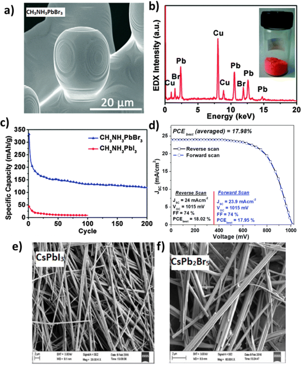 | ||
| Fig. 12 (a) SEM image of hydrothermally synthesized CH3NH3PbBr3 and (b) the corresponding EDX spectrum with the photograph of CH3NH3PbBr3 inset. (c) Cycling performances of the Li-ion batteries made of perovskite CH3NH3PbBr3 and CH3NH3PbI3. Adapted with permission from ref. 160. (d) J–V curves (in both the forward and reverse scans) for the best-performing device with MAPbI3 micro-needles. Adapted with permission from ref. 161. FE-SEM images of (e) high quality yellow phase CsPbI3 nanowires and (f) highly crystalline CsPb2Br5 nanorods. Adapted with permission from ref. 162. | ||
Unfortunately, there has been little research related to one-step preparation of mixed-metal oxides via the solvothermal method.168,169 These functional materials, having provided the momentum for a large number of technological applications, usually contain one or more transition-metal elements, whose oxidation states are pivotal in dictating their underlying properties (i.e. electronic, magnetic or redox properties).170 Perovskites containing transition metals exhibit constructive properties derived from the control of certain oxidation states. Nevertheless, controlling crystal morphology in terms of particle shape and size is also crucial for the use of solvothermal synthesis. Lately, a number of studies have demonstrated the benefit of solution-mediated crystallization of multinary oxides containing metals whose oxides are volatile, which can be prevented without affecting the stoichiometry of the precursors. In most of the cases, it has been shown that the crystallization of materials could be attained by the use of solvents.162 The solvent medium is linked to the solubility of the reactants and, apart from its contribution to the nucleation process by bringing the precursors, it may lead to the crystallization of the final product without the need for high concentrations of hydroxide salts. In this regard, apt selection of the precursor composition and reaction conditions can result in very homogeneous particles with a narrow size distribution.171,172 Crystalline CH3NH3PbI3 was prepared via a solvothermal method for the first time in 2015, where the crystal growth depended on the temperature and reaction time.173 Recently, all-inorganic perovskites have also been solvothermally synthesized. Zhai et al.174 showed that by modifying the solvothermal reaction sources, the versatility of perovskite crystal structure could occur, demonstrating phase transformation from cubic CsPbBr3 nanoplatelets to rhombohedral Cs4PbBr6 nanocrystals, and vice versa. The solvothermal method was also proved as a successful procedure for Mn-doped CsPbX3 perovskite quantum dots and nanoplatelets. It was shown that controllable solvothermal reaction conditions and most importantly the Cs-to-Pb feeding ratio were crucial to the perovskite preparation.175,176 Furthermore, high-quality CsPbX3 nanowires prepared by the solvothermal method exhibited good crystallinity and a high photoluminescence quantum yield. Consequently, the incorporation of CsPbI3 in photodetectors was beneficial to the device performance, achieving fast light response speed and a high switching ratio.177
Moreover, self-assembled CsPbBr3 nanowires prepared by a two-step solvothermal procedure and a direct-dripping method showed unique polarization characteristics.178 Interestingly, excitation polarization-dependent emission was demonstrated, attributed to the anisotropic charge distribution of the perovskite nanowires. More recently, a new approach to solvothermal preparation of CsPbBr3 nanowires was demonstrated, using short-chain ligand engineering in order to improve the photoelectric properties of the perovskite. The prepared nanowires exhibited excellent uniformity, a good photoluminescence lifetime and high mobility.179
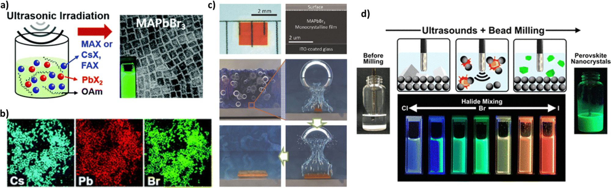 | ||
| Fig. 13 (a) Ultrasound-induced synthesis of APbX3 perovskite nanocrystals with a wide range of compositions, where A = CH3NH3, Cs, or HN=CHNH3 (formamidinium), and X = Cl, Br, or I. (b) EDX maps showing homogeneous distributions of Cs, Pb, and Br in CsPbBr3 NCs. Adapted with permission from ref. 186. (c) Optical image of the monocrystalline film (left). Cross-sectional SEM image of a freshly cut monocrystalline film (right). Illustrations of the CTAC mechanism on a microscopic scale. Adapted with permission from ref. 187. (d) Schematic illustration of the ultrasound-assisted bead milling (top) and photograph under a UV lamp of the colloidal halide-mixed perovskite nanocrystals. Adapted with permission from ref. 189. | ||
Peng et al.187 used ultrasonication to grow CH3NH3PbBr3 (MAPbBr3) monocrystalline films of various thicknesses for perovskite solar cells. By exploiting the perovskite's tendency to crystallize in solution, they designed a novel growth method termed cavitation-triggered asymmetrical crystallization (CTAC) to aid heterogeneous nucleation via the introduction of a very short ultrasonic pulse (≈1 s) into the solution when it reached a low supersaturation level, thus overcoming the limitations of conventional single-crystal growth techniques due to their propensity to create solely free-standing perovskite single crystals. At high supersaturation levels, cavitation triggered immoderate nucleation and thus the growth of numerous small-scale crystals. Fig. 13c shows an optical image and a cross-sectional SEM image of the monocrystalline film (left and right, respectively). Lately, ultrasound assisted synthesis was used to prepare high-quality perovskite quantum dots (QDs).
Chen et al.188 presented in their research work that ultrasonic irradiation, apart from its use in accelerating the precipitation of perovskite quantum dots, contributed to the crystallization process of QDs providing particles of smaller sizes with a narrower size distribution. They also prepared perovskite quantum dots with different chemical compositions that led to an immensely wide color gamut. In addition, the photoluminescence peak intensity can be controlled by adjusting the halide component in the perovskite precursor through an ultrasound-assisted bead milling method (UBM).189Fig. 13d illustrates the perovskite MAPbBr3 QD preparation and the different colors emitted under UV irradiation. Purification of red-emissive MAPbI3 QDs prepared by UBM using different carboxylate esters resulted in minimizing the particle size distribution and thus improving the optical properties of perovskite QDs. When purified MAPbI3 QDs were incorporated in light emitting devices, an excellent external quantum efficiency was obtained.190
One of the most effective ways to form better crystals is by temperature tuning. Several approaches of synthetic protocols have been proposed for hybrid perovskites ranging from two-step processes to direct crystallization.26,197,198 Although perovskites have the merit of being deposited from their precursors into a thin film by solution-based processes, it is rather difficult to gain control over the nucleation and crystallization of the as-prepared film from a saturated solution by evaporation of the solvent. The procedure of crystallization is affected by a number of variables like an oxygen-rich atmosphere and humidity that may cause a compounding effect of crystal sizes and surface chemistries.199 Both chemical and physical properties can be adjusted at the atomic level via the use of reactants and thermal annealing. The most popular procedure to initiate crystallization of perovskite films is thermal annealing at 100 °C for 10 min. Thereafter, different thermal annealing processes have been reported such as high-temperature thermal annealing,200 multistep thermal annealing201 and laser induced thermal annealing.202 However, aside from the aforementioned thermal annealing processes, it has been shown that the microwave irradiation process can lead to a faster crystallization of the perovskite material requiring less energy.203 In fact, the implementation of microwave irradiation as a thermal initiator can lead to the crystallization of the perovskite material within few minutes, thus making microwave assisted synthesis one of the most promising synthetic routes towards the generation of hybrid perovskites. During optimization experiments, it has been found that the applied microwave power is pivotal to both crystallinity and device efficiency.204 Tuning the irradiation time changes not only the crystallization of the synthesized perovskite, but also the photoluminescence emission and quantum yield.205 However, prolonged exposure to microwave irradiation will lead to the opposite result. Another factor that plays a crucial role in the preparation of perovskites under microwave irradiation is the solvent. In order to point out how critical the effect of solvents is on perovskite materials, Cao et al.198 mixed PbI2–CH3NH3I adducts with different solvents, including DMF, DMSO and diethyl ether. It was noticed that while the adducts added to DMF or DMSO would turn black when irradiated, the mixed PbI2–CH3NH3I added to diethyl ether did not change to black, indicating that the latter could not absorb the radiation and convert it into heat. The change in the color of the mixed PbI2–CH3NH3I added to DMF or DMSO suggested that the solvents could absorb energy, convert it into heat and thus accelerate the perovskite precursors to react at the atomic level and crystallize. In fact, according to their research, the grain size of perovskite films revealed a trend of linear increase between the time of microwave treatment and different time intervals.
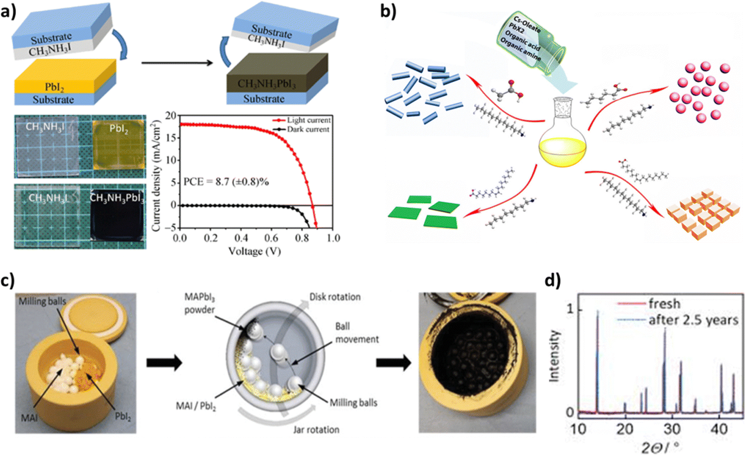 | ||
| Fig. 14 (a) Schematic illustration of the fabrication process of perovskite films using a solid-state reaction (top) and the corresponding photographs of the real films (bottom-left). The J–V curves of the perovskite solar cells prepared using the solid-state chemical reaction method under AM 1.5G irradiation and in the dark (bottom-right). Adapted with permission from ref. 210. (b) Schematic illustrating the formation processes for different CsPbX3 (where X = Cl, Br, I) nanocrystals mediated by organic acid and amine ligands at room temperature: hexanoic acid and octylamine for spherical quantum dots; oleic acid and dodecylamine for nanocubes; acetate acid and dodecylamine for nanorods; and oleic acid and octylamine for few-unit-cell-thick nanoplatelets. Adapted with permission from ref. 222. (c) Photograph of a milling jar loaded with milling balls, MAI, and PbI2 precursor powders (left), schematic of the ball milling procedure for the mechanochemical synthesis of perovskite powders (middle), and photograph of the milling jar after the ball milling process and successful mechanochemical synthesis of black MAPbI3 powder (right). (d) XRD patterns of MAPbI3 powders before and after more than two and a half years of storage in a dry atmosphere. Adapted with permission from ref. 237. | ||
As mentioned, the interdiffusion step of this process includes annealing at high temperatures. A high temperature of above 100 °C is most commonly applied because effective diffusion between the two precursor films is impeded by the kinetically unfavourable van der Waals gap in the interface between them. However, the necessity of applying higher annealing temperature to enable the diffusion entails consuming more energy and creating more non-radiative defects in the final film. It is thus possible to shorten the diffusion distance through the use of a nanoporous PbI2 film or a less crystallized nanoporous one, so that lower temperatures can be applied. In nanoporous films, the diffusion distance is determined by the size of particles and not the bulk film thickness, while the larger surface area accelerates the reaction. In this way, the temperature employed can be decreased to 75 °C.211
A main advantage of this solid-state reaction method is that there is no need for orthogonal solvents during the film fabrication and that the final film is compact with minimal surface roughness. Moreover, no careful control of the ratio of the two precursor salts is required in order to form stoichiometric perovskites. The sole controlling parameters of the reaction in question are the quantity of CH3NH3I and the reaction time, both of which should be sufficient enough to let the PbI2 film be converted into CH3NH3PbI3. Any CH3NH3I excess can be removed via both the annealing step and the removal of the top substrate, which creates the possibility that it could be reused in another deposition process. Finally, the solid-state reaction method shows potential for a future-scale up, thanks to the reproducibility of this process as well as lack of solvents.207,210
Indeed, in the case of perovskites, their crystallization process is controlled by the supersaturation induced by the solubility change with solvent mixing. More specifically, after the initial perovskite precursor salts are dissolved in a suitable highly polar aprotic solvent, a non-polar solvent is added. The precursor ions are insoluble in the latter, leading to the production of a highly supersaturated state which results in the crystallization of perovskite material in the mutually mixed solution. Considering that multiple ions bond together to create the final perovskite structure, the precipitation reaction is often called co-precipitation, since it implies the simultaneous precipitation of ions from the precursor salts. However, in the case of techniques employed for the synthesis of perovskite crystals, the term used is anti-solvent precipitation.212
It is worthwhile to note that there are certain combinations of solvents with anti-solvents used for the precipitation method to take place effectively, producing compact and uniform perovskite films. As a general rule, solvents in which perovskite precursor salts have poor solubility, such as chlorobenzene (CB), toluene (TL) and diethyl ether (DE), seem to be most commonly employed as anti-solvents, even though many other green antisolvents, such as ethanol and ethyl acetate, have been probed.215–217 According to Paek et al.,218 the critical parameters to decide on an appropriate anti-solvent are its miscibility, high boiling point, and dielectric constant (with a value of >5). Moreover, according to the anti-solvent employed in each synthesis, the quantity dripped and the point of dripping during spin coating tend to differ and need to be optimized appropriately.
The ligand-assisted reprecipitation technique involves two steps. In the first step, the perovskite precursors and ligands are added in a “good” polar solvent such as dimethylformamide (DMF), tetrahydrofuran (THF) or dimethyl sulfoxide (DMSO). The dissolution of precursor salts and molecule ligands is favored by polar solvents. For the fabrication of CH3NH3PbBr3 nanoparticles, the salts used are CH3NH3Br and PbBr2, the ligands added are a medium-to-long chain alkyl ammonium bromide, such as octylamine, and oleic acid, while octadecene was also incorporated in the solution as a noncoordinating solvent. The solution is then stirred and heated at 60–80 °C until it becomes colorless. In the second step, a “bad” non-polar solvent in which the perovskite materials are slightly soluble, such as toluene, acetone or hexane, is added to the aforementioned solution, while rigorous stirring follows. The poor solubility of the perovskite precursor salt ions in such solvents promotes their reprecipitation and the formation of the desired products as solids at the bottom of the reaction flask, with solution colour changes indicating the identity of the reaction products. The mixture is finally cooled and centrifuged in order to collect the desired nanocrystals.220–222Fig. 14b illustrates the formation processes for different CsPbX3 nanocrystals, such as nanorods, quantum dots, nanocubes and nanoplatelets.
A similar method to LARP is the hot-injection method, requiring higher temperatures in the 80–200 °C range. In this type of synthesis two solutions containing precursor salts and ligands need to be prepared. In order to fabricate CsPbX3 nanocrystals, cesium acetate and oleic acid are dissolved in hexadecane at 120 °C, thus forming cesium oleate solution. For preparing the second solution, PbX2 is added to octadecene and the mixture is dried under vacuum at 120 °C. After drying, a capping ligand mixture of dried oleylamine and oleic acid at a 1:1 ratio as is injected in a N2 atmosphere. After PbX2 has been dissolved, the temperature is raised to 140–200 °C for tuning the nanocrystals’ size. The cesium oleate solution is then injected into the second solution, with perovskite crystals forming instantaneously. The solution is cooled in an ice bath and then subjected to centrifugation, resulting in the final perovskite crystals.223 For the fabrication of other perovskite crystals, such as FAPbBr3 with formamidinium instead of cesium, formamidinium acetate is added in lieu of cesium acetate and heated at 130 °C, thus forming FA-oleate as the first reaction solution. Another more complex approach for synthesizing FAPbBr3 nanocrystals incorporating oleylammonium bromide and CH3MgBr precursors was proposed by Protesescu et al., with the former precursor producing brightly-luminescent cubic-shaped nanocrystals.224
The use of long alkyl chain ammonium cations as capping ligands on the surfaces of nanoparticles is a strategy enabling control over their size and morphology, by preventing the formation of nanostructures other than the desired. Octylamine, along with longer chain amines such as dodecylamine and hexadecylamine, is used to control the kinetics of the crystallization by slowing down the crystallization rate of the precursors. On the other hand, the use of oleic acid or other long chain alkyl acids, such as octanoic acid and butyric acid, involves the stabilization of the colloidal solution under storage conditions, by suppressing the aggregation of nanocrystals. This leads to the crystallization of perovskite moieties into colloidal nanoparticles in a controlled way.
Through the reprecipitation reaction assisted by ligands, it is possible to synthesize a variety of perovskite nanostructures in solution, including zero-dimensional spherical quantum dots, nanocubes, one-dimensional nanorods and two-dimensional nanoplatelets. This is especially pertinent to CsPbX3 perovskites. For each nanostructure, a different organic acid and an amine as capping ligands are employed in order to control the size and morphology of the final product. More specifically, along with the polar solvent and the perovskite precursor salts, hexanoic acid and octylamine were added in order to create spherical quantum dots. Similarly, oleic acid and dodecylamine were employed for nanocubes, acetate acid and dodecylamine for nanorods and oleic acid and octylamine for few-unit-cell-thick nanoplatelets.222
Another application of the hot-injection and LARP methods is the creation of quantum dots in a wide color range. By using salt precursors with different halogen anions and tunable compositions, a range of brightly luminescent colloidal CsPbX3 and CH3NH3PbX3 quantum dots with high photoluminescence quantum yield values above 70% can be fabricated. In this way, color tuning is performed, since the absorption and photoluminescence maxima vary according to the X-moiety incorporated.225
The main advantage of the LARP method over the hot-injection method is that it is performed at moderate temperatures below 70 °C. This also comes in contrast to other techniques requiring heating at high temperatures, such as vacuum ones. Moreover, there are minimal equipment requirements compared to the hot-injection method, where the rate of injection and the inert atmosphere need to be modified accordingly, making it a low-cost technique with scale-up potential. Another benefit is the dispersion of the perovskite product in a colloidal solution medium, making its further deposition on substrates simple.226 In addition, lead-free perovskite films and nanocrystals, such as CsSnX3, can be easily prepared through the LARP method in the same way as their counterparts containing lead.227
Besides PbO2, PbS has also been used as a precursor for the preparation of MAPbI3. Luo et al.232 electrodeposited PbS and then a MAI CVD process was used for the successful conversion into the desired black perovskite film. More importantly, the authors managed to develop high-quality, curved and large-area MAPbI3 films, which are promising for large-area perovskite optoelectronic devices. In a recent work, a Pb film was electrodeposited on mesoporous titanium oxide (m-TiO2) and then MAI was deposited atop.233 MAPbI3 was formed in a MAI/isopropanol solution by adjusting the time of reaction. In addition, the incorporation of the MAPbI3 films in mesoscopic perovskite solar cells led to high values of the electrical parameters, making electrodeposition a feasible method for preparing homogeneous and uniform perovskite films for perovskite-based devices.
Moreover, electrochemical deposition has been applied to prepare all-inorganic perovskite films, as well. For the formation of CsPbBr3, Pb was deposited on mesoporous TiO2 in PbI2/isopropanol solution, and then it was converted into CsPbBr3 perovskite in a CsBr/methanol solution.234 The reaction was performed in air at room temperature under a positive bias. The deposition current and time of the PbI2 during the first-step of the method were the important factors for the control of the grain size and film thickness of the synthesized perovskite. On the other hand, the crystallinity of the CsPbBr3 film was affected by the second-step-conversion voltage and time. CsPb2−xBr1+x was also prepared by immersing an electrodeposited PbO2 in HI/ethanol solution to form as already mentioned the PbI2 film. The preparation of the perovskite film was completed via spin-coating CsBr solution in methanol. The authors demonstrated that the addition of a small amount of DMF in the CsBr/methanol solution improved the perovskite film formation and crystallinity, and thus the efficiency of the fabricated perovskite solar cells based on the synthesized CsPb2−xBr1+x.
3.3 Mechanochemical synthesis
Mechanochemical synthesis is a solid-state solvent-free method for halide perovskite preparation. In this method a mixture of AX and BX2 (e.g., MAI, MABr, FAI, and CsI, and PbI2 and PbBr2) precursor powders are placed together in a ball mill235 or in a simpler approach in a portal,236 and ground until the corresponding perovskite is formed. In order to prepare a cleaner crystalline perovskite, ball milling is the best strategy that avoids remains of unreacted precursors that might exist due to pestling. The balls and bowls are usually made of stainless steel or zirconia. During the reaction, energy transfer from the balls to the precursor powders occurs, crushing the reactant materials and forming the perovskite with a simultaneous color change. Fig. 14c shows the mechanochemically synthesized MAPbI3 powder along with the change in color from yellow to black. Thus critical parameters for the size and crystallinity of the prepared perovskite are the bowl rotation speed, the number of milling balls, and the reaction energy.237Over the last decade, various halide perovskites have been synthesized via a mechanochemical method including hybrid organic–inorganic perovskites with MA+ or FA+ as the organic compound and I−, Br− or Cl− as the X− halide anion238–240 and all-inorganic CsPbX3 perovskites.241–245 Moreover, mechanochemically synthesized Pb-free perovskites based on Sn,246,247 copper (Cu)248 and bismuth (Bi)249 have been demonstrated. Interestingly, the use of CsCl as precursor powder led to the successful preparation of multiple-cation perovskite materials, solving the problem of the poor solubility of some cesium halides in traditional DMSO and DMF solvents.250Table 2 summarizes the electrical parameters of solar cells based on solution-processed and mechanochemically synthesized perovskites.
| Method | Perovskite | J SC (mA cm−2) | V OC (V) | FF | PCE (%) | Ref. |
|---|---|---|---|---|---|---|
| Dip-cast | MAPbI3 | 17.1 | 0.992 | 0.73 | 12.9 | 126 |
| One-step spin-coating | MAPbI3 | 21.2 | 0.96 | 0.74 | 16.7 | 127 |
| Hot-casting spin-coating | PbCH3NH3I3−xClx | 22.4 | 0.92 | 0.82 | 16.9 | 131 |
| Drop-cast | Cs0.1Rb0.05FA0.85PbI3 | 22.69 | 0.909 | 0.786 | 16.21 | 132 |
| Two-step spin-coating | MAPbI3 | 16.50 | 0.97 | 0.66 | 10.58 | 133 |
| One-step spin-coating | MAPbI3 | 21.1 | 1.04 | 0.63 | 13.8 | 134 |
| Two-step spin-coating | CH3NH3PbI3 | 21.47 | 1.024 | 0.634 | 13.9 | 135 |
| Two-step spin-coating | MAPbI3 | 19.6 | 0.99 | 0.793 | 15.4 | 136 |
| Drop-cast | MAPbI3 | 22.76 | 1.08 | 0.7563 | 18.57 | 139 |
| Drop-cast | (5-AVA)x(MA)1−xPbI3 | 22.8 | 0.858 | 0.66 | 12.84 | 141 |
| Drop-cast | (5-AVA)x(MA)1−xPbI3 | 22.7 | 0.85 | 0.66 | 12.9 | 142 |
| Slot-die | (C4A)2MA4Pb5I16 | 15.58 | 1.08 | 0.52 | 8.75 | 143 |
| VASP | MAPbI3 | 19.8 | 0.924 | 0.663 | 12.1 | 147 |
| VASP | CH3NH3PbI3 | 19.9 | 0.90 | 0.76 | 13.5 | 148 |
| VASP | CH3NH3PbI3−xClx | 15.1 | 1.11 | 0.69 | 11.6 | 148 |
| VASP | CH3NH3PbI3−xBrx | 14.2 | 1.07 | 0.69 | 10.5 | 148 |
| VASP | (FA)x(MA)1−xPbI3 | 22.51 | 1.00 | 0.7356 | 16.48 | 150 |
| Hydrothermal | Cs2AgBiBr6 | 3.96 | 0.98 | 0.624 | 2.43 | 153 |
| Hydrothermal | MAPbI3 | 24 | 1.015 | 0.74 | 18.02 | 160 |
| Hydrothermal | δ-CsPbI3 | 2 | 0.55 | 0.66 | 0.74 | 162 |
| Hydrothermal | α-CsPbI3 | 13.8 | 0.94 | 0.52 | 6.90 | 162 |
| Hydrothermal | CsPb2Br5 | 5.7 | 0.82 | 0.59 | 2.82 | 162 |
| Ultrasound-assisted | MAPbBr3 | 6.69 | 1.36 | 0.69 | 6.53 | 187 |
| Microwave-assisted | MAPbI3 | 21.9 | 1.041 | 0.735 | 16.8 | 199 |
| Solid-state reaction | MAPbI3 | 22.49 | 1.08 | 0.67 | 16.21 | 206 |
| Solid-state reaction | MAPbI3 | 19.6 | 1.00 | 0.747 | 14.7 | 207 |
| Solid-state reaction | MAPbI3 | 22.20 | 1.01 | 0.6808 | 15.21 | 209 |
| Solid-state reaction | MAPbI3 | 17.9 | 0.87 | 0.643 | 10.00 | 210 |
| Low-temperature solid-state reaction | MAPbI3 | 22.5 | 0.956 | 0.642 | 13.8 | 211 |
| Anti-solvent dripping technique | Cs0.15FA0.85PbI3 | 24.26 | 1.05 | 0.7635 | 21.53 | 215 |
| Anti-solvent treatment | MAPbI3 | 22.2 | 1.082 | 0.74 | 17.75 | 216 |
| Anti-solvent treatment | MAPbI3 | 24.48 | 1.12 | 0.7695 | 21.09 | 217 |
| Anti-solvent treatment | MAPbI3 | 23.3 | 1.10 | 0.79 | 20.3 | 218 |
| Electrodeposition | MAPbI3 | 19.1 | 0.97 | 0.55 | 10.19 | 228 |
| Vapor-assisted chemical bath deposition | MAPbI3 | — | — | — | 4.68 | 232 |
| Electrochemical deposition | MAPbI3 | 23.24 | 0.92 | 0.663 | 14.33 | 233 |
| Electrochemical deposition | CsPbBr3 | 8.85 | 1.43 | 0.62 | 7.86 | 234 |
| Mechanochemical synthesis | (Cs0.05FA0.95PbI3)0.85(MAPbBr3)0.15 | 16.8 | 1.00 | 0.74 | 12.4 | 237 |
| Mechanochemical synthesis | FAI/PbI2/MABr/PbBr2/CsCl | 22.54 | 1.16 | 0.711 | 19.12 | 250 |
One of the main advantages of mechanochemically synthesized perovskites is their high stability, making them promising candidates for perovskite optoelectronic devices. It is demonstrated that FAPbI3 and CsPbI3 prepared via a mechanochemical method directly crystallize into the desired black α-phase and more slowly degrade into the yellow δ-phase compared to the corresponding solution-processed perovskites.237,251 MAPbI3 also shows outstanding stability when stored in dry nitrogen for 2.5 years, as revealed by X-ray diffraction measurements presented in Fig. 14d.237 Furthermore, the same perovskite powder was thermally stable when exposed to 160 °C for 11 h and humidity conditions, as well. Moreover, a mechanochemical process was applied for upscale synthesis of perovskite powders. Recently, Tang et al.252 reported the synthesis of 100 g MAPb(IxBr1−x)3 and MAPb(BrxCl1−x)3 powders using ball milling and MAPbX3 precursors. Hong et al.237 synthesized 250 g of CsSnX3 powder and used it for the fabrication of perovskite photodetectors based on a completely solvent-free protocol, suggesting the successful development of perovskite devices with reduced environmental and energetic footprints.
4. Growth of single crystals and the corresponding layers
There are several techniques that have been used so far, to grow single-crystal (SC) halide perovskites. The method that is used is very important, since the quality of the crystal is a defining factor in scientific and industrial applications. In this section the corresponding methods for perovskite single-crystal growth and the formation of the corresponding layers are summarized.4.1 Growth of perovskite crystals
Perovskite single crystals have gained enormous attention in recent years due to their facile synthesis and excellent optoelectronic properties. The synthetic approaches adopted for the growth of perovskite single crystals, particularly through solution-based growth, are described in the following sections.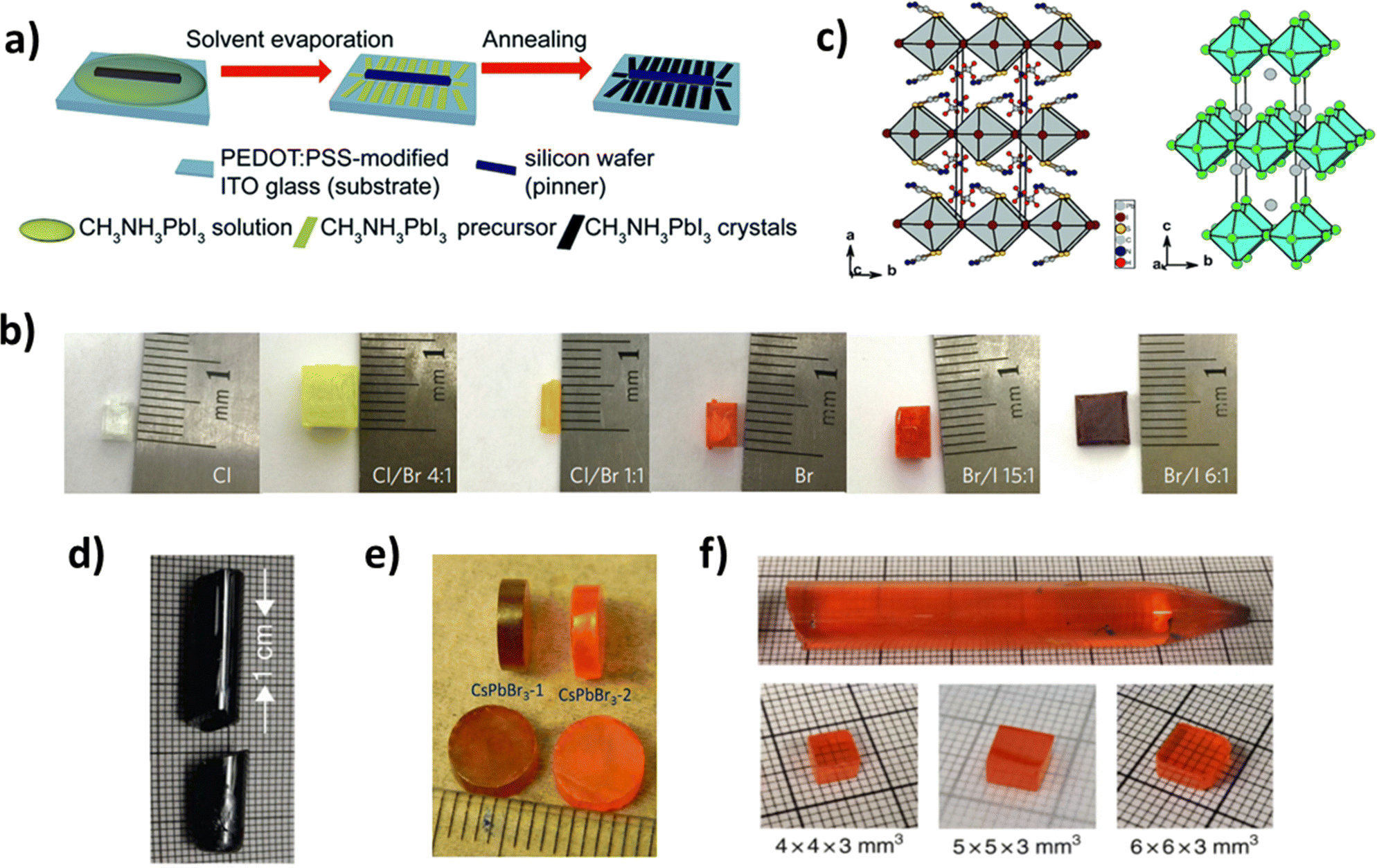 | ||
| Fig. 15 (a) Schematic of the growth process of CH3NH3PbI3 arrays. Adapted with permission from ref. 249. (b) Photographs of single-halide and mixed-halide perovskite SCs with different halide compositions. Adapted with permission from ref. 3. (c) Crystal structures of (CH3NH3)2Pb(SCN)2I2 (left) and K2NiF4 (right). Adapted with permission from ref. 46. (d) CsSnI3 SCs grown in a Bridgman furnace. Adapted with permission from ref. 264. (e) Photograph of the SC specimens: CsPbBr3-1 and CsPbBr3-2. Adapted with permission from ref. 255. (f) As-grown SC ingot with a diameter of 11mm, and the single crystal wafers with different sizes. Adapted with permission from ref. 263. | ||
mm3. The tunability of the hybrid organo-plumbates makes it easy to customize the band gap and the visible absorbance for an appropriate application in photovoltaics through cation and halide replacement. Daub et al. used this method for the reaction of CH3NH3I with Pb(SCN)2 in order to grow (CH3NH3)2Pb(SCN)2I2 crystals, with a structure that was similar to the K2NiF4-type as seen in Fig. 15c.46
minutes and then cooling at room temperature. First Rodova et al.261 and later Stoumpos et al.262 grew CsPbBr3 SC perovskites with the same method (Fig. 15e), mainly as promising candidate materials for X- and γ-ray radiation detection. The CsPbBr3 SCs were prepared from equimolar amounts of CsBr and PbBr2 that were transferred to a sealed silica ampoule and then gradually annealed up to 600 °C for 6 hours under vacuum and then left to cool at room temperature.
More recently, He et al. managed to grow CsPbBr3 SCs as well, with a modified melt growth method. They obtained large SC ingots that were crack-free with a purity of lower than 10 ppm of total impurities and a low defect density.263 In order to form polycrystalline CsPbBr3, both CsBr and PbBr2 were mixed in a stoichiometric ratio of 1:1 at 580 °C. The synthesis and growth were both done in the same silica tube, in order to reduce contaminations that may develop in a multistep process, where the tube that was used had 11 mm inner diameter, with a conical shaped end, as shown in Fig. 15f. Zhang et al. reported also the growth of CsPbBr3 SCs using a modified Bridgman method.264 A quartz ampoule with an inner diameter of 24 mm, filled with 170 g of polycrystalline CsPbBr3, was transferred to a 2-zone Bridgman furnace. The high and low temperature zones of the furnace were 600 °C and 200 °C, respectively, and the gradient of the temperature was 30–40 °C cm−1. The ampoule was heated in the high temperature zone for 12 hours and then was cooled slowly, at 1 mm h−1. Finally, the furnace was cooled to room temperature during 3 days and a large crack-free SC of CsPbBr3 was obtained.
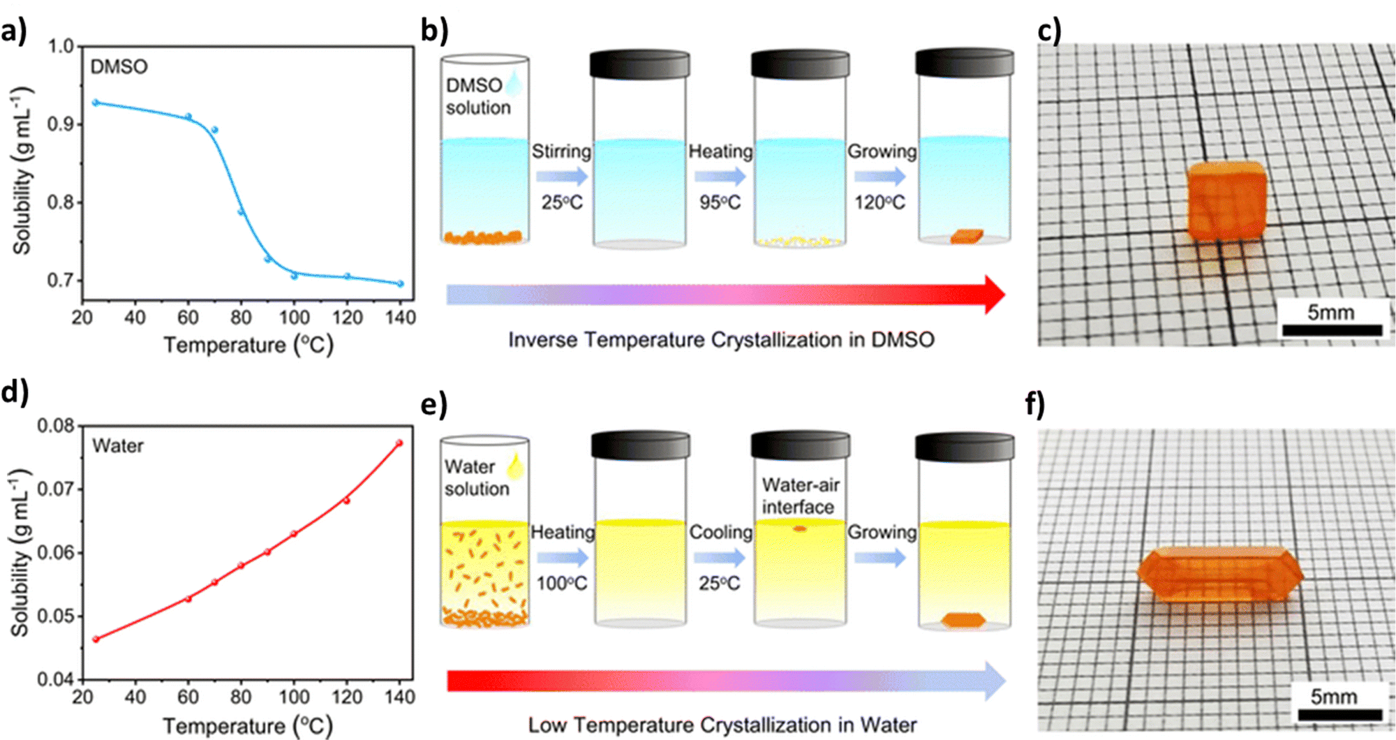 | ||
| Fig. 16 (a) Temperature-dependent solubility of CsPbBr3 in DMSO. (b) Schematic illustration of the inverse-temperature crystallization in DMSO. (c) Optical image of the as-prepared CsPbBr3 SC. (d) Temperature-dependent solubility of CsPbBr3 in water. (e) Schematic illustration of the low-temperature crystallization in water. (f) Optical image of the as-prepared CsPbBr3 SC. Adapted with permission from ref. 266. | ||
Saidaminov et al.49 investigated the influence of different solvents at various temperatures on the preparation of MAPbX3 and FAPbX3 SCs, suggesting that GBL and DMF were suitable solvents for ITC growth of I- and Br-based perovskites, respectively. In the same context, MAPbI3 was synthesized via the ITC method using GBL solvent.47 The solution was first prepared at 100 °C under vigorous stirring, and then the temperature was increased to 190 °C in order to form the perovskite crystals. Afterwards, the temperature was decreased to 25 °C, leading to undesirable dissolution of the synthesized SCs. Recently, a large-sized MAPbI3 SC was formed with the ITC method and the anisotropic properties at the surface and bulk of the SC were investigated.267 Parikh et al. suggested that the (112) facet of the MAPbI3 SC exhibited higher trap density than the (100) facet, resulting in higher hysteresis. Furthermore, low trap density along with high mobility was reported for the MAPbBr3 SC based photodetector.88 The proposed ITC method used a low dissolution process, forming high-crystalline-quality perovskite SCs, which played a critical role in the photoresponse of the fabricated SC devices.
All-inorganic perovskite and mixed cation SCs were also prepared using ITC growth. For instance, large-sized orange colored CsPbBr3 crystals were grown using ternary solvents, where DMF and GBL or cyclohexanol were used to improve the solubility of the perovskite in DMSO.268,269 Furthermore, a mixed cation (FAPbI3)0.9(MAPbBr3)0.05(CsPbBr3)0.05 single crystal was grown in a GBL solution heated at 95 °C.44 Interestingly, the prepared SC exhibited high stability upon light and water/oxygen exposure for 1000 h and 10000 h, respectively. Recently, high performance perovskite solar cells based on a mixed cation FA0.6MA0.4PbI3 SC were reported. The ability of the prepared SC, used as the absorption layer, to red-shift the external quantum efficiency spectrum increased the short-circuit current density of the device, exhibiting a high PCE of 22.8%.270 In addition, Pb-free perovskite SCs, such as MASnI3, were synthesized via an ITC procedure.271 A 2 mm × 1 mm × 1.2 mm MASnI3 without a sign of Sn(IV) in the crystal, as revealed by X-ray photoelectron spectroscopy, exhibited good crystalline properties, along with high optical absorbance, making it a promising material for solar cell fabrication.
MITC is a useful method to grow all-inorganic SCs. Especially, synthesis of pure CsPbBr3 SCs can be achieved by avoiding undesirable impure crystals formed due to the poor solubility of CsBr.275,276 Recently, CsPbBr3 was prepared through MITC using water as solvent. The solubility of the crystals at various temperatures was investigated, and the structural and electronic properties of the SCs were studied and compared with those of the CsPbBr3 crystal synthesized in DMSO.267Fig. 16d–f illustrates the growth of SC perovskites via a MITC process. More recently, Cl-doping of CsPbBr3 SCs grown via the MITC method was proposed to improve the photoelectric properties of the perovskite.277 Reduced trap density and improved carrier mobility were reported for the CsPbBr2.5Cl0.5 SC compared with the undoped perovskite crystal, along with the high sensitivity of X-ray detectors, when the Cl-doped SCs were incorporated in the device. Pb-free all-inorganic perovskite SCs were also synthesized using the MITC process, such as CsCu2I3.278 The 1D CsCu2I3 SC with a size of 13 mm showed high quality and stability, as well as a record PLQY of 50.4% at that time.
:1 MAI:PbI2 were dissolved in GBL solvent, and MAPbI3 SCs were formed using DCM as antisolvent, while for the growth of MAPbBr3 a solution of 1:1 MABr and PbBr2 in DMF was prepared using DCM as antisolvent.279 In the same context, Yang et al.280 proposed the use of toluene as antisolvent for the growth of MAPbBr3 SCs. Furthermore, Wei and co-authors281 demonstrated the formation of large and clear MAPbBr3 SCs, dissolving MABr and PbBr2 in a molar ratio of 1:0.8 in DMF. Interestingly, when incorporated in X-ray detectors, the devices were extremely efficient compared with those based on polycrystalline thin films. In a different approach, PbI2 was dissolved in HI at 120 °C, forming a yellow solution, in which MAI was added afterwards. Then, the solution was cooled down and diethyl ether was used as antisolvent to grow MAPbI3 SCs.282
Moreover, Pb-free (NH4)3Sb2I9 SCs were synthesized via the AVC procedure.283 NH4I and SbI3 were dissolved in ethanol, while chloroform was the antisolvent, forming a 5.7 mm × 2.1 mm perovskite SC. Recently, mixed CsxMA1−xPbBr3 SCs were prepared according to the AVC method, where PbBr2 and MABr with a molar ratio of 1:1 were dissolved in DMF, while CsBr and PbBr2 with various molar ratios were tested.284 The SCs were formed using methanol as antisolvent. The effects of Cs concentration on the molar volume and bandgap of mixed-perovskite alloys were also investigated. More recently, inorganic-cation pseudohalide 2D Cs2Pb(SCN)2Br2 single crystals were synthesized for the first time through AVC.285 It was demonstrated that the amount of Pb(SCN)2 affected the stoichiometry of the perovskite. The prepared 2D Cs2Pb(SCN)2Br2 SCs exhibited good moisture and thermal stability, and also very low exciton binding energy, making them a favorable material for efficient optoelectronic devices, such as photodetectors and solar cells.
Dang et al. used the bottom-seeded solution growth (BSSG) method to prepare MAPbI3 SCs.288 A seeded crystal was placed in the middle of a tray, and consequently, the temperature was decreased from 65 °C to 40 °C so that the solute becomes saturated and thus crystals are formed. In a similar work, Lian et al.289 synthesized also MAPbI3 SCs using BSSG, lowering the solution temperature from 373 K to 330 K. Even though TSL is a suitable method for the successful preparation of large perovskite single crystals, it is time-consuming, requiring many days or even weeks to obtain high quality crystals.
4.2 Single crystal thin film growth techniques
Apart from the single crystal growing techniques mentioned above, there are also methods that aid in single crystal thin film (SCTF) growth. In order to grow perovskite SCTFs at the micrometer level, there are various methods that have been used, such as vapor phase epitaxial growth, the space-confined method, surface-tension assisted growth, and the top-down method.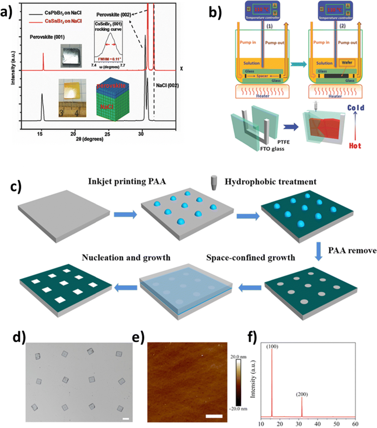 | ||
| Fig. 17 (a) Structural and morphological characterization studies of VPE halide perovskites on NaCl. θ–2θ XRD analysis of CsSnBr3/NaCl (red) and CsPbBr3/NaCl (black). Both samples show only (100) and higher order peaks parallel to NaCl(002). The left two insets show the camera images of the mirror-like 1 cm × 1 cm film obtained after growth. The right inset shows a (001) rocking curve for CsSnBr3 with a FWHM of 0.11°. Adapted with permission from ref. 292. (b) Schematic illustration of the space-confined method. Two flat glass slides are separated with two spacers to form a microreactor (top) and schematic diagram of the module to grow laminar CH3NH3PbBr3 crystal films, whose thickness was defined by polytetrafluoroethylene (PTFE) thin membranes’ thickness (bottom). Adapted with permission from ref. 294 and 296. Space-confined growth process of MAPbCl3 single-crystal arrays. (c) Schematic illustration of the fabrication process of MAPbCl3 single-crystal arrays. (d) Optical micrograph of the MAPbCl3 single-crystal arrays. The scale bar is 50 μm. (e) AFM image of the MAPbCl3 single crystal. The scale bar is 3 μm. (f) XRD pattern of the MAPbCl3 single-crystal arrays. Adapted with permission from ref. 295. | ||
Zhao et al. tried to grow a micrometer thick SCTF in the range of 3–10 μm on FTO/TiO2 substrates, but obtained an irregular shape of MAPbI3, because of the slow ion diffusion in the confined space.298 Chen et al. developed a hydrophobic interface confined lateral crystal growth method, where they did grow MAPbI3 SCTFs with controlled thicknesses of tens of micrometers, on HTL substrates.300 When the film thickness was increased from 500 nm to 200 μm, they reported the expansion of the absorbance to the near-IR region. Huang et al. were the first to report the growth of mixed-halide, mixed-cation (FAPbI3)0.85(MAPbBr3)0.15 SCTFs, where they made films with various thicknesses ranging from 10 to 50 μm, through the polydimethylsiloxane-assisted solvent evaporation method.301
Recently Li et al. synthesized a laminar MAPbBr3/MAPbBr3−xIx heterojunction with a thickness of about 11 μm with the space-limited inverse temperature crystallization growth method and a gaseous halide exchange process in sequence, which was a new approach for growing iodide-based perovskite SCTFs.302 In order to control the nucleation process, Gu et al. used a seed printing strategy, which was based on the space-confined approach, where they managed to create millimeter-sized MAPbBr3 SCTFs that resulted in high yields, under controlled thickness. With the printing process, the SCTFs can be transferred to most arbitrary substrates and to scalable fabrication of photodetectors and image sensors.303 More recently, a variety of perovskite single crystal arrays, such as MAPbBr3, CsPbCl3, CsPbBr3, Cs3Cu2I5, Cs3Bi2I9, and (BA)2(MA)3Pb4I11, were grown on Au electrodes using an inkjet-printed hydrophilic–hydrophobic substrate in the crystallization system to successfully fabricate high performance UV photodetectors.306Fig. 17c–f presents the schematic illustration of the space-confined growth procedure of MAPbCl3 SC arrays, along with morphological and crystallinity characterization results.
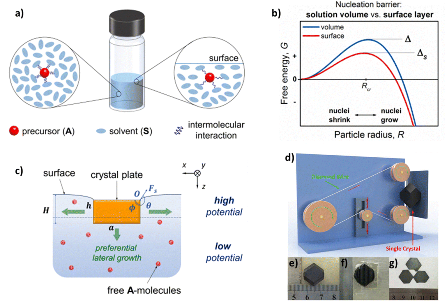 | ||
| Fig. 18 (a) Schematic of change in molecular interaction energies in the volume (left) and the surface layer (right) of the solution. Due to the surface tension effect, the intermolecular distances in the surface layer are increased, hence decreasing the corresponding interaction energy. (b) Graph illustrating the lower nucleation barrier for the solution surface layer compared to that in the solution volume. (c) Schematic of crystal growth during ITC. The free precursor molecules in the surface layer (above the dashed line) are mainly attached to the sides of the nucleus (due to the higher free energy gain), resulting in lateral growth of the crystal plate. The crystal plate is kept afloat by the solution surface tension. Adapted with permission from ref. 304. (d) The schematic illustration of the single-crystalline FAPbI3 wafer slicing process. (e) A FAPbI3 single crystal. (f) The single-crystalline FAPbI3 wafers sliced at the parallelogram natural crystallographic facets of a single-crystalline FAPbI3, cross-sectional view. (g) The single-crystalline FAPbI3 wafers, panoramic view. Adapted with permission from ref. 307. | ||
| Method | Perovskite | J SC (mA cm−2) | V OC (V) | FF | PCE (%) | Ref. |
|---|---|---|---|---|---|---|
| Droplet-pinned crystallization | MAPbI3 | 8.7 | 0.52 | 0.38 | 1.73 | 255 |
| ITC | FA0.6MA0.4PbI3 | 26.2 | 1.1 | 0.79 | 22.8 | 270 |
| AVC | (NH4)3Sb2IxBr9−x | 1.15 | 1.03 | 0.4288 | 0.51 | 283 |
| Space-confined method | MAPbBr3 | 8.77 | 1.31 | 0.62 | 7.11 | 297 |
| Space-confined method | MAPbI3 | 22.28 | 0.67 | 0.59 | 8.78 | 299 |
| Space-confined method | MAPbI3 | 20.5 | 1.06 | 0.741 | 16.1 | 300 |
| Space-confined method | (FAPbI3)0.85(MAPbBr3)0.15 | 23.14 | 1.03 | 0.51 | 12.18 | 301 |
| Space-confined method | MAPbI3 | 5.06 | 0.66 | 0.44 | 5.9 | 304 |
Liu et al. modified the surface tension assisted growth method, with the introduction of a driving force by solvent evaporation.305 They managed to grow within 30 min MAPbI3 SCTFs with a lateral size of centimeters and a thickness of tens of micrometers. With this modified method, it is possible to grow SCTF crystals with a higher quality, confirmed by the long charge recombination lifetime, as measured with TRPL. In a recent work, wafer-sized 2D BA2PbBr4 SCTFs were grown through a gas–liquid interface crystalline route, where the crystal formed along the side parallel to the solution. Consequently, the prepared thin film buoyed on the solution surface, due to the solution surface tension.306
5. Synthetic methods for 2D perovskites
The fundamental characteristics and device applications of 2D perovskites depend a lot on how they are synthesized in a controlled manner. Up to this point, several types of ultra-thin perovskites have been synthesized by utilizing various methods. In this section we will describe the current developments in the synthesis of 2D perovskites.5.1 Inorganic 2D perovskites
The colloidal synthesis method is one of the most used approaches for producing 2D inorganic halide perovskites.310–313Fig. 19 shows the structural analysis of the CsPbBr3 nanoplatelets formed through solution synthesis. While nanoplatelets might be produced at comparatively lower temperatures, reactions carried out above 150 °C would mostly result in nanocubes. At 130 °C, for example, nanoplatelets with lateral dimensions of 20 nm and a thickness of around 3 nm can be produced. CsPbI3 and CsPbCl3 nanoplatelets may be generated using anion exchange, and for device applications, they can be deposited onto substrates using the centrifugal casting process.311 The lateral size, however, is only around 20–300 nm, which is small for the assessment of the basic characteristics of a single nanosheet and the manufacture of devices. By dissolving Cs-oleate in oleic acid and adding short ligands, Shamsi et al. discovered that they could create CsPbBr3 ultra-thin rectangular shaped sheets of 3 nm and lateral dimensions ranging from 300 nm to 5 μm.312 High-quality 2D CsPbI3 perovskite nanosheets were produced by the space-confined vapor deposition approach by Zhai et al. By altering the growth temperature and distance, the 2D CsPbI3 perovskite's shape and crystal quality may be easily regulated. 2D CsPbI3 nanosheets are uniformly square-shaped and have a thickness of 6 nm and a side length of 10 μm, while the photoluminescence emission characteristics show a clear reliance on the 2D CsPbI3 nanosheets’ thickness.313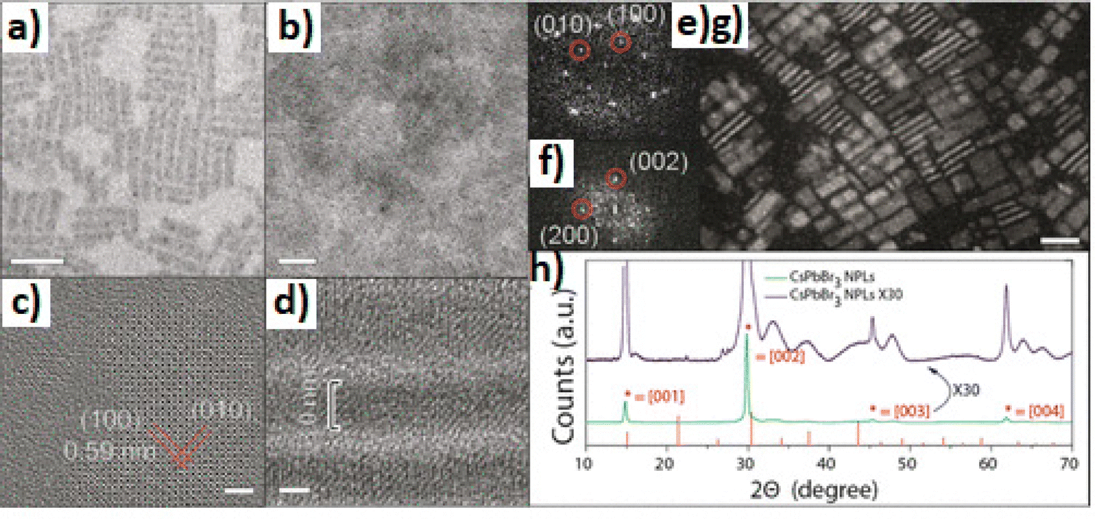 | ||
| Fig. 19 Structural analysis of CsPbBr3 NPLs emitting at 460 nm. TEM images of CsPbBr3 NPLs at (a) low concentrations and (b) high concentrations. HRTEM images of NPLs (c) in top view and (d) in stacks as well as their respective Fourier transform patterns (e and f). (g) STEM dark-field image of NPLs. (h) XRD patterns of CsPbBr3 NPLs. Reference pattern of cubic CsPbBr3, ICSD 29073. Scale bars correspond to 50 nm in (a) and (b), 2 nm in (c) and (d), and 20 nm in (g). Adapted with permission from ref. 310. | ||
Cs2PbCl2I2 nanosheets doped with Mn2+ were synthesized by Li et al. and Dutta et al. by an acid solution-assisted method resulting in all-inorganic 2D perovskites with ordered mixed halides.314,315 They showed that an efficient method to improve the photoluminescence characteristics of Cs2PbCl2I2 nanocrystals is to introduce appropriate Mn2+ together with Pb2+ into the crystals, which resulted in a higher PLQY of 16%. Note that the 2D CsPbX3 nanoplatelets correspond to the morphological structure of the perovskite, while the Cs2PbCl2I2 nanosheets are attributed to the molecular level.
A variety of inorganic lead perovskites can also be synthesized using CVD. Mica was used as the substrate by Zhang et al., who employed the van der Waals epitaxial CVD technique for the fabrication of CsPbX3 nanoplatelets.316 The perovskite nanoplatelets were relatively thick, ranging in thicknesses from 50 to 300 nm, although having fairly considerable lateral dimensions in the range of 1–20 μm. Some studies have conclusively shown that all-inorganic 2D perovskites of cesium lead halides have comparatively poor mobility, which is mostly due to the extremely low frequency of the Pb-I vibrations. This finding suggests that combined Pb/Sn- or Sn-based perovskites with the light components of Cl or Br should be viewed as better materials.317,318
5.2 Solution synthesis of 2D perovskites
The majority of 2D halide perovskites are created using hydrohalic acid solution synthesis, while multilayered 2D perovskites can be fabricated using this technique very effectively.319–322 Serving both as a solvent and as a halide source, hydrohalic acid must be compatible with the type of halide in the target perovskite. Under heating and stirring, the metal source, spacer (or spacer salt), and A-site cation salt dissolve, resulting in the ionization of all three components. To produce the desired crystal, the desired solution must be cooled to room temperature after it becomes clear. The perovskite with the same halide will be produced regardless of the anions in the metal source and cation salts because there is a significant excess of halide in the solution. The general rule is that substances with higher organic content are less soluble and will crystallize more quickly than substances with higher solubility. The solubility of the n = 1 compound determines the ratio of the spacer and Pb sources, which can be used to adjust the layer-number.323 Iodide perovskites can occasionally produce a light-yellow hydrate phase instead of the desired perovskite phase if the hot solution is quickly cooled to room temperature. This step-cooling technique can be used in some circumstances to obtain the 2D phase. The solution can be heated to 125 °C, which is just below the boiling point of HI, so that it is hot and the light-yellow phase can continue to be soluble after all of the initial ingredients have been dissolved under stirring and boiling. The desired 2D phase can still precipitate out because the solution is extremely concentrated. Iodide perovskites can act as crystal growth seeds once the first few crystals begin to precipitate out, while a second precipitation phase would not occur if the temperature were gradually lowered to room temperature (Fig. 20).324–326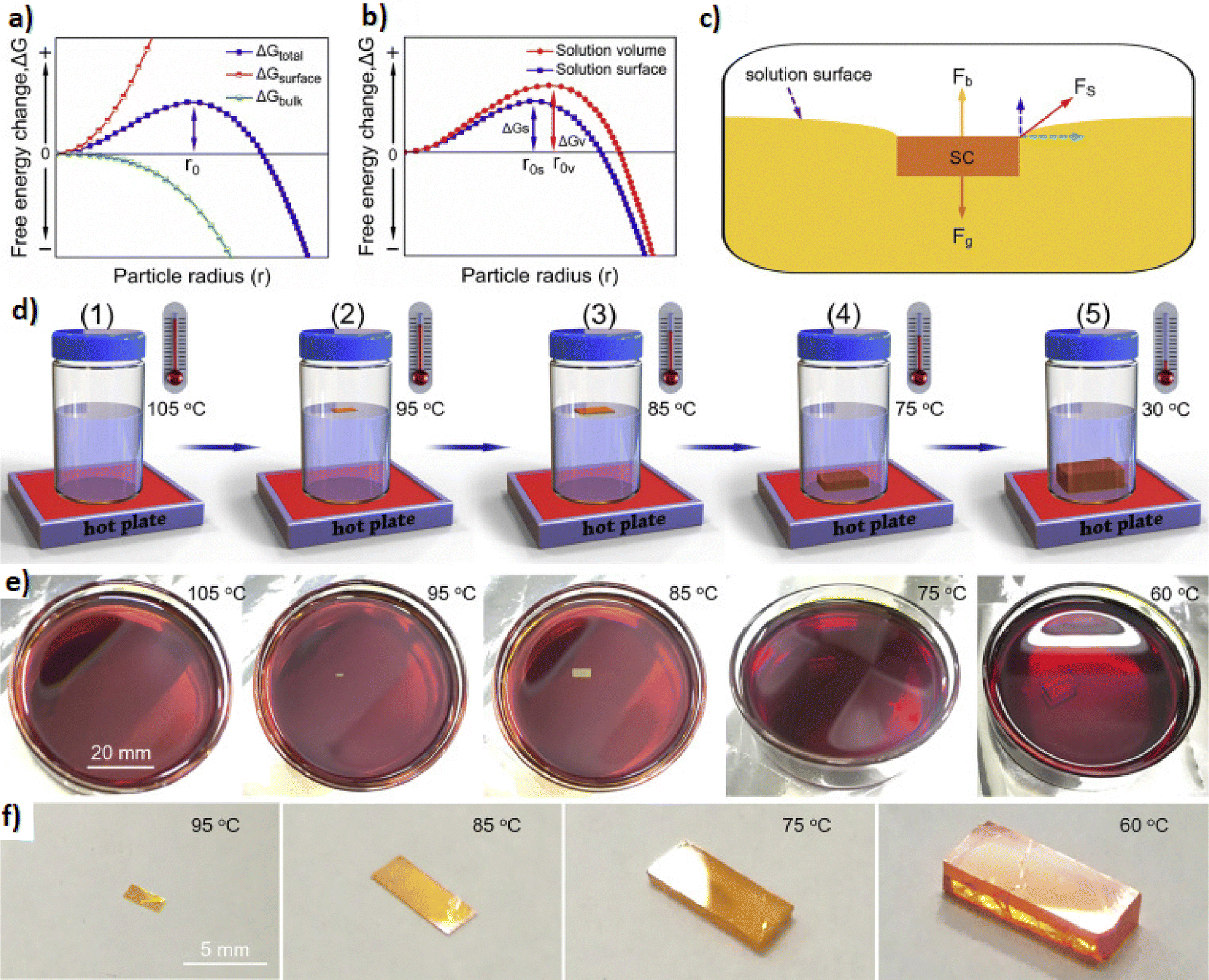 | ||
| Fig. 20 Crystallization of (PEA)2PbI4 PSCs. (a) The Gibbs free energy change ΔGtotal as a function of particle radius. ΔGtotal consists of a surface term ΔGs and a bulk term ΔGb. (b) Graph illustrating the lower nucleation barrier for the solution surface compared with that in the solution volume. (c) Schematic of the single crystal staying afloat on the solution surface. (d) Schematic of the surface tension-controlled crystallization process. (e) Photographs of the (PEA)2PbI4 PSCs grown at different temperatures. (f) Corresponding photographs of (PEA)2PbI4 PSCs completed at different temperatures. Adapted with permission from ref. 326. | ||
Organic solvents, including N,N-dimethylformamide (DMF), dimethyl sulfoxide (DMSO), and γ-butyrolactone (GBL), as well as mixtures of the aforementioned solvents, can also be used to create 2D halide perovskites.46,326 Most organic and inorganic salts can be dissolved using these polar solvents, and they may also work for cations that are insoluble in HI. Some 3D halide perovskites become less soluble in organic solvents as the temperature increases; as a result, the crystal can precipitate out when using this method, as it necessitates a thorough examination of each compound's solubility with temperature, which may differ from spacer to spacer.327 A large single crystal can also form by maintaining a constant solution temperature and allowing the solvent to slowly evaporate.328 Sometimes the decrease in solubility caused by a temperature change or solvent evaporation is insufficient to cause the crystal to precipitate. In these circumstances, the precipitation process can be sped up by gradually adding an antisolvent. A stoichiometric ratio of starting materials is dissolved in a small vial with a “good solvent,” much like solution synthesis using an organic solvent like DMF or DMSO. The vial with the cap open is then placed into a larger vial that contains a “poor solvent,” such as ethyl ether or dichloromethane, which serves as the antisolvent. The solubility of the perovskite phase decreases as the “poor solvent” gradually diffuses into the “good solvent,” and crystals may precipitate out.329–331
5.3 Substrate growth
Halide perovskites can be produced directly by the evaporation of their precursor solution on a substrate like silicon or glass in the form of atomically flat 2D sheets. On the substrate, the kinetics of crystal growth are significantly influenced by the rate of solvent evaporation. The 2D halide perovskite structures’ overall quality and thickness are consequently influenced by the polarity of the solvents used to dissolve the precursors, the solvent volume ratio, the crystallization temperature, and the make-up of the substrate surface.332–334By drop-casting the precursor solution onto a Si/SiO2 substrate at a moderate temperature, Yang and colleagues were able to showcase the growth of single-crystalline (BA)2PbBr4 perovskites. As a ternary co-solvent to dissolve the precursors, DMF–chlorobenzene–acetonitrile was used to regulate the thickness of the 2D perovskite sheets. Fast acetonitrile evaporation induces the formation and growth of ultrathin 2D perovskite sheets, whereas chlorobenzene decreases the solubility of halide perovskites in DMF and encourages crystallization.335
Another effective method for creating uniform, superior-quality films of 2D halide perovskites is spin-coating.333,336 Perovskite layers are typically deposited using this technique for the construction of devices like solar cells and LEDs. To create layered 2D halide perovskites, the precursors dissolved in DMF or DMSO are spin-coated on glass or ITO substrates in a single step or multiple steps, followed by ambient drying or annealing. In order to create perovskite solar cells, Smith et al. demonstrated the one-step spin coating of high-quality perovskite films.337 The SEM cross sectional image of the corresponding perovskite solar cell and the J–V characteristic curves are presented in Fig. 21a and b, respectively. The selective thickness of these 2D materials is largely determined by crystallization dynamics during the film growth in addition to the stoichiometric ratio of precursors and the size of organic cations.332 For instance, 2D halide perovskites made by quickly crystallizing stoichiometric precursors in DMF via spin coating and immediately annealing them at a high temperature do not always have stacking layers with a single value of n. They might include a variety of 2D layers with various n. On the other hand, Zhang et al. used a binary mixture of solvents as the precursors for perovskites.338 Toluene is a poor solvent that is known to cause the precipitation of perovskite crystals, whereas acetonitrile is a suitable solvent for the precursors. The controlled synthesis of 2D RP perovskites on substrates is made possible by the two solvents’ perfect miscibility in this situation, which could cause them to co-evaporate slowly at room temperature. As a result, nanosheets with various thicknesses were successfully produced.
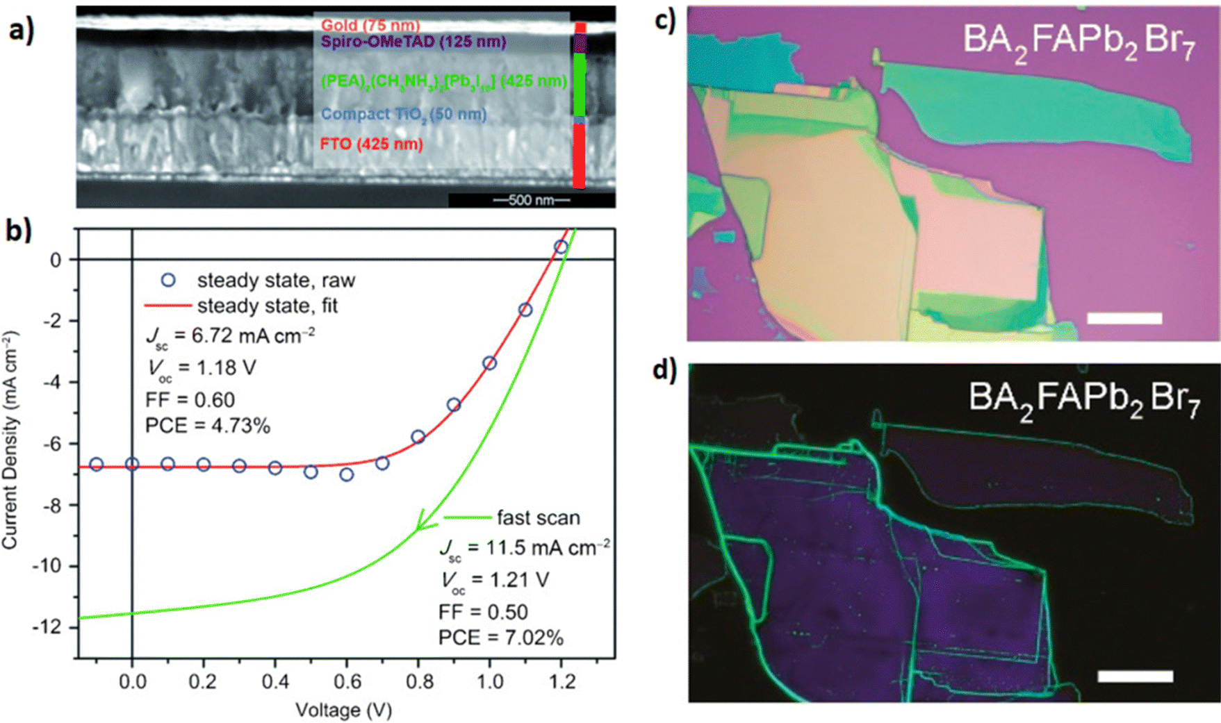 | ||
| Fig. 21 (a) SEM cross-sectional image and device configuration of planar devices utilizing (PEA)2(MA)2[Pb3I10] as the absorber layer. Scale bar = 500 nm. (b) Current–voltage (J–V) curves for the devices fabricated as given in (a). Adapted with permission from ref. 337. (c and d) Optical and PL images of a series of 2D BA2FAPb2Br7 lead halide perovskites mechanically exfoliated on SiO2/Si substrates. Adapted with permission from ref. 342. | ||
5.4 Exfoliation method
Since 2D RP perovskites have a van der Waals layered crystal structure, mechanical exfoliation can easily produce atomically thin layers of perovskites, just as it can with other conventional 2D materials like graphene.339 Niu et al. were able to produce from one to multiple layers of flakes by employing the micromechanical exfoliation technique.340 In order to study the fundamental properties of quasi-2D perovskites with various layer numbers, this synthesis method is ideally suited.341 However, due to the lack of size and thickness control over the obtained flakes, it cannot be widely used, and as a result, new techniques for creating atomically thin 2D RP perovskites were created.Another way to create 2D structures that are as thin as atoms is by repeatedly peeling a bulk perovskite crystal that has been adhered between the adhesive sides of two scotch tape strips.84,342
By applying pressure to a substrate with the scotch tape, the resulting 2D halide perovskite layers are transferred there. It is simple to create 2D halide perovskites using this method, but it is frequently challenging to precisely control the thickness of the inorganic layers; therefore the 2D halide perovskites made using the Scotch tape method are mechanically fragile, and their stability and photoluminescence quantum yield (PLQY) can be affected by the fractured surface (Fig. 21c and d). Yun et al. recently demonstrated ligand-assisted ball milling for mechanically exfoliating perovskite crystals to produce quasi-2D structures with improved PLQYs and stability.343
Furthermore, liquid exfoliation has been used to create 2D RP perovskites from 3D perovskites by incorporating the long chain molecules into the 3D perovskite structures. OlA was an oleylamine cation, and X was Cl, Br, or I when Hintermayr et al. reported the synthesis of OlA2MAn−1PbnX3n+1. MAPbX3 microcrystal powder was first dissolved in toluene with OlA and subjected to tip sonication during the procedure. The large particles were then centrifuged out, resulting in nanoplate dispersion.344 Exfoliating perovskite nanocrystals with a solvent or using sonication in the presence of many surface ligands results in colloidally stable ultrathin 2D halide perovskites.345 By diluting the colloidal nanocrystal solution, solvent-assisted exfoliation produces nanoplatelets of halide perovskites. The excess ligand molecules that are already present in or are later added penetrate the interlayer region and stabilize the newly formed surface as a result of the increase in osmotic swelling of nanocrystals caused by the solvent molecules at higher dilutions, which causes their fragmentation into nanoplatelets. Urban et al. showed that altering the level of dilution or ligand concentration caused perovskite nanocrystals to fragment into stable nanoplatelets of various thicknesses.346 Sonication is one external stimulus that can cause larger nanocrystals to break up into quasi-2D structures. Instead of diluting the nanocrystals, sonication in this case breaks them up into thin perovskite layers, allowing the organic ligands to pass through and interact with the newly formed facets, and then by centrifugation at various speeds, the 2D perovskite nanoplatelets with various thicknesses are separated.344
5.5 Grinding method
Solid-state grinding is a technique that can be used to completely eliminate solvent effects. For 3D halide perovskites, this is first accomplished by stoichiometrically grinding the raw materials in a mortar and pestle, then annealing the mixture to produce the desired phase. In particular, 2D perovskites that cannot be produced in solution, because the spacers are too soluble or insoluble, can be produced using this method.235,242,347 This method's advantage is that it can create 2D perovskites regardless of how soluble a spacer is. It is a good way to determine whether a spacer can create a 2D perovskite (if the solution synthesis does not work). This technique has not yet been used to synthesize 2D perovskites with more n > 3. Table 4 summarizes the electrical parameters of PSCs based on 2D perovskites.| Method | Perovskite | J SC (mA cm−2) | V OC (V) | FF | PCE (%) | Ref. |
|---|---|---|---|---|---|---|
| Solution synthesis | (CH3(CH2)2NH3)2(CH3NH3)5Pb6I19 | 16.30 | 1.05 | 0.7539 | 10.9 | 319 |
| Solution synthesis | (CH3(CH2)2NH3)2(CH3NH3)6Pb7I22 | 16.73 | 0.95 | 0.5603 | 8.93 | 319 |
| Solution synthesis | (CH3(CH2)2NH3)2(CH3NH3)8Pb9I28 | 21.84 | 0.801 | 0.7219 | 12.63 | 319 |
| Solution synthesis | (CH3(CH2)3NH3)2(CH3NH3)4Pb5I16 | 11.44 | 1.00 | 0.7559 | 8.71 | 320 |
| Solution synthesis | (ThMA)2FA4Pb5I16 | 23.39 | 1.075 | 0.758 | 19.06 | 324 |
| Solvent evaporation | (iso-BA)2(MA)4Pb5I16 | 18.1 | 1.15 | 0.772 | 16.0 | 332 |
| Spin-coating | BA2MA3Pb4I13 | 11.3 | 1.07 | 0.648 | 7.9 | 336 |
| Slow-solvent evaporation | (PEA)2(MA)2[Pb3I10] | 6.72 | 1.18 | 0.60 | 4.73 | 337 |
| Sonication | (CH3(CH2)3NH3)2(CH3NH3)3Sn4I13 | 24.1 | 0.229 | 0.457 | 2.53 | 347 |
6. Conclusions
In this review, we have summarized the synthetic approaches followed for the deposition of polycrystalline perovskite films and the growth of perovskite single crystals and their corresponding layers. The fabrication of high-quality perovskite layers has been recapitulated to be dependent on the synthetic method adopted. Various vacuum or solution based synthetic methods are effective and mature ways to fabricate high-quality polycrystalline films favorable for different applications. The carrier diffusion length, presence of defects, absorption coefficient and other optoelectronic properties are strongly related to the quality of the deposited film. Similarly, the growth of perovskite single crystals, 2D perovskites and the corresponding layers depends on the synthetic method applied and influences their effective material properties.All these methods can be manipulated in order to minimise perovskite destroying defects. The low stability of perovskite optoelectronics is attributed to the intrinsic low formation energy of the 3D perovskite lattice. This leads to defect formation (uncoordinated halide ions, cation vacancies), which can migrate through the perovskite and cause perovskite-destabilising redox reactions catalysed by water, oxygen, light, temperature or the applied electric field. Recently, the paramount importance of strain (mechanical deformation of the crystal lattice) in halide perovskites was highlighted since it can be tuned to improve the thermodynamic stability of perovskites or locally alter defect dynamics and charge transfer. By using suitable synthetic protocols combined with in situ strain engineering and/or chemical passivation approaches perovskite layers with improved properties can be obtained.
The potential of perovskites for creating higher efficiency optoelectronic devices has been unambiguously demonstrated. Halide perovskite materials offer excellent light absorption and charge-carrier mobilities, resulting in high device efficiencies with opportunities to realise a low-cost, industry-scalable technology. Achieving this potential requires that a suitable deposition method be followed for the fabrication of perovskite functional layers. A large variety of deposition methods have been already explored with great success in terms of device efficiency. However, they perhaps need to overcome barriers related to stability, environmental compatibility, and reproducibility. If the existing synthetic approaches can be modified in order for these concerns to be effectively addressed, perovskite-based technology holds transformational potential for rapid terawatt-scale solar deployment, efficient solid state lighting, field-effect transistor and memory applications and beyond.
Conflicts of interest
There are no conflicts to declare.References
- D. A. Egger, A. Bera, D. Cahen, G. Hodes, T. Kirchartz, L. Kronik, R. Lovrincic, A. M. Rappe, D. R. Reichman and O. Yaffe, Adv. Mater., 2018, 30, e1800691 CrossRef PubMed.
- J. Knutson, J. D. Martin and D. B. Mitzi, Inorg. Chem., 2005, 44, 4699–4705 CrossRef CAS PubMed.
- Y. Fang, Q. Dong, Y. Shao, Y. Yuan and J. Huang, Nat. Photonics, 2015, 9, 679–686 CrossRef CAS.
- M. A. Green, A. Ho-Baillie and H. J. Snaith, Nat. Photonics, 2014, 8, 506–514 CrossRef CAS.
- G. Xing, N. Mathews, S. Sun, S. S. Lim, Y. M. Lam, M. Grätzel, S. Mhaisalkar and T. C. Sum, Science, 2013, 342, 344–347 CrossRef CAS PubMed.
- M.-C. Tang, H. X. Dang, S. Lee, D. Barrit, R. Munir, K. Wang, R. Li, D.-M. Smilgies, S. De Wolf, D.-Y. Kim, T. D. Anthopoulos and A. Amassian, Solar RRL, 2021, 5, 2000718 CrossRef CAS.
- W. J. Yin, T. Shi and Y. Yan, Adv. Mater., 2014, 26, 4653–4658 CrossRef CAS PubMed.
- Q. Han, Y. Bai, J. Liu, K.-Z. Du, T. Li, D. Ji, Y. Zhou, C. Cao, D. Shin, J. Ding, A. D. Franklin, J. T. Glass, J. Hu, M. J. Therien, J. Liu and D. B. Mitzi, Energy Environ. Sci., 2017, 10, 2365–2371 RSC.
- Y. Zhai, K. Wang, F. Zhang, C. Xiao, A. H. Rose, K. Zhu and M. C. Beard, ACS Energy Lett., 2020, 5, 47–55 CrossRef CAS.
- A. Biewald, N. Giesbrecht, T. Bein, P. Docampo, A. Hartschuh and R. Ciesielski, ACS Appl. Mater. Interfaces, 2019, 11, 20838–20844 CrossRef CAS PubMed.
- S. D. Wolf, J. Holonsky, S.-J. Moon, P. Loper, B. Niesen, M. Ledinsky, F.-J. Haug, J.-H. Yum and C. Ballif, J. Phys. Chem. Lett., 2014, 5, 1035–1039 CrossRef PubMed.
- M. Delor, A. H. Slavney, N. R. Wolf, M. R. Filip, J. B. Neaton, H. I. Karunadasa and N. S. Ginsberg, ACS Energy Lett., 2020, 5, 1337–1345 CrossRef CAS.
- S. D. Stranks, G. E. Eperon, G. Grancini, C. Menelaou, M. J. P. Alcocer, T. Leijtens, L. M. Herz, A. Petrozza and H. J. Snaith, Science, 2013, 342, 341–344 CrossRef CAS PubMed.
- Q. Dong, Y. Fang, Y. Shao, P. Mulligan, J. Qiu, L. Cao and J. Huang, Science, 2015, 347, 967–970 CrossRef CAS PubMed.
- M. Saliba, T. Matsui, J. Y. Seo, K. Domanski, J. P. Correa-Baena, M. K. Nazeeruddin, S. M. Zakeeruddin, W. Tress, A. Abate, A. Hagfeldt and M. Grätzel, Energy Environ. Sci., 2016, 9, 1989–1997 RSC.
- M. Saliba, T. Matsui, K. Domanski, J.-Y. Seo, A. Ummadisingu, S. M. Zakeeruddin, J.-P. Correa-Baena, W. Tress, A. Abate, A. Hagfeldt and M. Grätzel, Science, 2016, 354, 206–209 CrossRef CAS PubMed.
- W. S. Yang, J. H. Noh, N. J. Jeon, Y. C. Kim, S. Ryu, J. Seo and S. I. Seok, Science, 2015, 348, 1234–1237 CrossRef CAS PubMed.
- S. S. Shin, E. J. Yeom, W. S. Yang, S. Hur, M. G. Kim, J. Im, J. Seo, J. H. Noh and S. I. Seok, Science, 2017, 356, 167–171 CrossRef CAS PubMed.
- M. Abdi-Jalebi, M. I. Dar, A. Sadhanala, S. P. Senanayak, M. Franckevičius, N. Arora, Y. Hu, M. K. Nazeeruddin, S. M. Zakeeruddin, M. Gratzel and R. H. Friend, Adv. Energy Mater., 2016, 6, 1502472 CrossRef.
- C. Bi, X. Zheng, B. Chen, H. Wei and J. Huang, ACS Energy Lett., 2017, 2, 1400–1406 CrossRef CAS.
- M. Era, S. Morimoto, T. Tsutsui and S. Saito, Appl. Phys. Lett., 1994, 65, 676–678 CrossRef CAS.
- T. Hattori, T. Taira, M. Era, T. Tsutsui and S. Saito, Chem. Phys. Lett., 1996, 254, 103–108 CrossRef CAS.
- K. Chondroudis and D. B. Mitzi, Chem. Mater., 1999, 11, 3028–3030 CrossRef CAS.
- H. Cho, S.-H. Jeong, M.-H. Park, Y.-H. Kim, C. Wolf, C.-L. Lee, J. H. Heo, A. Sadhanala, N. Myoung, S. Yoo, S. H. Im, R. H. Friend and T.-W. Lee, Science, 2015, 350, 1222–1225 CrossRef CAS PubMed.
- M. Yuan, L. N. Quan, R. Comin, G. Walters, R. Sabatini, O. Voznyy, S. Hoogland, Y. Zhao, E. M. Beauregard, P. Kanjanaboos, Z. Lu, D. H. Kim and E. H. Sargent, Nat. Nanotechnol., 2016, 11, 872–877 CrossRef CAS PubMed.
- C. R. Kagan, D. B. Mitzi and C. D. Dimitrakopoulos, Science, 1999, 286, 945–947 CrossRef CAS PubMed.
- D. B. Mitzi, C. D. Dimitrakopoulos and L. L. Kosbar, Chem. Mater., 2001, 13, 3728–3740 CrossRef CAS.
- D. B. Mitzi, C. D. Dimitrakopoulos, J. Rosner, D. R. Medeiros, Z. Xu and C. Noyan, Adv. Mater., 2002, 14, 1772–1776 CrossRef CAS.
- H. P. Kim, M. Vasilopoulou, H. Ullah, S. Bibi, A. E. X. Gavim, A. G. Macedo, W. J. da Silva, F. K. Schneider, A. A. Tahir, M. A. M. Teridi, P. Gao, A. R. B. M. Yusoff and M. K. Nazeeruddin, Nanoscale, 2020, 12, 7641–7650 RSC.
- K. Kang, W. Hu and X. Tang, J. Phys. Chem. Lett., 2021, 12, 11673–11682 CrossRef CAS PubMed.
- Y. Yao, Y. Peng, L. Li, X. Zhang, X. Liu, M. Hong and J. Luo, Angew. Chem., 2021, 60, 10598–10602 CrossRef CAS PubMed.
- Y. Zhang, S. Poddar, H. Hang, L. Gu, Q. Zhang, Y. Zhou, S. Yan, S. Zhang, Z. Song, B. Huang, G. Shen and Z. Fan, Sci. Adv., 2021, 7, eabg3788 CrossRef CAS PubMed.
- M. Vasilopoulou, B. S. Kim, H. P. Kim, W. J. da Silva, F. K. Schneider, M. A. M. Teridi, P. Gao, A. R. B. M. Yusoff and M. K. Nazeeruddin, Nano Lett., 2020, 20, 5081–5089 CrossRef CAS PubMed.
- T. Zhang, M. Yang, E. E. Benson, Z. Li, J. van de Lagemaat, J. M. Luther, Y. Yan, K. Zhu and Y. Zhao, Chem. Commun., 2015, 51, 7820–7823 RSC.
- O. Knop, R. E. Wasylishen, M. A. White, T. S. Cameron and M. J. V. Oort, Can. J. Chem., 1990, 68, 412–422 CrossRef CAS.
- W. J. Yin, Y. Yan and S. H. Wei, J. Phys. Chem. Lett., 2014, 5, 3625–3631 CrossRef CAS PubMed.
- Y. Fang, Q. Dong, Y. Shao, Y. Yuan and J. Huang, Nat. Photonics, 2015, 9, 679–686 CrossRef CAS.
- R. Babu, L. Giribabu and S. P. Singh, Cryst. Growth Des., 2018, 18, 2645–2664 CrossRef CAS.
- G. Maculan, A. D. Sheikh, A. L. Abdelhady, M. I. Saidaminov, M. A. Haque, B. Murali, E. Alarousu, O. F. Mohammed, T. Wu and O. M. Bakr, J. Phys. Chem. Lett., 2015, 6, 3781–3786 CrossRef CAS PubMed.
- M. Volmer and A. Weber, Phys. Chem., 1926, 119, 277–301 CAS.
- Z.-K. Tan, R. S. Moghaddam, M. L. Lai, P. Docampo, R. Higler, F. Deschler, M. Price, A. Sadhanala, L. M. Pazos, D. Credgington and F. Hanusch, Nat. Nanotechnol., 2014, 9, 687–692 CrossRef CAS PubMed.
- M. M. Lee, J. Teuscher, T. Miyasaka, T. N. Murakami and H. J. Snaith, Science, 2012, 338, 643–647 CrossRef CAS PubMed.
- J. Frenkel, J. Chem. Phys., 1939, 7, 538–547 CrossRef.
- L. Chen, Y.-Y. Tan, Z.-X. Chen, T. Wang, S. Hu, Z.-A. Nan, L.-Q. Xie, Y. Hui, J.-X. Huang, C. Zhan, S.-H. Wang, J.-Z. Zhou, J.-W. Yan, B.-W. Mao and Z.-Q. Tian, J. Am. Chem. Soc., 2019, 141, 1665–1671 CrossRef CAS PubMed.
- S. Kawachi, M. Atsumi, N. Saito, N. Ohashi, Y. Murakami and J.-I. Yamaura, J. Phys. Chem. Lett., 2019, 10, 6967–6972 CrossRef CAS PubMed.
- Y. Liu, Z. Yang, D. Cui, X. Ren, J. Sun, X. Liu, J. Zhang, Q. Wei, H. Fan, F. Yu, X. Zhang, C. Zhao and S. F. Liu, Adv. Mater., 2015, 27, 5176–5183 CrossRef CAS PubMed.
- J. M. Kadro, K. Nonomura, D. Gachet, M. Grätzel and A. Hagfeldt, Sci. Rep., 2015, 5, 11654 CrossRef PubMed.
- A. A. Zhumekenov, V. M. Burlakov, M. I. Saidaminov, A. Alofi, M. A. Haque, B. Turedi, B. Davaasuren, I. Dursun, N. Cho, A. M. El-Zohry, M. D. Bastiani, A. Giugni, B. Torre, E. Di Fabrizio, O. F. Mohammed, A. Rothenberger, T. Wu, A. Goriely and O. M. Bakr, ACS Energy Lett., 2017, 2, 1782–1788 CrossRef CAS.
- M. I. Saidaminov, A. L. Abdelhady, G. Maculan and O. M. Bakr, Chem. Commun., 2015, 51, 17658–17661 RSC.
- T. Baikie, Y. Fang, J. M. Kadro, M. Schreyer, F. Wei, S. G. Mhaisalkar, M. Graetzel and T. J. White, J. Mater. Chem. A, 2013, 1, 5628–5641 RSC.
- C. C. Stoumpos and M. G. Kanatzidis, Acc. Chem. Res., 2015, 48, 2791–2802 CrossRef CAS PubMed.
- X. Zhang, J.-X. Shen and C. G. Van de Walle, Adv. Energy Mater., 2020, 10, 1902830 CrossRef CAS.
- G. Kieslich, S. Sun and A. K. Cheetham, Chem. Sci., 2014, 5, 4712–4715 RSC.
- V. M. Goldschmidt, Naturwissenschaften, 1926, 14, 477–485 CrossRef CAS.
- Z. Li, M. Yang, J.-S. Park, S.-H. Wei, J. J. Berry and K. Zhu, Chem. Mater., 2016, 28, 284–292 CrossRef CAS.
- J.-W. Lee, S. Tan, S. I. L. Seok, Y. Yang and N. G. Park, Science, 2022, 375, 6583 CrossRef PubMed.
- B. Conings, J. Drijkoningen, N. Gauquelin, A. Babayigit, J. D'Haen, L. D'Olieslaeger, A. Ethirajan, J. Verbeeck, J. Manca, E. Mosconi, F. De Angelis and H.-G. Boyen, Adv. Energy Mater., 2015, 5, 1500477 CrossRef.
- X. Li, M. Ibrahim Dar, C. Yi, J. Luo, M. Tscumi, S. M. Zakeeruddin, M. K. Nazeeruddin, H. Han and M. Grätzel, Nat. Chem, 2015, 7, 703–711 CrossRef CAS PubMed.
- N. K. Kim, Y. H. Min, S. Noh, E. Cho, G. Jeong, M. Joo, S.-W. Ahn, J. S. Lee, S. Kim, K. ihm, H. Ahn, Y. Kang, H.-S. Lee and D. Kim, Sci. Rep., 2017, 7, 4645 CrossRef PubMed.
- G. E. Eperon, C. E. Beck and H. J. Snaith, Mater. Horiz., 2016, 3, 63 RSC.
- X. Zheng, C. Wu, S. K. Jha, Z. Li, K. Zhu and S. Priya, ACS Energy Lett., 2016, 1, 1014–1020 CrossRef CAS.
- N. Pellet, P. Gao, G. Gregori, T.-Y. Yang, M. K. Nazeeruddin, J. Maier and M. Grätzel, Angew. Chem., Int. Ed., 2014, 53, 3151–3221 CrossRef CAS PubMed.
- F. Brivio, C. Caetano and A. Walsh, J. Phys. Chem. Lett., 2016, 7, 1083–1087 CrossRef CAS PubMed.
- K. Tanaka, T. Takahashi, T. Ban, T. Kondo, K. Uchida and N. Miura, Solid State Commun., 2003, 127, 619–623 CrossRef CAS.
- Y. Cho, A. M. Soufiani, J. S. Yun, J. Kim, D. S. Lee, J. Seidel, X. Deng, M. A. Green, S. Huang and A. W. Y. Ho-Baillie, Adv. Energy Mater., 2018, 8, 1703392 CrossRef.
- N. Li, S. Tao, Y. Chen, X. Niu, C. K. Onwudinanti, C. Hu, Z. Qiu, Z. Xu, G. Zheng, L. Wang, Y. Zhang, L. Li, H. Liu, Y. Lun, J. Hong, X. Wang, Y. Liu, H. Xie, Y. Gao, Y. Bai, S. Yang, G. Brocks, Q. Chen and H. Zhou, Nat. Energy, 2019, 4, 408–415 CrossRef CAS.
- P. K. Nayak, D. T. Moore, B. Wenger, S. Nayak, A. A. Haghihgirad, A. Fineberg, N. K. Noel, O. G. Reid, G. Rumbles, P. Kukura, K. A. Vincent and H. J. Snaith, Nat. Commun., 2016, 7, 13303 CrossRef CAS PubMed.
- J. Jeong, M. Kim, J. Seo, H. Lu, P. Ahlawat, A. Mishra, Y. Yang, M. A. Hope, F. T. Eickemeyer, M. Kim, Y. J. Yoon, I. W. Choi, B. P. Darwich, S. J. Choi, Y. Jo, J. H. Lee, B. Walker, S. M. Zakeeruddin, L. Emsley, U. Rothlisberger, A. Hagfeldt, D. S. Kim, M. Grätzel and J. Y. Kim, Nature, 2021, 592, 381–385 CrossRef CAS PubMed.
- Y. Zhao, F. Ma, Z. Qu, S. Yu, T. Shen, H.-X. Deng, X. Peng, Y. Yuan, X. Zhang and J. You, Science, 2022, 377, 531–534 CrossRef CAS PubMed.
- Q. Jiang, J. Tong, Y. Xian, R. A. Kerner, S. P. Dunfield, C. Xiao, R. A. Scheidt, D. Kuciauskas, X. Wang, M. P. Hautzinger, R. Tirawat, M. C. Beard, D. P. Fenning, J. J. Berry, B. W. Larson, Y. Yan and K. Zhu, Nature, 2022, 611, 278–283 CrossRef CAS PubMed.
- R. Comin, G. Walters, E. S. Thibau, O. Voznyy, Z. H. Lu and E. H. Sargetnt, J. Mater. Chem. C, 2015, 3, 8839–8843 RSC.
- W.-J. Yin, T. Shi and Y. Yan, Appl. Phys. Lett., 2014, 104, 063903 CrossRef.
- H. Jin, E. Debroye, M. Keshavarz, I. G. Scheblykin, M. B. J. Roeffaers, J. Hofkens and J. A. Steele, Mater. Horiz., 2020, 7, 397–410 RSC.
- M. Rahil, R. M. Ansari, C. Prakash, S. S. Islam, A. Dixit and S. Ahmad, Sci. Rep., 2022, 12, 2176 CrossRef CAS PubMed.
- C.-H. Liao, M. A. Mahmud and A. W. Y. Ho-Baillie, Nanoscale, 2023, 15, 4219–4235 RSC.
- Y. Zheng, T. Niu, X. Ran, J. Qiu, B. Li, Y. Xia, Y. Chen and W. Huang, J. Mater. Chem. A, 2019, 7, 13860–13872 RSC.
- C. Lan, Z. Zhou, R. Wei and J. C. Ho, Mater. Today Energy, 2019, 11, 61–82 CrossRef CAS.
- G. Wu, R. Liang, Z. Zhang, M. Ge, G. Xing and G. Sun, Small, 2021, 17, 2103514 CrossRef CAS PubMed.
- S. Masi, A. F. Gualdron-Reyes and I. Mora-Sero, ACS Energy Lett., 2020, 5, 1974–1985 CrossRef CAS.
- X. Li, J. Hoffman, W. Ke, M. Chen, H. Tsai, W. Nie, A. D. Mohite, M. Kepenekian, C. Katan, J. Even, M. R. Wasielewski, C. C. Stoumpos and M. G. Kanatzidis, J. Am. Chem. Soc., 2018, 140, 12226–12238 CrossRef CAS PubMed.
- J. Cho, J. T. DuBose, A. N. T. Le and P. V. Kamat, ACS Mater. Lett., 2020, 2, 565–570 CrossRef CAS.
- D. H. Cao, C. C. Stoumpos, O. K. Fahra, J. T. Hupp and M. G. Kainatzidis, J. Am. Chem. Soc., 2015, 137, 7843–7850 CrossRef CAS PubMed.
- X. Gan, O. Wang, K. Liu, X. Du, L. Guo and H. Liu, Sol. Energy Mater. Sol. Cells, 2017, 162, 93–102 CrossRef CAS.
- N. Pandech, T. Kongnok, N. Palakawong, S. Limpijumnong, W. R. L. Lambrecht and S. Jungthawan, ACS Omega, 2020, 5, 25723–25732 CrossRef CAS PubMed.
- J. C. Blancon, H. Tsai, W. Nie, C. C. Stoumpos, L. Pedesseau, C. Katan, M. Kepenekian, C. M. Soe, K. Appavoo, M. Y. Sfeir, S. Tretiak, P. M. Ajayan, M. G. Kanatzidis, J. Even, J. J. Crochet and A. D. Mohite, Science, 2017, 355, 1288–1292 CrossRef CAS PubMed.
- C. C. Stoumpos, D. H. Cao, D. J. Clark, J. Young, J. M. Rondinelli, J. I. Jang, J. T. Hupp and M. G. Kanatzidis, Chem. Mater., 2016, 28, 2852–2867 CrossRef CAS.
- W. Li, X. Feng, K. Guo, W. Pan, M. Li, L. Liu, J. Song, Y. He and H. Wei, Adv. Mater., 2023, 2211808 CrossRef CAS PubMed.
- N. Parikh, M. M. Tavakoli, M. Pandey, A. Kalam, D. Prochowicz and P. Yadav, Sustainable Energy Fuels, 2021, 5, 1255–1279 RSC.
- W. Yang, X. Xiao, M. Li, J. Hu, X. Xiao, G. Tong, J. Chen and Y. He, Chem. Mater., 2021, 33, 4456–4464 CrossRef CAS.
- L. Li, X. Xu, L. Xiao, W. Jeng, J. Zhao, X. Kong and G. Zou, ACS Appl. Energy Mater., 2021, 4, 5935–5943 CrossRef CAS.
- J. Yan, W. Qiu, G. Wu, P. Heremans and H. Chen, J. Mater. Chem. A, 2018, 6, 11063–11077 RSC.
- T. Zhou, H. Ali, T. Liu, D. Lu, Z. Wan, X. Zhang, Y. Liu and Y. Chen, Adv. Mater., 2019, 31, 1901242–1901251 CrossRef PubMed.
- K. T. Cho, Y. Zhang, S. Orlandi, M. Cavazzini, I. Zimmermann, A. Lesch, N. Tabet, G. Pozzi, G. Grancini and M. K. Nazeeruddin, Nano Lett., 2018, 18, 5467–5474 CrossRef CAS PubMed.
- M. Liu, M. B. Johnston and H. J. Snaith, Nature, 2013, 501, 395–398 CrossRef CAS PubMed.
- S.-R. Bae, D. Y. Heo and S. Y. Kim, Mater. Today Adv., 2022, 14, 100232 CrossRef CAS.
- Y. Vaynzof, Adv. Energy Mater., 2020, 10, 2003073 CrossRef CAS.
- T. Abzieher, T. Feeney, F. Schackmar, Y. J. Donie, I. M. Hossain, J. A. Schwenzer, T. Hellmann, T. Mayer, M. Powalla and U. W. Paetzold, Adv. Funct. Mater., 2021, 31, 2104482 CrossRef CAS.
- P. Fan, D. Gu, G.-X. Liang, J.-T. Luo, J.-L. Chen, Z.-H. Zheng and D.-P. Zhang, Sci. Rep., 2016, 6, 29910 CrossRef CAS PubMed.
- O. Malinkwiewicz, A. Yella, Y. H. Lee, G. M. Espallargas, M. Graetzel, M. K. Nazeeruddin and H. J. Bolink, Nat. Photonics, 2014, 8, 128–132 CrossRef.
- J. Li, H. Wang, X. Y. Chin, H. A. Dewi, K. Vergeer, T. W. Goh, J. W. M. Lim, J. H. Lew, K. P. Loh, C. Soci, T. C. Sum, H. J. Bolink, N. Mathews, S. Mhaisalkar and A. Bruno, Joule, 2020, 4, 1035–1053 CrossRef CAS.
- X. Liu, X. Tan, Z. Liu, B. Sun, J. Li, S. Xi, T. Shi and G. Liao, J. Power Sources, 2019, 443, 227269 CrossRef CAS.
- C.-W. Chen, H.-W. Kang, S.-Y. Hsiao, P.-F. Yang, K.-M. Chiang and H.-W. Lin, Adv. Mater., 2014, 26, 6647–6652 CrossRef CAS PubMed.
- J. B. Patel, R. L. Milot, A. D. Wright, L. M. Herz and M. B. Johnston, J. Phys. Chem. Lett., 2016, 7, 96–102 CrossRef CAS PubMed.
- J. Feng, Y. Jiao, H. Wang, X. Zhu, Y. Sun, M. Du, Y. Du, Y. Cao, D. Yang and S. F. Liu, Energy Environ. Sci., 2021, 14, 3035–3043 RSC.
- H. M. Christen and G. Eres, J. Phys.: Condens. Matter, 2008, 20, 264005 CrossRef CAS PubMed.
- H. Schwarz and H. A. Tourtellotte, J. Vac. Sci. Technol., 1969, 6, 373–378 CrossRef CAS.
- U. Bansode, R. Naphade, O. Game, S. Agarkar and S. Ogale, J. Phys. Chem. C, 2015, 119, 9177–9185 CrossRef CAS.
- S. Hoffmann-Urlaub, Y. Zhang, Z. Wang, B. Kressdorf and T. Meyer, Appl. Phys. A: Mater. Sci. Process., 2020, 126, 553 CrossRef CAS.
- Y. Liang, Y. Yao, X. Zhang, W.-L. Hsu, Y. Gong, J. Shin, E. D. Wachsman, M. Dagenais and I. Takeuchi, AIP Adv., 2016, 6, 015001 CrossRef.
- P. Luo, S. Zhou, W. Xia, J. Cheng, C. Xu and Y. Lu, Adv. Mater. Interfaces, 2017, 4, 1600970 CrossRef.
- X. Chen, Y. Myung, A. Thind, Z. Gao, B. Yin, M. Shen, S. B. Cho, P. Cheng, B. Sadtler, R. Mishra and P. Banerjee, J. Mater. Chem. A, 2017, 5, 24728–24739 RSC.
- P. Luo, Z. Liu, W. Xia, C. Yuan, J. Cheng and Y. Lu, ACS Appl. Mater. Interfaces, 2015, 7, 2708–2714 CrossRef CAS PubMed.
- M. M. Tavakoli, L. Gu, Y. Gao, C. Reckmeier, J. He, A. L. Rogach, Y. Yao and Z. Fan, Sci. Rep., 2015, 5, 14083 CrossRef PubMed.
- M. Aaamir, M. Sher, M. D. Khan, M. A. Malik, J. Akhtar and N. Revaprasadu, Mater. Lett., 2017, 190, 244–247 CrossRef.
- D. S. Bhachu, D. O. Scanlon, E. J. Saban, H. Bronstein, I. P. Parklin, C. J. Carmalt and R. G. Palgrave, J. Mater. Chem. A, 2015, 3, 9071–9073 RSC.
- X. Liu, L. Cao, Z. Guo, Y. Li, W. Gao and L. Zhou, Materials, 2019, 12, 3304 CrossRef CAS PubMed.
- S. R. Ratnasingham, L. Mohan, M. Daboczi, T. Degousee, R. Bibions, O. Fenwick, J.-S. Kim, M. A. McLachlan and J. Briscoe, Mater. Adv., 2021, 2, 1606–1612 RSC.
- M. M. Tavakoli, S. M. Zakeeruddin, M. Grätzel and Z. Fan, Adv. Mater., 2018, 30, 1705998 CrossRef PubMed.
- S. Wang, L. K. Ono, M. R. Leyden, Y. Kato, S. R. Raga, M. V. Lee and Y. Qi, J. Mater. Chem. A, 2015, 3, 14631–14641 RSC.
- M. R. Leyden, L. K. Ono, S. R. Raga, Y. Kato, S. Wang and Y. Qi, J. Mater. Chem. A, 2014, 2, 18742–18745 RSC.
- Y. Peng, G. Jing and T. Cui, Mater. Res. Soc. Symp. Proc., 2015, 1771, 187–192 CrossRef.
- S. Ullah, L. Liu, S.-E. Yang, P. Liu, H. Guo and Y. Chen, J. Phys. D: Appl. Phys., 2022, 55, 064001 CrossRef CAS.
- P.-S. Shen, J.-S. Chen, Y.-H. Chiang, M.-H. Li, T.-F. Guo and P. Chen, Adv. Mater. Interfaces, 2016, 3, 1500849 CrossRef.
- L. Qiu, S. He, Y. Jiang, D.-Y. Son, L. K. Ono, Z. Liu, T. Kim, T. Bouloumis, S. Kazaoui and Y. Qi, J. Mater. Chem. A, 2019, 7, 6920–6929 RSC.
- H. S. Kim, C. R. Lee, J. H. Im, K.-B. Lee, T. Moehl, A. Marcioro, S.-J. Moon, R. Humphry-Baker, J.-H. Yum, J. E. Moser, M. Grätzel and N.-G. Park, Sci. Rep., 2012, 2, 591 CrossRef PubMed.
- J. Burschka, N. Pellet, S.-J. Moon, R. Humphry-Baker, P. Gao, M. K. Nazeeruddin and M. Grätzel, Nature, 2013, 499, 316–319 CrossRef CAS PubMed.
- K. Liang, D. B. Mitzi and M. T. Prikas, Chem. Mater., 1998, 10, 403–411 CrossRef CAS.
- K. L. Gardner, J. G. Tait, T. Merckx, W. Qiu, U. W. Paetzold, L. Kootstra, M. Jaysankar, J. Gehlhaar, D. Cheyns, P. Heremans and J. Poortmans, Adv. Energy Mater., 2016, 6, 1600386 CrossRef.
- L. Zheng, D. Zhang, Y. Ma, Z. Lu, Z. Chen, S. Wang, L. Xiao and Q. Gong, Dalton Trans., 2015, 44, 10582 RSC.
- P. J. Holliman, E. W. Jones, R. J. Hobbs, A. Connell, L. Furnell, R. Anthony and C. P. Kershaw, Mater. Lett., 2019, 2, 100011 CAS.
- W. Nie, H. Tsai, R. Asadpour, J.-C. Blancon, A. J. Neukirch, G. Gupta, J. J. Crochet, M. Chowalla, S. Tretiak, M. A. Alam, H.-L. Wang and A. D. Mohite, Science, 2015, 347, 522–525 CrossRef CAS PubMed.
- Q. Wang, W. Zhang, Z. Zhang, S. Liu, J. Wu, Y. Guan, A. Mei, Y. Rong, Y. Hu and H. Han, Adv. Energy Mater., 2020, 10, 1903092 CrossRef CAS.
- C. Li, Q. Guo, W. Qiao, Q. Chen, S. Ma, X. Pan, F. Wang, J. Yao, C. Zhang, M. Xiao, S. Dai and Z. Tan, Org. Electron., 2016, 33, 194–200 CrossRef CAS.
- M. Xiao, F. Huang, W. Huang, Y. Dkhissi, Y. Zhu, J. Etheridge, A. Gray-Weale, U. Bach, Y.-B. Cheng and L. Spiccia, Angew. Chem., Int. Ed., 2014, 53, 1–7 CrossRef.
- J.-H. Im, H.-S. Kim and N.-G. Park, APL Mater., 2014, 2, 081510 CrossRef.
- Z. Xiao, C. Bi, Y. Shao, Q. Dong, Q. Wang, Y. Yuan, C. Wang, Y. Gao and J. Huang, Energy Environ. Sci., 2014, 7, 2619–2623 RSC.
- Z. Yang, S. Zhang, L. Li and W. Chen, J. Materiomics, 2017, 3, 231–244 CrossRef.
- A. Kumar, M. Shkir, H. H. Somaily, K. L. Singh, B. C. Choudhary and S. K. Tripathi, Phys. B, 2022, 630, 413678 CrossRef CAS.
- C. Zuo and L. Ding, Angew. Chem., 2021, 60, 11242–11246 CrossRef CAS PubMed.
- Z. Lai, Y. Meng, F. Wang, X. Bu, W. Wang, P. Xie, W. Wang, C. Liu, S. Yip and J. C. Ho, Nano Res., 2022, 15, 3621–3627 CrossRef CAS.
- A. Mei, X. Li, L. Liu, Z. Ku, T. Liu, Y. Rong, M. Xu, M. Hu, J. Chen, Y. Yang, M. Grätzel and H. Han, Science, 2014, 345, 295–298 CrossRef CAS PubMed.
- X. Li, M. Tschumi, H. Han, S. S. Babkair, R. A. Alzubaydi, A. A. Ansari, S. S. Habib, M. K. Nazeeruddin, S. M. Zakeeruddin and M. Grätzel, Energy Technol., 2015, 3, 551–555 CrossRef CAS.
- C. Zuo, A. D. Scully and M. Gao, ACS Appl. Mater. Interfaces, 2021, 13, 56217–56225 CrossRef CAS PubMed.
- S. D. Stranks, P. K. Nayak, W. Zhang, T. Stergiopoulos and H. J. Snaith, Angew. Chem., Int. Ed., 2015, 54, 3240–3248 CrossRef CAS PubMed.
- T.-B. Song, Q. Chen, H. Zhou, C. Jiang, H.-H. Wang, Y. M. Yang, Y. Liu, J. You and Y. Yang, J. Mater. Chem. A, 2015, 3, 9032–9050 RSC.
- H. Zhou, Q. Chen and Y. Yang, MRS Bull., 2015, 40, 667–673 CrossRef CAS.
- Q. Chen, H. Zhou, Z. Hong, S. Luo, H.-S. Duan, H.-H. Wang, Y. Liu, G. Li and Y. Yang, J. Am. Chem. Soc., 2014, 136, 622–625 CrossRef CAS PubMed.
- R. Sedighi, F. Tajabadi, S. Shahbazi, S. Gholipour and N. Taghavinia, ChemPhysChem, 2016, 17, 2382–2388 CrossRef CAS PubMed.
- W.-W. Zuo, Y.-G. Yang, W.-F. Fu, M. Li, M. M. Byranvand, D. D. Girolamo, J. Pascual, M.-Q. Li, L.-N. Li, A. Abate, M. Saliba and Z.-K. Wang, ACS Mater. Lett., 2022, 4, 448–456 CrossRef CAS.
- J. Chen, J. Xu, L. Xiao, B. Zhang, S. Dai and J. Yao, ACS Appl. Mater. Interfaces, 2017, 9, 2449–2458 CrossRef CAS PubMed.
- Y.-A. Chen, H.-W. Shiu, Y.-J. Hsu, L. E. Mundt, W.-T. Hung, T. Ohigashi, M.-H. Li and P. Chen, J. Phys. Chem. C, 2021, 125, 26601–26612 CrossRef CAS.
- M. U. Ali, W. Cai, J. Cai, J. Miao, S. Zhang, J. Chen, L. Xiao, H. Meng, C. Yan and G. Wei, Adv. Opt. Mater., 2022, 10, 2100671 CrossRef CAS.
- M. S. Shadabroo, H. Abdizadeh and M. R. Golobostanfard, ACS Appl. Energy Mater., 2021, 4, 6797–6805 CrossRef CAS.
- M. Prakasam, O. Viraphong, O. Cambon and A. Largeteau, Hydrothermal Crystal Growth and Applications, in Advances in Solid Oxide Fuel Cells and Electronic Ceramics, ed. N. P. Bansal, M. Kusnezoff and K. Shimamura, John Wiley & Sons, Inc., 2015, ch. 15, pp. 151–156 Search PubMed.
- R. C. M. Mambote, M. A. Reuter, P. Krijgsman and R. D. Schuiling, Miner. Eng., 2000, 13, 803–822 CrossRef CAS.
- S.-H. Feng and G.-H. Li, Hydrothermal and Solvothermal Syntheses, in Modern Inorganic Synthetic Chemistry, ed. R. Xu and Y. Xu, Elsevier B.V., 2017, ch. 4, pp. 73–104 Search PubMed.
- K. Byrappa and M. Yoshimura, 10-Hydrothermal technology for nanotechnology – A technology for processing of advanced materials, Handbook of hydrothermal technology, William Andrew Publishing, 2nd edn, 2013, pp. 615–762 Search PubMed.
- Y. X. Gan, A. H. Jayatissa, Z. Yu, X. Chen and M. Li, J. Nanomater., 2020, 2020, 8917013 Search PubMed.
- J. C. Rendón-Angeles, Z. Matamoros-Veloza, K. L. Montoya-Cisneros, J. L. Cuevas and K. Yanagisawa, Synthesis of perovskite oxides by hydrothermal processing – From thermodynamic modelling to practical processing approaches, perovskite materials – synthesis, in Characterisation, Properties, and Applications, ed. L. Pan and G. Zhu, IntechOpen, 2016 Search PubMed.
- H.-R. Xia, W.-T. Sun and L.-M. Peng, Chem. Commun., 2015, 51, 13787–13790 RSC.
- K. Mahmood, A. Khalid and M. T. Mehran, Nanoscale Adv., 2019, 1, 64–70 RSC.
- G. Murugadoss, R. Thangamuthu, S. M. S. Kumar, N. Anandhan, M. R. Kumar and A. Rathishkumar, J. Alloys Compd., 2019, 787, 17–26 CrossRef CAS.
- M. Jansen, Angew. Chem., Int. Ed., 2002, 41, 3746–3766 CrossRef CAS PubMed.
- R. I. Walton, Chem. Soc. Rev., 2002, 31, 230–238 RSC.
- Y. Sun and H.-C. Zhou, Sci. Technol. Adv. Mater., 2015, 16, 054202 CrossRef PubMed.
- R. A. Laudise, Chem. Eng. News, 1987, 65, 30–43 CrossRef CAS.
- C. S. Cundy and P. A. Cox, Chem. Rev., 2003, 103, 663–702 CrossRef CAS PubMed.
- D. R. Modeshia and R. I. Walton, Chem. Soc. Rev., 2010, 39, 4303–4325 RSC.
- C. N. R. Rao and J. Gopalakrishnan, Acc. Chem. Res., 1987, 20, 228–235 CrossRef CAS.
- C. N. R. Rao, J. Mater. Chem. A, 1999, 9, 1–14 RSC.
- B. Zhang, F. Guo, L. Yang, X. Jia, B. Liu, Z. Xie, D. Chen, H. Lu, R. Zhang and Y. Zheng, J. Cryst. Growth, 2017, 459, 167–172 CrossRef CAS.
- F. Guo, B. Zhang, J. Wang, H. Ba, R. Guo, Y. Huang and P. Ren, Opt. Mater. Express, 2017, 7, 4156–4162 CrossRef CAS.
- Y. Chen, S. Yang, X. Chen, Y. C. Zheng, Y. Hou, Y. H. Li, H. D. Zeng and H. G. Yang, J. Mater. Chem. A, 2015, 3, 15854–15857 RSC.
- W. Zhai, J. Lin, Q. Li, K. Zheng, Y. Huang, Y. Yao, X. He, L. Li, C. Yu, C. Liu, Y. Fang, Z. Liu and C. Tang, Chem. Mater., 2018, 30, 3714–3721 CrossRef CAS.
- D. Chen, G. Fang, X. Chen, L. Lei, J. Zhong, Q. Mao, S. Zhou and J. Li, J. Mater. Chem. C, 2018, 6, 8990–8998 RSC.
- C. Liu, J. Lin, W. Zhai, Z. Wen, X. He, M. Yu, Y. Huang, Z. Guo, C. Yu and C. Tang, RSC Adv., 2019, 9, 39315–39322 RSC.
- W. Zhai, J. Lin, C. Li, S. Hu, Y. Huang, C. Yu, Z. Wen, Z. Liu, Y. Fang and C. Tang, Nanoscale, 2018, 10, 21451–21458 RSC.
- Z. Peng, D. Yang, B. Yin, X. Guo, S. Li, Q. Zhan, X. Xiao, X. Liu, Z. Xia, Z. Yang, J. Qiu and G. Dong, Sci, China Mater., 2021, 64, 2261–2271 CrossRef CAS.
- M. Yu, D. Zhang, Y. Xu, J. Lin, C. Yu, Y. Fang, Z. Liu, Z. Guo, C. Tang and Y. Huang, J. Colloid Interface Sci., 2022, 608, 2367–2376 CrossRef CAS PubMed.
- N. N. Gharat and V. K. Rathod, Ultrasound-assisted organic synthesis, Green Sustainable Process for Chemical and Environmental Engineering and Science Sonochemical Organic Synthesis, Elsevier, 2020, ch. 1, 1–41 Search PubMed.
- J. J. Hinman and K. S. Suslick, Top. Curr. Chem., 2017, 375, 12 CrossRef PubMed.
- V. R. Raja, D. R. Rosaline, A. Suganthia and M. Rajarajan, Ultrason. Sonochem., 2018, 44, 73–85 CrossRef PubMed.
- Y. Zhang, M. Park, H. Y. Kim, B. Ding and S.-J. Park, Sci. Rep., 2017, 7, 45086 CrossRef CAS PubMed.
- J. C. Colmenares, E. Kuna and P. Lisowski, Top. Curr. Chem., 2016, 374, 59 CrossRef PubMed.
- M. Ashokkumar, J. L. S. Kentish and F. Grieser, Ultrason. Sonochem., 2007, 14, 470–475 CrossRef CAS PubMed.
- D. M. Jang, D. H. Kim, K. Park, J. Park, J. W. Lee and J. K. Song, J. Mater. Chem. C, 2016, 4, 10625–10629 RSC.
- W. Peng, L. Wang, B. Murali, K.-T. Ho, A. Bera, N. Cho, C.-F. Kang, V. M. Burlakov, J. Pan, L. Sinatra, C. Ma, W. Xu, D. Shi, E. Alarousu, A. Goriely, J.-H. He, O. F. Mohammed, T. Wu and O. M. Bakr, Adv. Mater., 2016, 28, 3383–3390 CrossRef CAS PubMed.
- L.-C. Chen, Z.-L. Tseng, S. Y. Chen and S. Yang, Ceram. Int., 2017, 43, 16032–16035 CrossRef CAS.
- K. Umemoto, H. Ebe, R. Sato, J. Enomoto, N. Oshita, T. Kimura, T. Inose, T. Nakamura, T. Chiba, S. Asakura, H. Uji-I and A. Masuhara, ACS Sustainable Chem. Eng., 2020, 8, 16469–16476 CrossRef CAS.
- J. Enomoto, R. Sato, M. Yokoyama, T. Kimura, N. Oshita, K. Umemoto, S. Asakura and A. Masuhara, RSC Adv., 2022, 12, 5571–5576 RSC.
- A. Kokel, C. Schäfer and B. Torok, Microwave-Assisted Reactions in Green Chemistry, in Green Chemistry and Chemical Engineering. Encyclopedia of Sustainability Science and Technology Series, ed. B. Han and T. Wu, Springer, New York, 2019, pp. 537–612 Search PubMed.
- M. B. Gawande, S. N. Shelke, R. Zboril and R. S. Varma, Acc. Chem. Res., 2014, 47, 1338–1348 CrossRef CAS PubMed.
- A. Kumar, Y. Kuang, Z. Liang and X. Sun, Microwave chemistry, recent advancements, and eco-friendly microwave-assisted synthesis of nanoarchitectures and their applications: a review, Mater. Today Nano, 2020, 11, 100076 CrossRef.
- M. Henary, C. Kananda, L. Rotolo, B. Savino, E. A. Owens and G. Cravotto, RSC Adv., 2020, 10, 14170–14197 RSC.
- R. Gedye, F. Smith, K. Westaway, H. Ali and L. Baldisera, Tetrahedron Lett., 1986, 27, 279e282 CrossRef.
- R. J. Giguere, T. L. Bray, S. M. Duncan and G. J. Majetich, Tetrahedron Lett., 1986, 27, 4945e4948 CrossRef.
- A. Kojima, K. Teshima, Y. Shirai and T. Miyasaka, J. Am. Chem. Soc., 2009, 131, 6050–6051 CrossRef CAS PubMed.
- Q. Cao, S. Yang, Q. Gao, L. Lei, Y. Yu, J. Shao and Y. Liu, ACS Appl. Mater. Interfaces, 2016, 8, 7854–7861 CrossRef CAS PubMed.
- B. Yang, O. Dyck, J. Poplawsky, J. Keum, A. Puretzky, S. Das, I. Ivanov, C. Rouleau, G. Duscher, D. Geohegan and K. Xiao, J. Am. Chem. Soc., 2015, 137, 9210–9213 CrossRef CAS PubMed.
- M. Kim, G.-H. Kim, K. S. Oh, Y. Jo, H. Yoon, K.-H. Kim, H. Lee, J. Y. Kim and D. S. Kim, ACS Nano, 2017, 11, 6057–6064 CrossRef CAS PubMed.
- L. Huang, Z. Hu, J. Xu, K. Zhang, J. Zhang and Y. Zhu, Sol. Energy Mater. Sol. Cells, 2015, 141, 377–382 CrossRef CAS.
- X. Chen, Z. Wang, R.-J. Wu, H.-L. Cheng and H.-C. Chui, Photonics, 2021, 8, 30 CrossRef CAS.
- C.-H. Lin, Z. Lyu, Y. Zhuo, C. Zhao, J. Yang, C. Liu, J. Kim, T. He, L. Hu, F. Li, Y. Shen, K. Liu, W. Yu and T. Wu, Adv. Opt. Mater., 2020, 8, 2001740 CrossRef CAS.
- I. Bilecka and M. Niederberger, Nanoscale, 2010, 2, 1358–1374 RSC.
- H. Pan, X. Li, X. Zhang, J. Liu, X. Chen, H. Zhang, A. Huang and Z. Xiao, Langmuir, 2020, 36, 13663–13669 CrossRef CAS PubMed.
- H. Zhang, J. Mao, H. He, D. Zhang, H. L. Zhu, F. Xie, K. S. Wong, M. Grätzel and W. C. Choy, Adv. Energy Mater., 2015, 5, 1501354 CrossRef.
- Z. Yang, B. Cai, B. Zhou, T. Yao, W. Yu, S. F. Liu, W. H. Zhang and C. Li, Nano Energy, 2015, 15, 670–678 CrossRef CAS.
- B. A. Rosales, L. Men, S. D. Cady, M. P. Hanrahan, A. J. Rossini and J. Vela, Chem. Mater., 2016, 28, 6848–6859 CrossRef CAS.
- C. C. Hsu, S. M. Yu, K. M. Lee, C. J. Lin, H. C. Cheng and F. R. Chen, Sol. Energy Mater. Sol. Cells, 2021, 227, 111014 CrossRef CAS.
- L. Chen, F. Tang, Y. Wang, S. Gao, W. Cao, J. Cai and L. Chen, Nano Res., 2015, 8, 263–270 CrossRef CAS.
- H. Zheng, Y. Liu and J. Sun, Appl. Surface Sci., 2017, 405, 412–419 CrossRef CAS.
- H. Huang, A. S. Susha, S. V. Kershaw, T. F. Hung and A. L. Rogach, Adv. Sci., 2015, 2, 1500194 CrossRef PubMed.
- J. Sun, F. Li, J. Yuan and W. Ma, Small Methods, 2021, 5, 2100046 CrossRef CAS PubMed.
- S. Ghosh, S. Mishra and T. Singh, Adv. Mater. Interfaces, 2020, 7, 2000950 CrossRef CAS.
- W. Xu, Y. Gao, W. Ming, F. He, J. Li, X.-H. Zhu, F. Kang, J. Li and G. Wei, Adv. Mater., 2020, 32, 2003965 CrossRef CAS PubMed.
- D. S. Ahmed, B. K. Mohammed and M. K. A. Mohammed, J. Mater. Sci., 2021, 56, 15205–15214 CrossRef CAS.
- J. Li, X. Hua, F. Gao, X. Ren, C. Zhang, Y. Han, Y. Li, B. Shi and S. F. Liu, J. Energy Chem., 2022, 66, 1–8 CrossRef.
- S. Paek, P. Schouwink, E. N. Athanasopoulou, K. T. Cho, G. Grancini, Y. Lee, Y. Zhang, F. Stellacci, M. K. Nazeeruddin and P. Gao, Chem. Mater., 2017, 29, 3490–3498 CrossRef CAS.
- L. Chouhan, S. Ghimire, C. Subrahmanyam, T. Miyasaka and V. Biju, Chem. Soc. Rev., 2020, 49, 2869–2885 RSC.
- S. Ghimire, L. Chouhan, Y. Takano, K. Takahashi, T. Nakamura, K. I. Yuyama and V. Biju, ACS Energy Lett., 2018, 4, 133–141 CrossRef.
- L. C. Schmidt, A. Pertegás, S. González-Carrero, O. Malinkiewicz, S. Agouram, G. Minguez Espallargas, H. J. Bolink, R. E. Galian and J. Pérez-Prieto, J. Am. Chem. Soc., 2014, 136, 850–853 CrossRef CAS PubMed.
- S. Sun, D. Yuan, Y. Xu, A. Wang and Z. Deng, ACS Nano, 2016, 10, 3648–3657 CrossRef CAS PubMed.
- L. Potesescu, S. Yakunin, M. I. Bodnarchuk, F. Krieg, R. Caputo, C. H. Hendon, R. X. Yang, A. Walsh and M. V. Kovalenko, Nano Lett., 2015, 15, 3692–3696 CrossRef PubMed.
- L. Potesescu, S. Yakunin, M. I. Bodnarchuk, F. Bertolotti, N. Masciocchi, A. Guagliardi and M. V. Kovalenko, J. Am. Chem. Soc., 2016, 138, 14202–14205 CrossRef PubMed.
- F. Zhang, H. Zhong, C. Chen, X. G. Hu, H. Huang, J. Han, B. Zou and Y. Dong, ACS Nano, 2015, 9, 4533–4542 CrossRef CAS PubMed.
- A. J. Prochazkova, M. C. Scharber, C. Yumusak, J. Másilko, O. Brüggemann, M. Weiter, N. S. Sariciftci, J. Krajcovic, Y. Salinas and A. Kovalenko, Sci. Rep., 2020, 10, 1–12 CrossRef PubMed.
- J. Zhang, Y. Yang, H. Deng, U. Farooq, X. Yang, J. Khan, J. Tang and H. Song, ACS Nano, 2017, 11, 9294–9302 CrossRef CAS PubMed.
- H. Chen, Z. Wei, X. Zheng and S. Yang, Nano Energy, 2015, 15, 216–226 CrossRef CAS.
- J. A. Koza, J. C. Hill, A. C. Demster and J. A. Switzer, Chem. Mater., 2015, 28, 339–405 Search PubMed.
- G. Popov, M. Mattinen, M. L. Kemell, M. Ritala and M. Leskelä, ACS Omega, 2016, 1, 1296–1306 CrossRef CAS PubMed.
- J. Yadav, Q. Liang and S. Pan, J. Phys. Chem. C, 2020, 124, 10659–10668 CrossRef CAS.
- P. Luo, S. Zhou, Z. Liu, W. Xia, L. Sun, J. Cheng, C. Xu and Y. Lu, Chem. Commun., 2016, 52, 11203–11206 RSC.
- D. Liu, K. Liu, Y. Liu, J. Bai, M. Dai, F. Liu and G. Lu, Sol. Energy, 2020, 212, 275–281 CrossRef CAS.
- X. Wang, S. Abbasi, D. Zhang, J. Wang, Y. Wang, Z. Cheng, H. Liu and W. Shen, ACS Appl. Mater. Interfaces, 2020, 12, 50455–50463 CrossRef CAS PubMed.
- A. D. Jodlowski, A. Yépez, R. Luque, L. Camacho and G. de Miguel, Benign-by-design solventless mechanochemical of three-,two-, and one-dimensional hybrid perovskites, Angew. Chem., Int. Ed., 2016, 55, 14972 CrossRef CAS PubMed.
- P. Pal, S. Saha, A. Banik, A. Sarkar and K. Biswas, Chem. – Eur. J., 2018, 24, 1811 CrossRef CAS PubMed.
- N. Leupold, K. Schötz, S. Cacovich, I. Bauer, M. Schultz, M. Daubinger, L. Kaiser, A. Rebai, J. Rousset, A. Köhler, P. Schulz, R. Moos and F. Panzer, ACS Appl. Mater. Interfaces, 2019, 11, 30259 CrossRef CAS PubMed.
- A. Jana, M. Mittal, A. Singla and S. Sapra, Chem. Commun., 2017, 53, 3046 RSC.
- D. J. Kubicki, D. Prochowicz, A. Hofstetter, P. Péchy, S. M. Zakeeruddin, M. Grätzel and L. Emsley, J. Am. Chem. Soc., 2017, 139, 10055 CrossRef CAS PubMed.
- A. M. Askar, A. Karmakar, G. M. Bernard, M. Ha, V. V. Terskikh, B. D. Wiltshire, S. Patel, J. Fleet, K. Shankar and V. K. Michaelis, J. Phys. Chem. Lett., 2018, 9, 2671 CrossRef CAS PubMed.
- L. Protesescu, S. Yakunin, O. Nazarenko, D. N. Dirin and M. V. Kovalenko, ACS Appl. Nano Mater., 2018, 1, 1300 CrossRef CAS PubMed.
- A. Karmakar, M. S. Dodd, X. Zhang, M. S. Oakley, M. Klobukowski and V. K. Michaelis, Chem. Commun., 2019, 55, 5079 RSC.
- F. Palazon, Y. E. L. Ajjouri, P. Sebastia-Luna, S. Lauciello, L. Manna and H. J. Bolink, J. Mater. Chem. C, 2019, 7, 11406 RSC.
- C. A. López, C. Abia, M. C. Alvarez-Galván, B.-K. Hong, M. V. Martínez-Huerta, F. Serrano-Sánchez, F. Carrascoso, A. Castellanos-Gómez, M. T. Fernández-Díaz and J. A. Alonso, ACS Omega, 2020, 5, 5931 CrossRef PubMed.
- A. Goyal, E. Andrioti, Y. Tang, Q. Zhao, K. Zheng, K. D. Newell and P. Schall, J. Phys. Mater., 2022, 5, 024005 CrossRef.
- Y. E. L. Ajjouri, F. Locardi, M. C. Gélvez-Rueda, M. Prato, M. Sessolo, M. Ferretti, F. C. Grozema, F. Palazon and H. J. Bolink, Energy Technol., 2020, 8, 1900788 CrossRef.
- K. Kundu, P. Dutta, P. Acharyya and K. Biswas, Mater. Res. Bull., 2021, 140, 111339 CrossRef CAS.
- K. Kundu, P. Dutta, P. Acharyya and K. Biswas, J. Phys. Chem. C, 2021, 125, 4720–4729 CrossRef CAS.
- P. Sebastian-Luna, J. Calbo, N. Albiach-Sebastian, M. Sessolo, F. Palazon, E. Orti and H. J. Bolink, Chem. Mater., 2021, 33, 8028–8035 CrossRef.
- D. Prochowicz, P. Yadav, M. Saliba, D. J. Kubicki, M. M. Tavakoli, S. M. Zakeeruddin, J. Lewiński, L. Emsley and M. Grätzel, Nano Energy, 2018, 49, 523 CrossRef CAS.
- B. Dou, L. M. Wheeler, J. A. Christians, D. T. Moore, S. P. Harvey, J. J. Berry, F. S. Barnes, S. E. Shaheen and M. F. A. M. van Hest, ACS Energy Lett., 2018, 3, 979 CrossRef CAS.
- S. Tang, X. Xiao, J. Hu, B. Gao, H. Chen, Z. Peng, J. Wen, M. Era and D. Zou, ChemPlusChem, 2020, 85, 240 CrossRef CAS PubMed.
- S. Liu, J. K. Wu, C. C. Fan, G. B. Xue, H. Z. Chen, H. L. Xin and H. Y. Li, Sci. Bull., 2015, 60, 1122 CrossRef CAS.
- H. Li, B. C. K. Tee, J. J. Cha, Y. Cui, J. W. Chung, S. Y. Lee and Z. Bao, J. Am. Chem. Soc., 2012, 134, 2760 CrossRef CAS PubMed.
- T. Ye, W. Fu, J. Wu, Z. Yu, X. Jin, H. Chen and H. Li, J. Mater. Chem. A, 2016, 4, 1214 RSC.
- S. A. Gandhi, Crystal Growth: Concepts, Mechanisms and Applications, Nova Science Publishers, Inc., 2017, pp. 1–34 Search PubMed.
- W. Q. Liao, Y. Zhang, C. L. Hu, J. G. Mao, H. Y. Ye, P. F. Li, S. D. Huang and R. G. Xiong, Nat. Commun., 2015, 6, 7338 CrossRef PubMed.
- P. W. Bridgman, Proc. Am. Acad. Arts Sci., 1925, 60, 305 CrossRef.
- L. Braescu, J. Colloid Interface Sci., 2008, 319, 309 CrossRef CAS PubMed.
- I. Chung, B. Lee, J. He, R. P. H. Chang and M. G. Kanatzidis, Nature, 2012, 485, 486 CrossRef CAS PubMed.
- M. Rodová, J. Brožek, K. Knížek and K. Nitsch, J. Therm. Anal. Calorim., 2003, 71, 667 CrossRef.
- C. C. Stoumpos, C. D. Malliakas, J. A. Peters, Z. Liu, M. Sebastian, J. Im, T. C. Chasapis, A. C. Wibowo, D. Y. Chung, A. J. Freeman, B. W. Wessels and M. G. Kanatzidis, Cryst. Growth Des., 2013, 13, 2722 CrossRef CAS.
- Y. He, L. Matei, H. J. Jung, K. M. McCall, M. Chen, C. C. Stoumpos, Z. Liu, J. A. Peters, D. Y. Chung, B. W. Wessels, M. R. Wasielewski, V. P. Dravid, A. Burger and M. G. Kanatzidis, Nat. Commun., 2018, 9, 1609 CrossRef PubMed.
- P. Zhang, G. Zhang, L. Liu, D. Ju, L. Zhang, K. Cheng and X. Tao, J. Phys. Chem. Lett., 2018, 9, 5040 CrossRef CAS PubMed.
- J. Peng, C. Q. Xia, Y. Xu, R. Li, L. Cui, J. K. Clegg, L. M. Herz, M. B. Johnston and Q. Lin, Nat. Commun., 2021, 12, 1531 CrossRef CAS PubMed.
- Y. Liu, Z. Yang, D. Cui, X. Ren, J. Sun, X. Liu, J. Zhang, Q. Wei, H. Fan, F. Yu and X. Zhang, Adv. Mater., 2015, 27, 5176–5183 CrossRef CAS PubMed.
- Y. Cho, H. R. Jung, Y. S. Kim, Y. Kim, J. Park, S. Yoon, Y. Lee, M. Cheon, S.-Y. Jeong and W. Jo, Nanoscale, 2021, 13, 8275–8282 RSC.
- D. N. Dirin, I. Cherniukh, S. Yakunin, Y. Shynkarenko and M. V. Kovalenko, Chem. Mater., 2016, 28, 8470–8474 CrossRef CAS PubMed.
- K. Wang, L. Jing, Q. Yao, J. Zhang, X. Cheng, Y. Yuan, C. Shang, J. Ding, T. Zhou, H. Sun, W. Zhang and H. Li, J. Phys. Chem. Lett., 2021, 12, 1904–1910 CrossRef CAS PubMed.
- A. Y. Alsalloum, B. Turedi, K. Almasabi, X. Zheng, R. Naphade, S. D. Stranks, O. F. Mohammed and O. M. Bakr, Energy Environ. Sci., 2021, 14, 2263–2268 RSC.
- Z. Yuan, J. Zhou, Y. Zhang, X. Ma, J. Wang, J. Dong, F. Lu, D. Han, B. Kuang and N. Wang, J. Phys.: Condens. Mater., 2022, 34, 144009 CrossRef CAS PubMed.
- T. Baikie, Y. Fang, J. M. Kadro, M. Schreyer, F. Wei, S. G. Mhaisalkar, M. Graetzel and T. J. White, J. Mater. Chem. A, 2013, 1, 5628–5641 RSC.
- G. Walters, B. R. Sutherland, S. Hoogland, D. Shi, R. Comin, D. P. Sellan, O. M. Bakr and E. H. Sargent, ACS Nano, 2015, 9, 9340–9346 CrossRef CAS PubMed.
- Q. Han, S.-H. Bae, P. Sun, Y.-T. Hsieh, Y. M. Yang, Y. S. Rim, H. Zhao, Q. Chen, W. Shi, G. Li and Y. Yang, Adv. Mater., 2016, 28, 2253–2258 CrossRef CAS PubMed.
- Y. Rakita, N. Kedem, S. Gupta, A. Sadhanala, V. Kalchenko, M. L. Böhm, M. Kulbak, R. H. Friend, D. Cahen and G. Hodes, Cryst. Growth Des., 2016, 16, 5717–5725 CrossRef CAS.
- M. I. Saidaminov, M. A. Haque, J. Almutlaq, S. Sarmah, X.-H. Miao, R. Begum, A. A. Zhumekenov, I. Dursun, N. Cho, B. Murali, O. F. Mohammed, T. Wu and O. M. Bakr, Adv. Opt. Mater., 2017, 5, 1600704 CrossRef.
- Y. Hua, F. Cui, P. Zhang, Q. Zhang and X. Tao, Anorg. Allg. Chem., 2022, e202200025 CAS.
- X. Mo, T. Li, F. Huang, Z. Li, Y. Zhou, T. Lin, Y. Ouyang, X. Tao and C. Pan, Nano Energy, 2021, 81, 105570 CrossRef CAS.
- D. Shi, V. Adinolfi, R. Comin, M. Yuan, E. Alarousu, A. Buin, Y. Chen, S. Hoogland, A. Rothenberger, K. Katsiev and Y. Losovyi, Science, 2015, 347, 519–522 CrossRef CAS PubMed.
- Y. Yang, Y. Yan, M. Yang, S. Choi, K. Zhu, J. M. Luther and M. C. Beard, Nat. Commun., 2015, 6, 7961 CrossRef CAS PubMed.
- H. Wei, Y. Fang, P. Mulligan, W. Chuirazzi, H. H. Fang, C. Wang, B. R. Ecker, Y. Gao, M. A. Loi, L. Cao and J. Huang, Nat. Photonics, 2016, 10, 333–339 CrossRef CAS.
- H. Zhou, Z. Nie, J. Yin, Y. Sun, H. Zhuo, D. Wang, D. Li, J. Dou, X. Zhang and T. Ma, RSC Adv., 2015, 5, 85344–85349 RSC.
- C. Zuo and L. Ding, Angew. Chem., 2017, 56, 6528–6532 CrossRef CAS PubMed.
- F. Liu, F. Wang, K. R. Hansen and X.-Y. Zhu, J. Phys. Chem. C, 2019, 123, 14865–14870 CrossRef CAS.
- C.-H. Liao, C.-H. Chen, J. Bing, C. Bailey, Y.-T. Lin, T. M. Pandit, L. Granados, J. Zheng, S. Tang, B.-H. Lin, H.-W. Yen, D. R. McCamey, B. J. Kennedy, C.-C. Chueh and A. W. Y. Ho-Baillie, Adv. Mater., 2022, 34, 2104782 CrossRef CAS PubMed.
- D. B. Mitzi, J. Solid State Chem., 1999, 145, 694–704 CrossRef CAS.
- Y. Dang, Y. Zhou, X. Liu, D. Ju, S. Xia, H. Xia and X. Tao, Angew. Chem., 2016, 55, 3447–3450 CrossRef CAS PubMed.
- Y. Dang, Y. Liu, Y. Sun, D. Yuan, X. Liu, W. Lu, G. Liu, H. Xia and X. Tao, CrystEngComm, 2015, 17, 665–670 RSC.
- Z. Lia, Q. Yan, Q. Lv, Y. Wang, L. Liu, L. Zhang, S. Pan, Q. Li, L. Wang and J.-L. Sun, Sci. Rep., 2015, 5, 16563 CrossRef PubMed.
- H. Amano, N. Sawaki, I. Akasaki and Y. Toyoda, Appl. Phys. Lett., 1986, 48, 353 CrossRef CAS.
- T. Detchprohm, K. Hiramatsu, H. Amano and I. Akasaki, Appl. Phys. Lett., 1992, 61, 2688 CrossRef CAS.
- Y. Wang, X. Sun, Z. Chen, Y.-Y. Sun, S. Zhang, T.-M. Lu, E. Wertz and J. Shi, Adv. Mater., 2017, 29, 1702643 CrossRef PubMed.
- X. Cheng, S. Yang, B. Cao, X. Tao and Z. Chen, Adv. Funct. Mater., 2020, 30, 1905021 CrossRef CAS.
- Y. Liu, Y. Zhang, Z. Yang, D. Yang, X. Ren, L. Pang and S. F. Liu, Adv. Mater., 2016, 28, 9204–9209 CrossRef CAS PubMed.
- Y. X. Chen, Q. Q. Ge, Y. Shi, J. Liu, D. J. Xue, J. Y. Ma, J. Ding, H. J. Yan, J. S. Hu and L. J. Wan, J. Am. Chem. Soc., 2016, 138, 16196 CrossRef CAS PubMed.
- H. S. Rao, W. G. Li, B. X. Chen, D. Bin Kuang and C. Y. Su, Adv. Mater., 2017, 29, 1602639 CrossRef PubMed.
- H. S. Rao, B. X. Chen, X. D. Wang, D.-B. Kuang and C. Y. Su, Chem. Commun., 2017, 53, 5163–5166 RSC.
- H. Di, W. Jiang, H. Sun, C. Zhao, F. Liao and Y. Zhao, Thin Solid Films, 2021, 720, 138519 CrossRef CAS.
- J. Zhao, G. Kong, S. Chen, Q. Li, B. Huang, Z. Liu, X. San, Y. Wang, C. Wang, Y. Zhen, H. Wen, P. Gao and J. Li, Sci. Bull., 2017, 62, 1173–1176 CrossRef CAS PubMed.
- Z. Chen, Q. Dong, Y. Liu, C. Bao, Y. Fang, Y. Lin, S. Tang, Q. Wang, X. Xiao, Y. Bai, Y. Deng and J. Huang, Nat. Commun., 2017, 8, 1890 CrossRef PubMed.
- Y. Huang, Y. Zhang, J. Sun, X. Wang, J. Sun, Q. Chen, C. Pan and H. Zhou, Adv. Mater. Interfaces, 2018, 5, 1800224 CrossRef.
- W. G. Li, X. D. Wang, J. F. Liao, Z. F. Wei, Y. F. Xu, H. Y. Chen and D. Bin Kuang, J. Mater. Chem. C, 2019, 7, 5670 RSC.
- Z. Gu, Z. Huang, C. Li, M. Li and Y. Song, Sci. Adv., 2018, 4, eaat2390 CrossRef PubMed.
- S. Wang, Z. Gu, R. Zhao, T. Zhang, Y. Lou, L. Guo, M. Su, L. Li, Y. Zhang and Y. Song, Nano Res., 2022, 15, 6568–6573 CrossRef CAS.
- Y. Liu, Q. Dong, Y. Fang, Y. Lin, Y. Deng and J. Huang, Adv. Funct. Mater., 2019, 29, 1807707 CrossRef CAS.
- S. Wang, Y. Chen, J. Yao, G. Zhao, L. Li and G. Zou, J. Mater. Chem. C, 2021, 9, 6498–6506 RSC.
- Y. Liu, J. Sun, Z. Yang, D. Yang, X. Ren, H. Xu, Z. Yang and S. F. Liu, Adv. Opt. Mater., 2016, 4, 1829 CrossRef CAS.
- Y. Liu, X. Ren, J. Zhang, Z. Yang, D. Yang, F. Yu, J. Sun, C. Zhao, Z. Yao, B. Wang, Q. Wei, F. Xiao, H. Fan, H. Deng, L. Deng and S. F. Liu, Sci. China Chem., 2017, 60, 1367 CrossRef CAS.
- Q. Lv, Z. Lian, W. He, J. L. Sun, Q. Li and Q. Yan, J. Mater. Chem. C, 2018, 6, 4464 RSC.
- Q. A. Akkerman, S. G. Motti, A. R. Srimath Kandada, E. Mosconi, V. D’Innocenzo, G. Bertoni, S. Marras, B. A. Kamino, L. Miranda, F. De Angelis, A. Petrozza, M. Prato and L. Manna, J. Am. Chem. Soc., 2016, 138, 1010 CrossRef CAS PubMed.
- J. Song, L. Xu, J. Li, J. Xue, Y. Dong, X. Li, H. Zeng, J. Z. Song, L. M. Xu, J. H. Li, J. Xue, Y. H. Dong, X. M. Li and H. Zeng, Adv. Mater., 2016, 28, 4861 CrossRef CAS PubMed.
- J. Shamsi, Z. Dang, P. Bianchini, C. Canale, F. Di Stasio, R. Brescia, M. Prato and L. Manna, J. Am. Chem. Soc., 2016, 138, 7240 CrossRef CAS PubMed.
- Z. Zheng, X. Wang, Y. Shen, Z. Luo, L. Li, L. Gan, Y. Ma, H. Li, A. Pan and T. Zhai, Adv. Opt. Mater., 2018, 6, 1800879 CrossRef.
- A. Dutta, R. K. Behera, S. Deb, S. Baitalik and N. Pradhan, J. Phys. Chem. Lett., 2019, 10, 1954 CrossRef CAS PubMed.
- J. Li, Q. Yu, Y. He, C. C. Stoumpos, G. Niu, G. G. Trimarchi, H. Guo, G. Dong, D. Wang, L. Wang and M. G. Kanatzidis, J. Am. Chem. Soc., 2018, 140, 11085 CrossRef CAS PubMed.
- Q. Zhang, R. Su, X. Liu, J. Xing, T. C. Sum and Q. Xiong, Adv. Funct. Mater., 2016, 26, 6238 CrossRef CAS.
- S. Poncé, M. Schlipf and F. Giustino, ACS Energy Lett., 2019, 4, 456 CrossRef.
- J. Li, C. C. Stoumpos, G. G. Trimarchi, I. Chung, L. Mao, M. Chen, M. R. Wasielewski, L. Wang and M. G. Kanatzidis, Chem. Mater., 2018, 30, 4847 CrossRef CAS.
- C. M. Myae Soe, G. P. Nagabhushana, R. Shivaramaiah, H. Tsai, W. Nie, J. C. Blancon, F. Melkonyan, D. H. Cao, B. Traoré, L. Pedesseau, M. Kepenekian, C. Katan, J. Even, T. J. Marks, A. Navrotsky, A. D. Mohite, C. C. Stoumpos and M. G. Kanatzidis, Proc. Natl. Acad. Sci. U. S. A., 2019, 116, 58 CrossRef CAS PubMed.
- C. Stoumpos, C. Soe, H. Tsai, W. Nie, J. C. Blanco, D. H. Cao, F. Liu, B. Traoré, C. Katan, J. Even, A. D. Mohite and M. G. Kanatzidis, Chem, 2017, 2, 427–440 CAS.
- S. Han, X. Liu, Y. Liu, Z. Xu, Y. Li, M. Hong, J. Luo and Z. Sun, J. Am. Chem. Soc., 2019, 141, 12470 CrossRef CAS PubMed.
- A. H. Slavney, T. Hu, A. M. Lindenberg and H. I. Karunadasa, J. Am. Chem. Soc., 2016, 138, 2138 CrossRef CAS PubMed.
- X. Li, J. Hoffman and M. G. Kanatzidis, Chem. Rev., 2021, 121, 2230–2291 CrossRef CAS PubMed.
- H. Lai, D. Lu, Z. Xu, N. Zheng, Z. Xie and Y. Liu, Adv. Mater., 2020, 32, 2001470 CrossRef CAS PubMed.
- X. Li, Y. He, M. Kepenekian, P. Guo, W. Ke, J. Even, C. Katan, C. C. Stoumpos, R. D. Schaller and M. G. Kanatzidis, J. Am. Chem. Soc., 2020, 142, 6625 CrossRef CAS PubMed.
- Y. Liu, H. Ye, Y. Zhang, K. Zhao, Z. Yang, Y. Yuan, H. Wu, G. Zhao, Z. Yang, J. Tang, Z. Xu and S. F. Liu, Matter, 2019, 1, 465–480 CrossRef.
- Y. He, W. Ke, G. C. B. Alexander, K. M. McCall, D. G. Chica, Z. Liu, I. Hadar, C. C. Stoumpos, B. W. Wessels and M. G. Kanatzidis, ACS Photonics, 2018, 5, 4132 CrossRef CAS.
- Y. Zhang, Y. Liu, Z. Xu, H. Ye, Q. Li, M. Hu, Z. Yang and S. F. Liu, J. Mater. Chem. C, 2019, 7, 1584–1591 RSC.
- X. Gong, O. Voznyy, A. Jain, W. Liu, R. Sabatini, Z. Piontkowski, G. Walters, G. Bappi, S. Nokhrin, O. Bushuyev, M. Yuan, R. Comin, D. McCamant, S. O. Kelley and E. H. Sargent, Nat. Mater., 2018, 17, 550–556 CrossRef CAS PubMed.
- D. Shi, V. Adinolfi, R. Comin, M. Yuan, E. Alarousu, D. Shi, V. Adinolfi, R. Comin, M. Yuan, E. Alarousu, A. Buin, Y. Chen, S. Hoogland, A. Rothenberger, K. Katsiev, Y. B. Losovyj, X. Zhang, P. A. Dowben, O. F. Mohammed, E. H. Sargent and O. M. Bakr, Science, 2015, 347, 519 CrossRef CAS PubMed.
- Y. Gao, E. Shi, S. Deng, S. B. Shiring, J. M. Snaider, C. Liang, B. Yuan, R. Song, S. M. Janke, A. Liebman-Peláez, P. Yoo, M. Zeller, B. W. Boudouris, P. Liao, C. Zhu, V. Blum, Y. Yu, B. M. Savoie, L. Huang, L. Dou and C. D. Davidson, Nat. Chem., 2019, 11, 1151–1157 CrossRef CAS PubMed.
- C. Zuo, A. D. Scully, W. L. Tan, F. Zheng, K. P. Ghiggino, D. Vak, H. Weerasinghe, C. R. McNeill, D. Angmo, A. S. R. Chesman and M. Gao, Commun. Mater., 2020, 1, 33 CrossRef.
- Y. Hu, L. M. Spies, D. Alonso-Álvarez, P. Mocherla, H. Jones, J. Hanisch, T. Bein, P. R. F. Barnes and P. Docampo, J. Mater. Chem. A, 2018, 6, 22215 RSC.
- Y. Liu, Y. Zhang, Z. Yang, H. Ye, J. Feng, Z. Xu, X. Zhang, R. Munir, J. Liu, P. Zuo, Q. Li, M. Hu, L. Meng, K. Wang, D. M. Smilgies, G. Zhao, H. Xu, Z. Yang, A. Amassian, J. Li, K. Zhao and S. F. Liu, Nat. Commun., 2018, 9, 5302 CrossRef CAS PubMed.
- L. Dou, A. B. Wong, Y. Yu, M. Lai, N. Kornienko, S. W. Eaton, A. Fu, C. G. Bischak, J. Ma, T. Ding, N. S. Ginsberg, L. W. Wang, A. P. Alivisatos and P. Yang, Science, 2015, 349, 1518 CrossRef CAS PubMed.
- A. Z. Chen, M. Shiu, J. H. Ma, M. R. Alpert, D. Zhang, B. J. Foley, D. M. Smilgies, S. H. Lee and J. J. Choi, Nat. Commun., 2018, 9, 1336 CrossRef PubMed.
- I. C. Smith, E. T. Hoke, D. Solis-Ibarra, M. D. McGehee and H. I. Karunadasa, Angew. Chem., Int. Ed., 2014, 53, 11232 CrossRef CAS PubMed.
- Q. Zhang, L. Chu, F. Zhou, W. Ji and G. Eda, Adv. Mater., 2018, 18, 1704055 CrossRef PubMed.
- C. Tan, X. Cao, X. J. Wu, Q. He, J. Yang, X. Zhang, J. Chen, W. Zhao, S. Han, G. H. Nam, M. Sindoro and H. Zhang, Chem. Rev., 2017, 117, 6225 CrossRef CAS PubMed.
- W. Niu, A. Eiden, G. Vijaya Prakash and J. J. Baumberg, Appl. Phys. Lett., 2014, 104, 171111 CrossRef.
- J. C. Blancon, H. Tsai, W. Nie, C. C. Stoumpos, L. Pedesseau, C. Katan, M. Kepenekian, C. M. M. Soe, K. Appavoo, M. Y. Sfeir, S. Tretiak, P. M. Ajayan, M. G. Kanatzidis, J. Even, J. J. Crochet and A. D. Mohite, Science, 2017, 355, 1288 CrossRef CAS PubMed.
- E. Shi, S. Deng, B. Yuan, Y. Gao, Akriti, L. Yuan, C. S. Davis, D. Zemlyanov, Y. Yu, L. Huang and L. Dou, ACS Nano, 2019, 13, 1635 CrossRef CAS PubMed.
- S. Yun, A. Kirakosyan, S. G. Yoon and J. Choi, ACS Sustainable Chem. Eng., 2018, 6, 3733 CrossRef CAS.
- V. A. Hintermayr, A. F. Richter, F. Ehrat, M. Döblinger, W. Vanderlinden, J. A. Sichert, Y. Tong, L. Polavarapu, J. Feldmann and A. S. Urban, Adv. Mater., 2016, 28, 9478 CrossRef CAS PubMed.
- B. J. Bohn, T. Simon, M. Gramlich, A. F. Richter, L. Polavarapu, A. S. Urban and J. Feldmann, ACS Photonics, 2018, 5, 648 CrossRef CAS.
- Y. Tong, F. Ehrat, W. Vanderlinden, C. Cardenas-Daw, J. K. Stolarczyk, L. Polavarapu and A. S. Urban, ACS Nano, 2016, 10, 10936 CrossRef CAS PubMed.
- D. H. Cao, C. C. Stoumpos, T. Yokoyama, J. L. Logsdon, T. Bin Song, O. K. Farha, M. R. Wasielewski, J. T. Hupp and M. G. Kanatzidis, ACS Energy Lett., 2017, 2, 982 CrossRef CAS.
| This journal is © The Royal Society of Chemistry 2023 |